Embed Size (px)
Citation preview

Document No. PU10570EJ01V0TN (1st edition)
Date Published July 2005 CP(K)
NEC Compound Semiconductor Devices, Ltd. 2005 Printed in Japan
APPLICATION FOR 1.575 GHz GPS WITHµPC8211TK, µPC8215TU, AND µPC8226TK
Reference Design of Evaluation Board for 1.575 GHz LNA
Technical Note
Technical Note PU10570EJ01V0TN 2
The information in this document will be updated without notice.
This document introduces general applications of this product. The application circuits and circuit constants
in this document are examples and are not intended for use in actual mass production design. In addition,
please note that restrictions for the application circuit or standardization of the application circuit characteristics
are not intended.
In particular, characteristics of high-frequency ICs change depending on the external components and the
mounting pattern. Therefore, the external circuit constants should be determined based on the required
characteristics on your planned system while referring to this document, and the characteristics should be
checked before using these ICs.

Technical Note PU10570EJ01V0TN 3
When the product(s) listed in this document is subject to any applicable import or export control laws and regulation of the authorityhaving competent jurisdiction, such product(s) shall not be imported or exported without obtaining the import or export license.
M8E 00. 4 - 0110
The information in this document is current as of July, 2005. The information is subject to change without notice. For actual design-in, refer to the latest publications of NEC's data sheets or data books, etc., for the most up-to-date specifications of NEC semiconductor products. Not all products and/or types are available in every country. Please check with an NEC sales representative for availability and additional information.No part of this document may be copied or reproduced in any form or by any means without prior written consent of NEC. NEC assumes no responsibility for any errors that may appear in this document.NEC does not assume any liability for infringement of patents, copyrights or other intellectual property rights of third parties by or arising from the use of NEC semiconductor products listed in this document or any other liability arising from the use of such products. No license, express, implied or otherwise, is granted under any patents, copyrights or other intellectual property rights of NEC or others.Descriptions of circuits, software and other related information in this document are provided for illustrative purposes in semiconductor product operation and application examples. The incorporation of these circuits, software and information in the design of customer's equipment shall be done under the full responsibility of customer. NEC assumes no responsibility for any losses incurred by customers or third parties arising from the use of these circuits, software and information.While NEC endeavours to enhance the quality, reliability and safety of NEC semiconductor products, customers agree and acknowledge that the possibility of defects thereof cannot be eliminated entirely. To minimize risks of damage to property or injury (including death) to persons arising from defects in NEC semiconductor products, customers must incorporate sufficient safety measures in their design, such as redundancy, fire-containment, and anti-failure features.NEC semiconductor products are classified into the following three quality grades:"Standard", "Special" and "Specific". The "Specific" quality grade applies only to semiconductor products developed based on a customer-designated "quality assurance program" for a specific application. The recommended applications of a semiconductor product depend on its quality grade, as indicated below. Customers must check the quality grade of each semiconductor product before using it in a particular application. "Standard": Computers, office equipment, communications equipment, test and measurement equipment, audio
and visual equipment, home electronic appliances, machine tools, personal electronic equipmentand industrial robots
"Special": Transportation equipment (automobiles, trains, ships, etc.), traffic control systems, anti-disastersystems, anti-crime systems, safety equipment and medical equipment (not specifically designedfor life support)
"Specific": Aircraft, aerospace equipment, submersible repeaters, nuclear reactor control systems, lifesupport systems and medical equipment for life support, etc.
The quality grade of NEC semiconductor products is "Standard" unless otherwise expressly specified in NEC's data sheets or data books, etc. If customers wish to use NEC semiconductor products in applications not intended by NEC, they must contact an NEC sales representative in advance to determine NEC's willingness to support a given application.(Note)(1) "NEC" as used in this statement means NEC Corporation, NEC Compound Semiconductor Devices, Ltd.
and also includes its majority-owned subsidiaries.(2) "NEC semiconductor products" means any semiconductor product developed or manufactured by or for
NEC (as defined above).
•
•
•
•
•
•
Technical Note PU10570EJ01V0TN 4
CONTENTS
1. DESCRIPTION....................................................................................................................................... 5 2. OVERVIEW ............................................................................................................................................ 7
2. 1 Electrical Characteristics Overview.......................................................................................... 7 2. 2 Evaluation Circuit ....................................................................................................................... 8
3. PRODUCT RECOMMENDATIONS AND EXTERNAL COMPONENT CONSTANT SELECTION..... 10
3. 1 µPC8211TK and µPC8226TK (for use in mobile phones) ..................................................... 10 3. 1. 1 Noise Figure and Input-Output Return Loss at 1.575 GHz..........................................................10 3. 1. 2 Frequency Characteristics of Noise Figure and Input-Output Return Loss .................................15 3. 1. 3 Main Electrical Characteristics ....................................................................................................20
3. 2 µPC8215TU (for use in PDAs).................................................................................................. 20 3. 2. 1 Noise Figure and Input-Output Return Loss at 1.575 GHz..........................................................20 3. 2. 2 Frequency Characteristics of Noise Figure .................................................................................22
3. 3 Measurement Circuit Configuration ....................................................................................... 23 3. 3. 1 NF Measurement Circuit Configuration .......................................................................................23 3. 3. 2 S-Parameter Measurement Circuit Configuration........................................................................23
4. BOARD ASSEMBLY & STANDARD ELECTRICAL CHARACTERISTICS.................................. 24
4. 1 Product Information ................................................................................................................. 24 4. 1. 1 Ordering Information ...................................................................................................................24 4. 1. 2 Pin Connections ..........................................................................................................................25 4. 1. 3 Internal Block Diagram................................................................................................................26
4. 2 Evaluation Board for a 1.575 GHz GPS LNA with µPC8211TK............................................. 27 4. 2. 1 Evaluation Board Pattern Layout.................................................................................................27 4. 2. 2 Standard Electrical Characteristics .............................................................................................29
4. 3 Evaluation Board for a 1.575 GHz GPS LNA with µPC8226TK............................................. 34 4. 3. 1 Evaluation Board Pattern Layout.................................................................................................34 4. 3. 2 Standard Electrical Characteristics .............................................................................................36
4. 4 Evaluation Board for a 1.575 GHz GPS LNA with µPC8215TU............................................. 41 4. 4. 1 Evaluation Board Pattern Layout.................................................................................................41 4. 4. 2 Standard Electrical Characteristics .............................................................................................43

Technical Note PU10570EJ01V0TN 5
1. DESCRIPTION
The µPC8211TK, µPC8215TU, and µPC8226TK are silicon germanium (SiGe) microwave monolithic integrated
circuits (MMIC) designed as low noise, high-gain amplifiers for GPS and mobile communications.
These ICs are manufactured using our 50 GHz fmax UHS2 (Ultra High Speed Process) SiGe bipolar process.
The use of these three devices in evaluation boards implementing LNAs (Low Noise Amplifiers) at 1.575 GHz GPS
is described in this document.
Applications for 1.575 GHz GPS are wide-ranging, including mobile phones, car navigation systems, and PDAs,
among others. Each application has unique characteristics, and due to the variety of demands on the LNA block that
configures the GPS, it is important to select the best-suited device and implement the best-suited application circuit
design for the target specification.
For the LNA on the 1st stage of the GPS RF front-end, a low noise high-gain device is required, so as to achieve
high sensitivity.
For systems in antenna module configurations such as car navigation systems, a discrete device such as
GaAsFET is required in the LNA block. This is due to the need for the lowest amount of noise possible, so as to avoid
loss in the wiring between the module and the RF front-end. Multi-stage configurations are also a necessity in
achieving the target gain.
However, for LNAs in systems in which the parts after the antenna are fully integrated, the aforementioned losses
do not arise. As such, the LNA’s demands on the NF can be kept in check, as compared with systems that include
antenna modules. In systems to be used in mobile phones, demands for smaller size have escalated. Further,
demand up to present has sought after simple yet low noise and high-gain designs.
Thus, expectations for monolithic ICs in LNAs have been particularly high, since the integrated circuit simplifies the
circuit design, and the circuit can be made very small due to the small size of the external components.
The high frequency characteristics of MMIC have recently been improved through adoption of the SiGe bipolar
process. NEC Compound Semiconductor Devices has produced several SiGe monolithic ICs whose designs have
been optimized for use in mobile communications.
At present, the use of such SiGe MMICs is becoming prevalent with respect to mobile phones and PDAs in which
the parts after the antenna are fully integrated.
The µPC8211TK and µPC8226TK, for use in mobile phones (GP = 18 dB), and the µPC8215TU, for use in PDAs
(GP = 28 dB), feature power gain and low noise (NF = 1.1 dB) characteristics ideally suited for these respective
applications. The µPC8211TK and µPC8226TK also have a built-in power-saving function.
Table 1-1 shows the SiGe/MMIC product line-up for LNAs at 1.575 GHz.
Figure 1-1 shows a system block example for a GPS application.
Table 1-1. SiGe/MMIC Product Line-up for LNAs at 1.575 GHz
Part Number VCC
(V)
ICC
(mA)
NF
(dB)
GP
(dB)
PO (1 dB)
(dBm)
IIP3
(dBm) Marking
µPC8211TK 3.7 1.1 18.8 −3.8 −13.0 6G
µPC8226TK 3.0 3.1 1.1 17.7 −5.5 −12.0 6H
µPC8215TU 12.0 1.1 28.5 +7.6 −15.5 8215
Remark See Table 2-1 for the measurement conditions. The above data is for reference.

Technical Note PU10570EJ01V0TN 6
Figure 1-1. System Block Example for GPS Application
PC8211TKµPC8215TUµPC8226TKµ
LNA
RF Front-end BlockAntenna
RF Front-end LSI
Base-band Block
Base-band LSI

Technical Note PU10570EJ01V0TN 7
2. OVERVIEW
2. 1 Electrical Characteristics Overview
Table 2-1 shows the electrical characteristics overview for the µPC8211TK, µPC8215TU, and µPC8226TK when
applied in a product implementing a 1.575 GHz GPS LNA. These are the standard characteristics of the evaluation
board.
Table 2-1. Electrical Characteristics Overview for Evaluation Board for LNA of 1.575 GHz GPS
(TA = +25°C, VCC = 3.0 V, fin = 1 575 MHz, unless otherwise specified)
Value Parameter Symbol Condition
µPC8211TK Note µPC8226TK Note µPC8215TU
Unit
Circuit Current ICC No Signal 3.7 3.1 12 mA
Noise Figure NF 1.07 1.14 1.08 dB
Power Gain GP Pin = −30 dBm 18.8 17.7 28.5 dB
Gain 1 dB Compression
Output Power
PO (1 dB) −3.8 −5.5 +7.6 dBm
Output Power PO Pin = −10 dBm +2.5 +1.2 dBm
Input 3rd Order Distortion
Intercept Point
IIP3 −13.0 −12.0 −15.5 dBm
Output 3rd Order Distortion
Intercept Point
OIP3 +6.0 +6.0 +13.0 dBm
Input Return Loss RLin Pin = −30 dBm 7.0 7.0 6.8 dB
Output Return Loss RLout Pin = −10 dBm 17.4 14.1 17.2 dB
Isolation ISL Pin = −10 dBm 33.4 37.5 45.6 dB
Note VPS = 3.0 V

Technical Note PU10570EJ01V0TN 8
2. 2 Evaluation Circuit
Figure 2-1 shows an evaluation circuit for a 1.575 GHz GPS LNA, using the µPC8211TK and the µPC8226TK,
where the configuration of the external components is identical for each case. The internal circuits for each LSI differ,
and thus the external component constant is optimized for each product.
Photo 2-1 is a photo of the evaluation board, including the components, with the µPC8211TK. The evaluation
board is the same for the µPC8226TK.
Figure 2-2 is an evaluation circuit for a 1.575 GHz GPS LNA, with the µPC8215TU, and Photo 2-2 is a photo of the
evaluation board, including the components.
Figure 2-1. Evaluation Circuit for 1.575 GHz GPS LNA
(µPC8211TK and µPC8226TK)
61
2
3
5
4VPS
IN
OUT
VCCC1
C2
C4
L1 C5
R1 L2
L3 C3
Bias
Photo 2-1. Evaluation Board Including Components (µPC8211TK)

Technical Note PU10570EJ01V0TN 9
Figure 2-2. Evaluation Circuit for 1.575 GHz GPS LNA (µPC8215TU)
VCC
INPUT
5
6
7
8
4
2
1
3
OUTPUT
C1 L1
C5
C3
Photo 2-2. Evaluation Board Including Components (µPC8215TU)

Technical Note PU10570EJ01V0TN 10
3. PRODUCT RECOMMENDATIONS AND EXTERNAL COMPONENT CONSTANT SELECTION
The RF characteristics required of the LNA differ depending on the antenna gain of the target GPS set, as well as
the design of elements such as the front-end and base-band circuits.
This section describes 1.575 GHz LNA usage examples for each product, as ideally suited for use in mobile
phones.
3. 1 µPC8211TK and µPC8226TK (for use in mobile phones)
The µPC8211TK and µPC8226TK have power gain (GP = 18 dB) and low noise (NF = 1.1 dB) characteristics that
are ideal for use in mobile phones, and also include a built-in power-saving function. Further, the µPC8226TK has a
built-in protective diode, and has improved ESD resistance.
The evaluation circuit for a 1.575 GHz GPS LNA with these products is shown in Figure 2-1 in the preceding
section.
3. 1. 1 Noise Figure and Input-Output Return Loss at 1.575 GHz
(1) Selection of Input Parallel Capacitor
Figure 3-1 (µPC8211TK) and Figure 3-2 (µPC8226TK) show the characteristics for the input parallel capacitor
(C2), the noise figure (NF), and the input-output return loss (RLin and RLout) at 1.575 GHz.
The NF characteristics required of the LNA are closely related to element such as the error correction circuit design
in the base-band circuit. However, when the C2 value is selected when the NF characteristics take priority, the RLin
characteristics decrease a great deal, due to the fact that the NF characteristics and the RLin characteristics stand in a
trade-off relation. Thus, the C2 value is selected while considering the RLin characteristics. Using the µPC8211TK
(Figure 3-1), an exceptional NF of 1.0 dB or less can be achieved when C2 is approximately 1.0 pF or less, although
the RLin obtained is only a few dB. Therefore, the balance between the required NF and RLin characteristics must be
considered when selecting C2. The same issue applies for the µPC8226TK (Figure 3-2).
Figure 3-1. Input Parallel Capacitor vs. Noise Figure and Input-Output Return Loss for µPC8211TK
0.0
0.5
1.0
1.5
2.0
2.5
0.0 0.5 1.0 1.5 2.0 2.5 3.0
0
5
10
15
20
25
VCC = VPS = 3.0 V
f = 1.575 GHz
C1 = 47 pF
C3 = 82 pF
L1 = 4.7 nH
L2 = 22 nH
L3 = 10 nH
Input Parallel Capacitor C2 (pF)
Noi
se F
igur
e N
F (
dB)
Inpu
t-O
utpu
t Ret
urn
Loss
RLi
n/R
Lout (
dB)
RLout
NF
RLin

Technical Note PU10570EJ01V0TN 11
Figure 3-2. Input Parallel Capacitor vs. Noise Figure and Input-Output Return Loss for µPC8226TK
0.0
0.5
1.0
1.5
2.0
2.5
0.0 0.5 1.0 1.5 2.0 2.5 3.0
0
5
10
15
20
25
VCC = VPS = 3.0 V
f = 1.575 GHz
C1 = 47 pF
C3 = 82 pF
L1 = 5.6 nH
L2 = 22 nH
L3 = 8.2 nH
RLout
NF
RLin
Input Parallel Capacitor C2 (pF)
Noi
se F
igur
e N
F (
dB)
Inpu
t-O
utpu
t Ret
urn
Loss
RLi
n/R
Lout (
dB)

Technical Note PU10570EJ01V0TN 12
(2) Selection of Input Series Capacitor
The input series capacitor (C1) is a DC cut capacitor.
Figure 3-3 (µPC8211TK) and Figure 3-4 (µPC8226TK) show the relations between C1 and the noise figure (NF),
the input return loss (RLin), and the output return loss (RLout), at 1.575 GHz.
For both products, the NF decreases when the value of C1 is approximately 40 pF or less, but when the value of
C1 is approximately 40 pF or more, RLin and RLout remain constant. Thus, the value of C1 should be selected as
approximately 40 pF or more (47 pF).
Figure 3-3. Input Series Capacitor vs. Noise Figure and Input-Output Return Loss for µPC8211TK
0.9
1.0
1.1
1.2
1.3
1.4
0 10 20 30 40 50 60 70 80 90 100 110
0
5
10
15
20
25
Figure 3-4. Input Series Capacitor vs. Noise Figure and Input-Output Return Loss for µPC8226TK
0.9
1.0
1.1
1.2
1.3
1.4
0 10 20 30 40 50 60 70 80 90 100 110
0
5
10
15
20
25
VCC = VPS = 3.0 V
f = 1.575 GHz
C2 = 0.5 pF
C3 = 82 pF
L1 = 5.6 nH
L2 = 22 nH
L3 = 8.2 nH
VCC = VPS = 3.0 V
f = 1.575 GHz
C2 = 1.3 pF
C3 = 82 pF
L1 = 4.7 nH
L2 = 22 nH
L3 = 10 nH
Input Series Capacitor C1 (pF)
RLout
NF
RLin
C1 = 47 pF
Noi
se F
igur
e N
F (
dB)
Inpu
t-O
utpu
t Ret
urn
Loss
RLi
n/R
Lout (
dB)
RLout
NF
RLin
C1 = 47 pF
Input Series Capacitor C1 (pF)
Noi
se F
igur
e N
F (
dB)
Inpu
t-O
utpu
t Ret
urn
Loss
RLi
n/R
Lout (
dB)

Technical Note PU10570EJ01V0TN 13
(3) Selection of Output Parallel Inductor
Figure 3-5 (µPC8211TK) and Figure 3-6 (µPC8226TK) show the relations between the output parallel inductor (L2)
and the noise figure (NF), the input return loss (RLin), and the output return loss (RLout), at 1.575 GHz.
For both products, L2 is closely related to the output return loss (RLout), and when L2 is approximately 20 nH or
less, RLout decreases drastically. Moreover, the frequency response that is discussed later (Figure 3-15 (µPC8211TK)
and Figure 3-16 (µPC8226TK)) should also be considered. Thus, L2 should be selected as 20 nH or greater (22 nH)
for both the µPC8211TK and the µPC8226TK.
Figure 3-5. Output Parallel Inductor vs. Noise Figure and Input-Output Return Loss for µPC8211TK
0.9
1.0
1.1
1.2
1.3
1.4
15 20 25 30 35
0
5
10
15
20
25
Figure 3-6. Output Parallel Inductor vs. Noise Figure and Input-Output Return Loss for µPC8226TK
0.9
1.0
1.1
1.2
1.3
1.4
15 20 25 30 35
0
5
10
15
20
25
VCC = VPS = 3.0 V
f = 1.575 GHz
C1 = 47 pF
C2 = 0.5 pF
C3 = 82 pF
L1 = 5.6 nH
L3 = 8.2 nH
VCC = VPS = 3.0 V
f = 1.575 GHz
C1 = 47 pF
C2 = 1.3 pF
C3 = 82 pF
L1 = 4.7 nH
L3 = 10 nH
Output Parallel Inductor L2 (nH)
RLout
NF
RLin
L2 = 22 nH
Noi
se F
igur
e N
F (
dB)
Inpu
t-O
utpu
t Ret
urn
Loss
RL i
n/R
Lout (
dB)
RLout
NF
RLin
L2 = 22 nH
Output Parallel Inductor L2 (nH)
Noi
se F
igur
e N
F (
dB)
Inpu
t-O
utpu
t Ret
urn
Loss
RL i
n/R
Lout (
dB)
Technical Note PU10570EJ01V0TN 14
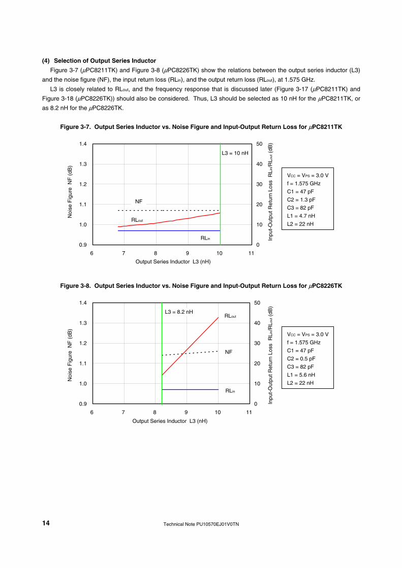
(4) Selection of Output Series Inductor
Figure 3-7 (µPC8211TK) and Figure 3-8 (µPC8226TK) show the relations between the output series inductor (L3)
and the noise figure (NF), the input return loss (RLin), and the output return loss (RLout), at 1.575 GHz.
L3 is closely related to RLout, and the frequency response that is discussed later (Figure 3-17 (µPC8211TK) and
Figure 3-18 (µPC8226TK)) should also be considered. Thus, L3 should be selected as 10 nH for the µPC8211TK, or
as 8.2 nH for the µPC8226TK.
Figure 3-7. Output Series Inductor vs. Noise Figure and Input-Output Return Loss for µPC8211TK
0.9
1.0
1.1
1.2
1.3
1.4
6 7 8 9 10 11
0
10
20
30
40
50
Figure 3-8. Output Series Inductor vs. Noise Figure and Input-Output Return Loss for µPC8226TK
0.9
1.0
1.1
1.2
1.3
1.4
6 7 8 9 10 11
0
10
20
30
40
50
VCC = VPS = 3.0 V
f = 1.575 GHz
C1 = 47 pF
C2 = 0.5 pF
C3 = 82 pF
L1 = 5.6 nH
L2 = 22 nH
VCC = VPS = 3.0 V
f = 1.575 GHz
C1 = 47 pF
C2 = 1.3 pF
C3 = 82 pF
L1 = 4.7 nH
L2 = 22 nH RLout
NF
RLin
L3 = 10 nH
Output Series Inductor L3 (nH)
Noi
se F
igur
e N
F (
dB)
Inpu
t-O
utpu
t Ret
urn
Loss
RLi
n/R
Lout (
dB)
RLout
NF
RLin
L3 = 8.2 nH
Output Series Inductor L3 (nH)
Noi
se F
igur
e N
F (
dB)
Inpu
t-O
utpu
t Ret
urn
Loss
RL i
n/R
Lout (
dB)

Technical Note PU10570EJ01V0TN 15
3. 1. 2 Frequency Characteristics of Noise Figure and Input-Output Return Loss
(1) Frequency Characteristics of Noise Figure
Figure 3-9 (µPC8211TK) and Figure 3-10 (µPC8226TK) show the frequency characteristics of the noise figure (NF)
and the NF associated gain (Ga). The NF associated gain is tuned to 1.575 GHz.
Figure 3-9. Noise Figure and NF Associated Gain vs. Frequency for µPC8211TK
0.9
1.0
1.1
1.2
1.3
1.4
1540 1550 1560 1570 1580 1590 1600 1610
10
12
14
16
18
20
Figure 3-10. Noise Figure and NF Associated Gain vs. Frequency for µPC8226TK
0.9
1.0
1.1
1.2
1.3
1.4
1540 1550 1560 1570 1580 1590 1600 1610
10
12
14
16
18
20
VCC = VPS = 3.0 V
C1 = 47 pF
C2 = 0.5 pF
C3 = 82 pF
L1 = 5.6 nH
L2 = 22 nH
L3 = 8.2 nH
VCC = VPS = 3.0 V
C1 = 47 pF
C2 = 1.3 pF
C3 = 82 pF
L1 = 4.7 nH
L2 = 22 nH
L3 = 10 nH
Frequency f (MHz)
Noi
se F
igur
e N
F (
dB)
NF
Ass
ocia
ted
Gai
n G
a (d
B)
Ga
NF
f = 1 575 MHz
Ga
NF
f = 1 575 MHz
Frequency f (MHz)
Noi
se F
igur
e N
F (
dB)
NF
Ass
ocia
ted
Gai
n G
a (d
B)

Technical Note PU10570EJ01V0TN 16
(2) Frequency Characteristics of Input Return Loss
Figure 3-11 (µPC8211TK) and Figure 3-12 (µPC8226TK) show the frequency characteristics of the input return
loss (RLin).
The amount of loss for RLin changes drastically as a result of selecting the input parallel capacitor (C2).
Also, as shown in Figure 3-1 (µPC8211TK) and Figure 3-2 (µPC8226TK), RLin and the noise figure (NF) stand in a
trade-off relation.
Figure 3-11. Input Return Loss vs. Frequency for µPC8211TK
1.575 2.475 0.475
20
10
0
VCC = VPS = 3.0 VC1 = 47 pFC3 = 82 pFL1 = 4.7 nHL2 = 22 nHL3 = 10 nH
C2 = 2.5 pF
C2 = 1.3 pF
C2 = 0.5 pF
1.575 2.475 0.475
20
10
0
VCC = VPS = 3.0 VC1 = 47 pFC3 = 82 pFL1 = 4.7 nHL2 = 22 nHL3 = 10 nH
C2 = 2.5 pF
C2 = 1.3 pF
C2 = 0.5 pF
Figure 3-12. Input Return Loss vs. Frequency for µPC8226TK
1.575 2.475 0.475
20
10
0
VCC = VPS = 3.0 VC1 = 47 pFC3 = 82 pFL1 = 5.6 nHL2 = 22 nHL3 = 8.2 nH
C2 = 2.2 pF
C2 = 0.3 pF
C2 = 0.5 pF
1.575 2.475 0.475
20
10
0
VCC = VPS = 3.0 VC1 = 47 pFC3 = 82 pFL1 = 5.6 nHL2 = 22 nHL3 = 8.2 nH
C2 = 2.2 pF
C2 = 0.3 pF
C2 = 0.5 pF
The input series inductor (L1) should be selected as the value where the resonance frequency matches the
approximate required frequency (1.575 GHz).
Although it would be ideal for the value of the resonance center frequency to precisely match the required
frequency of 1.575 GHz, due to limits imposed by the commercially available line-up of products (for example, the
next value after 4.7 nH being 5.6 nH), the best value out of those available should be selected. In this case, 4.7 nH
should be selected for the µPC8211TK, and 5.6 nH should be selected for the µPC8226TK.
Figure 3-13 shows the transition of the resonance center frequency in accordance with the value of L1, and Figure
3-14 shows the frequency characteristics of RLin when 4.7 nH is selected as the value of L1. Since the resonance
Inpu
t Ret
urn
Loss
RLi
n (d
B)
Frequency f (GHz)
Inpu
t Ret
urn
Loss
RLi
n (d
B)
Frequency f (GHz)

Technical Note PU10570EJ01V0TN 17
center frequency deviates a great deal from the target frequency (1.575 GHz) when the value of L1 is 4.7 nH,
adequate loss cannot be obtained for RLin even if C2 is changed.
Figure 3-13. Input Return Loss with Input Series Inductor vs. Frequency for µPC8226TK
L1 = 4.7 nH
L1 = 5.6 nH
1.575 2.4750.475
20
10
0
VCC = VPS = 3.0 VC1 = 47 pFC2 = 2.2 pFC3 = 82 pFL2 = 22 nHL3 = 8.2 nH
L1 = 4.7 nH
L1 = 5.6 nH
1.575 2.4750.475
20
10
0
VCC = VPS = 3.0 VC1 = 47 pFC2 = 2.2 pFC3 = 82 pFL2 = 22 nHL3 = 8.2 nH
Figure 3-14. Input Return Loss at L1 = 4.7 nH vs. Frequency for µPC8226TK
1.575 2.475 0.475
20
10
0
VCC = VPS = 3.0 VC1 = 47 pFC3 = 82 pFL1 = 4.7 nHL2 = 22 nHL3 = 8.2 nH
C2 = 0.3 pF
C2 = 2.2 pF
1.575 2.475 0.475
20
10
0
VCC = VPS = 3.0 VC1 = 47 pFC3 = 82 pFL1 = 4.7 nHL2 = 22 nHL3 = 8.2 nH
C2 = 0.3 pF
C2 = 2.2 pF
Inpu
t Ret
urn
Loss
RLi
n (d
B)
Frequency f (GHz)
Inpu
t Ret
urn
Loss
RLi
n (d
B)
Frequency f (GHz)

Technical Note PU10570EJ01V0TN 18
(3) Frequency Characteristics of Output Return Loss
Figure 3-15 (µPC8211TK) and Figure 3-16 (µPC8226TK) show the frequency characteristics of the output return
loss (RLout) in accordance with changes in the value of the output parallel inductor (L2), while Figure 3-17
(µPC8211TK) and Figure 3-18 (µPC8226TK) show the frequency characteristics of the output return loss (RLout) in
accordance with changes in the value of the output series inductor (L3).
The resonance center frequency is tuned to closely match the target frequency of 1.575 GHz through optimization
of the input series inductor (Figures 3-11 through 3-14). Thus, for L2 and L3, a value should be selected such that 10
dB or more can be obtained for RLout. Also, contribution to the noise figure (NF) should also be considered when
making a selection for L2 and L3 (Figures 3-5 through 3-8).
For L2, due to limits imposed by the commercially available line-up of inductors (for example, the next value after
18 nH being 22 nH), the best value out of those available should be selected. In this case, 22 nH should be selected
for both the µPC8211TK and the µPC8226TK. Similarly, for L3, due to limits imposed by the commercially available
line-up of inductors (for example, the next value after 8.2 nH being 10 nH), 10 nH should be selected for the
µPC8211TK, and 8.2 nH should be selected for the µPC8226TK.
Figure 3-15. Output Return Loss with Output Parallel Inductor vs. Frequency for µPC8211TK
L2 = 18 nH
L2 = 22 nH
L2 = 33 nH
1.575 2.475 0.475
40
20
0
VCC = VPS = 3.0 VC1 = 47 pFC2 = 1.3 pFC3 = 82 pFL1 = 4.7 nHL3 = 10 nH
L2 = 18 nH
L2 = 22 nH
L2 = 33 nH
1.575 2.475 0.475
40
20
0
VCC = VPS = 3.0 VC1 = 47 pFC2 = 1.3 pFC3 = 82 pFL1 = 4.7 nHL3 = 10 nH
Figure 3-16. Output Return Loss with Output Parallel Inductor vs. Frequency for µPC8226TK
L2 = 27 nH
L2 = 18 nH
L2 = 22 nH
1.575 2.475 0.475
40
20
0
VCC = VPS = 3.0 VC1 = 47 pFC2 = 0.5 pFC3 = 82 pFL1 = 5.6 nHL3 = 8.2 nH
L2 = 27 nH
L2 = 18 nH
L2 = 22 nH
1.575 2.475 0.475
40
20
0
VCC = VPS = 3.0 VC1 = 47 pFC2 = 0.5 pFC3 = 82 pFL1 = 5.6 nHL3 = 8.2 nH
Out
put R
etur
n Lo
ss R
Lout (
dB)
Frequency f (GHz)
Out
put R
etur
n Lo
ss R
Lout (
dB)
Frequency f (GHz)
Technical Note PU10570EJ01V0TN 19
Figure 3-17. Output Return Loss with Output Series Inductor vs. Frequency for µPC8211TK
1.575 2.475 0.475
50
25
0
VCC = VPS = 3.0 VC1 = 47 pFC2 = 1.3 pFC3 = 82 pFL1 = 4.7 nHL2 = 22 nH
L3 = 10 nH
L3 = 8.2 nH
L3 = 6.8 nH
1.575 2.475 0.475
50
25
0
VCC = VPS = 3.0 VC1 = 47 pFC2 = 1.3 pFC3 = 82 pFL1 = 4.7 nHL2 = 22 nH
L3 = 10 nH
L3 = 8.2 nH
L3 = 6.8 nH
Figure 3-18. Output Return Loss with Output Series Inductor vs. Frequency for µPC8226TK
L3 = 8.2 nH
L3 = 10 nH
1.575 2.475 0.475
50
25
0
VCC = VPS = 3.0 VC1 = 47 pFC2 = 0.5 pFC3 = 82 pFL1 = 5.6 nHL2 = 22 nH
L3 = 8.2 nH
L3 = 10 nH
1.575 2.475 0.475
50
25
0
VCC = VPS = 3.0 VC1 = 47 pFC2 = 0.5 pFC3 = 82 pFL1 = 5.6 nHL2 = 22 nH
Out
put R
etur
n Lo
ss R
Lout (
dB)
Frequency f (GHz)
Out
put R
etur
n Lo
ss R
Lout (
dB)
Frequency f (GHz)

Technical Note PU10570EJ01V0TN 20
3. 1. 3 Main Electrical Characteristics
Table 3-1 shows the main related electrical characteristics for the µPC8211TK and µPC8226TK.
The output series capacitor (C3) is a DC cut capacitor. When applied with a frequency in the vicinity of 1.575 GHz,
if a value of approximately 100 pF is selected, then the effect on the main high-frequency characteristics is negligible.
Also, the value for the parallel resistor (R1) is tuned to match the internal circuit constant of the MMIC.
Table 3-1. Main Electrical Characteristics for µPC8211TK and µPC8226TK
(TA = +25°C, VCC = 3.0 V, fin = 1 575 MHz, VPS = 3.0 V, unless otherwise specified)
Value Parameter Symbol Conditions
µPC8211TK µPC8226TK
Unit
Circuit Current ICC No Signal 3.7 3.1 mA
Noise Figure NF 0.90 1.07 1.69 1.12 1.14 1.73 dB
Power Gain GP Pin = −30 dBm 18.0 18.8 19.4 17.5 17.7 18.5 dB
Gain 1 dB Compression
Output Power
PO (1 dB) −3.8 −5.5 dBm
Output Power PO Pin = −10 dBm +2.5 +1.2 dBm
Input 3rd Order Distortion
Intercept Point
IIP3 −13.0 −12.0 dBm
Output 3rd Order Distortion
Intercept Point
OIP3 +6.0 +6.0 dBm
Input Return Loss RLin Pin = −30 dBm 5.1 7.0 15.0 6.4 7.0 15.3 dB
Output Return Loss RLout Pin = −10 dBm 16.7 17.4 18.5 15.0 14.1 13.7 dB
Isolation ISL Pin = −10 dBm 34.1 33.4 32.6 37.7 37.5 36.7 dB
C1 47 47 pF
C2 0.5 1.3 2.5 0.3 0.5 2.2 pF
C3 82 82 pF
L1 4.7 5.6 nH
L2 22 22 nH
L3 10 8.2 nH
Main Components
R1 750 750 Ω
3. 2 µPC8215TU (for use in PDAs)
The µPC8215TU has a gain best suited for use in PDAs (GP = 28 dB), and also has low noise characteristics (NF =
1.1 dB).
This section describes a usage example wherein the µPC8215TU is applied in a product implementing a 1.575
GHz GPS LNA.
An evaluation circuit for a 1.575 GHz GPS LNA that includes the µPC8215TU was shown previously in Figure 2-2.
3. 2. 1 Noise Figure and Input-Output Return Loss at 1.575 GHz
Figure 3-19 shows the characteristics for the input series capacitor (C1) and the noise figure (NF), and the input-
output return loss (RLin and RLout), at 1.575 GHz.
Figure 3-20 shows the characteristics for the input series inductor (L1) and the noise figure (NF), and the input-
output return loss (RLin and RLout), at 1.575 GHz.

Technical Note PU10570EJ01V0TN 21
C1 serves as a DC cut capacitor, but is also closely tied to the noise figure (NF).
In Figure 3-19, it can be seen that NF worsens when the value of C1 is approximately 40 pF or less, but when the
value of C1 is approximately 40 pF or more, NF, RLin and RLout maintain constant values. Thus, 47 pF should be
selected as the value of C1.
The output series capacitor (C3) is also a DC cut capacitor. When applied with a frequency in the vicinity of 1.575
GHz, if a value of approximately 100 pF is selected, then the effect on the main electrical characteristics is negligible.
The input series inductor (L1) is closely tied to NF. As shown in Figure 3-20, 2.7 nH should be selected in order to
optimize NF.
Table 2-1, shown previously, describes the main electrical characteristics of the µPC8215TU.
Figure 3-19. Input Series Capacitor vs. Noise Figure and Input-Output Return Loss for µPC8215TU
0.9
1.0
1.1
1.2
1.3
1.4
0 10 20 30 40 50 60 70 80 90 100 110
0
5
10
15
20
25
C1 = 47 pF
RLout
NF
RLin VCC = 3.0 V
f = 1.575 GHz
C3 = 100 pF
L1 = 2.7 nH
Input Series Capacitor C1 (pF)
Noi
se F
igur
e N
F (
dB)
Inpu
t-O
utpu
t Ret
urn
Loss
R
Lin/
RLo
ut (
dB)
Figure 3-20. Input Series Inductor vs. Noise Figure and Input-Output Return Loss for µPC8215TU
0.9
1.0
1.1
1.2
1.3
1.4
1.5 2 2.5 3 3.5 4 4.5
0
5
10
15
20
25
L1 = 2.7 nH
RLout
NF
RLin VCC = 3.0 V
f = 1.575 GHz
C1 = 47 pF
C3 = 100 pF
Input Series Inductor L1 (nH)
Noi
se F
igur
e N
F (
dB)
Inpu
t-O
utpu
t Ret
urn
Loss
R
Lin/
RLo
ut (
dB)

Technical Note PU10570EJ01V0TN 22
3. 2. 2 Frequency Characteristics of Noise Figure
Figure 3-21 shows the frequency characteristics of the noise figure (NF) and the NF associated gain (Ga).
Figure 3-21. Noise Figure and NF Associated Gain vs. Frequency for µPC8215TU
0.9
1.0
1.1
1.2
1.3
1.4
1540 1550 1560 1570 1580 1590 1600 1610
10
15
20
25
30
35
f = 1.575 MHz
NF
VCC = 3.0 V
C1 = 47 pF
C3 = 100 pF
L1 = 2.7 nH
Frequency f (MHz)
Noi
se F
igur
e N
F (
dB)
NF
Ass
ocia
ted
Gai
n G
a (d
B)
Ga

Technical Note PU10570EJ01V0TN 23
3. 3 Measurement Circuit Configuration
3. 3. 1 NF Measurement Circuit Configuration
Figure 3-22 shows the NF measurement circuit configuration.
Figure 3-22. NF Measurement Circuit
EC-µPC8211TKor
EC-µPC8226TKor
EC-µPC8215TU
HP346C (APC3.5connector type)
HP8970B
DC Voltage Current Source: Advantest TR6143
Noise SourceNF
MeasurementCircuit
RF-IN RF-OUTEC-µPC8211TKor
EC-µPC8226TKor
EC-µPC8215TU
HP346C (APC3.5connector type)
HP8970B
DC Voltage Current Source: Advantest TR6143
Noise SourceNF
MeasurementCircuit
RF-IN RF-OUT
3. 3. 2 S-Parameter Measurement Circuit Configuration
Figure 3-23 shows the S-parameter measurement circuit configuration.
Figure 3-23. S-Parameter Measurement Circuit
HP8719D
NetworkAnalyzer
RF-IN RF-OUTEC-µPC8211TKor
EC-µPC8226TKor
EC-µPC8215TUDC Voltage Current Source: Advantest TR6143
HP8719D
NetworkAnalyzer
RF-IN RF-OUTEC-µPC8211TKor
EC-µPC8226TKor
EC-µPC8215TUDC Voltage Current Source: Advantest TR6143

Technical Note PU10570EJ01V0TN 24
4. BOARD ASSEMBLY & STANDARD ELECTRICAL CHARACTERISTICS
This section describes boards and components used to build evaluation boards using the µPC8211TK,
µPC8226TK, and the µPC8215TU for the LNAs of GPS systems at 1.575 GHz. Information on component
implementation examples is also provided. The standard electrical characteristics for each evaluation board are also
given.
4. 1 Product Information
4. 1. 1 Ordering Information
Table 4-1. Ordering Information
Part Number Order Number Package Marking Supplying Form
µPC8211TK-E2 µPC8211TK-E2-A 6G
µPC8226TK-E2 µPC8226TK-E2-A
6-pin lead-less minimold
(1511 PKG) (Pb-Free) Note
6H
• Embossed tape, 8 mm wide
• Pins 1, 6 face the perforation side of the tape
• Qty 5 kpcs/reel
µPC8215TU-E2 µPC8215TU-E2-A 8-pin lead-less minimold
(Pb-Free) Note
8215 • Embossed tape, 8 mm wide
• Pins 5, 6, 7, 8 indicate pull-out direction of tape
• Qty 5 kpcs/reel
Note With regards to terminal solder (the solder contains lead) plated products (conventionally plated), contact
your nearby sales office.
Technical Note PU10570EJ01V0TN 25
4. 1. 2 Pin Connections
The µPC8211TK and the µPC8226TK are implemented in a 6-pin lead-less minimold package, and the pin
connections are the same for both. However, the markings differ for the two. The µPC8211TK has a marking that
reads “6G”, while the µPC8226TK has a marking that reads “6H”.
The µPC8215TU is implemented in an 8-pin lead-less minimold package, and has a marking that reads “8215”.
Figure 4-1. µPC8211TK
Pin No. Pin Name
1 INPUT
2 GND
3 PS
4 OUTPUT
5 GND
6
5
4
(Bottom View)
1
2
3
1
2
3
(Top View)
6
5
4
6G
6 VCC
Figure 4-2. µPC8226TK
Pin No. Pin Name
1 INPUT
2 GND
3 PS
4 OUTPUT
5 GND
6
5
4
(Bottom View)
1
2
3
1
2
3
(Top View)
6
5
46H
6 VCC
Figure 4-3. µPC8215TU
Pin No. Pin Name
1 GND
2 INPUT
3 GND
4 GND
5 VCC
6 GND
7 OUTPUT
1
2
3
4
8
7
6
5
1
2
3
4
8
7
6
5
8215
(Bottom View)(Top View)
8 GND

Technical Note PU10570EJ01V0TN 26
4. 1. 3 Internal Block Diagram
Figure 4-4. Internal Block Diagram
(1) µPC8211TK and µPC8226TK (2) µPC8215TU
Includes a power-save function. Configured as a 2-stage amplifier.
5
6
7
8
4
3
2
1GND
INPUT
GND
GND
GND
OUTPUT
GND
VCC
INPUT 1
Bias
2
3
GND
PS
VCC6
5
4
GND
OUTPUT

Technical Note PU10570EJ01V0TN 27
4. 2 Evaluation Board for a 1.575 GHz GPS LNA with µPC8211TK
4. 2. 1 Evaluation Board Pattern Layout
Photo 4-1. Board Pattern Layout for µPC8211TK
Magnified

Technical Note PU10570EJ01V0TN 28
Figure 4-5. Pattern Layout
SIZE 16.36 mm × 21.46 mm
MATERIAL FR4 (ELC4756UV/Sumitomo), double side copper-clad,
t = 0.2 mm (total: t = 1.0 mm), εr = 4.6, Au flash plated on pattern
PC TERMINAL A2-2PA-2.54DSA (HIROSE)
RF CONNECTOR WK72475 (WAKA)
THROUGH HOLES
Table 4-2. Components of Test Circuit for Measuring Electrical Characteristics
Symbol Form Rating Part Number Maker
C1 Chip Capacitor 47 pF GRM1552C1H470JZ01 Murata
C2 Chip Capacitor 1.3 pF GRM1554C1H1R3CZ01 Murata
C3 Chip Capacitor 82 pF GRM1552C1H820JZ01 Murata
C4, C5 Chip Capacitor 1 000 pF GRM1552C1H102JA01 Murata
R1 Chip Resistor 750 Ω RR-0510P-751D Susumu
L1 Chip Inductor 4.7 nH AML1005H4N7ST FDK
L2 Chip Inductor 22 nH AML1005H22NST FDK
L3 Chip Inductor 10 nH AML1005H10NST FDK

Technical Note PU10570EJ01V0TN 29
4. 2. 2 Standard Electrical Characteristics
Main Standard Electrical Characteristics for Reference
(TA = +25°C, VCC = 3.0 V, VPS = 3.0 V, fin = 1 575 MHz, unless otherwise specified)
ICC: 3.7 mA IIP3: −13 dBm
NF: 1.07 dB RLin: 7.0 dB
GP: 18.8 dB RLout: 17.4 dB
PO (1 dB): −3.8 dBm ISL: 33.4 dB
PO: +2.5 dBm @Pin = −10 dBm
Figure 4-6. Evaluation Circuit
61
2
3
5
4VPS
IN
OUT
VCC
C1
C2
C4
L1C5
R1 L2
L3 C382 pF
4.7 nH
1.3 pF
47 pF
10 nH1 000 pF
1 000 pF
750 Ω 22 nH
High: ONLow: OFF (Power-Save)

Technical Note PU10570EJ01V0TN 30
Figure 4-7. Gain and Isolation
Pow
er G
ain
GP (
dB)
Isol
atio
n IS
L (d
B)
Frequency f (GHz)

Technical Note PU10570EJ01V0TN 31
Figure 4-8. Input and Output Return Loss
Inpu
t Ret
urn
Loss
RLi
n (d
B)
Out
put R
etur
n Lo
ss R
Lout (
dB)
Frequency f (GHz)

Technical Note PU10570EJ01V0TN 32
Figure 4-9. S-Parameter
S11
Start 0.1 GHz
Stop 3.0 GHz
(measured at
connector on
application
board)
S22
Start 0.1 GHz
Stop 3.0 GHz
(measured at
connector on
application
board)

Technical Note PU10570EJ01V0TN 33
Figure 4-10. Input 3rd Order Distortion Intercept Point
2tone Pout vs. P in (EC-µ PC8211TK_0.2FR4)
-80
-70
-60
-50
-40
-30
-20
-10
0
10
-45 -40 -35 -30 -25 -20 -15 -10 -5 0
Pin /tone (dBm)
Pou
t /to
ne (
dBm
)
IIP3 = −13 dBm
Pout _RF
Pout _IM3
HP8562AfRF1 = 1 575.5 MHzfRF2 = 1 575.6 MHzfIM3L = 1 575.4 MHzfIM3H = 1 575.7 MHzSpan 1 MHzATT autoRBW 30 KHzVBW 10 KHzSWP 50 mSRef level 0 dBm
OUTPUT POWER vs. INPUT POWERO
utpu
t Pow
er/T
one
Pou
t (dB
m)
Input Power/Tone Pin (dBm)
Figure 4-11. Gain 1 dB Compression Output Power
Pout vs. Pin (EC-µ PC8211TK_0.2FR4)
-25
-20
-15
-10
-5
0
5
10
-45 -40 -35 -30 -25 -20 -15 -10 -5 0 5
Pin (dBm)
Pou
t (dB
m)
PO = +2.5 dBm @Pin = −10 dBm
PO (1 dB) = −3.8 dBm
VCC = 3.0 VICC = 3.6 mAFrequency 1 575 MHzHP483A POWER METERHP8665A GENERATOR
Pout
PO (1 dB)
OUTPUT POWER vs. INPUT POWER
Out
put P
ower
P
out (
dBm
)
Input Power Pin (dBm)

Technical Note PU10570EJ01V0TN 34
4. 3 Evaluation Board for a 1.575 GHz GPS LNA with µPC8226TK
4. 3. 1 Evaluation Board Pattern Layout
Photo 4-2. Board Pattern Layout for µPC8226TK
Magnified

Technical Note PU10570EJ01V0TN 35
Figure 4-12. Pattern Layout
SIZE 16.36 mm × 21.46 mm
MATERIAL FR4 (ELC4756UV/Sumitomo), double side copper-clad,
t = 0.2 mm (total: t = 1.0 mm), εr = 4.6, Au flash plated on pattern
PC TERMINAL A2-2PA-2.54DSA (HIROSE)
RF CONNECTOR WK72475 (WAKA)
THROUGH HOLES
Table 4-3. Components of Test Circuit for Measuring Electrical Characteristics
Symbol Form Rating Part Number Maker
C1 Chip Capacitor 47 pF GRM1552C1H470JZ01 Murata
C2 Chip Capacitor 0.5 pF GRM1554C1H0R5CZ01 Murata
C3 Chip Capacitor 82 pF GRM1552C1H820JZ01 Murata
C4, C5 Chip Capacitor 1 000 pF GRM1552C1H102JA01 Murata
R1 Chip Resistor 750 Ω RR-0510P-751D Susumu
L1 Chip Inductor 5.6 nH AML1005H5N6ST FDK
L2 Chip Inductor 22 nH AML1005H22NST FDK
L3 Chip Inductor 8.2 nH AML1005H8N2ST FDK

Technical Note PU10570EJ01V0TN 36
4. 3. 2 Standard Electrical Characteristics
Main Standard Electrical Characteristics for Reference
(TA = +25°C, VCC = 3.0 V, VPS = 3.0 V, fin = 1 575 MHz, unless otherwise specified)
ICC: 3.1 mA IIP3: −12 dBm
NF: 1.14 dB RLin: 7.0 dB
GP: 17.7 dB RLout: 14.1 dB
PO (1 dB): −5.5 dBm ISL: 37.5 dB
PO: +1.2 dBm @Pin = −10 dBm
Figure 4-13. Evaluation Circuit
61
2
3
5
4VPS
IN
OUT
VCC
C1
C2
C4
L1C5
R1 L2
L3 C382 pF
5.6 nH
0.5 pF
47 pF
8.2 nH1 000 pF
1 000 pF
750 Ω 22 nH
High: ONLow: OFF (Power-Save)

Technical Note PU10570EJ01V0TN 37
Figure 4-14. Gain and Isolation
Pow
er G
ain
GP (
dB)
Isol
atio
n IS
L (d
B)
Frequency f (GHz)

Technical Note PU10570EJ01V0TN 38
Figure 4-15. Input and Output Return Loss
Inpu
t Ret
urn
Loss
RLi
n (d
B)
Out
put R
etur
n Lo
ss R
Lout (
dB)
Frequency f (GHz)

Technical Note PU10570EJ01V0TN 39
Figure 4-16. S-Parameter
S11
Start 0.1 GHz
Stop 3.0 GHz
(measured at
connector on
application
board)
S22
Start 0.1 GHz
Stop 3.0 GHz
(measured at
connector on
application
board)

Technical Note PU10570EJ01V0TN 40
Figure 4-17. Input 3rd Order Distortion Intercept Point
2tone Pout vs. Pin (EC-µ PC8226TK_0.2FR4)
-80
-70
-60
-50
-40
-30
-20
-10
0
10
-50 -40 -30 -20 -10 0
Pin /tone (dBm)
Pou
t /to
ne (
dBm
)
IIP3 = −12 dBm
Pout _RF
Pout _IM3
HP8562AfRF1 = 1 575.5 MHzfRF2 = 1 575.6 MHzfIM3L = 1 575.4 MHzfIM3H = 1 575.7 MHzSpan 1 MHzATT autoRBW 30 KHzVBW 10 KHzSWP 50 mSRef level 0 dBm
OUTPUT POWER vs. INPUT POWERO
utpu
t Pow
er/T
one
Pou
t (dB
m)
Input Power/Tone Pin (dBm)
Figure 4-18. Gain 1 dB Compression Output Power
-25
-20
-15
-10
-5
0
5
10
-45 -40 -35 -30 -25 -20 -15 -10 -5 0 5
PO = +1.2 dBm@Pin = −10 dBm
PO (1 dB) = −5.5 dBm
VCC = 3.0 VICC = 3.1 mAFrequency 1 575 MHzHP483A POWER METERHP8665A GENERATOR
PO (1 dB)
Pout
OUTPUT POWER vs. INPUT POWER
Out
put P
ower
P
out (
dBm
)
Input Power Pin (dBm)

Technical Note PU10570EJ01V0TN 41
4. 4 Evaluation Board for a 1.575 GHz GPS LNA with µPC8215TU
4. 4. 1 Evaluation Board Pattern Layout
Photo 4-3. Board Pattern Layout for µPC8215TU
Magnified

Technical Note PU10570EJ01V0TN 42
Figure 4-19. Pattern Layout
SIZE 18.7 mm × 28 mm
MATERIAL FR4 (ELC4756UV/Sumitomo), double side copper-clad,
t = 0.4 mm, εr = 4.6, Au flash plated on pattern
PC TERMINAL A2-2PA-2.54DSA (HIROSE)
RF CONNECTOR WK72475 (WAKA)
THROUGH HOLES
Table 4-4. Components of Test Circuit for Measuring Electrical Characteristics
Symbol Form Rating Part Number Maker
C1 Chip Capacitor 47 pF GRM1552C1H470JZ01 Murata
C3 Chip Capacitor 100 pF GRM1552C1H101JZ01 Murata
C5 Chip Capacitor 1 000 pF GRM1552C1H102JA01 Murata
L1 Chip Inductor 2.7 nH AML1005H2N7ST FDK

Technical Note PU10570EJ01V0TN 43
4. 4. 2 Standard Electrical Characteristics
Main Standard Electrical Characteristics for Reference
(TA = +25°C, VCC = 3.0 V, fin = 1 575 MHz, unless otherwise specified)
ICC: 12.0 mA OIP3: +13 dBm
NF: 1.08 dB RLin: 6.8 dB
GP: 28.5 dB RLout: 17.2 dB
PO (1 dB): +7.6 dBm ISL: 45.6 dB
Figure 4-20. Evaluation Circuit
VCC
INPUT
5
6
7
8
4
2
1
3
OUTPUT
C1 L1
C51 000 pF
C347 pF 2.7 nH 100 pF

Technical Note PU10570EJ01V0TN 44
Figure 4-21. Gain and Isolation
Pow
er G
ain
GP (
dB)
Isol
atio
n IS
L (d
B)
Frequency f (GHz)

Technical Note PU10570EJ01V0TN 45
Figure 4-22. Input and Output Return Loss
Inpu
t Ret
urn
Loss
RLi
n (d
B)
Out
put R
etur
n Lo
ss R
Lout (
dB)
Frequency f (GHz)

Technical Note PU10570EJ01V0TN 46
Figure 4-23. S-Parameter
S11
Start 0.1 GHz
Stop 3.0 GHz
(measured at
connector on
application
board)
S22
Start 0.1 GHz
Stop 3.0 GHz
(measured at
connector on
application
board)

Technical Note PU10570EJ01V0TN 47
Figure 4-24. Output 3rd Order Distortion Intercept Point
2tone Pout vs. P in (EC-µ PC8215TU_0.2FR4)
-60
-50
-40
-30
-20
-10
0
10
20
-50 -40 -30 -20 -10 0
Pin /tone (dBm)
Pou
t /to
ne (
dBm
)
OIP3 = 13 dBm
Pout_RF
Pout _IM3
HP8562AfRF1 = 1 575.5 MHzfRF2 = 1 575.6 MHzfIM3L = 1 575.4 MHzfIM3H = 1 575.7 MHzSpan 1 MHzATT autoRBW 10 KHzVBW 10 KHzSWP 50 mSRef level 0 dBm
OUTPUT POWER vs. INPUT POWERO
utpu
t Pow
er/T
one
Pou
t (dB
m)
Input Power/Tone Pin (dBm)
OIP3 = +13 dBm
Figure 4-25. Gain 1 dB Compression Output Power
Pout vs. Pin (EC-µ PC8215TU_0.2FR4)
-20
-15
-10
-5
0
5
10
-45 -40 -35 -30 -25 -20 -15 -10 -5 0Pin (dBm)
Pou
t (dB
m)
PO (1 dB) = +7.6 dBm
VCC = 3.0 VICC = 12.0 mAFrequency 1 575 MHzHP483A POWER METERHP8665A GENERATOR
Pout
PO (1 dB)
OUTPUT POWER vs. INPUT POWER
Out
put P
ower
P
out (
dBm
)
Input Power Pin (dBm)

NEC Compound Semiconductor Devices Hong Kong Limited E-mail: [email protected] (sales, technical and general) Hong Kong Head Office Taipei Branch Office Korea Branch Office
TEL: +852-3107-7303TEL: +886-2-8712-0478TEL: +82-2-558-2120
FAX: +852-3107-7309 FAX: +886-2-2545-3859FAX: +82-2-558-5209
NEC Electronics (Europe) GmbH http://www.ee.nec.de/ TEL: +49-211-6503-0 FAX: +49-211-6503-1327
California Eastern Laboratories, Inc. http://www.cel.com/ TEL: +1-408-988-3500 FAX: +1-408-988-0279 0504
NEC Compound Semiconductor Devices, Ltd. http://www.ncsd.necel.com/ E-mail: [email protected] (sales and general) [email protected] (technical) Sales Division TEL: +81-44-435-1573 FAX: +81-44-435-1579
For further information, please contact


![DC Lines and Electronic Devices · (GHz) to improve the accuracy of positional location[1,2,3,5,6,7,8,9,10, 11,12]; this is called differential GPS (DGPS). Some GPS systems also make](https://img.dokumen.tips/doc/110x75/5f68dbc5ac2a9243fe77fefc/dc-lines-and-electronic-devices-ghz-to-improve-the-accuracy-of-positional-location1235678910.jpg)