Embed Size (px)
Citation preview

AppendixSolution for Current Reference ShiftingIntegration
The following solution solves two issues of the implemented ADC described inChap. 5: integration of the currents for reference shifting and reduction (andcontrol) of the reference shifting period to allow linear settling before the end ofthe amplification phase [127]. As already described in Sect. 3.2, a current-modereference shifting technique is employed to substitute the voltage referencecircuits. The objective is to emulate the effect of a reference voltage (VREF), whichcan be achieved using a capacitor, a current, and a certain amount of time, i.e.,DV ¼ IDt=C. In an SC-MDAC circuit, two of the three mentioned quantities arereadily available: the capacitor is the one found in the opamp’s feedback loop, themaximum time available is the amplification phase, and only a current sourceneeds to be added to the circuit (substituting the reference voltage). To determinethe correct amount of current for reference shifting, a global reference shiftingcontroller, composed of a replica of a pipeline stage and a discrete SC-integrator,is used (Fig. 1.1). These two circuits operate together to generate the biasingvoltages for the cascode current mirrors and sources of all the ADC’s stages. Notethat, the VREF of Fig 1.1 does not need to be buffered.
A.1 Replica Stage
As the name indicates the replica stage is an exact copy of a pipelined stage. Anydeviations or changes to the circuit’s nominal operation will be reflected in thisreplica stage, and therefore, corrected. The replica circuit helps minimizing issuescaused by charge injection of the MDAC’s current control switches, duty-cycledeviation between the main phases, and undesired parasitic effects (opamp’s input,etc.). Scaling of the replica stage is possible, with respective degradation ofreference shifting accuracy. Given that the ADC’s performance depends on thematching between the replica and the ADC’s stages, caution must be taken duringtransistor sizing to avoid large mismatches.
M. Figueiredo et al., Reference-Free CMOS Pipeline Analog-to-Digital Converters,Analog Circuits and Signal Processing, DOI: 10.1007/978-1-4614-3467-2,� Springer Science+Business Media New York 2013
167
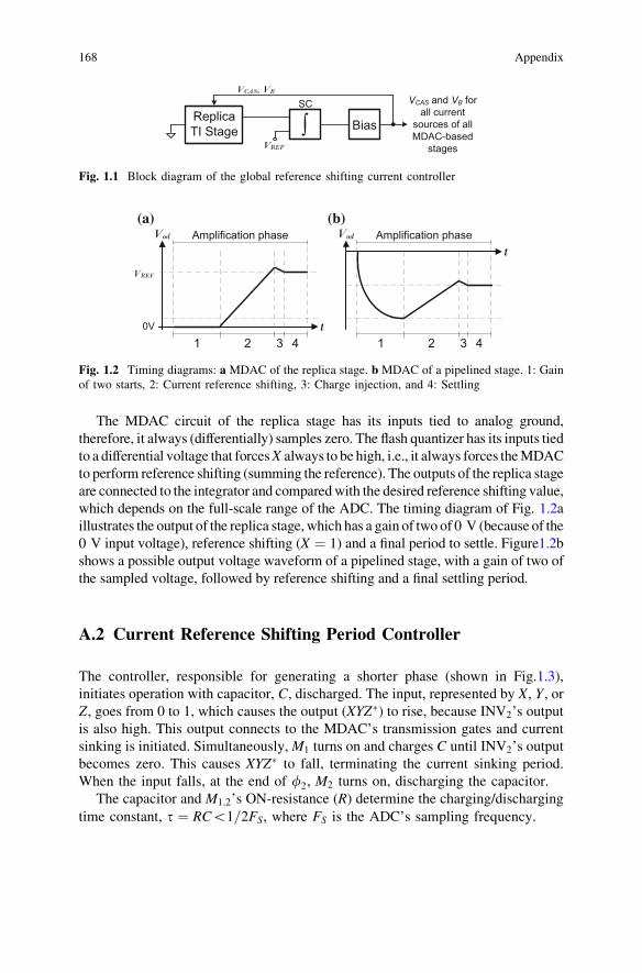
The MDAC circuit of the replica stage has its inputs tied to analog ground,therefore, it always (differentially) samples zero. The flash quantizer has its inputs tiedto a differential voltage that forces X always to be high, i.e., it always forces the MDACto perform reference shifting (summing the reference). The outputs of the replica stageare connected to the integrator and compared with the desired reference shifting value,which depends on the full-scale range of the ADC. The timing diagram of Fig. 1.2aillustrates the output of the replica stage, which has a gain of two of 0 V (because of the0 V input voltage), reference shifting (X ¼ 1) and a final period to settle. Figure1.2bshows a possible output voltage waveform of a pipelined stage, with a gain of two ofthe sampled voltage, followed by reference shifting and a final settling period.
A.2 Current Reference Shifting Period Controller
The controller, responsible for generating a shorter phase (shown in Fig.1.3),initiates operation with capacitor, C, discharged. The input, represented by X, Y , orZ, goes from 0 to 1, which causes the output (XYZ�) to rise, because INV2’s outputis also high. This output connects to the MDAC’s transmission gates and currentsinking is initiated. Simultaneously, M1 turns on and charges C until INV2’s outputbecomes zero. This causes XYZ� to fall, terminating the current sinking period.When the input falls, at the end of /2, M2 turns on, discharging the capacitor.
The capacitor and M1;2’s ON-resistance (R) determine the charging/dischargingtime constant, s ¼ RC\1=2FS, where FS is the ADC’s sampling frequency.
Fig. 1.1 Block diagram of the global reference shifting current controller
(a) (b)
Fig. 1.2 Timing diagrams: a MDAC of the replica stage. b MDAC of a pipelined stage. 1: Gainof two starts, 2: Current reference shifting, 3: Charge injection, and 4: Settling
168 Appendix

A.3 Discrete SC-Integrator
The SC-integrator, as shown in Fig.1.4, is based on the conventional parasitic-insensitive architecture. The circuit diagram illustrates an integrator for a time-interleaved ADC with two channels. For single channel ADCs, one of the channelsof the integrator is removed. The outputs of the replica stage are connected to theintegrator and are compared (differentially) with the desired reference shiftingvoltage. The output of the integrator drives a current mirror of the biasing circuit togenerate two biasing voltages, VCAS and VB. These voltages drive the currentsources of the replica stage (and the current sources of all stages of the ADC) in anegative feedback loop. This analog calibration scheme allows to continuouslyadjust the biasing voltages until the desired reference shifting is achieved, takinginto account all the nonidealities of a pipeline stage.
Fig. 1.3 Circuit diagram of the current reference shifting period controller
Fig. 1.4 Integrator circuit for time-interleaved stages. For single channel ADCs, one of thechannels of the integrator may be discarded
Appendix 169

References
1. Abo AM (1999) Design for reliability of low-voltage, switched-capacitor circuits. PhDthesis, University of California at Berkeley
2. Achigui H, Fayomi C, Sawan M (2003) A DTMOS-based 1 V opamp. In: Proceedings IEEEInternational Conference Electronics, Circuits, Systems (ICECS), pp 252–255
3. AD (2011) Analog Devices AD9484. http://www.analog.com/en/analog-to-digital-converters/ad-converters/ad9484/products/product.html
4. Ahmed I, Johns D (2007) An 11-bit 45MS/s pipelined ADC with rapid calibration of DACerrors in a multi-bit pipeline stage. In: Proceedings of European Solid-State CircuitsConference (ESSCIRC), pp 147–150
5. Ahuja B (1983) An improved frequency compensation technique for CMOS operationalamplifiers. IEEE J Solid-State Circuits 18(6):629-633
6. Alpman E, Lakdawala H, Carley L, Soumyanath K (2009) A 1.1V 50mW 2.5GS/s 7b time-interleaved C-2C SAR ADC in 45nm LP digital CMOS. In: IEEE International Solid-StateCircuits Conference (ISSCC) Digest Technical Papers
7. Assaad R, Silva-Martinez J (2009) The recycling folded cascode A general enhancement ofthe folded cascode amplifier. IEEE J Solid-State Circuits 44(9):2535–2542
8. Bajdechi O, Huijsing J (2002) A 1.8-V DR modulator interface for an electret microphonewith on-chip reference. IEEE J Solid-State Circuits 37(3):279–285
9. Baker RJ (2010) CMOS : circuit design, layout, and simulation, 3rd edn. Wiley-IEEE Press,Hoboken
10. Bazes M (1991) Two novel fully complementary self-biased CMOS differential amplifiers.IEEE J Solid-State Circuits 26(2):165–168
11. Black WC, Hodges DA (1980) Time interleaved converter arrays. IEEE J Solid-StateCircuits 15(6):1022–1029
12. Borghetti F, Nielsen JH, Ferragina V, Malcovati P, Andreani P, Baschirotto A (2006) Aprogrammable 10b up-to-6MS/s SAR-ADC featuring constant-FoM with on-chip referencevoltage buffers. In: Proceedings of European Solid-State Circuits Conference (ESSCIRC),pp 500–503
13. Boulemnakher M, Andre E, Roux J, Paillardet F (2008) A 1.2V 4.5mW 10b 100MS/spipeline ADC in a 65nm CMOS. In: IEEE International Solid-State Circuits Conference(ISSCC) Digest Technical Papers, pp 250–611
14. Brewer R, Gorbold J, Hurrell P, Lyden C, Maurino R, Vickery M (2005) A 100dB SNR2.5MS/s output data rate DR ADC. In: IEEE International Solid-State Circuits Conference(ISSCC) Digest Technical Papers, vol 1, pp 172–591
M. Figueiredo et al., Reference-Free CMOS Pipeline Analog-to-Digital Converters,Analog Circuits and Signal Processing, DOI: 10.1007/978-1-4614-3467-2,� Springer Science+Business Media New York 2013
171
15. Brooks L, Lee HS (2007) A zero-crossing-based 8-bit 200 MS/s pipelined ADC. IEEE JSolid-State Circuits 42(12):2677–2687
16. Brooks T, Robertson D, Kelly D, Del Muro A, Harston S (1997) A cascaded sigma-deltapipeline A/D converter with 1.25 MHz signal bandwidth and 89 dB SNR. IEEE J Solid-State Circuits 32(12):1896–1906
17. Bult K (2009) Embedded analog-to-digital converters. In: Proceedings of European Solid-State Circuits Conference (ESSCIRC), pp 52–64
18. Callewaert L, Sansen W (1990) Class AB CMOS amplifiers with high efficiency. IEEE JSolid-State Circuits 25(3):684–691
19. Cao Z, Song T, Yan S (2007) A 14 mW 2.5 MS/s 14 bit RD modulator using split-pathpseudo-differential amplifiers. IEEE J Solid-State Circuits 42(10):2169–2179
20. Cao Z, Yan S, Li Y (2009) A 32 mW 1.25 GS/s 6b 2b/Step SAR ADC in 0.13lm CMOS.IEEE J Solid-State Circuits 44(3):862–873
21. Chandrashekar K, Bakkaloglu B (2011) A 10 b 50 MS/s opamp-sharing pipeline A/D withcurrent-reuse OTAs. IEEE Trans VLSI Syst 19(9):1610–1616
22. Chang TH, Dung LR (2008) Fourth-Order cascaded RD modulator using tri-levelquantization and bandpass noise shaping for broadband telecommunication applications.IEEE Trans Circuits Syst I, Reg Papers 55(6):1722–1732
23. Chang TH, Dung LR (2008) Fourth-order cascaded RD modulator using tri-levelquantization and bandpass noise shaping for broadband telecommunication applications.IEEE Trans Circuits Syst I, Reg Papers 55(6):1722–1732
24. Chang TH, Dung LR, Guo JY, Yang KJ (2007) A 2.5-V 14-bit, 180-mW cascaded RD ADCfor ADSL2+ application. IEEE J Solid-State Circuits 42(11):2357–2368
25. Chen HS, Song BS, Bacrania K (2001) A 14-b 20-Msamples/s CMOS pipelined ADC. IEEEJ Solid-State Circuits 36(6):997–1001
26. Chen HW, Chen IC, Tseng HC, Chen HS (2009) A 1-GS/s 6-bit two-channel two-step ADCin 0.13-lm CMOS. IEEE J Solid-State Circuits 44(11):3051–3059
27. Chew K, Yeo K, Chu SF (2004) Effect of technology scaling on the 1/f noise of deepsubmicron PMOS transistors. Elsevier Solid-State Electronics 48(7):1101–1109
28. Chilakapati U, Fiez T (1998) Settling time design considerations for SC integrators. In:Proceedings of IEEE International Symposium Circuits Systems (ISCAS), vol 1, pp 492–495
29. Chiu Y (2000) Inherently linear capacitor error-averaging techniques for pipelined A/Dconversion. IEEE Trans Circuits Syst II 47(3):229–232
30. Chiu Y, Gray PR, Nikolic B (2004) A 14-b 12-MS/s CMOS pipeline ADC with over 100-dBsfdr. IEEE J Solid-State Circuits 39(12):2139–2151
31. Cho YJ, Lee SH (2005) An 11b 70-MHz 1.2-mm2 49-mW 0.18-lm CMOS ADC with on-chip current/voltage references. IEEE Trans Circuits Syst I, Reg Papers 52(10):1989–1995
32. Cho YJ, Bae HH, Lee MJ, Kim MJ, Lee SH, Kim YL (2004) An 8b 220 MS/s 0.25 lmCMOS pipeline ADC with on-chip RC-filter based voltage references. In: Proceedings ofIEEE Asia-Pacific Conference Advanced Systems Integrated Circuits, pp 90–93
33. Cho YK, Jeon YD, Nam JW, Kwon JK (2010) A 9-bit 80 MS/s successive approximationregister analog-to-digital converter with a capacitor reduction technique. IEEE TransCircuits Syst II, Exp Briefs 57(7):502–506
34. Choi HC, Kim YJ, Yoo SW, Hwang SY, Lee SH (2008) A programmable 0.8-V 10-bit 60-MS/s 192-mW 013-lm CMOS ADC operating down to 0 5 V. IEEE Trans Circuits Syst II,Exp Briefs 55(4):319–323
35. Choksi O, Carley L (2003) Analysis of switched-capacitor common-mode feedback circuit.IEEE Trans Circuits Syst II 50(12):906–917
36. Christen T, Huang Q (2010) A 0.13 lm CMOS 0.1-20MHz bandwidth 86-70dB DR multi-mode DT DR ADC for imt-advanced. In: Proceedings of European Solid-State CircuitsConference (ESSCIRC), pp 414–417
37. Conroy CSG, Cline DW, Gray PR (1993) An 8-b 85-MS/s parallel pipeline A/D converter in1-lm CMOS. IEEE J Solid-State Circuits 28(4):447–454
172 References
38. Custódio J, Oliveira L, Goes J, Oliveira J, Bruun E, Andreani P (2010) A small-area self-biased wideband CMOS balun LNA with noise cancelling and gain enhancement. In:NORCHIP, pp 1–4
39. Daihong F, Dyer KC, Lewis SH, Hurst PJ (1998) A digital background calibration technique fortime-interleaved analog-to-digital converters. IEEE J Solid-State Circuits 33(12):1904–1911
40. del Rio R, de la Rosa J, Perez-Verdu B, Delgado-Restituto M, Dominguez-Castro R,Medeiro F, Rodriguez-Vazquez A (2004) Highly linear 2.5-V CMOS RD modulator forADSL+. IEEE Trans Circuits Syst I, Reg Papers 51(1):47–62
41. Dessouky M, Kaiser A (1999) Input switch configuration suitable for rail-to-rail operationof switched op amp circuits. IET Electronics Letters 35(1):8–10
42. Doernberg J, Lee HS, Hodges DA (1984) Full-speed testing of A/D converters. IEEE JSolid-State Circuits 19(6):820–827
43. Eschauzier R, Kerklaan L, Huijsing J (1992) A 100-MHz 100-dB operational amplifier withmultipath nested Miller compensation structure. IEEE J Solid-State Circuits27(12):1709–1717
44. Ferri G, Sansen W (1997) A rail-to-rail constant-gm low-voltage CMOS operationaltransconductance amplifier. IEEE J Solid-State Circuits 32(10):1563–1567
45. Fiez T, Yang H, Yang J, Yu C, Allstot D (1989) A family of high-swing CMOS operationalamplifiers. IEEE J Solid-State Circuits 24(6):1683–1687
46. Figueiredo M, Michalak T, Goes J, Gomes L, Sniatala P (2009) Improved clock-phasegenerator based on self-biased CMOS logic for time-interleaved SC circuits. In:Proceedings of IEEE International Conference on Electronics, Circuits, and Systems(ICECS), pp 763–766
47. Figueiredo M, Santin E, Goes J, Santos-Tavares R, Evans G (2010) Two-stage fully-differential inverter-based self-biased CMOS amplifier with high efficiency. In: Proceedingsof IEEE International Symposium on Circuits and Systems (ISCAS), pp 2828–2831
48. Figueiredo M, Goes J, Oliveira LB, Steiger-Garção A (2011a) Low voltage low power fullydifferential self-biased 1.5-bit quantizer with built-in thresholds. Int J of Circuit Theory andApplications Early View
49. Figueiredo M, Santin E, Goes J, Paulino N, Barúqui F, Petraglia A (2011) Flipped-aroundmultiply-by-two amplifier with unity feedback factor. Analog Integr Circuits Process68(1):133–138
50. Figueiredo M, Santos-Tavares R, Santin E, Ferreira J, Evans G, Goes J (2011) A two-stagefully differential inverter-based self-biased CMOS amplifier with high efficiency. IEEETrans Circuits Syst I, Reg Papers 58(7):1591–1603
51. Figueiredo M, Santin E, Goes J, Evans G, Paulino N (2012) A reference-free 7-bit 500-MS/spipeline ADC using current-mode reference shifting and built-in threshold quantizers.submitted for publication in Analog Integr Circuits Process
52. Figueiredo PM, Vital JC (2009) Offset reduction techniques in high-speed analog-to-digitalconverters: analysis, design and tradeoffs. Springer, Dordrecht ; London
53. Fujimori I, Longo L, Hairapetian A, Seiyama K, Kosic S, Jun C, Shu-Lap C (2000) A 90-dBSNR 2.5-MHz output-rate ADC using cascaded multibit delta-sigma modulation at 8�oversampling ratio. IEEE J Solid-State Circuits 35(12):1820–1828
54. Gaggl R, Inversi M, Wiesbauer A (2004) A power optimized 14-bit SC DR modulator forADSL CO applications. In: IEEE International Solid-State Circuits Conference (ISSCC)Digest Technical Papers, vol 1, pp 82–514
55. Giustolisi G, Grasso AD, Pennisi S (2007) High-drive and linear CMOS class-AB pseudo-differential amplifier. IEEE Trans Circuits Syst II, Exp Briefs 54(2):112–116
56. Goes J, Pereira J, Paulino N, Silva MM (2007) Switched-capacitor multiply-by-twoamplifier insensitive to component mismatches. IEEE Trans Circuits Syst II, Exp Briefs54(1):29–33
References 173

57. Goll B, Zimmermann H (2005) A low-power 2-GSample/s comparator in 120 nm CMOStechnology. In: Proceedings of European Solid-State Circuits Conference (ESSCIRC),pp 507–510
58. Goll B., Zimmermann H. (2006) A low-power 4GHz comparator in 120nm CMOStechnology with a technique to tune resolution. In: Proceedings of European Solid-StateCircuits Conference (ESSCIRC), pp 320–323
59. Goll B, Zimmermann H (2007a) A 0.12 lm CMOS comparator requiring 0.5V at 600MHzand 1.5V at 6GHz. In: IEEE International Solid-State Circuits Conference (ISSCC) DigestTechnical Papers, pp 316–605
60. Goll B, Zimmermann H (2007b) A clocked, regenerative comparator in 0.12 lm CMOSwith tunable sensitivity. In: Proceedings of European Solid-State Circuits Conference(ESSCIRC), pp 408–411
61. Goll B, Zimmermann H (2009a) A 65nm CMOS comparator with modified latch to achieve7GHz/1.3mW at 1.2V and 700MHz/47 lw at 0.6V. In: IEEE International Solid-StateCircuits Conference (ISSCC) Digest Technical Papers, pp 328–329,329a
62. Goll B, Zimmermann H (2009) A comparator with reduced delay time in 65-nm CMOS forsupply voltages down to 0.65 V. IEEE Trans Circuits Syst II, Exp Briefs 56(11):810–814
63. Grasso A, Palumbo G, Pennisi S (2007) Advances in reversed nested Miller compensation.IEEE Trans Circuits Syst I, Reg Papers 54(7):1459–1470
64. Grasso A, Palumbo G, Pennisi S (2008) Comparison of the frequency compensationtechniques for CMOS two-stage Miller otas. IEEE Trans Circuits Syst II, Exp Briefs55(11):1099–1103
65. Gray PR, Hurst PJ, Lewis SH, Meyer RG (2009) Analysis and design of analog integratedcircuits, 5th edn. Wiley, New York
66. Gregorian R, Temes GC (1986) Analog MOS integrated circuits for signal processing.Wiley, New York ; Chichester
67. Guilherme J.M.C. (2003) Architectures for high dynamic range CMOS pipeline analogue-to-digital convertion. PhD thesis, Universidade Técnica de Lisboa
68. Gulati K, Munoz C, Seonghwan C, Manganaro G, Lugin M, Peng M, Pulincherry A, JipengL, Bugeja A, Chandrakasan A, Shoemaker D (2004) A highly integrated analog basebandtransceiver featuring a 12-bit 180MSPS pipelined A/D converter for multi-channel wirelessLAN. In: Symposium on VLSI Circuits Digest of Technical Papers, pp 428–431
69. Gulati K, Peng MS, Pulincherry A, Munoz CE, Lugin M, Bugeja AR, Jipeng L,Chandrakasan AP (2006) A highly integrated CMOS analog baseband transceiver with 180MSPS 13-bit pipelined CMOS ADC and dual 12-bit DACs. IEEE J Solid-State Circuits41(8):1856–1866
70. Gupta S, Fong V (2002) A 64-MHz clock-rate RD ADC with 88-dB sndr and-105-dB im3distortion at a 1.5-MHz signal frequency. IEEE J Solid-State Circuits 37(12):1653–1661
71. Hajimiri A (2010) Generalized time- and transfer-constant circuit analysis. IEEE TransCircuits Syst I, Reg Papers 57(6):1105–1121
72. He C, Chen D, Geiger R (2003) A low-voltage compatible two-stage amplifier with � 120dB gain in standard digital CMOS. In: Proceedings of IEEE International Symposium onCircuits and Systems (ISCAS), vol 1, pp 353–356
73. He XY, Pun KP, Kinget P (2009) A 0.5-V wideband amplifier for a 1-MHz CT complexdelta-sigma modulator. IEEE Trans Circuits Syst II, Exp Briefs 56(11):805–809
74. Hogervorst R, Tero J, Eschauzier R, Huijsing J (1994) A compact power-efficient 3 VCMOS rail-to-rail input/output operational amplifier for vlsi cell libraries. IEEE J Solid-State Circuits 29(12):1505–1513
75. Hsu CC, Huang CC, Lin YH, Lee CC, Soe Z, Aytur T, Yan RH (2007) A 7b 1.1GS/sreconfigurable time-interleaved ADC in 90nm CMOS. In: Symposium on VLSI CircuitsDigest of Technical Papers pp 66–67
174 References
76. Hu J, Dolev N, Murmann B (2009) A 9.4-bit, 50-MS/s, 1.44-mW pipelined ADC usingdynamic source follower residue amplification. IEEE J Solid-State Circuits44(4):1057–1066
77. Inc AD (2004) Analog-Digital Conversion. Analog Devices Inc., USA78. Ishii H, Tanabe K, Iida T (2005) A 1.0 V 40mW 10b 100MS/s pipeline ADC in 90nm
CMOS. In: Proceedings of IEEE Custom Integrated Circuits Conference (CICC),pp 395–398
79. Limotyrakis J.K., Yang S. CKK (2011) Multilevel power optimization of pipelined A/Dconverters. IEEE Trans VLSI Syst 19(5):832–845
80. Jenq YC (1988) Digital spectra of nonuniformly sampled signals: fundamentals and high-speed waveform digitizers. IEEE Trans Instrum Meas 37(2):245–251
81. Jeon YD, Cho YK, Nam JW, Kim KD, Lee WY, Hong KT, Kwon JK (2010) A 9.15mW0.22mm2 10b 204MS/s pipelined SAR ADC in 65nm CMOS. In: Proceedings of IEEECustom Integrated Circuits Conference (CICC), pp 1–4
82. Jeong DK, Borriello G, Hodges DA, Katz RH (1987) Design of PLL-based clock generationcircuits. IEEE J Solid-State Circuits 22(2):255–261
83. Jiang S, Do MA, Yeo KS, Lim WM (2008) An 8-bit 200-MSample/s pipelined ADC withmixed-mode front-end S/H circuit. IEEE Trans Circuits Syst I, Reg Papers 55(6):1430–1440
84. Johns D, Martin KW (1997) Analog integrated circuit design. Wiley, New York85. Jussila J, Ryynanen J, Kivekas K, Sumanen L, Parssinen A, Halonen K (2001) A 22-mA
3.0-dB NF direct conversion receiver for 3G WCDMA. IEEE J Solid-State Circuits36(12):2025–2029
86. Karanicolas AN, Lee HS, Barcrania KL (1993) A 15-b 1-Msample/s digitally self-calibratedpipeline ADC. IEEE J Solid-State Circuits 28(12):1207–1215
87. Keramat A., Tao Z. (2000) A capacitor mismatch and gain insensitive 1.5-bit/stagepipelined A/D converter. In: Proceedings of IEEE Midwest Symposium Circuits Systems,vol 1, pp 48–51
88. Khanoyan K, Behbahani F, Abidi AA (1999) A 10 b, 400 MS/s glitch-free CMOS D/Aconverter. In: Symposium on VLSI Circuits Digest of Technical Papers, pp 73–76
89. Khorram S, Darabi H, Zhou Z, Li Q, Marholev B, Chiu J, Castaneda J, Chien HM, Anand S,Wu S, Pan MA, Roofougaran R, Kim HJ, Lettieri P, Ibrahim B, Rael J, Tran L, Geronaga E,Yeh H, Frost T, Trachewsky J, Rofougaran A (2005) A fully integrated SOC for 802.11b in0.18-lm CMOS. IEEE J Solid-State Circuits 40(12):2492–2501
90. Kim HC, Jeong DK, Kim W (2005) A 30mW 8b 200MS/s pipelined CMOS ADC using aswitched-opamp technique. In: IEEE International Solid-State Circuits Conference (ISSCC)Digest Technical Papers, vol 1, pp 284–598
91. Kurosawa N, Kobayashi H, Maruyama K, Sugawara H, Kobayashi K (2001) Explicitanalysis of channel mismatch effects in time-interleaved ADC systems. IEEE Trans CircuitsSyst I 48(3):261–271
92. Laker KR, Sansen WMC (1994) Design of analog integrated circuits and systems. McGraw-Hill, New York ; London
93. Lakshmikumar K, Hadaway R, Copeland M (1986) Characterisation and modeling ofmismatch in MOS transistors for precision analog design. IEEE J Solid-State Circuits21(6):1057–1066
94. Lee D, Yoo J, Choi K (2002) Design method and automation of comparator generation forflash A/D converter. In: Proceedings of International Symposium Quality Electronic Design,pp 138–142
95. Lee KS, Choi Y, Maloberti F (2005) SC amplifier and SC integrator with an accurate gain of2. IEEE Trans Circuits Syst II, Exp Briefs 52(4):194–198
96. Leung KN, Mok P (2001) Analysis of multistage amplifier-frequency compensation. IEEETrans Circuits Syst I 48(9):1041–1056
97. Lewis SH, Gray PR (1987) A pipelined 5-Msample/s 9-bit analog-to-digital converter. IEEEJ Solid-State Circuits 22(6):954–961
References 175
98. Lewis SH, Fetterman HS, Gross GF Jr, Ramachandran R, Viswanathan TR (1992) A 10-b20-Msample/s analog-to-digital converter. IEEE J Solid-State Circuits 27(3):351–358
99. Leyn F, Daems W, Gielen G, Sansen W (1997) A behavioral signal path modelingmethodology for qualitative insight in and efficient sizing of CMOS opamps. In: IEEE/ACMInternational Conference on Computer-Aided Design Digested Technical Papers,pp 374–381
100. Li Y, Sanchez-Sinencio E (2003) A wide input bandwidth 7-bit 300-MSample/s folding andcurrent-mode interpolating ADC. IEEE J Solid-State Circuits 38(8):1405–1410
101. Lin D, Li L, Farahani S, Flynn M (2010) A flexible 500MHz to 3.6GHz wireless receiverwith configurable DT FIR and IIR filter embedded in a 7b 21MS/s SAR ADC. In:Proceedings of IEEE Custom Integrated Circuits Conference (CICC), pp 1–4
102. Lin YM, Kim B, Gray PR (1991) A 13-b 2.5-MHz self-calibrated pipelined A/D converterin 3-lm CMOS. IEEE J Solid-State Circuits 26(4):628–636
103. Macq D, Jespers PGA (1994) A 10-bit pipelined switched-current A/D converter. IEEE JSolid-State Circuits 29(8):967–971
104. Maloberti F (2001) Analog design for CMOS VLSI systems. Kluwer Academic, Boston105. Maloberti F (2007) Data converters. Springer, Dordrecht106. Mandal P, Visvanathan V (1997) A self-biased high performance folded cascode CMOS op-
amp. In: Proceedings of Tenth International Conference VLSI Design, pp 429–434107. Manghisoni M, Ratti L, Re V, Speziali V, Traversi G (2006) Noise characterization of
130 nm and 90 nm CMOS technologies for analog front-end electronics. In: ConferenceRecord IEEE Nuclear Science Symposium, pp 214–218
108. ATLAB (2011) The MATLAB website. http://www.mathworks.com/109. Maulik PC, Chadha MS, Lee WL, Crawley PJ (2000) A 16-bit 250-kHz delta-sigma
modulator and decimation filter. IEEE J Solid-State Circuits 35(4):458–467110. MAX (2011) Maxim MAX1121. http://www.maxim-ic.com/datasheet/index.mvp/id/4156111. Miyahara M, Matsuzawa A (2009) A low-offset latched comparator using zero-static power
dynamic offset cancellation technique. In: IEEE Asian Solid-State Circuits Conf. (ASSCC),pp 233–236
112. Miyahara M, Asada Y, Paik D, Matsuzawa A (2008) A low-noise self-calibrating dynamiccomparator for high-speed ADCs. In: IEEE Asian Solid-State Circuits Conference(ASSCC), pp 269–272
113. Mok WI, Mak PI, U SP, Martins RP (2004) Modeling of noise sources in reference voltagegenerator for very-high-speed pipelined ADC. In: Proceedings of IEEE MidwestSymposium Circuits Systems, vol 1, pp I–5–8
114. Murmann B, Boser BE (2003) A 12-bit 75-MS/s pipelined ADC using open-loop residueamplification. IEEE J Solid-State Circuits 38(12):2040–2050
115. Nazemi A, Grace C, Lewyn L, Kobeissy B, Agazzi O, Voois P, Abidin C, Eaton G, KargarM, Marquez C, Ramprasad S, Bollo F, Posse V, Wang S, Asmanis G (2008) A 10.3GS/s6bit (5.1 ENOB at nyquist) time-interleaved/pipelined ADC using open-loop amplifiers anddigital calibration in 90nm CMOS. In: Symposium VLSI Circuits Digest Technical Papers,pp 18–19
116. Nedovic N, Walker WW, Oklobdzija VG, Aleksic M (2002) A low power symmetricallypulsed dual edge-triggered flip-flop. In: Proceedings of European Solid State CircuitsConference (ESSCIRC), pp 399–402
117. Nezuka T, Misawa K, Azami J, Majima Y, Okamura JI (2006) A 10-bit 200MS/s pipelineA/D Converter for high-speed video signal digitizer. In: IEEE Asian Solid-State CircuitsConference (ASSCC), pp 31–34
118. Ng HT, Ziazadeh R, Allstot D (1999) A multistage amplifier technique with embeddedfrequency compensation. IEEE J Solid-State Circuits 34(3):339–347
119. Nguyen R, Murmann B (2010) The design of fast-settling three-stage amplifiers using theopen-loop damping factor as a design parameter. IEEE Trans Circuits Syst I, Reg Papers57(6):1244–1254
176 References
120. Okamoto K, Morie T, Yamamoto A, Nagano K, Sushihara K, Nakahira H, Horibe R, AidaK, Takahashi T, Ochiai M, Soneda A, Kakiage T, Iwasaki T, Taniuchi H, Shibata T, Ochi T,Takiguchi M, Yamamoto T, Seike T, Matsuzawa A (2003) A fully integrated 0.13-lmCMOS mixed-signal SoC for DVD player applications. IEEE J Solid-State Circuits38(11):1981–1991
121. Okaniwa Y, Tamura H, Kibune M, Yamazaki D, Cheung TS, Ogawa J, Tzartzanis N,Walker W, Kuroda T (2005) A 40-Gb/s CMOS clocked comparator with bandwidthmodulation technique. IEEE J Solid-State Circuits 40(8):1680–1687
122. Oliveira J, Goes J, Esperança B, Paulino N, Fernandes J (2007) Low-power CMOScomparator with embedded amplification for ultra-high-speed ADCs. In: Proceedings ofIEEE International Symposium on Circuits and Systems (ISCAS), pp 3602–3605
123. Oliveira J, Goes J, Figueiredo M, Santin E, Fernandes J, Ferreira J (2010) An 8-bit 120-MS/s interleaved CMOS pipeline ADC based on MOS parametric amplification. IEEE TransCircuits Syst II, Exp Briefs 57(2):105–109
124. Op’t Eynde F, Ampe P, Verdeyen L, Sansen W (1990) A CMOS large-swing low-distortionthree-stage class AB power amplifier. IEEE J Solid-State Circuits 25(1):265–273
125. Paavola M, Kamarainen M, Jarvinen J, Saukoski M, Laiho M, Halonen K (2007) Amicropower interface ASIC for a capacitive 3-axis micro-accelerometer. IEEE J Solid-StateCircuits 42(12):2651–2665
126. Paavola M, Kamarainen M, Laulainen E, Saukoski M, Koskinen L, Kosunen M, Halonen K(2009) A micropower-based interface ASIC for a capacitive 3-axis micro-accelerometer.IEEE J Solid-State Circuits 44(11):3193–3210
127. Pacheco J, Figueiredo M, Paulino N, Goes J (2012) Current-mode reference shiftingsolution for MDAC-based analog-to-digital converters. In: accepted for publication inProceedings of IEEE International Symposium on Circuits and Systems (ISCAS)
128. Park S, Flynn M (2006) A regenerative comparator structure with integrated inductors.IEEE Trans Circuits Syst I, Reg Papers 53(8):1704–1711
129. Park S.M., J-Band Yoo, Kim S.W., Cho Y.J., Lee S.H. (2004) A 10-b 150-MSample/s 1.8-V123-mW CMOS A/D converter with 400-MHz input bandwidth. IEEE J Solid-State Circuits39(8):1335–1337
130. Pei S, Chan SP (1990) DSP application in interal-non-linearity testing of A/D converters. In:Conference Record Asilomar Conference on Signals and Computers, vol 1 p 516
131. Pelgrom M, Duinmaijer A, Welbers A (1989) Matching properties of MOS transistors.IEEE J Solid-State Circuits 24(5):1433–1439
132. Perez A, Nithin K, Bonizzoni E, Maloberti F (2009) Slew-rate and gain enhancement in twostage operational amplifiers. In: Proceedings of IEEE International Symposium on Circuitsand Systems (ISCAS), pp 2485–2488
133. Petraglia A, Mitra SK (1991) Analysis of mismatch effects among A/D converters in a time-interleaved waveform digitizer. IEEE Trans Instrum Meas 40(5):831–835
134. Picolli L, Malcovati P, Crespi L, Chaahoub F, Baschirotto A (2008) A 90nm 8b 120MS/s-250MS/s pipeline ADC. In: Proceedings of European Solid State Circuits Conference(ESSCIRC), pp 266–269
135. Plassche RJ vd (1994) Integrated analog-to-digital and digital-to-analog converters. Kluwer,Boston ; London
136. Poulton K, Neff R, Muto A, Liu W, Burstein A, Heshami M (2002) A 4GSample/s 8b ADCin 0.35 lm CMOS. In: IEEE International Solid-State Circuits Conference (ISSCC) DigestTechnical Papers, vol 2, pp 126–434
137. Purcell J, Abdel-Aty-Zohdy H (1997) Compact high gain CMOS op amp design usingcomparators. In: Proceedings of IEEE Midwest Symposim Circuits Systems, vol 2,pp 1050–1052
138. Quinn P, Pribytko M (2003) Capacitor matching insensitive 12-bit 3.3 MS/s algorithmicADC in 0.25 lm CMOS. In: Proceedings of IEEE Custom Integrated Circuits Conference(CICC), pp 425–428
References 177
139. Ramesh J, Gunavathi K (2007) A 8-bit TIQ based 780 MSPS CMOS flash A/D converter.In: International Conference Computational Intelligence and Multimedia Applications, vol2, pp 201–208
140. Razavi B (1995) Principles of data conversion system design. IEEE Press, New York141. Razavi B (2001) Design of analog CMOS integrated circuits. McGraw-Hill, Boston142. Real P, Robertson DH, Mangelsdorf CW, Tewksbury TL (1991) A wide-band 10-b 20 MS/s
pipelined ADC using current-mode signals. IEEE J Solid-State Circuits 26(8):1103–1109143. Ruiz-Amaya J, Delgado-Restituto M, Rodriguez-Vazquez A (2009) Accurate settling-time
modeling and design procedures for two-stage Miller-compensated amplifiers for switched-capacitor circuits. IEEE Trans Circuits Syst I, Reg Papers 56(6):1077–1087
144. Saberi M, Lotfi R (2007) A capacitor mismatch-and nonlinearity-insensitive 1.5-bit residuestage for pipelined ADCs. In: Proceedings of IEEE International Conference on Electronics,Circuits and Systems (ICECS), pp 677–680
145. Sansen W, Chang Z (1990) Feedforward compensation techniques for high-frequencyCMOS amplifiers. IEEE J Solid-State Circuits 25(6):1590–1595
146. Sansen WMC (2006) Analog design essentials. Springer-Verlag New York, Inc.147. Santin E, Figueiredo M, Tavares R, Goes J, Oliveira L (2010) Fast-settling low-power two-
stage self-biased CMOS amplifier using feedforward-regulated cascode devices. In:Proceedings of IEEE International Conference on Electronics, Circuits and Systems(ICECS), pp 25–28
148. Schinkel D, Mensink E, Klumperink E, van Tuijl E, Nauta B (2007) A double-tail latch-typevoltage sense amplifier with 18ps setup+hold time. In: IEEE International Solid-StateCircuits Conference (ISSCC) Digest Technical Papers, pp 314–605
149. Schlogl F, Zimmermann H (2004) 1.5 GHz opamp in 120nm digital CMOS. In: Proceedingsof European Solid-State Circuits Conference (ESSCIRC), pp 239–242
150. Schreier R, Silva J, Steensgaard J, Temes GC (2005) Design-oriented estimation of thermalnoise in switched-capacitor circuits. IEEE Trans Circuits Syst I, Reg Papers52(11):2358–2368
151. Sepke T, Holloway P, Sodini C, Lee HS (2009) Noise analysis for comparator-basedcircuits. IEEE Trans Circuits Syst I, Reg Papers 56(3):541–553
152. Shankar A, Silva-Martinez J, Sanchez-Sinencio E (2001) A low voltage operationaltransconductance amplifier using common mode feedforward for high frequency switchedcapacitor circuits. In: Proceedings IEEE International Symposium Circuits Systems(ISCAS), pp 643–646
153. Sheikhaei S, Mirabbasi S, Ivanov A (2005) A 0.35 lm CMOS comparator circuit for high-speed ADC applications. In: Proceedings IEEE Innternational Symposium Circuits Systems(ISCAS), vol 6, pp 6134–6137
154. Silva A, Cavalheiro D, Abdollahvand S, Oliveira L, Figueiredo M, Goes J (2011) A self-biased ring oscillator with quadrature outputs operating at 600 MHz in a 130 nm CMOStechnology. In: Proceedings International Conference Mixed Design of Integrated CircuitsSystems (MIXDES), pp 221–224
155. Singer L, Ho S, Timko M, Kelly D (2000) A 12 b 65 MSample/s CMOS ADC with 82 dBSFDR at 120 MHz. In: IEEE International Solid-State Circuits Conference (ISSCC) Digestof Technical Papers, pp 38–39
156. Song BS, Tompsett MF, Lakshmikumar KR (1988) A 12-bit 1-Msample/s capacitor error-averaging pipelined A/D converter. IEEE J Solid-State Circuits 23(6):1324–1333
157. Song WC, Choi HW, Kwak SU, Song BS (1995) A 10-b 20-Msample/s low-power CMOSADC. IEEE J Solid-State Circuits 30(5):514–521
158. Sumanen L, Waltari M, Halonen KAI (2001) A 10-bit 200-MS/s CMOS parallel pipeline A/D converter. IEEE J Solid-State Circuits 36(7):1048–1055
159. Taherzadeh-Sani M, Hamoui A (2011) A 1-V process-insensitive current-scalable two-stageopamp with enhanced dc gain and settling behavior in 65-nm digital CMOS. IEEE J Solid-State Circuits 46(3):660–668
178 References
160. Taherzadeh-Sani M, Lofti R, Shoaei O (2003) A novel frequency compensation techniquefor two-stage CMOS operational amplifiers. In: Proceedings IEEEInternational Conferenceon Electronics, Circuits and Systems (ICECS), pp 256–259
161. Tavares RMLS (2010) Time-domain optimization of amplifiers based on distributed geneticalgorithms. PhD thesis, Universidade Nova de Lisboa
162. Thandri B, Silva-Martinez J (2003) A robust feedforward compensation scheme formultistage operational transconductance amplifiers with no Miller capacitors. IEEE J Solid-State Circuits 38(2):237–243
163. Thoutam S, Ramirez-Angulo J, Lopez-Martin A, Carvajal R (2004) Power efficient fullydifferential low-voltage two stage class AB/AB op-amp architectures. In: Proceedings IEEEInternational Symposium on Circuits and Systems (ISCAS), vol 1, pp 733–736
164. TI (2011) Texas Instruments THS4521D. http://focus.ti.com/docs/prod/folders/print/ths4521.html
165. Torelli G, DeLa Plaza A (1998) Tracking switched-capacitor CMOS current reference. IEEProceedings Circuits, Devices Systems 145(1):44–47
166. Trojer M, Cleris M, Gaier U, Hebein T, Pridnig P, Kuttin B, Tschuden B, Krassnitzer C,Kuttin C, Pribyl W (2008) A 1.2V 56mW 10 bit 165MS/s pipeline-ADC for HD-videoapplications. In: Proceedings of European Solid-State Circuits Confernce (ESSCIRC),pp 270–273
167. Tsividis Y (1999) Operation and modeling of the MOS transistor. Oxford University Press,New York
168. Tu WH, Kang TH (2008) A 1.2V 30mW 8b 800MS/s time-interleaved ADC in 65nmCMOS. In: Symposium VLSI Circuits Digest Technical Papers, pp 72–73
169. Varzaghani A, Yang CK (2006) A 600-MS/s 5-bit pipeline A/D converter using digitalreference calibration. IEEE J Solid-State Circuits 41(2):310–319
170. Vaz BMNJ (2005) Conversores analógico-digital de elevada velocidade e tensão dealimentação reduzida. PhD thesis, Universidade Nova de Lisboa
171. Verma A, Razavi B (2009) A 10-Bit 500-MS/s 55-mW CMOS ADC. IEEE J Solid-StateCircuits 44(11):3039–3050
172. Vogel C (2005) The impact of combined channel mismatch effects in time-interleavedADCs. IEEE Trans Instrum Meas 54(1):415–427
173. Walden R (1994) Analog-to-digital converter technology comparison. In: 16th AnnualGaAs IC Symposium Technical Digest, pp 217–219
174. Wang S, Niknejad A, Brodersen R (2006) Design of a sub-mW 960-MHz UWB CMOSLNA. IEEE J Solid-State Circuits 41(11):2449–2456
175. Wong KL, Yang CK (2004) Offset compensation in comparators with minimum input-referred supply noise. IEEE J Solid-State Circuits 39(5):837–840
176. Wong YL, Cohen M, Abshire P (2008) A 1.2-GHz comparator with adaptable offset in 0.35-lm CMOS. IEEE Trans Circuits Syst I, Reg Papers 55(9):2584–2594
177. Wu JT, Wooley B (1988) A 100-MHz pipelined CMOS comparator. IEEE J Solid-StateCircuits 23(6):1379–1385
178. Yamamoto T, Gotoh SI, Takahashi T, Irie K, Ohshima K, Mimura N, Aida K, Maeda T,Sushihara K, Okamoto Y, Tai Y, Usui M, Nakajima T, Ochi T, Komichi K, Matsuzawa A(2001) A mixed-signal 0.18-lm CMOS SoC for DVD systems with 432-MSample/s PRMLread channel and 16-Mb embedded DRAM. IEEE J Solid-State Circuits 36(11):1785–1794
179. Yan J, Geiger R (2002) A high gain CMOS operational amplifier with negative conductancegain enhancement. In: Proceedings of IEEE Custom Integrated Circuits Conference (CICC),pp 337–340
180. Yang CY, Liu SI (2001) A one-wire approach for skew-compensating clock distributionbased on bidirectional techniques. IEEE J Solid-State Circuits 36(2):266–272
181. Yang W, Kelly D, Mehr L, Sayuk M, Singer L (2001) A 3-V 340-mW 14-b 75-Msample/sCMOS ADC with 85-dB SFDR at nyquist input. IEEE J Solid-State Circuits36(12):1931–1936
References 179

182. Yao L, Steyaert M, Sansen W (2002) Fast-settling CMOS two-stage operationaltransconductance amplifiers and their systematic design. In: Proceedings of IEEEInternational Symposium Circuits Systems (ISCAS), vol 2, pp 839–842
183. Yavari M, Zare-Hoseini H, Farazian M, Shoaei O (2003) A new compensation technique fortwo-stage CMOS operational transconductance amplifiers. In: Proceedings of IEEEInternational Conference Electronics, Circuits, Systems (ICECS), vol 2, pp 539–542
184. Yavari M, Shoaei O, Svelto F (2005) Hybrid cascode compensation for two-stage CMOSoperational amplifiers. In: Proceedings of IEEE International Symposium Circuits Systems(ISCAS), vol 2, pp 1565–1568
185. Yoo J, Lee D, Choi K, Tangel A (2001) Future-ready ultrafast 8bit CMOS ADC for system-on-chip applications. In: Proceedings of Annual IEEE International ASIC/SOC Conference,pp 455–459
186. Yoo J, Choi K, Ghaznavi J (2003) Quantum voltage comparator for 0.07 lm CMOS flash A/D converters. In: Proceedings IEEE Computer Society Annual Symposium VLSI,pp 280–281
187. Yu H, Chin S, Wong B (2008) A 12b 50MSPS 34mW pipelined ADC. In: ProceedingsIEEE Custom Integrated Circuits Conference (CICC), pp 297–300
188. Zare-Hoseini H, Shoaei O, Kale I (2005) Multiply-by-two gain stage with reducedmismatch sensitivity. IET Electronics Letters 41(6):289–290
189. Zare-Hoseini H, Shoaei O, Kale I (2006) A new structure for capacitor-mismatch-insensitive multiply-by-two amplification. In: Proceedings of IEEE nternational SymposiumCircuits Systems (ISCAS), pp 4879–4882
190. Zhian Tabasy E, Kamarei M, Ashtiani S (2009) 1.5-bit mismatch-insensitive MDAC withreduced input capacitive loading. IET Electronics Letters 45(23):1157–1158
191. Zojer B, Petschacher R, Luschnig W (1985) A 6-bit/200-MHz full nyquist A/D converter.IEEE J Solid-State Circuits 20(3):780–786
180 References

Index
AAlgorithmic ADC, 8Amplifier, 18, 92, 120, 129, 141
class, 110state-of-the-art, 39, 148
BBandwidth mismatch, 12Behavioural signal path model, 97Biasing, 125Buffer, 132
CCharge injection, 17, 57, 69, 167Clock
bootstrapping, 131jitter, 28nonoverlapping phase generator, 27, 132skew, 28timing diagram, 131, 132
Clock feed-through, 17, 57, 69CMFB, 22, 94, 129CMR, 21, 107Comparison time, 17Compensation, 21, 93, 100Current reference shifting, 52, 167
error, 59Cyclic adc, 8
DDecimation, 31, 137, 158Digital backend, 28, 135
DNL, 34, 86, 158Duty-cycle, 132, 158, 167
EENOB, 38, 86, 158Extracted layout, 147, 148, 158
FFeedback factor, 50, 63, 69Fft, 36, 37, 86, 139Flash quantizer, 17, 73, 126, 128
state-of-the-art, 90flip-around, 119FoM, 39, 41, 139, 159
GGain
DC, 21, 97, 146error, 17, 34, 49, 54, 57, 68mismatch, 12
GBW, 21, 61, 66, 92, 104
IINL, 35, 86, 158Integrator, 169Inverter, 74, 92, 94, 120
LLayout, 54, 142, 144, 149, 153, 159Logic
M. Figueiredo et al., Reference-Free CMOS Pipeline Analog-to-Digital Converters,Analog Circuits and Signal Processing, DOI: 10.1007/978-1-4614-3467-2,� Springer Science+Business Media New York 2013
181
L (cont.)digital correction, 29, 135synchronization, 29, 135
MMBTA, 3MDAC, 14
conventional, 47current-mode reference shifting, 52, 121sampling phase reference shifting, 66state-of-the-art, 72
Metastability, 17, 82Monte Carlo, 49, 55, 85
NNoise, 21
amplifier, 148buffer, 27CMRS-MDAC, 65conventional MDAC, 51flicker, 102kickback, 17, 79SPRS-MDAC, 70thermal, 17, 102
OOffset
ADC, 34amplifier, 21, 104buffer, 27flash quantizer, 17, 84MDAC, 17mismatch, 12
Optimization, 113Output swing, 21, 110
PParasitic capacitor, 54, 55, 122, 146PCB, 144, 146, 155Pipeline ADC, 8, 12, 117
state-of-the-art, 41, 161
Pole-zero position diagram, 97, 100PSR, 27
RReference
buffer, 22circuits, 22, 47current tuning, 155overview, 47shifting error, 49, 59, 68
Reference shifting controller, 167, 168Regeneration time, 81Replica, 167
SSample-and-hold, 13, 119Self-biasing, 75, 92, 120SFDR, 38, 86, 139, 159Signal-independent sampling, 131Slew rate, 21, 105, 148SNDR, 38, 86, 139SNR, 37, 159Step response, 147Switches, 55, 119, 123, 129, 153
TTest setups
ADC, 155amplifier, 144
THD, 37, 158Time-interleaving, 11
decimation, 137Timing mismatch, 12Track-and-hold, 13Transconductance variation, 110Two-step flash adc, 6
WWeak inversion, 77
182 Index