Embed Size (px)
Citation preview

ANT1000/1001 Feature Set Revision 1.01 1/17
Copyright © profichip GmbH, 2017
ANTAIOS
Feature Set
ANT1000/1001 | Revision 1.01
ANT1000/1001 Feature Set Revision 1.01 2/17
Copyright © profichip GmbH, 2017
Liability Exclusion
We have tested the contents of this document regarding agreement with the hardware
and software described. Nevertheless, there may be deviations and we do not guarantee
complete agreement. The data in the document is tested periodically, however. Required
corrections are included in subsequent versions. We gratefully accept suggestions for
improvements.
Copyright
Copyright © profichip GmbH 2017. All Rights Reserved.
Unless permission has been expressly granted, passing on this document or copying it, or
using and sharing its content are not allowed. Offenders will be held liable. All rights re-
served, in the event a patent is granted or a utility model or design is registered.
This document is subject to changes without prior notice.

Table of Contents
ANT1000/1001 Feature Set Revision 1.01 3/17
Copyright © profichip GmbH, 2017
1 Overview .......................................................................................... 4
2 Block Diagram ................................................................................. 5
3 Key IPs and Features ...................................................................... 6
3.1 ARM Cortex-A5 CPU Core .................................................................................... 6
3.2 Advanced Real-Time Ethernet Switch ................................................................... 6
3.3 Integrated 100Base-TX Ethernet PHYs (2x) .......................................................... 7
3.4 SNAP+ (SliceBus) Master ..................................................................................... 7
3.5 Gigabit Ethernet MAC ............................................................................................ 8
3.6 DDR2 SDRAM Controller (16-bit) .......................................................................... 8
3.7 Asynchronous External Interface (AEI) .................................................................. 9
3.8 FIFO Interface ....................................................................................................... 9
3.9 Consistency Interface (CI) ..................................................................................... 9
3.10 PROFIBUS DP Master (2x) ................................................................................... 9
3.11 VPC3+ PROFIBUS DP Slave ................................................................................ 9
3.12 CAN Interface (2x) ................................................................................................10
3.13 NAND-Flash Controller .........................................................................................10
3.14 QuadSPI Interface ................................................................................................10
3.15 SD/MMC Card Controller ......................................................................................10
3.16 USB 2.0 Device Controller ....................................................................................10
3.17 Advanced IRQ Controller ......................................................................................11
3.18 Main DMA Controller ............................................................................................11
3.19 AHB/APB Bridge (2x) ...........................................................................................11
3.20 SPI Interface ........................................................................................................11
3.21 UART (2x) ............................................................................................................12
3.22 I²C Interface .........................................................................................................12
3.23 Timer and Watchdog Module ................................................................................13
3.24 Boot Code ............................................................................................................13
3.25 Technology Function Module (TechIO) .................................................................13
3.26 Package 1 ............................................................................................................14
3.27 Package 2 ............................................................................................................15
4 Revision History ............................................................................ 16

Overview
ANT1000/1001 Feature Set Revision 1.01 4/17
Copyright © profichip GmbH, 2017
1 Overview
The ANTAIOS is a multi-fieldbus communication chip with dedicated hardware support for
(isochronous) real-time Ethernet based protocols.
Based on the approved concept of the SMC1000 chip, which already provides a rich set of
communication interfaces, the architecture of the ANTAIOS has been extended by several
key features:
ARM Cortex-A5 Host CPU, 32/32 KB Caches, 288 MHz
2 Port Real-Time Ethernet Switch with Integrated PHYs
2 Micro-Coded Protocol Processing Unit (PPU) per Ethernet Port
1 Additional Protocol Processing Units (PPU)
PPU Concept: High Performance and Flexibility, Prepared for Other Protocols
Direct Access from Ethernet Switch (PPU) to SNAP+ Master, Consistency and FIFO
Interface and DDR2-SDRAM for Fast and Efficient I/O Data Exchange with Minimum
CPU Interaction and System Load
DDR2 Interface with 200 MHz for Higher Memory Bandwidth
New NAND–Flash Controller with 16-bit ECC to Support Latest NAND-Flash
Technologies
QuadSPI Controller to Speed-Up Boot Sequence
Advanced Host Interface for External Processor
Configurable, FIFO Based Mailbox System for Efficient and Flexible Communication
Tasks
Consistency Interface for Hardware Based Exchange of Consistent I/O Data
Primary focus of ANTAIOS is the efficient and flexible implementation of high-performance
real-time Ethernet communication protocols.
Especially advanced protocols with demanding synchronization mechanisms require
dedicated hardware support and shall be addressed with the ANTAIOS chip. These solutions
will be based on a combination of micro-coded program execution inside the PPUs for all
time critical protocol tasks like synchronization and I/O data exchange, and a high-level
protocol stack for non-critical communication tasks (typically provided by a 3rd party
cooperation partner).
Pursuing the basic concept of the SMC1000, the ANTAIOS offers several on-chip I/O
functions to build block I/Os or small control applications very efficiently. In order to extend
the number of I/Os or to realize a modular system concept the integrated SNAP+ Master
offers an easy access to profchip’s SliceBus technology.

Block Diagram
ANT1000/1001 Feature Set Revision 1.01 5/17
Copyright © profichip GmbH, 2017
2 Block Diagram Figure 2-1 System Overview
Profibus
Slave
AHB Data (96MHz)
AHB 3 (96MHz)
AHB 4 (96MHz)
USB 2.0
(Device) +
Transceiver
CAN
1
CAN
2
AHB 2 (96MHz)
AHB 1 (200MHz, 64Bit)
Technology
Module
26DI, 20DO,
Counter/PWM
Copper/Fiber
AHB 7 (96MHz)
AHB 8 (200MHz)
Phy
Phy
SNAP+
Master
NAND
Flash
Controller
MMC/SD
Controller
QuadSPI
Flash
Controller
ETM
JTAG
SPI
Master/
Slave
UART
2
UART
1
I²C 1
Multi-
MasterI²C 2
Multi-
Master
GPIO
PIN
Controller
Connectivity -
APB 48MHz
Fieldbus 48MHz
Connectivity - AHB 96MHz
ARM
Cortex A5
32 kB ICache
32 kB Dcache
288MHz
FPU
6x Timer
Watchdog
Advanced
IRQ
Controller
FIFO
System
48kB
200MHz
ARAC
Consistency
Interface
I/O Mapping
Copper/Fiber
CLK32MHz
VCCIO
VCCDDR2
VCCCore
Realtime
Ethernet
200 MHz
2 Port Switch
128kB+128kB
Consistency
Interface
8kB usable
200MHz
Profibus
Master
1
Profibus
Master
2
1V2
3V3
1V8
DDR2 RAM
Controller
200/96MHz
with Arbiter
GMII
Gigabit
Ethernet
MAC
P
I
N
-
M
U
X
SRAM
Master
200MHz
SRAM
Slave
200MHz
Crystal
Boot ROM
16 Bit, 400MBit/s/Pin
ArbiterArbiter
Arbiter Arbiter
200MHz
CP
CPU
8/16 Bit Data
2 MB Address
Space
DMA
Controller
AXI (64Bit, 96MHz)

Key IPs and Features
ANT1000/1001 Feature Set Revision 1.01 6/17
Copyright © profichip GmbH, 2017
3 Key IPs and Features
ARM Cortex-A5 CPU Core 3.1
288 MHz Core Speed
64-bit AXI
32 KByte Instruction Cache
32 KByte Data Cache
JTAG Debug Interface
ETM (Embedded Trace Macrocell) for Real-Time Tracing
ITM (Instrumentation Trace Macrocell) for Software Instrumentation
ETB (Embedded Trace Buffer)
AHB DAP (Debug Access Port) for Access of Internal Memory while ARM is Running
Little Endian Byte Ordering
64-bit FPU without NEON
Advanced Real-Time Ethernet Switch 3.2
3-Port Switch system to connect two external Ethernet ports with one internal port
Flexible Architecture Based on a Micro-Coded 5-Core Protocol Processor Unit (PPU)
Cluster
PROFINET® IRT (profichip + Molex)
o PROFINET IO IRT Specification v2.3
o Conformance Class C; Real Time Class 3
o Designed for Cycle Times down to 31.25 µs (High Performance Profile)
(Software currently not available for Cycle Times of 31.25 µs)
o designed for Master and Device
o Stack: Molex
MECHATROLINK-III® (Yaskawa)
o MECHATROLINK-III Master Implementation
o MECHATROLINK-III Slave Implementation
EtherCAT® (profichip + Beckhoff)
o EtherCAT Slave and EtherCAT Master Functionality
o EtherCAT Technology License Obtained from ETG/Beckhoff
o EtherCAT Slave Stack by Beckhoff, Support from profichip
Other planned protocols:
o EtherNet/IPTM (including CIP SyncTM and DLR)
o TSN (Time Sensitive Network)
o Ethernet PowerlinkTM
o Modbus ® TCP

Key IPs and Features
ANT1000/1001 Feature Set Revision 1.01 7/17
Copyright © profichip GmbH, 2017
Integrated 100Base-TX Ethernet PHYs (2x) 3.3
2 Integrated 100Base-TX Ethernet PHYs
100Base-FX and 10Base-T(e) Support
Autonegotiation
Auto MDI/MDIX
special adaptions made to address profichip’s Real-Time requirements
SNAP+ (SliceBus) Master 3.4
(to be used in Combination with SNAP+ ASIC)
SliceBus Features
o Single Master System
o up to 64 Slaves (SNAP+ Modules)
o Asynchronous, Serial Data Transmission with 48 Mbit/s via Point-to-Point
LVDS Physics
Error Detection Mechanism
o CRC Code with Hamming Distance 4 for Every Telegram (all 3-bit Errors will
be Detected)
o Watchdog Function inside every SNAP+ Module for SNAP+ Master
Observation
o “Auto Shut Down” in Case of SNAP+ Master Malfunction
o Retry Statistic for Early Detection of Possible Transmission Issues
Time-Synchronisation
o Every SNAP+ Module has its own Clock with 1 µs Resolution
o All SNAP+ Module Clocks are Synchronized with the SNAP+ Master
(Accuracy < 100ns)
o Option for Clock Synchronization from SNAP+ Master to Fieldbus

Key IPs and Features
ANT1000/1001 Feature Set Revision 1.01 8/17
Copyright © profichip GmbH, 2017
SNAP+ Features (SliceBus Slave ASIC)
o Technological Functions in SNAP+ ASIC
Standard I/O Function: 8 DI/DO or 16 DI or 16 DO with Shift Register
Integrated Digital Input Filter Function
Asynchronous Event Signalling with µs Time Stamping for Advanced
SNAP+ Modules
Two Advanced Counters with AB Oversampling, Latch, Reset, Output,
Hysteresis, Compare Value, Repetitive/Endless Counting and
Additional Time Stamp Information
SSI Function with Time Stamp Information (Speed Calculations:
Counter Difference/Time)
Pulse Width Modulation with 20ns Resolution
Frequency Measurement Mode
Special Digital I/O Time Stamp Modules (ETS: Edge Time Stamp
System) for Input Edge and Output Control with 1 µs Resolution
(Independent from Fieldbus Cycle!)
o SPI Interface in SNAP+ for Analog I/O, Safety I/O or Serial CP with External
MCU
2.6 Mbit/s SPI Interface for External Microcontroller
Up to 16 Byte IN / 16 Byte OUT Data for External Microcontroller
Up to 192 Byte of Parameter Data for External Microcontroller
Alarm Function and Watchdog Function
Gigabit Ethernet MAC 3.5
10/100/1000 Mbit/s Support
GMII Support
DMA Engine for Transmitting and Receiving Packets with Scatter Gather List
Supports IP, TCP and UDP Checksum Offloads
IEEE 802.1Q VLAN Tag Insertion for Packet Transmission, VLAN Tag Detection and
Removal for Packet Reception
DDR2 SDRAM Controller (16-bit) 3.6
800 MByte/s maximum bandwidth
200 MHz Clock Rate (400 MHz Data Rate)
256 MByte maximum addressable1)
1 chip select
1) For memory configuration see chapter 4.9 in document ANT1000/1001 Data Sheet
Key IPs and Features
ANT1000/1001 Feature Set Revision 1.01 9/17
Copyright © profichip GmbH, 2017
Asynchronous External Interface (AEI) 3.7
Configurable 8-bit/16-bit Master and Slave Interface (FIFO / CI)
Setup, Hold, Access Time and Pause Time Configurable
2 Chip Selects with 2 MB Address Range Each and Independent Timings
1 Dedicated External IRQ for ARM
1 Dedicated External IRQ for SNAP+ Master Synchronization
Optional WAIT Signal
Slave Mode with Access Time of 70 ns in Fastest Mode
FIFO Interface 3.8
FIFO Interface Connected to Real-Time Ethernet Switch, Internal ARM Processor
and AEI Slave
48 KByte Total Memory, Divided into 256 FIFOs
255 IRQ Flags
Consistency Interface (CI) 3.9
Direct Connection to the Real-Time Switch and the AEI Slave
8 KByte Input + 8 KByte Output with Consistency Control
Byte Reorder Function, e.g.
o Unaligned Endianness Change with Knowledge of Data Structure
o Separate PROFINET IOPS/IOCS from I/O Data if required
o Generate Data Areas with Different Application Update Cycles
(e.g. 1 ms and 250 µs for IO Data of One Device)
8 Process Image Partitions
PROFIBUS DP Master (2x) 3.10
2 Independent PROFIBUS® DP Master
Compliant with PROFIBUS Standard IEC 61158
Supports DP-V0, DP-V1, DP-V2 (DxB, IsoM, ClockSync)
PROFIBUS DP Master Stack Available from profichip/Candeo
VPC3+ PROFIBUS DP Slave 3.11
PROFIBUS DP Slave with Data Rates up to 12 Mbit/s
Compliant with PROFIBUS Standard IEC 61158
4 KByte Communication RAM
Supports DP-V0, DP-V1, DP-V2 (DxB, IsoM, ClockSync)
Hardware-PLL for DP-V2 IsoM
Hardware Synchronization Signal to SNAP+ Master
Key IPs and Features
ANT1000/1001 Feature Set Revision 1.01 10/17
Copyright © profichip GmbH, 2017
CAN Interface (2x) 3.12
FullCAN Controller for Data Rates up to 1 Mbit/s
Complies with CAN Standard ISO 11898
Up to 15 Messages Simultaneously (Each with Maximum Data Length)
Different Message Buffers Can Be Combined as FIFO
Listen Only Mode (Monitoring of the CAN-Bus, No Acknowledge, No Error Flags)
Support of Clock Synchronization Between ANTAIOS Based Stations
NAND-Flash Controller 3.13
8-bit NAND-Flash Controller
DMA Capable in Conjunction with Main DMA Controller
ECC: 16-bit Correctable for 512 Byte
QuadSPI Interface 3.14
Max. 96 MHz per 4-line (max. 384 Mbit/s)
DMA Mode
Programmable Serial Bit Clock Polarity, Phase and Frequency
SPI Serial Mode, Dual Mode and Quad Mode
Additional Optional 4th Address Byte (Extend Address Space up to 4096 M)
2 Chip Select Lines
SD/MMC Card Controller 3.15
Supports the MMC Bus Protocol, Version 4.3
Compliant with the SD Memory Card Protocol Version 3.0
Write Protect Pin
Card Detect Pin
Integrated DMA Controller
Built-in Generation and Check for 7-bit and 16-bit CRC Data
1 KByte FIFO Buffer
4-bit Mode
High Speed 25 MByte/s possible
USB 2.0 Device Controller 3.16
USB 2.0 High Speed Device Controller (480 Mbit/s)
8 Endpoints
Integrated USB PHY
Key IPs and Features
ANT1000/1001 Feature Set Revision 1.01 11/17
Copyright © profichip GmbH, 2017
Advanced IRQ Controller 3.17
8 Priority Levels
Round-Robin Option for IRQs with the Same Priority
Throttling Option for Every IRQ Channel
All IRQs Can Be Masked
32-bit ISR Vector for Each IRQ
Configurable Input Filters for External IRQs
IRQ/FIQ Selectable for Each IRQ Channel
Main DMA Controller 3.18
Scatter/Gather Capable with Chained Transfer (Linked List)
8 DMA channels
Support for Fixed Source Address (Read from Auto-Increment-Register) to Memory
Support for Reading from 8-bit Device and Copy to 32-bit Device
AHB/APB Bridge (2x) 3.19
DMA channels
SPI Interface 3.20
Master Mode with up to 80 Mbit/s
Slave Mode with up to 24 Mbit/s
DMA Mode in Conjunction with APB-Bridge
Programmable Frame/Sync. Polarity
Programmable Serial Bit Clock Polarity, Phase and Frequency
Programmable Serial Bit Data Sequence (MSB or LSB First)
2 Chip Select Lines

Key IPs and Features
ANT1000/1001 Feature Set Revision 1.01 12/17
Copyright © profichip GmbH, 2017
UART (2x) 3.21
Standard Features (Compatible to 16C550):
o 5/6/7/8 Data Bits
o 1/1.5/2 Stop Bits
o None/Odd/Even/Stick Parity
o Register/FIFO Mode
o Line Break Generation & Detection
o Programmable Baud Rate Generator
o Fully Prioritized Interrupt System Controls
o Status Reporting Capabilities
o Modem Control Functions
o Loopback Mode
Enhanced Features:
o High Speed Mode for Higher Baud Rates up to 12 Mbit/s
o Module Controlled Activation/Deactivation for RTS
o 32-Byte FIFO with 16C650 DMA Behaviour
o DMA Mode in Conjunction with APB-Bridge
o Enable/Disable Receiver
o IRQ Generation by Extended Timeout Control/Detection
o IRQ Generation by Two Configurable ETX Characters
o IRQ Generation by Receive Byte Counter
o IRQ Generation by Transmitter with Selectable “THR Empty” or “TSR Empty”
I²C Interface 3.22
Master or Slave for the I²C bus
Data is Transmitted to and Received from the I²C Bus via a Buffered Interface
Supports the Standard and Fast Modes
Supports the 7-bit, 10-bit, and General-Call Addressing Modes
Glitch Suppression by Debounce Circuit
Programmable Slave Address
Supports the Master-Transmit, Master-Receive, Slave-Transmit, and Slave-Receive
Modes
Supports the Multi-Master Mode
General-Call Address Detection in the Slave Mode
Supports system manager Bus 2.0 in Master and Slave Modes
Supports All System Manager Bus 2.0 Protocol Commands Except Quick Command
and Host Notify Protocol

Key IPs and Features
ANT1000/1001 Feature Set Revision 1.01 13/17
Copyright © profichip GmbH, 2017
Timer and Watchdog Module 3.23
Timer
o Six Independent 32-bit Timer with pre-scaler (10 ns – 80 ns Selectable)
o Interrupt can be issued upon overflow and time-up
o Each timer has two compare registers
o Supports increment and decrement modes
o Six interrupt sources, one for each counter/timer
o Supports single-shot and free running mode
o Automatically reloaded when reaching zero
Watchdog
o 32-bit Down Counter with Prescaler
o Access Protection
o Mode 1: System Reset or IRQ at Watchdog Event
o Mode 2: Watchdog IRQ at First Watchdog Event, System Reset at Next
Watchdog Event (Can Be Used for Debugging)
o Option to Pass Information through the System Reset: Two Registers with
POWER-ON-RESET Only (not Affected by Watchdog-Reset)
Boot Code 3.24
Boot Option Selectable by GPIOs
Boot from QuadSPI NOR-Flash
Boot from NAND-Flash
Boot from UART 1
Boot from Parallel NOR-Flash
Technology Function Module (TechIO) 3.25
Max. 26 Bits Input and 20 Bits Output (Shared with Other Interfaces)
Configurable Digital Input Low Pass Filter
Up to 4 Counter Channels with Quadruple Evaluation for Incremental Encoders
Up to 4 PWM Channel (Pulse Width Modulation)
Up to 2 SSI Encoder Interfaces

Key IPs and Features
ANT1000/1001 Feature Set Revision 1.01 14/17
Copyright © profichip GmbH, 2017
Package 1 3.26
TFBGA-380
15 x 15 mm² with ball pitch 0.65 mm
profichip order code: ANT1000
Figure 3-1 TFBGA-380 Bottom View

Key IPs and Features
ANT1000/1001 Feature Set Revision 1.01 15/17
Copyright © profichip GmbH, 2017
Package 2 3.27
TFBGA-385
19 x 19 mm² with ball pitch 0.8 mm
profichip order code: ANT1001
Figure 3-2 TFBGA-385 Bottom View
Revision History
ANT1000/1001 Feature Set Revision 1.01 16/17
Copyright © profichip GmbH, 2017
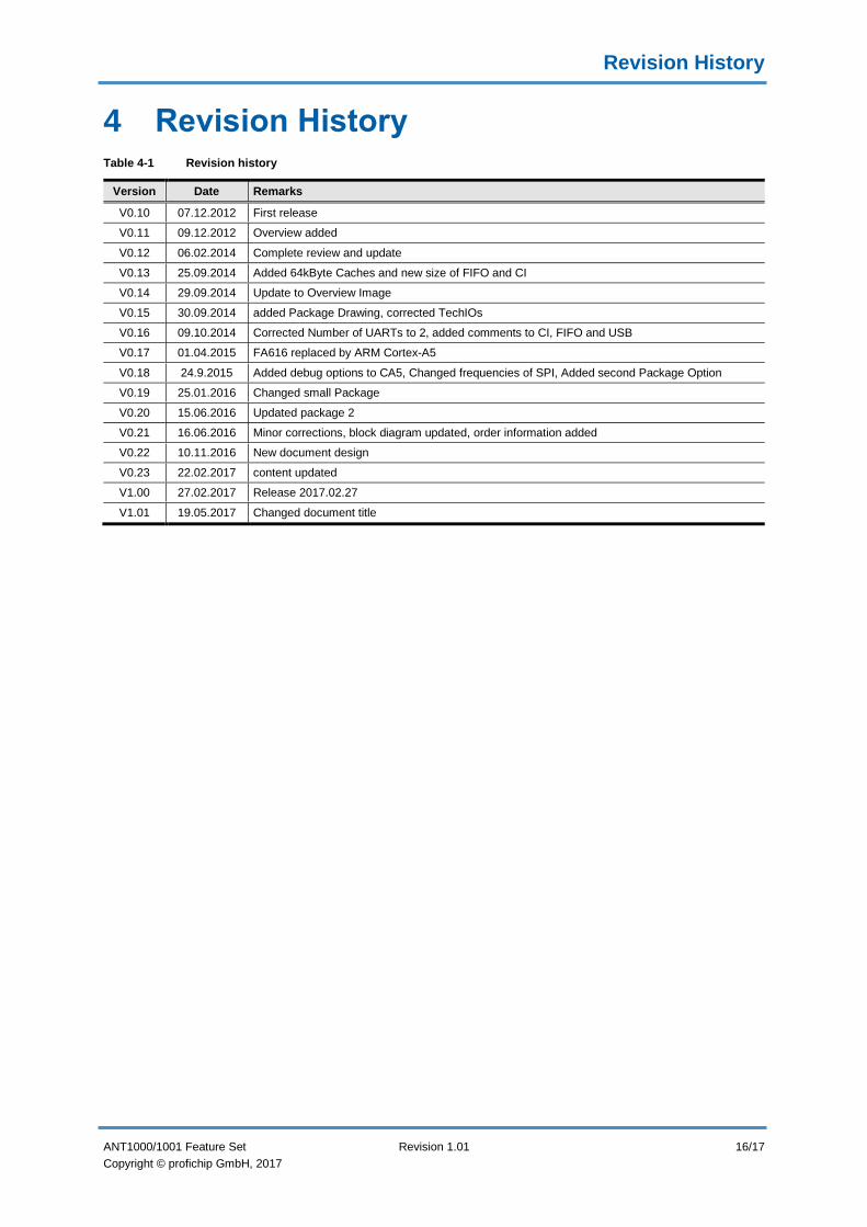
4 Revision History Table 4-1 Revision history
Version Date Remarks
V0.10 07.12.2012 First release
V0.11 09.12.2012 Overview added
V0.12 06.02.2014 Complete review and update
V0.13 25.09.2014 Added 64kByte Caches and new size of FIFO and CI
V0.14 29.09.2014 Update to Overview Image
V0.15 30.09.2014 added Package Drawing, corrected TechIOs
V0.16 09.10.2014 Corrected Number of UARTs to 2, added comments to CI, FIFO and USB
V0.17 01.04.2015 FA616 replaced by ARM Cortex-A5
V0.18 24.9.2015 Added debug options to CA5, Changed frequencies of SPI, Added second Package Option
V0.19 25.01.2016 Changed small Package
V0.20 15.06.2016 Updated package 2
V0.21 16.06.2016 Minor corrections, block diagram updated, order information added
V0.22 10.11.2016 New document design
V0.23 22.02.2017 content updated
V1.00 27.02.2017 Release 2017.02.27
V1.01 19.05.2017 Changed document title

Revision History
ANT1000/1001 Feature Set Revision 1.01 17/17
Copyright © profichip GmbH, 2017
profichip GmbH
Einsteinstrasse 6
91074 Herzogenaurach
Germany
Phone: +49.9132.744-200
Fax: +49.9132.744-2164


![[PPT]Hamming Codes - Department of Mathematicsorion.math.iastate.edu/linglong/Math690F04/HammingCodes.ppt · Web viewDecoding Extended Hamming Code q-ary Hamming Codes The binary](https://img.dokumen.tips/doc/110x75/5b373ea27f8b9aad388e1408/ppthamming-codes-department-of-web-viewdecoding-extended-hamming-code-q-ary.jpg)