Embed Size (px)
Citation preview
Annealing Accelerator for Ising Spin Systems basedon In-memory Complementary 2D FETsAmritanand Sebastian
Pennsylvania State University https://orcid.org/0000-0003-4558-0013Sarbashis Das
Pennsylvania State University https://orcid.org/0000-0003-4553-5693Saptarshi Das ( [email protected] )
Pennsylvania State University https://orcid.org/0000-0002-0188-945X
Article
Keywords:
Posted Date: April 1st, 2021
DOI: https://doi.org/10.21203/rs.3.rs-331394/v1
License: This work is licensed under a Creative Commons Attribution 4.0 International License. Read Full License

1
Annealing Accelerator for Ising Spin Systems based on In-memory
Complementary 2D FETs
Amritanand Sebastian1, Sarbashis Das2 & Saptarshi Das1,3,4*
1Deparment of Engineering Science and Mechanics, Penn State University, University Park, PA 16802
2Department of Electrical Engineering, Penn State University, University Park, PA 16802
3Department of Materials Science and Engineering, Penn State University, University Park, PA 16802
4Materials Research Institute, Pennsylvania State University, University Park, PA 16802
Abstract
Metaheuristic algorithms such as simulated annealing (SA) has been implemented for
optimization in combinatorial problems, especially for discreet problems. SA employs a
stochastic search, where high-energy transitions (“hill-climbing”) are allowed with a
temperature-dependent probability to escape local optima. Ising spin glass systems have
properties such as spin disorder and “frustration” and provide a discreet combinatorial
problem with high number of metastable states and ground-state degeneracy. In this work,
we exploit subthreshold Boltzmann transport in complementary two-dimensional (2D) field
effect transistors (p-type WSe2 and n-type MoS2) integrated with analog, non-volatile, and
programmable floating-gate memory stack to develop in-memory computing primitives
necessary for energy and area efficient hardware acceleration of SA for the Ising spin
systems. We experimentally demonstrate > 800X search acceleration for 4×4 ferromagnetic,
antiferromagnetic, and a spin glass system using SA compared to an exhaustive search using
brute force trial at miniscule total energy expenditure of ~120 nJ. Our hardware realistic
numerical simulations further highlight the astounding benefits of SA in accelerating the
search for larger spin lattices.

2
Introduction
Combinatorial optimization problems represent a set of problems where finding the best solution
using an exhaustive search is often unfeasible. Interestingly, such problems appear in applications
ranging from supply-chain management, airline scheduling, industrial resource allocation to
artificial intelligence, applied mathematics, and theoretical computer science. The travelling
salesman problem (TSP) is a representative optimization problem where given a number of cities,
the shortest route connecting all the cities must be found [1]. In TSP the time complexity is in the
order of 𝑛𝑛!, where 𝑛𝑛 is the number of cities. The optimal solution can be found for a small 𝑛𝑛 by an
exhaustive search using the brute force trial (BFT) where every combination is evaluated.
However, BFT becomes impractical for large 𝑛𝑛. For example, 40 cities would require 1049 trials!
While the BFT fails, various metaheuristic algorithms such as simulated annealing (SA) [2],
genetic algorithm [3], and ant colony optimization [4] have been utilized to obtain an approximate
solution which is very close to the actual solution for TSP and other optimization problems.
Among these, SA is an excellent optimization technique in discrete problems where multiple local
minima exist. SA provides a simple framework which can be implemented on systems with
arbitrary energy landscapes, and it statistically guarantees an optimal solution. SA has hence been
employed to solve optimization problems in a wide variety of domains such as circuit design [5],
data analysis [6], imaging [7], neural networks [8], geophysics [9], finance [10], and Ising model
of magnetism [11].
SA draws inspiration from physical annealing where a material is heated above its recrystallization
temperature to allow atoms to rearrange and is slowly cooled down to improve its crystallinity and
reach a low energy state. SA is an optimization algorithm where the free energy (𝐻𝐻) of a system
3
is minimized by employing a stochastic search. It is similar to other optimization methods such as
gradient descent [12] where transitions lowering 𝐻𝐻 are accepted. However, unlike the gradient
descent method, it allows transitions increasing 𝐻𝐻 (“hill-climbing”) determined by the annealing
temperature [13-16]. This “hill-climbing” feature of SA makes it highly attractive for systems with
multiple local minima in their energy landscape (Fig 1a). The cost associated with a state transition
leading to ∆𝐻𝐻 change in the free energy of the system is evaluated using the Boltzmann factor and
accepted if it falls below a predefined threshold, say 𝑃𝑃, following Eq. 1.
exp � ∆𝐻𝐻𝑘𝑘𝐵𝐵𝑇𝑇� < 𝑃𝑃 [1]
Here, 𝑘𝑘𝐵𝐵 is the Boltzmann constant, and 𝑇𝑇 is the temperature. This particular SA approach is also
referred to as the threshold accepting method and is widely used for its simpler structure [17]. The
basic principle of SA is illustrated in Fig. 1a. To minimize the free energy function 𝐻𝐻(𝑥𝑥)
corresponding to the argument set 𝑥𝑥 = {𝑥𝑥1, 𝑥𝑥2, 𝑥𝑥3, … 𝑥𝑥𝑁𝑁}, where 𝑁𝑁 is a large number, a random 𝑥𝑥𝑖𝑖 is initialized. At each iteration, a new random point (𝑥𝑥𝑘𝑘) is chosen and ∆𝐻𝐻 associated with the
transition is evaluated. If ∆𝐻𝐻 < 0, the transition is automatically accepted, whereas if ∆𝐻𝐻 > 0, the
transition is accepted i.e. “hill-climbing” is allowed following Eq 1. SA algorithm starts at a high 𝑇𝑇, where significant “hill-climbing” is allowed and 𝑇𝑇 is progressively reduced following an
annealing schedule. At sufficient lower 𝑇𝑇 the system finds the global minima or arrives close to
the same.
Most of the work on optimization algorithms like SA is done in software [11, 13-16], with a few
hardware demonstrations [18, 19] based on von-Neumann architecture rendering them area and
energy inefficient owing to the physical separation of memory and compute. Non-von Neumann
hardware accelerators such as graphics processing units (GPUs) [20, 21], and field-programmable

4
gate arrays (FPGAs) [22] have become increasingly popular in the later years offering speedup,
energy efficiency and smaller physical footprint [23]. Quantum annealing, a variant of SA, where
the “hill-climbing” is achieved by quantum mechanical tunneling has been implemented in D-
wave processor, a quantum computer [24]. More recently, memristive crossbar arrays have been
used to implement standalone SA [25] and SA in Hopfield neural networks for various
optimization problems [26-28]. While memristors offer in-memory computing, they have
limitations owing to sneak paths and narrow dynamic ranges limiting the number of conductance
states, high power consumption, and metal migration in the ON state due to high currents. To
improve their performance, memristors are often integrated with an access transistor in a 1T1R
structure and also require peripheral circuits based on silicon complementary metal oxide
semiconductor (CMOS) technology. Finally, annealing schedule is usually realized through
physical cooling of the system which significantly adds to the energy overhead.
In this work, we explore SA using in-memory complementary field-effect transistors (FETs) based
on ultra-thin body two-dimensional (2D) semiconductors, i.e. p-type WSe2 and n-type MoS2 FETs.
First, unlike quantum computers operating at cryogenic temperatures, our demonstration is based
on room temperature, and second, we exploit analog subthreshold conduction and analog
programmability to design unique computing primitives and annealing schedule which achieve
better energy and area efficiency compared to large memristive cross-bar arrays. Note that earlier
works have already demonstrated the scalability and technological viability of 2D materials [29-
31]. Additionally, in-memory and near-memory technologies based on 2D materials have been
used recently for various computing tasks overcoming the von-Neumann bottleneck [32-34]. This
work further advances the development of 2D FET based in-memory computing platform. To the
5
best of our knowledge this is the first demonstration of hardware acceleration of SA for the Ising
spin glass systems using emerging materials and devices.
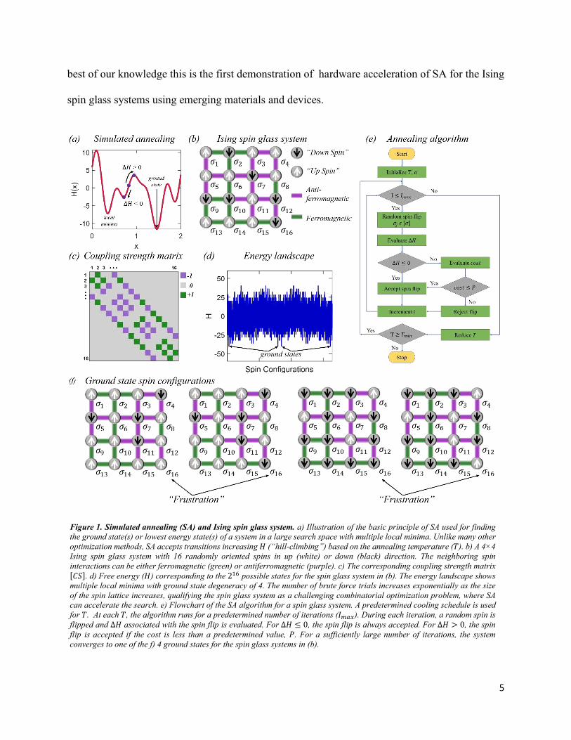
Figure 1. Simulated annealing (SA) and Ising spin glass system. a) Illustration of the basic principle of SA used for finding
the ground state(s) or lowest energy state(s) of a system in a large search space with multiple local minima. Unlike many other
optimization methods, SA accepts transitions increasing 𝐻𝐻 (“hill-climbing”) based on the annealing temperature (𝑇𝑇). b) A 4×4
Ising spin glass system with 16 randomly oriented spins in up (white) or down (black) direction. The neighboring spin
interactions can be either ferromagnetic (green) or antiferromagnetic (purple). c) The corresponding coupling strength matrix [𝐶𝐶𝐶𝐶]. d) Free energy (𝐻𝐻) corresponding to the 216 possible states for the spin glass system in (b). The energy landscape shows
multiple local minima with ground state degeneracy of 4. The number of brute force trials increases exponentially as the size
of the spin lattice increases, qualifying the spin glass system as a challenging combinatorial optimization problem, where SA
can accelerate the search. e) Flowchart of the SA algorithm for a spin glass system. A predetermined cooling schedule is used
for 𝑇𝑇. At each 𝑇𝑇, the algorithm runs for a predetermined number of iterations (𝐼𝐼𝑚𝑚𝑚𝑚𝑚𝑚). During each iteration, a random spin is
flipped and ∆𝐻𝐻 associated with the spin flip is evaluated. For ∆𝐻𝐻 ≤ 0, the spin flip is always accepted. For ∆𝐻𝐻 > 0, the spin
flip is accepted if the cost is less than a predetermined value, 𝑃𝑃. For a sufficiently large number of iterations, the system
converges to one of the f) 4 ground states for the spin glass systems in (b).
6
Spin glass system
Since the early years of SA, the Ising spin glass problem has been extensively studied since it
offers combinatorically huge number of outcomes with multiple statistically equivalent ground
states. Similar to the disordered nature of atomic positions in glass, in a spin glass system, the
magnetic spins are disordered [35, 36]. The spatial disorder in a glass is set by quenching, where
its atoms are frozen in a disordered state. Similarly, spin glass is a system of quenched magnets
with disorder due to frozen spin states and interactions. Spin glasses demonstrate interesting
properties such as frustration. At low temperatures, a spin glass system has roughly equal number
of ferromagnetic and antiferromagnetic interactions or bonds which are frozen. However, spins
can be flipped to obtain a low energy state which satisfies the frozen spin interactions. This leads
to “frustration” in spins trying to settle between competing ferromagnetic and antiferromagnetic
interactions [37]. A large number of metastable states with high degeneracy corresponding to
different spin orientations are observed in the spin glass systems. This leads to a non-monotonic
energy landscape with multiple local minima. The transition from a metastable state to the lowest
energy state requires specific spin flips and represents an optimization problem where high energy
transitions should be allowed to escape from local minima; hence, spin glass is an ideal system to
implement SA.
A 𝐾𝐾 × 𝐾𝐾 square spin lattice with 𝐾𝐾 = 4 is shown in Fig. 1b. The nature of spin interactions i.e.,
ferromagnetic (green) versus antiferromagnetic (purple) are also shown. The corresponding spin
vector [𝜎𝜎] consisting of 𝐾𝐾2 = 16 spins is given by [𝜎𝜎] = [𝜎𝜎1,𝜎𝜎2, … 𝜎𝜎𝐾𝐾2]. In the Ising spin model,
+1 represents “up” spin and -1 represents “down” spin, respectively. The Hamiltonian representing
7
the free energy of the spin glass system is given by the zero-field Edward-Anderson (EA) model
described in Eq. 2 [38].
𝐻𝐻 = − � 𝜎𝜎𝑖𝑖𝐽𝐽𝑖𝑖𝑖𝑖𝜎𝜎𝑖𝑖<𝑖𝑖,𝑖𝑖> = − 1
2�𝜎𝜎𝑖𝑖𝐽𝐽𝑖𝑖𝑖𝑖𝑁𝑁𝑖𝑖𝑖𝑖𝜎𝜎𝑖𝑖𝑖𝑖,𝑖𝑖 = −1
2�𝜎𝜎𝑖𝑖𝐶𝐶𝐶𝐶𝑖𝑖𝑖𝑖𝜎𝜎𝑖𝑖𝑖𝑖,𝑖𝑖 = − 1
2[𝜎𝜎][𝐶𝐶𝐶𝐶][𝜎𝜎]𝑇𝑇 [2]
Here, 𝜎𝜎𝑖𝑖 and 𝜎𝜎𝑖𝑖 are the 𝑖𝑖𝑡𝑡ℎ and 𝑗𝑗𝑡𝑡ℎ elements of 𝜎𝜎. 𝐽𝐽𝑖𝑖𝑖𝑖 denotes the nature of interaction between 𝜎𝜎𝑖𝑖 and 𝜎𝜎𝑖𝑖 , i.e., 𝐽𝐽𝑖𝑖𝑖𝑖 = +1 for ferromagnetic interaction and 𝐽𝐽𝑖𝑖𝑖𝑖 = -1 for antiferromagnetic interaction.
The operator <> denotes that only the nearest neighbor interactions are taken into account, i.e., 𝑁𝑁𝑖𝑖𝑖𝑖 = +1, if 𝜎𝜎𝑖𝑖 and 𝜎𝜎𝑖𝑖 are immediate neighbors and 𝑁𝑁𝑖𝑖𝑖𝑖 = 0, otherwise [25]. Note that both [𝐽𝐽] and [𝑁𝑁]
matrices are sparse matrices of size 𝐾𝐾2 × 𝐾𝐾2. These two matrices are combined into a single 𝐾𝐾2 × 𝐾𝐾2 matrix, referred to as the coupling strength matrix, [𝐶𝐶𝐶𝐶] (Fig. 1c). The light squares
represent +1, the dark squares represent -1, and the gray squares represent 0. Note that the 𝐾𝐾 × 𝐾𝐾
spin glass system with 𝐾𝐾2 number of spins, each with two possible orientations (“up”/“down”),
has 2𝐾𝐾2possible states. The free energy (𝐻𝐻) corresponding to each of these 2𝐾𝐾2states are shown in
Fig. 1d for the spin glass system shown in Fig. 1b. Clearly, the energy landscape is non-monotonic
with multiple local minima and degenerate global minima or ground states. Furthermore, with
increasing size of the spin lattice (𝐾𝐾) the search for spin configurations that satisfy all interactions
become infeasible using BFTs qualifying the spin glass system as a challenging combinatorial
optimization problem, where SA can speed-up the search process.
Simulated annealing for spin glass system
The SA algorithm to find the ground state of a spin glass system is shown in Fig. 1e. To find the
orientations of 𝐾𝐾2 = 16 spins that result in minimum free energy, a random spin in the 𝐾𝐾 × 𝐾𝐾 spin
lattice is flipped and the corresponding ∆𝐻𝐻 is evaluated using Eq. 2. If ∆𝐻𝐻 < 0, the free energy of

8
the system is lowered and hence the spin flip is accepted. However, if ∆𝐻𝐻 > 0, the spin flip
increases the free energy of the system. In this case the spin flip can still be accepted (“hill-
climbing”) if the associated cost obtained from Eq. 1 is lower than a predetermined value, 𝑃𝑃. If
both conditions are not satisfied, then the spin flip is rejected. At a given 𝑇𝑇, a predetermined
number of iterations (𝐼𝐼𝑚𝑚𝑚𝑚𝑚𝑚) are performed to traverse the energy landscape of the spin system. This
process is then repeated by progressively cooling the system i.e., by reducing 𝑇𝑇 following a
predefined cooling schedule. It is found that within a reasonable number of iterations and at a
sufficiently lower temperature the system converges to its ground state (Fig. 1f). Note that the spin
glass systems typically exhibit ground-state degeneracy. See Supplementary Fig. 1a-d for the
ground states and the free energy landscapes of 4 × 4 ferromagnetic and antiferromagnetic spin
systems, respectively. In a ferromagnetic system, the ground state degeneracy is 2 since all
interactions are satisfied if all spins are pointing “up” or “down” (Supplementary Fig. 1b). An
antiferromagnetic system also possesses ground state degeneracy of 2 since all interactions are
satisfied if adjacent spins are oriented in opposite directions (Supplementary Fig. 1d). However,
in spin glass systems, the ground-state degeneracy is increased as the ground state is unable to
satisfy all interactions due to the phenomenon of “frustration”. For example, “up” and “down”
configurations are equally valid for 𝜎𝜎16 for the spin glass system to be in its ground state (Fig. 1f).
Supplementary Video 1 shows SA for 4 × 4 ferromagnetic, antiferromagnetic, and “frustrated”
spin glass systems.
Hardware realization of simulated annealing
Hardware implementation of SA requires: 1) a random number generator for random spin flip, 2)
a computational unit to calculate the change in free energy (∆𝐻𝐻) of the spin system associated with
9
the random spin flip following Eq. 2, 3) a computational unit to determine the cost of “hill-
climbing” if ∆𝐻𝐻 > 0 to accept or reject the spin flip following Eq. 1, and finally 4) a hardware
mechanism equivalent to the annealing schedule or cooling in metallurgy. While we use software
code to generate the random numbers, all other computational units including the mechanism for
annealing are realized in hardware. For example, a multiplier module is designed using
complementary 2D FETs along with a resistor and a capacitor module to evaluate ∆𝐻𝐻. Similarly,
co-location of analog memory and analog computing enabled by non-volatile and programmable
floating-gate MoS2 FETs is used to determine the cost of “hill-climbing” and achieve an annealing
schedule equivalent to changing the 𝑇𝑇 .
The schematic and optical image of a back-gated p-type WSe2 FET with 50 𝑛𝑛𝑛𝑛 Al2O3 as the gate
dielectric is shown in Fig. 2a-b, respectively. Undoped WSe2 demonstrates ambipolar transport
with both electron (n-type) and hole (p-type) conduction owing to the pinning of metal Fermi-level
near the middle of the WSe2 bandgap [39-41]. However, for the design of the multiplier module,
unipolar p-type WSe2 is preferred. Hence, WSe2 is doped p-type using surface charge transfer
doping with sub-stochiometric WO3-x [40]. Doping is achieved on a multilayered WSe2 flake by
converting its top layers to WO3-x by exposure to mild O2 plasma as discussed in our earlier reports
[40, 42]. As shown in Fig. 2a before O2 plasma exposure, the flakes are patterned to obtain a p-i-
p structure i.e., p-doped source and drain extension regions with the middle region left intrinsic
[40] (see Methods section for details on p-type WSe2 FET fabrication). The length of the intrinsic
region is designed to be 500 𝑛𝑛𝑛𝑛. The corresponding transfer characteristics, i.e., drain current
(𝐼𝐼DS) versus back-gate voltage (𝑉𝑉BG) for different drain-to-source voltage (𝑉𝑉DS) and output
characteristics, i.e., 𝐼𝐼DS versus 𝑉𝑉DS for different 𝑉𝑉BG of the WSe2 FET are shown in in Fig. 2c-d,
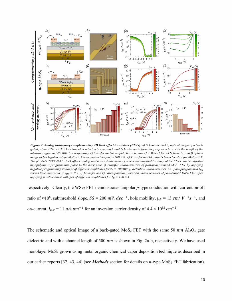
10
respectively. Clearly, the WSe2 FET demonstrates unipolar p-type conduction with current on-off
ratio of ≈108, subthreshold slope, 𝐶𝐶𝐶𝐶 = 200 𝑛𝑛𝑉𝑉.𝑑𝑑𝑑𝑑𝑑𝑑−1, hole mobility, µ𝑃𝑃 = 13 𝑑𝑑𝑛𝑛2 𝑉𝑉−1𝑠𝑠−1, and
on-current, 𝐼𝐼𝑂𝑂𝑁𝑁 = 11 𝜇𝜇𝜇𝜇. 𝜇𝜇𝑛𝑛−1 for an inversion carrier density of 4.4 × 10¹² 𝑑𝑑𝑛𝑛−2.
The schematic and optical image of a back-gated MoS2 FET with the same 50 𝑛𝑛𝑛𝑛 Al2O3 gate
dielectric and with a channel length of 500 𝑛𝑛𝑛𝑛 is shown in Fig. 2a-b, respectively. We have used
monolayer MoS2 grown using metal organic chemical vapor deposition technique as described in
our earlier reports [32, 43, 44] (see Methods section for details on n-type MoS2 FET fabrication).
Figure 2. Analog in-memory complementary 2D field effect transistors (FETs). a) Schematic and b) optical image of a back-
gated p-type WSe2 FET. The channel is selectively exposed to mild O2 plasma to form the p-i-p structure with the length of the
intrinsic region as 500 𝑛𝑛𝑛𝑛. Corresponding c) transfer and d) output characteristics for WSe2 FET. e) Schematic and f) optical
image of back-gated n-type MoS2 FET with channel length as 500 𝑛𝑛𝑛𝑛. g) Transfer and h) output characteristics for MoS2 FET.
The p++-Si/TiN/Pt/Al2O3 stack offers analog and non-volatile memory where the threshold voltage of the FETs can be adjusted
by applying a programming pulse to the back gate. i) Transfer characteristics of post-programmed MoS2 FET by applying
negative programming voltages of different amplitudes for 𝑡𝑡𝑃𝑃 = 100 𝑛𝑛𝑠𝑠. j) Retention characteristics, i.e., post-programmed 𝐼𝐼𝐷𝐷𝐷𝐷
versus time measured at 𝑉𝑉𝐵𝐵𝐵𝐵 = 0 𝑉𝑉. i) Transfer and k) corresponding retention characteristics of post-erased MoS2 FET after
applying positive erase voltages of different amplitudes for 𝑡𝑡𝐸𝐸 = 100 𝑛𝑛𝑠𝑠.

11
For MoS2, the metal Fermi-level pins closer to the conduction band at the source/drain contact
interfaces resulting in unipolar n-type conduction [41, 45]. The corresponding transfer
characteristics and output characteristics are shown in Fig. 2c-d, respectively. For monolayer MoS2
FET, we extracted current on-off ratio of ≈107, subthreshold slope, 𝐶𝐶𝐶𝐶 = 310 𝑛𝑛𝑉𝑉.𝑑𝑑𝑑𝑑𝑑𝑑−1, electron
mobility, µ𝑁𝑁= 15 𝑑𝑑𝑛𝑛2 𝑉𝑉−1𝑠𝑠−1, and 𝐼𝐼𝑂𝑂𝑁𝑁 = 6.7 𝜇𝜇𝜇𝜇. 𝜇𝜇𝑛𝑛−1 for an inversion carrier density of 3.7 ×
1012 𝑑𝑑𝑛𝑛−2.
The unique stack of p++ Si/TiN/Pt/Al2O3 offers analog and non-volatile memory, i.e. the threshold
voltage of the FETs can be adjusted by applying a programming voltage (𝑉𝑉P) to the back-gate
electrode for a programming pulse time (𝑡𝑡P). The programmability is shown in Fig. 2e using the
transfer characteristics of a MoS2 FET at 𝑉𝑉DS = 1 𝑉𝑉 after the application of negative programming
voltages of different amplitudes for 𝑡𝑡P = 100 𝑛𝑛𝑠𝑠. Fig. 2f shows the retention characteristics, i.e.
post-programmed 𝐼𝐼DS versus time measured at 𝑉𝑉BG = 2 𝑉𝑉 confirming non-volatile and analog
programmability of the MoS2 FET. Similarly, by applying positive erase voltages (𝑉𝑉E) for an erase
pulse time, 𝑡𝑡E = 100 𝑛𝑛𝑠𝑠, the programmed states can be erased and the transfer characteristics can
be shifted in the opposite direction as shown in Fig. 2g. The corresponding non-volatile retention
characteristics are shown in Fig. 2h. Note that, programming (erase) operation can also be achieved
by varying 𝑡𝑡P (𝑡𝑡E) for a fixed 𝑉𝑉P (𝑉𝑉E) as shown in Supplementary Fig. 2a and 2b. The working
principle of the analog and non-volatile back-gate memory stack has been described in detail in
our earlier report [32].
The above demonstration of p-type WSe2 FET, n-type MoS2 FET, and the analog compute and
analog non-volatile storage capability allow us to design the computational primitives necessary

12
for the hardware realization of SA. Note that 𝛥𝛥𝐻𝐻 due to random spin flip event can be computed
from the difference in the free energy of the spin glass system before (𝐻𝐻) and after (𝐻𝐻′) the spin
flip. According to Eq. 2, evaluation of 𝐻𝐻 and 𝐻𝐻′ require multiplication of the spin vector [𝜎𝜎] of
size 1 × 𝐾𝐾2 with the [𝐶𝐶𝐶𝐶] matrix of size 𝐾𝐾2 × 𝐾𝐾2 followed by multiplication with the transpose
of the spin vector, i.e., [𝜎𝜎]𝑇𝑇 of size 𝐾𝐾2 × 1. However, there are several challenges: first, while
vector matrix multiplication can be realized using cross-bar architectures, the [𝐶𝐶𝐶𝐶] matrix contains
negative elements which is difficult to realize using conductance states and requires additional
circuitry (note that earlier demonstration of SA [25] using resistive random access memory only
implemented ferroelectric interactions); and second, the size of the [𝐶𝐶𝐶𝐶] matrix can become
substantial even for relatively low values of 𝐾𝐾 imposing heavy area and energy overhead for the
computation. Instead, the computational load can be significantly reduced by acknowledging the
fact that only one spin is allowed to randomly flip during each iteration of SA, simplifying the
computation of ∆𝐻𝐻 following Eq. 3
𝛥𝛥𝐻𝐻 = 𝐻𝐻′ − 𝐻𝐻 = �− 1
2�𝐶𝐶𝐶𝐶𝑖𝑖𝑖𝑖𝜎𝜎𝑖𝑖𝜎𝜎𝑖𝑖′𝑖𝑖,𝑖𝑖 � − �−1
2�𝐶𝐶𝐶𝐶𝑖𝑖𝑖𝑖𝜎𝜎𝑖𝑖𝜎𝜎𝑖𝑖𝑖𝑖,𝑖𝑖 � = �− 1
2𝛥𝛥𝜎𝜎𝑖𝑖� ��𝐶𝐶𝐶𝐶𝑖𝑖𝑖𝑖𝜎𝜎𝑖𝑖𝐾𝐾2
𝑖𝑖=1 � [3]
Here, we assume that the 𝑗𝑗𝑡𝑡ℎ spin is flipped. Note that the first term inside the square bracket, i.e., �− 12𝛥𝛥𝜎𝜎𝑖𝑖� is computationally equivalent to the initial spin state of 𝜎𝜎𝑖𝑖 . For example, if 𝜎𝜎𝑖𝑖 flips from
+1(-1) to -1(+1), 𝛥𝛥𝜎𝜎𝑖𝑖 = -2(+2) and hence �− 12𝛥𝛥𝜎𝜎𝑖𝑖� = +1(-1). Therefore, following Eq. 3, 𝛥𝛥𝐻𝐻 can
be obtained just by summing the result of the dot product of the spin vector [𝜎𝜎] with the 𝑗𝑗𝑡𝑡ℎ row
vector of the [𝐶𝐶𝐶𝐶] matrix, i.e., [𝐶𝐶𝐶𝐶]𝑖𝑖 and by multiplying the sum with 𝜎𝜎𝑖𝑖 . Fig. 3a-d show the circuit
modules used for computing 𝛥𝛥𝐻𝐻. The multiplication module (M1) in Fig. 3a comprises of a WSe2
FET (T1) and MoS2 FET (T2), connected in series with a common gate and a common source
terminal. It multiplies the sign of two input voltages, 𝑉𝑉in−1 and 𝑉𝑉in−2. 𝑉𝑉𝑖𝑖𝑖𝑖−1 is applied to the

13
Figure 3. Circuit modules for hardware acceleration of SA. a) The multiplier module (M1) has a p-type WSe2 FET (T1) and
an n-type MoS2 FET (T2), connected in series with a common gate and a common source terminal. It multiplies the sign of two
input voltages, 𝑉𝑉𝑖𝑖𝑖𝑖−1 and 𝑉𝑉𝑖𝑖𝑖𝑖−2. 𝑉𝑉𝑖𝑖𝑖𝑖−1 is applied to the common-gate terminal, 𝑉𝑉𝑖𝑖𝑖𝑖−2 is applied to the drain terminal of T1, and −𝑉𝑉𝑖𝑖𝑖𝑖−2 is applied to the drain terminal of T2. b) Transfer characteristic of T1 and T2. c) Transfer characteristics of M1 i.e.,
output voltage, 𝑉𝑉𝑜𝑜𝑜𝑜𝑡𝑡 versus 𝑉𝑉𝑖𝑖𝑖𝑖−1 for 𝑉𝑉𝑖𝑖𝑖𝑖−2 = ±0.1 V. Using M1 the product between the 𝑖𝑖𝑡𝑡ℎ elements of [𝜎𝜎] and [𝐶𝐶𝐶𝐶]𝑖𝑖 is obtained at the 𝑖𝑖𝑡𝑡ℎ time step (𝑖𝑖𝑖𝑖𝑝𝑝) as 𝑉𝑉𝑜𝑜𝑜𝑜𝑡𝑡(𝑖𝑖𝑖𝑖𝑝𝑝) by applying, 𝑉𝑉𝑖𝑖𝑖𝑖−1(𝑖𝑖𝑖𝑖𝑝𝑝) = 𝑉𝑉1𝜎𝜎𝑖𝑖 and 𝑉𝑉𝑖𝑖𝑖𝑖−2�𝑖𝑖𝑖𝑖𝑝𝑝� = 𝑉𝑉2𝐶𝐶𝐶𝐶𝑖𝑖𝑖𝑖. Note that 𝑖𝑖 = 1:1:𝐾𝐾2, 𝐾𝐾 = 4. We have used 𝑖𝑖𝑝𝑝 =60 ms, 𝑉𝑉1 = 1 V, and 𝑉𝑉2 = 0.1 V resulting in 𝑉𝑉𝑜𝑜𝑜𝑜𝑡𝑡(𝑖𝑖𝑖𝑖𝑝𝑝) = 0.1×𝐶𝐶𝐶𝐶𝑖𝑖𝑖𝑖𝜎𝜎𝑖𝑖. d) The voltage to current
converter module (M2) transforms 𝑉𝑉𝑜𝑜𝑜𝑜𝑡𝑡 from M1 into current, 𝐼𝐼𝑜𝑜𝑜𝑜𝑡𝑡 following 𝐼𝐼𝑜𝑜𝑜𝑜𝑡𝑡 = 𝐺𝐺𝑉𝑉𝑜𝑜𝑜𝑜𝑡𝑡 with 𝐺𝐺 ≈ 0.5 µS. e) The integrator module (M3), a capacitor (𝐶𝐶𝐼𝐼 = 20 nF), sums 𝐼𝐼𝑜𝑜𝑜𝑜𝑡𝑡 from M2 over 𝐾𝐾2 time steps into voltage, VΔH. f) 𝑉𝑉𝑖𝑖𝑖𝑖−1, 𝑉𝑉𝑖𝑖𝑖𝑖−2, −𝑉𝑉𝑖𝑖𝑖𝑖−2, 𝑉𝑉𝑜𝑜𝑜𝑜𝑡𝑡, 𝐼𝐼𝑜𝑜𝑜𝑜𝑡𝑡, and the output from M3, i.e., 𝑉𝑉𝐼𝐼 for representative ferromagnetic, antiferromagnetic, and a spin glass system during a
given iteration of SA. 𝑉𝑉∆𝐻𝐻 and 𝜎𝜎𝑖𝑖 are multiplied to obtain 𝛥𝛥𝐻𝐻. g) Schematic and h) transfer characteristics of a programmable
MoS2 FET used for evaluating the cost associated with the state transition as well as for realizing cooling schedule in hardware.
The subthreshold conduction governed by Boltzmann statistics is exploited to evaluate the cost of “hill-climbing” by applying 𝑉𝑉𝐵𝐵𝐵𝐵 = 𝛥𝛥𝐻𝐻 and the spin flip is accepted if 𝐼𝐼∆𝐻𝐻 < 𝐼𝐼𝑐𝑐𝑜𝑜𝑐𝑐𝑡𝑡 = 100 𝑝𝑝𝜇𝜇. The cooling schedule is implemented by shifting the threshold
voltage of the FET through back-gate programming.

14
common-gate terminal, 𝑉𝑉𝑖𝑖𝑖𝑖−2 is applied to the drain terminal of T1, and −𝑉𝑉𝑖𝑖𝑖𝑖−2 is applied to the
drain terminal of T2. Note that, T1 and T2 demonstrate dominant p-type and n-type conduction,
respectively, as shown in Fig. 3e. The transfer characteristics of M1, i.e., output voltage, 𝑉𝑉𝑜𝑜𝑜𝑜𝑡𝑡 versus 𝑉𝑉𝑖𝑖𝑖𝑖−1 for 𝑉𝑉𝑖𝑖𝑖𝑖−2 = ±0.1 V are shown in Fig. 3f. For 𝑉𝑉𝑖𝑖𝑖𝑖−1 = 1 V, 𝑉𝑉𝑜𝑜𝑜𝑜𝑡𝑡 = 𝑉𝑉𝑖𝑖𝑖𝑖−2, whereas for 𝑉𝑉𝑖𝑖𝑖𝑖−1 = -1 V, 𝑉𝑉𝑜𝑜𝑜𝑜𝑡𝑡 = −𝑉𝑉𝑖𝑖𝑖𝑖−2. This is expected since for 𝑉𝑉𝑖𝑖𝑖𝑖−1 = 1 V, the n-type MoS2 FET (T2) is
more conductive than the p-type WSe2 FET (T1) allowing 𝑉𝑉𝑜𝑜𝑜𝑜𝑡𝑡 to follow 𝑉𝑉𝑖𝑖𝑖𝑖−2 and vice versa for 𝑉𝑉𝑖𝑖𝑖𝑖−1 = -1 V (Fig. 3e). Using M1 the product between the 𝑖𝑖𝑡𝑡ℎ elements of [𝜎𝜎] and [𝐶𝐶𝐶𝐶]𝑖𝑖 is obtained
at the 𝑖𝑖𝑡𝑡ℎ time step (𝑖𝑖𝑖𝑖𝑝𝑝) as 𝑉𝑉𝑜𝑜𝑜𝑜𝑡𝑡(𝑖𝑖𝑖𝑖𝑝𝑝) by applying, 𝑉𝑉𝑖𝑖𝑖𝑖−1(𝑖𝑖𝑖𝑖𝑝𝑝) = 𝑉𝑉1𝜎𝜎𝑖𝑖 and 𝑉𝑉𝑖𝑖𝑖𝑖−2�𝑖𝑖𝑖𝑖𝑝𝑝� = 𝑉𝑉2𝐶𝐶𝐶𝐶𝑖𝑖𝑖𝑖. We have used 𝑖𝑖𝑝𝑝 =60 ms, 𝑉𝑉1 = 1 V, and 𝑉𝑉2 = 0.1 V resulting in 𝑉𝑉𝑜𝑜𝑜𝑜𝑡𝑡(𝑖𝑖𝑖𝑖𝑝𝑝) = 0.1×𝐶𝐶𝐶𝐶𝑖𝑖𝑖𝑖𝜎𝜎𝑖𝑖. Next 𝑉𝑉𝑜𝑜𝑜𝑜𝑡𝑡 is converted to 𝐼𝐼𝑜𝑜𝑜𝑜𝑡𝑡 using a voltage to current converter module, M2 (Fig. 3b), comprising of a
resistor, following 𝐼𝐼𝑜𝑜𝑜𝑜𝑡𝑡 = 𝐺𝐺𝑉𝑉𝑜𝑜𝑜𝑜𝑡𝑡 with 𝐺𝐺 ≈ 0.5 µS. Finally, the contribution due to all spins are
summed over 𝐾𝐾2 time steps using an integrator module, M3 (Fig. 3c), comprising of a capacitor
(𝐶𝐶𝐼𝐼 ≈ 20 nF) resulting in 𝑉𝑉∆𝐻𝐻 given by Eq. 4.
𝑉𝑉∆𝐻𝐻 = 𝑖𝑖𝑝𝑝𝐶𝐶𝐼𝐼�𝐼𝐼𝑜𝑜𝑜𝑜𝑡𝑡(𝑖𝑖)𝐾𝐾2
𝑖𝑖=1 =𝑖𝑖𝑝𝑝𝐶𝐶𝐼𝐼 𝐺𝐺𝑉𝑉2�𝐶𝐶𝐶𝐶𝑖𝑖𝑖𝑖𝜎𝜎𝑖𝑖𝐾𝐾2
𝑖𝑖=1 [4]
Fig. 3g shows 𝑉𝑉𝑖𝑖𝑖𝑖−1, 𝑉𝑉𝑖𝑖𝑖𝑖−2, −𝑉𝑉𝑖𝑖𝑖𝑖−2, 𝑉𝑉𝑜𝑜𝑜𝑜𝑡𝑡, 𝐼𝐼𝑜𝑜𝑜𝑜𝑡𝑡, and the output of the integrator, 𝑉𝑉𝐼𝐼 for representative
ferromagnetic, antiferromagnetic, and spin glass systems during a given iteration. Finally, 𝑉𝑉∆𝐻𝐻 and 𝜎𝜎𝑖𝑖 are multiplied to obtain 𝛥𝛥𝐻𝐻.
Following the evaluation of 𝛥𝛥𝐻𝐻, it must be determined if the spin flip is accepted. Traditionally,
this is done using two separate steps: one to determine the sign of 𝛥𝛥𝐻𝐻 and another one to determine
the cost of “hill-climbing” if 𝛥𝛥𝐻𝐻 is positive. In hardware, both steps are combined in M4 (Fig. 3d)
by exploiting the subthreshold conduction in an FET where the carrier injection from the source

15
contact into the semiconducting channel is given by Boltzmann statistics. The cost of “hill-
climbing” is, therefore, obtained by applying 𝑉𝑉𝐵𝐵𝐵𝐵 = 𝛥𝛥𝐻𝐻 and the spin flip is accepted if 𝐼𝐼∆𝐻𝐻 < 𝐼𝐼𝑐𝑐𝑜𝑜𝑐𝑐𝑡𝑡 = 100 𝑝𝑝𝜇𝜇 (Fig. 3h) following Eq. 5.
𝐼𝐼∆𝐻𝐻 = 𝐼𝐼0 exp �− 𝑞𝑞𝛥𝛥𝐻𝐻𝑛𝑛𝑘𝑘𝐵𝐵𝑇𝑇� [5]
Here, 𝑞𝑞 is the electronic charge, 𝐼𝐼0 is the static leakage current, and 𝑛𝑛 is the body factor, which
determines the 𝐶𝐶𝐶𝐶 following Eq 6.
𝐶𝐶𝐶𝐶 =𝑛𝑛𝑘𝑘𝐵𝐵𝑇𝑇𝑞𝑞 𝑙𝑙𝑛𝑛(10); 𝑛𝑛 = �1 +
𝐶𝐶𝐷𝐷𝐶𝐶𝑂𝑂𝑂𝑂 +𝐶𝐶𝐼𝐼𝑇𝑇𝐶𝐶𝑂𝑂𝑂𝑂� [6]
Here, 𝐶𝐶𝐷𝐷 is the semiconductor capacitance, 𝐶𝐶𝐼𝐼𝑇𝑇 is the interface trap capacitance, and 𝐶𝐶𝑂𝑂𝑂𝑂 is the
oxide capacitance. For fully depleted ultra-thin-body FETs, 𝐶𝐶𝐷𝐷 = 0. We extracted 𝐶𝐶𝐶𝐶 of 430 𝑛𝑛𝑉𝑉.𝑑𝑑𝑑𝑑𝑑𝑑−1 and hence 𝑛𝑛 of 7.1. Note that in Fig. 3h the transfer characteristics is represented as a
plot of 𝐼𝐼∆𝐻𝐻 versus 𝛥𝛥𝐻𝐻. Also note that all negative 𝛥𝛥𝐻𝐻 (low-energy transition) naturally leads to 𝐼𝐼∆𝐻𝐻
< 𝐼𝐼𝑐𝑐𝑜𝑜𝑐𝑐𝑡𝑡, whereas, positive 𝛥𝛥𝐻𝐻 up to 𝛥𝛥𝐻𝐻max satisfies the “hill-climbing” criterion of 𝐼𝐼∆𝐻𝐻 < 𝐼𝐼𝑐𝑐𝑜𝑜𝑐𝑐𝑡𝑡.
Next, we implement cooling schedule in hardware. While temperature can be used to the change
the current 𝐼𝐼∆𝐻𝐻 for same 𝛥𝛥𝐻𝐻 following Eq. 5, physically changing the temperature of a system
requires excessive energy. Alternatively, 𝛥𝛥𝐻𝐻max can be modulated by programming the MoS2 FET
in different states as shown in Fig. 3h. As the annealing temperature is lowered, the transfer
characteristics is shifted towards the left. This ensures acceptance of more positive 𝛥𝛥𝐻𝐻 at higher
temperature and no “hill climbing” at T = 0 K, i.e. 𝛥𝛥𝐻𝐻max = 0 V. As shown in Fig. 3h, our
annealing schedule involved five (5) different 𝛥𝛥𝐻𝐻max = 0.6 𝑉𝑉, 0.45 𝑉𝑉, 0.3 𝑉𝑉, 0.15 𝑉𝑉, and 0 𝑉𝑉
analogous to temperature in metallurgical annealing with maximum number of iteration, 𝐼𝐼max = 5,
15, 15, 30, and 30 at the respective “temperatures”.

16
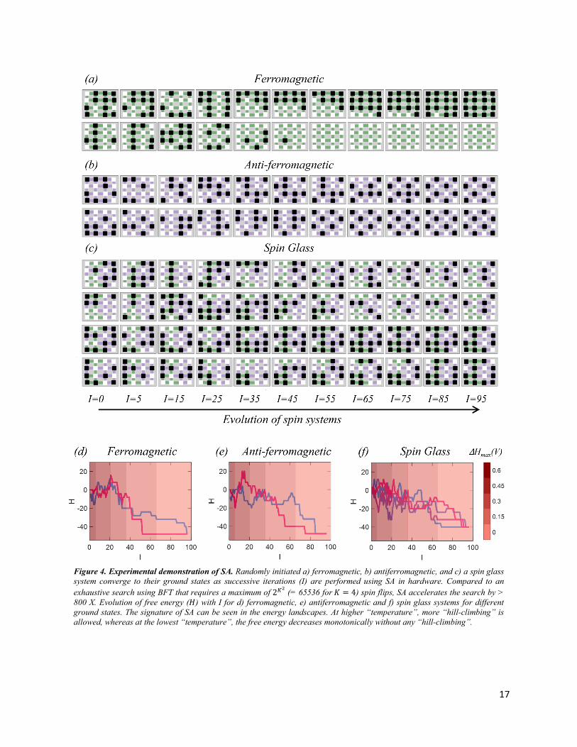
Fig. 4a-c, respectively, show the representative experimental demonstration of SA leading to the
convergence of randomly initiated ferromagnetic, antiferromagnetic, and a spin glass system to
their respective ground states. See Supplementary Figures 3-5 and Supplementary Video 2-4 for
SA experiments performed on ferromagnetic, antiferromagnetic and a spin glass system initiated
with 20 randomly oriented spin configurations. 11 ferromagnetic (55%), 9 antiferromagnetic
(45%) and 8 spin glass systems (40%) converged and reached their respective ground states at the
end of the total 95 iterations. Additionally, multiple systems are either 1 or 2 spin flips away from
their ground state, and hence they are expected to converge for an increased number of iterations.
We also observed “frustration” in the spin glass system. Remarkably, compared to an exhaustive
search using BFT that requires a maximum of 2𝐾𝐾2 (= 65536 for 𝐾𝐾 = 4) spin flips, SA accelerates
the search requiring orders of magnitude lower spin flip events. We define acceleration as the ratio
of maximum number of spin flips using exhaustive search to the maximum number of SA spin
flips to reach the ground state. The highest acceleration for ferromagnetic, antiferromagnetic and
the spin glass system were found to be ~1365X, ~1260X, and ~1310X, respectively, whereas, the
average acceleration for the systems that converged to their ground states were ~850X, ~900X,
and ~810X, respectively. Evolution of the free energy (𝐻𝐻) for representative ferromagnetic,
antiferromagnetic, and spin glass systems are shown in Fig. 4d-f, respectively (see Supplementary
Figures 6 for the evolution 𝐻𝐻 for all 60 spin systems used in our experiments). The signature of
SA can be seen in the energy landscapes, i.e. significant “hill-climbing” occurs during the initial
iterations when the system is at higher “temperature”, whereas at the lowest “temperature”, the
free energy decreases monotonically.
17
Figure 4. Experimental demonstration of SA. Randomly initiated a) ferromagnetic, b) antiferromagnetic, and c) a spin glass
system converge to their ground states as successive iterations (I) are performed using SA in hardware. Compared to an
exhaustive search using BFT that requires a maximum of 2𝐾𝐾2 (= 65536 for 𝐾𝐾 = 4) spin flips, SA accelerates the search by >
800 X. Evolution of free energy (𝐻𝐻) with I for d) ferromagnetic, e) antiferromagnetic and f) spin glass systems for different
ground states. The signature of SA can be seen in the energy landscapes. At higher “temperature”, more “hill-climbing” is
allowed, whereas at the lowest “temperature”, the free energy decreases monotonically without any “hill-climbing”.

18
To obtain further insight, hardware-realistic simulation of SA is performed using the virtual source
(VS) model developed in our earlier work to capture the 2D FET characteristics [46, 47]. Fig. 5a-
c, respectively, show the convergence accuracy of 1000 randomly initiated 4×4 ferromagnetic,
antiferromagnetic, and a spin glass system subjected to SA for different total number of iterations
(𝐼𝐼). All ferromagnetic and antiferromagnetic systems converged after ~600 and ~750 iterations
resulting in average acceleration of ~110X and ~90X, respectively, compared to exhaustive BFTs.
Note that these average acceleration numbers are lower than the experimental findings since more
iterations are performed (200 at each temperature) at higher temperatures. The spin glass system,
however, shows ~80% convergence accuracy after ~700 iterations. This is owing to the fact that
any spin glass system is more prone to getting stuck in a metastable state. Fig. 5d shows the
convergence accuracy for 100 randomly oriented 𝐾𝐾× 𝐾𝐾 ferromagnetic spin systems as a function
Figure 5. Hardware-realistic simulation of SA using virtual source model. Convergence accuracy of 1000 randomly initiated
4×4 a) ferromagnetic, b) antiferromagnetic, and a c) spin glass system subjected to SA for different total number of iterations
(𝐼𝐼). d) Convergence accuracy for 100 randomly oriented 𝐾𝐾× 𝐾𝐾 ferromagnetic spin systems as a function of total number of
spins (𝐾𝐾2) and total number of SA iterations. e) Acceleration factor i.e., the ratio of maximum number of spin flips using brute
force trail to the maximum number of SA spin flips for 100% convergence accuracy as a function of 𝐾𝐾2.

19
of total number of spins (𝐾𝐾2) and total number of SA iterations. Even for 𝐾𝐾 = 10, SA requires
only ~ 3500 iterations or maximum number of spin flips in comparison to ~1030 maximum number
of spin flips required for an exhaustive search demonstrating the tremendous improvement in
acceleration (~ 1026X). Fig. 5e shows the acceleration for ~100% convergence accuracy as a
function of 𝐾𝐾2. Clearly, as 𝐾𝐾 increases the benefits of SA becomes even more astounding.
Finally, we evaluate the energy expenditure (𝐸𝐸𝐷𝐷𝑆𝑆) by our annealing accelerator during each
iteration following Eq. 7. 𝐸𝐸𝐷𝐷𝑆𝑆 = 𝐸𝐸𝑀𝑀1 + 𝐸𝐸𝑀𝑀2 + 𝐸𝐸𝑀𝑀3 + 𝐸𝐸𝑀𝑀4
= ���(𝐼𝐼T1 + 𝐼𝐼T2)𝑉𝑉𝑖𝑖𝑖𝑖−2𝑖𝑖𝑝𝑝�𝑀𝑀1 + �𝐼𝐼out𝑉𝑉𝑜𝑜𝑜𝑜𝑡𝑡𝑖𝑖𝑝𝑝�𝑀𝑀2 + �12𝐶𝐶(∆𝑉𝑉𝐼𝐼)2�𝑀𝑀3�𝐾𝐾2
𝑖𝑖=1 + �𝐼𝐼∆𝐻𝐻𝑉𝑉𝐷𝐷𝐷𝐷𝑖𝑖𝑝𝑝�𝑀𝑀4 [7]
Here, 𝐸𝐸𝑀𝑀1, 𝐸𝐸𝑀𝑀2, 𝐸𝐸𝑀𝑀3, and 𝐸𝐸𝑀𝑀4 are the energy consumption by M1, M2, M3, and M4, respectively,
and 𝐼𝐼T1 and 𝐼𝐼T2 are the current in T1 and T2, respectively. Supplementary Fig. 7 shows 𝐸𝐸𝑀𝑀1, 𝐸𝐸𝑀𝑀2, 𝐸𝐸𝑀𝑀3, 𝐸𝐸𝑀𝑀4, and 𝐸𝐸𝐷𝐷𝑆𝑆 averaged over all 60 spin systems as a function of 𝐼𝐼 for 4×4 spin lattice. The
average energy expenditure for the hardware module was found to be miniscule ~1.3 nJ/iteration,
which corresponds to maximum total energy expenditure of ~120 nJ for finding the ground state
of any 4×4 spin system. Note that due to the limitations imposed by our measurement instruments,
we have used 𝑖𝑖𝑝𝑝 = 60 ms. However, it is possible to scale 𝑖𝑖𝑝𝑝 and thereby reduce the energy
expenditure even further. Also note that our energy calculations exclude the software operations
performed using MATLAB such as the generation of random numbers.

20
Conclusion
This work successfully demonstrates hardware acceleration of SA for the Ising spin system by
exploiting subthreshold conduction and analog programmability of complementary 2D FETs
integrated with non-volatile floating-gate memory stack. By designing in-memory computing
primitives and annealing schedule equivalent of cooling, we were able to achieve > 800X
acceleration for 4×4 ferromagnetic, antiferromagnetic, and a spin glass system, experimentally, at
frugal average energy expenditure of ~ 120 nJ. Our numerical simulations show more striking
benefits of SA for search acceleration of larger spin lattices.
21
Methods
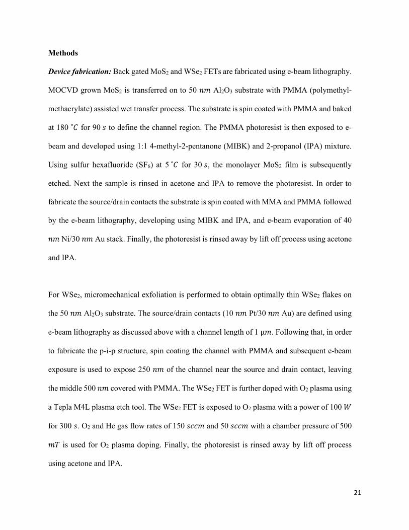
Device fabrication: Back gated MoS2 and WSe2 FETs are fabricated using e-beam lithography.
MOCVD grown MoS2 is transferred on to 50 𝑛𝑛𝑛𝑛 Al2O3 substrate with PMMA (polymethyl-
methacrylate) assisted wet transfer process. The substrate is spin coated with PMMA and baked
at 180 ˚𝐶𝐶 for 90 𝑠𝑠 to define the channel region. The PMMA photoresist is then exposed to e-
beam and developed using 1:1 4-methyl-2-pentanone (MIBK) and 2-propanol (IPA) mixture.
Using sulfur hexafluoride (SF6) at 5 ˚𝐶𝐶 for 30 𝑠𝑠, the monolayer MoS2 film is subsequently
etched. Next the sample is rinsed in acetone and IPA to remove the photoresist. In order to
fabricate the source/drain contacts the substrate is spin coated with MMA and PMMA followed
by the e-beam lithography, developing using MIBK and IPA, and e-beam evaporation of 40 𝑛𝑛𝑛𝑛 Ni/30 𝑛𝑛𝑛𝑛 Au stack. Finally, the photoresist is rinsed away by lift off process using acetone
and IPA.
For WSe2, micromechanical exfoliation is performed to obtain optimally thin WSe2 flakes on
the 50 𝑛𝑛𝑛𝑛 Al2O3 substrate. The source/drain contacts (10 𝑛𝑛𝑛𝑛 Pt/30 𝑛𝑛𝑛𝑛 Au) are defined using
e-beam lithography as discussed above with a channel length of 1 µ𝑛𝑛. Following that, in order
to fabricate the p-i-p structure, spin coating the channel with PMMA and subsequent e-beam
exposure is used to expose 250 𝑛𝑛𝑛𝑛 of the channel near the source and drain contact, leaving
the middle 500 𝑛𝑛𝑛𝑛 covered with PMMA. The WSe2 FET is further doped with O2 plasma using
a Tepla M4L plasma etch tool. The WSe2 FET is exposed to O2 plasma with a power of 100 𝑊𝑊
for 300 𝑠𝑠. O2 and He gas flow rates of 150 𝑠𝑠𝑑𝑑𝑑𝑑𝑛𝑛 and 50 𝑠𝑠𝑑𝑑𝑑𝑑𝑛𝑛 with a chamber pressure of 500 𝑛𝑛𝑇𝑇 is used for O2 plasma doping. Finally, the photoresist is rinsed away by lift off process
using acetone and IPA.

22
Electrical characterization: Lake Shore CRX-VF probe station and Keysight B1500A parameter
analyzer were used to perform the electrical characterization at room temperature in high vacuum
(≈10-6 Torr). The measurements with the resistor and capacitor modules were performed outside
the probe station on a bread board.
Data availability
The datasets generated during and/or analyzed during the current study are available from the
corresponding authors on reasonable request.
Code availability
The codes used for plotting the data are available from the corresponding authors on reasonable
request.

23
References
[1] E. L. Lawler, The Travelling Salesman Problem: A Guided Tour of Combinatorial Optimization: John
Wiley & Sons, 1985.
[2] D. Bookstaber, "Simulated Annealing for Traveling Salesman Problem," 1999.
[3] A. Singh and A. S. Baghel, "A new grouping genetic algorithm approach to the multiple traveling
salesperson problem," Soft Computing, vol. 13, pp. 95-101, 2008.
[4] S. Nallaperuma, M. Wagner, and F. Neumann, "Analyzing the Effects of Instance Features and
Algorithm Parameters for Max–Min Ant System and the Traveling Salesperson Problem," Frontiers
in Robotics and AI, vol. 2, 2015.
[5] S. Gavrilov, D. Zheleznikov, V. Khvatov, and R. Chochaev, "Clustering optimization based on
simulated annealing algorithm for reconfigurable systems-on-chip," pp. 1492-1495, 2018.
[6] Z. Wang, Y. Zhao, Y. Liu, and C. Lv, "A speculative parallel simulated annealing algorithm based on
Apache Spark," Concurrency and Computation: Practice and Experience, vol. 30, p. e4429, 2018.
[7] X. Xiao, Y. Liu, H. Song, and T. Kikkawa, "Optimal microwave breast imaging using quality metrics
and simulated annealing algorithm," International Journal of RF and Microwave Computer-Aided
Engineering, vol. 30, 2020.
[8] L. M. R. Rere, M. I. Fanany, and A. M. Arymurthy, "Simulated Annealing Algorithm for Deep
Learning," Procedia Computer Science, vol. 72, pp. 137-144, 2015.
[9] A. Biswas and T. Acharya, "A very fast simulated annealing method for inversion of magnetic
anomaly over semi-infinite vertical rod-type structure," Modeling Earth Systems and
Environment, vol. 2, pp. 1-10, 2016.
[10] F. Neri, "Case Study on Modeling the Silver and Nasdaq Financial Time Series with Simulated
Annealing," vol. 746, pp. 755-763, 2018.
[11] S. V. Isakov, I. N. Zintchenko, T. F. Rønnow, and M. Troyer, "Optimised simulated annealing for
Ising spin glasses," Computer Physics Communications, vol. 192, pp. 265-271, 2015.
[12] T. Leleu, Y. Yamamoto, S. Utsunomiya, and K. Aihara, "Combinatorial optimization using dynamical
phase transitions in driven-dissipative systems," Phys Rev E, vol. 95, p. 022118, Feb 2017.
[13] N. Metropolis, A. W. Rosenbluth, M. N. Rosenbluth, A. H. Teller, and E. Teller, "Equation of State
Calculations by Fast Computing Machines," The Journal of Chemical Physics, vol. 21, pp. 1087-
1092, 1953.
[14] S. Kirkpatrick, C. D. Gelatt, Jr., and M. P. Vecchi, "Optimization by simulated annealing," Science,
vol. 220, pp. 671-80, May 13 1983.
[15] A. K. Peprah, S. K. Appiah, and S. K. Amponsah, "An Optimal Cooling Schedule Using a Simulated
Annealing Based Approach," Applied Mathematics, vol. 08, pp. 1195-1210, 2017.
[16] S. Geman and D. Geman, "Stochastic relaxation, gibbs distributions, and the bayesian restoration
of images," IEEE Trans Pattern Anal Mach Intell, vol. 6, pp. 721-41, Jun 1984.
[17] G. Dueck and T. Scheuer, "Threshold accepting: A general purpose optimization algorithm
appearing superior to simulated annealing," Journal of computational physics, vol. 90, pp. 161-
175, 1990.
[18] J. Niittylahti, H. Raittinen, and K. Kaski, "General purpose simulated annealing on hardware," pp.
5.2_3.1-5.2_3.6, 1993.
[19] D. Abramson, "A very high speed architecture for simulated annealing," Computer, vol. 25, pp. 27-
36, 1992.
[20] A. M. Ferreiro, J. A. García, J. G. López-Salas, and C. Vázquez, "An efficient implementation of
parallel simulated annealing algorithm in GPUs," Journal of Global Optimization, vol. 57, pp. 863-
890, 2012.
24
[21] C. Cook, H. Zhao, T. Sato, M. Hiromoto, and S. X. D. Tan, "GPU-based Ising computing for solving
max-cut combinatorial optimization problems," Integration, vol. 69, pp. 335-344, 2019.
[22] C. Yoshimura, M. Hayashi, T. Okuyama, and M. Yamaoka, "FPGA-based Annealing Processor for
Ising Model," pp. 436-442, 2016.
[23] A. HajiRassouliha, A. J. Taberner, M. P. Nash, and P. M. F. Nielsen, "Suitability of recent hardware
accelerators (DSPs, FPGAs, and GPUs) for computer vision and image processing algorithms,"
Signal Processing: Image Communication, vol. 68, pp. 101-119, 2018.
[24] H. Ushijima-Mwesigwa, C. F. A. Negre, and S. M. Mniszewski, "Graph Partitioning using Quantum
Annealing on the D-Wave System," pp. 22-29, 2017.
[25] J. H. Shin, Y. J. Jeong, M. A. Zidan, Q. Wang, and W. D. Lu, "Hardware Acceleration of Simulated
Annealing of Spin Glass by RRAM Crossbar Array," pp. 3.3.1-3.3.4, 2018.
[26] K. Yang, Q. Duan, Y. Wang, T. Zhang, Y. Yang, and R. Huang, "Transiently chaotic simulated
annealing based on intrinsic nonlinearity of memristors for efficient solution of optimization
problems," Sci Adv, vol. 6, p. eaba9901, Aug 2020.
[27] F. Cai, S. Kumar, T. Van Vaerenbergh, X. Sheng, R. Liu, C. Li, et al., "Power-efficient combinatorial
optimization using intrinsic noise in memristor Hopfield neural networks," Nature Electronics, vol.
3, pp. 409-418, 2020.
[28] M. R. Mahmoodi, H. Kim, Z. Fahimi, H. Nili, L. Sedov, V. Polishchuk, et al., "An Analog Neuro-
Optimizer with Adaptable Annealing Based on 64×64 0T1R Crossbar Circuit," pp. 14.7.1-14.7.4,
2019.
[29] Q. Smets, G. Arutchelvan, J. Jussot, D. Verreck, I. Asselberghs, A. N. Mehta, et al., "Ultra-scaled
MOCVD MoS 2 MOSFETs with 42nm contact pitch and 250µA/µm drain current," in 2019 IEEE
International Electron Devices Meeting (IEDM), 2019, pp. 23.2. 1-23.2. 4.
[30] A. Sebastian, R. Pendurthi, T. H. Choudhury, J. M. Redwing, and S. Das, "Benchmarking monolayer
MoS2 and WS2 field-effect transistors," Nature Communications, vol. 12, p. 693, 2021/01/29
2021.
[31] S. Wachter, D. K. Polyushkin, O. Bethge, and T. Mueller, "A microprocessor based on a two-
dimensional semiconductor," Nature communications, vol. 8, p. 14948, 2017.
[32] D. Jayachandran, A. Oberoi, A. Sebastian, T. H. Choudhury, B. Shankar, J. M. Redwing, et al., "A
low-power biomimetic collision detector based on an in-memory molybdenum disulfide
photodetector," Nature Electronics, vol. 3, pp. 646-655, 2020/10/01 2020.
[33] H. Jang, C. Liu, H. Hinton, M. H. Lee, H. Kim, M. Seol, et al., "An Atomically Thin Optoelectronic
Machine Vision Processor," Adv Mater, vol. 32, p. e2002431, Sep 2020.
[34] G. Migliato Marega, Y. Zhao, A. Avsar, Z. Wang, M. Tripathi, A. Radenovic, et al., "Logic-in-memory
based on an atomically thin semiconductor," Nature, vol. 587, pp. 72-77, 2020/11/01 2020.
[35] H. Maletta and W. Felsch, "Insulating spin-glass systemEuxSr1−xS," Physical Review B, vol. 20, pp.
1245-1260, 1979.
[36] M. K. Singh, W. Prellier, M. P. Singh, R. S. Katiyar, and J. F. Scott, "Spin-glass transition in single-
crystalBiFeO3," Physical Review B, vol. 77, 2008.
[37] J. Vannimenus and G. Toulouse, "Theory of the frustration effect. II. Ising spins on a square
lattice," Journal of Physics C: Solid State Physics, vol. 10, pp. L537-L542, 1977.
[38] S. F. Edwards and P. W. Anderson, "Theory of spin glasses," Journal of Physics F: Metal Physics,
vol. 5, pp. 965-974, 1975.
[39] S. Das and J. Appenzeller, "WSe2 field effect transistors with enhanced ambipolar characteristics,"
Applied Physics Letters, vol. 103, Sep 2 2013.
[40] A. J. Arnold, D. S. Schulman, and S. Das, "Thickness Trends of Electron and Hole Conduction and
Contact Carrier Injection in Surface Charge Transfer Doped 2D Field Effect Transistors," ACS Nano,
vol. 14, pp. 13557-13568, 2020/10/27 2020.
25
[41] D. S. Schulman, A. J. Arnold, and S. Das, "Contact engineering for 2D materials and devices," Chem
Soc Rev, Mar 2 2018.
[42] A. Wali, S. Kundu, A. J. Arnold, G. Zhao, K. Basu, and S. Das, "Satisfiability Attack-Resistant
Camouflaged Two-Dimensional Heterostructure Devices," ACS Nano, Jan 28 2021.
[43] A. Sebastian, R. Pendurthi, T. H. Choudhury, J. M. Redwing, and S. Das, "Benchmarking monolayer
MoS2 and WS2 field-effect transistors," Nat Commun, vol. 12, p. 693, Jan 29 2021.
[44] A. Dodda, A. Oberoi, A. Sebastian, T. H. Choudhury, J. M. Redwing, and S. Das, "Stochastic
resonance in MoS2 photodetector," Nature Communications, vol. 11, p. 4406, 2020/09/02 2020.
[45] S. Das, H. Y. Chen, A. V. Penumatcha, and J. Appenzeller, "High performance multilayer MoS2
transistors with scandium contacts," Nano Lett, vol. 13, pp. 100-5, Jan 09 2013.
[46] A. Sebastian, A. Pannone, S. S. Radhakrishnan, and S. Das, "Gaussian synapses for probabilistic
neural networks," Nature communications, vol. 10, pp. 1-11, 2019.
[47] S. Das, A. Dodda, and S. Das, "A biomimetic 2D transistor for audiomorphic computing," Nature
Communications, vol. 10, p. 3450, 2019/08/01 2019.

26
AUTHOR INFORMATION
Corresponding Author
[email protected], [email protected]
Author Contributions
A.S and Saptarshi Das conceived the idea and designed the experiments. A.S, Saptarshi Das, and
Sarbashis Das performed the experiments, analyzed the data, discussed the results, agreed on their
implications. All authors contributed to the preparation of the manuscript.
Competing Interest
The authors declare no competing interests
Acknowledgement
The work was supported by Army Research Office (ARO) through Contract Number
W911NF1920338. Authors also acknowledge Mr. Andrew J Arnold for help with WSe2 device
fabrication. Authors also acknowledge the materials support from the National Science Foundation
(NSF) through the Pennsylvania State University 2D Crystal Consortium–Materials Innovation
Platform (2DCCMIP) under NSF cooperative agreement DMR-1539916.
27
Figure Captions
Figure 1. Simulated annealing (SA) and Ising spin glass system. a) Illustration of the basic
principle of SA used for finding the ground state(s) or lowest energy state(s) of a system in a large
search space with multiple local minima. Unlike many other optimization methods, SA accepts
transitions increasing 𝐻𝐻 (“hill-climbing”) based on the annealing temperature (𝑇𝑇). b) A 4×4 Ising
spin glass system with 16 randomly oriented spins in up (white) or down (black) direction. The
neighboring spin interactions can be either ferromagnetic (green) or antiferromagnetic (purple). c)
The corresponding coupling strength matrix [𝐶𝐶𝐶𝐶]. d) Free energy (𝐻𝐻) corresponding to the 216
possible states for the spin glass system in (b). The energy landscape shows multiple local minima
with ground state degeneracy of 4. The number of brute force trials increases exponentially as the
size of the spin lattice increases, qualifying the spin glass system as a challenging combinatorial
optimization problem, where SA can accelerate the search. e) Flowchart of the SA algorithm for a
spin glass system. A predetermined cooling schedule is used for 𝑇𝑇. At each 𝑇𝑇, the algorithm runs
for a predetermined number of iterations (𝐼𝐼𝑚𝑚𝑚𝑚𝑚𝑚). During each iteration, a random spin is flipped
and ∆𝐻𝐻 associated with the spin flip is evaluated. For ∆𝐻𝐻 ≤ 0, the spin flip is always accepted.
For ∆𝐻𝐻 > 0, the spin flip is accepted if the cost is less than a predetermined value, 𝑃𝑃. For a
sufficiently large number of iterations, the system converges to one of the f) 4 ground states for
the spin glass systems in (b).
Figure 2. Analog in-memory complementary 2D field effect transistors (FETs). a) Schematic
and b) optical image of a back-gated p-type WSe2 FET. The channel is selectively exposed to mild
O2 plasma to form the p-i-p structure with the length of the intrinsic region as 500 nm.
Corresponding c) transfer and d) output characteristics for WSe2 FET. e) Schematic and f) optical

28
image of back-gated n-type MoS2 FET with channel length as 500 nm. g) Transfer and h) output
characteristics for MoS2 FET. The p++-Si/TiN/Pt/Al2O3 stack offers analog and non-volatile
memory where the threshold voltage of the FETs can be adjusted by applying a programming pulse
to the back gate. i) Transfer characteristics of post-programmed MoS2 FET by applying negative
programming voltages of different amplitudes for 𝑡𝑡P = 100 ms. j) Retention characteristics, i.e.,
post-programmed 𝐼𝐼DS versus time measured at 𝑉𝑉BG = 0 V. i) Transfer and k) corresponding
retention characteristics of post-erased MoS2 FET after applying positive erase voltages of
different amplitudes for 𝑡𝑡E = 100 ms.
Figure 3. Circuit modules for hardware acceleration of SA. a) The multiplier module (M1) has
a p-type WSe2 FET (T1) and an n-type MoS2 FET (T2), connected in series with a common gate
and a common source terminal. It multiplies the sign of two input voltages, 𝑉𝑉in−1 and 𝑉𝑉in−2. 𝑉𝑉𝑖𝑖𝑖𝑖−1
is applied to the common-gate terminal, 𝑉𝑉𝑖𝑖𝑖𝑖−2 is applied to the drain terminal of T1, and −𝑉𝑉𝑖𝑖𝑖𝑖−2
is applied to the drain terminal of T2. b) Transfer characteristic of T1 and T2. c) Transfer
characteristics of M1 i.e., output voltage, 𝑉𝑉out versus Vin−1 for Vin−2 = ±0.1 V. Using M1 the
product between the 𝑖𝑖𝑡𝑡ℎ elements of [𝜎𝜎] and [𝐶𝐶𝐶𝐶]𝑖𝑖 is obtained at the 𝑖𝑖𝑡𝑡ℎ time step (𝑖𝑖𝑖𝑖𝑝𝑝) as 𝑉𝑉𝑜𝑜𝑜𝑜𝑡𝑡(𝑖𝑖𝑖𝑖𝑝𝑝)
by applying, 𝑉𝑉𝑖𝑖𝑖𝑖−1(𝑖𝑖𝑖𝑖𝑝𝑝) = 𝑉𝑉1𝜎𝜎𝑖𝑖 and 𝑉𝑉𝑖𝑖𝑖𝑖−2�𝑖𝑖𝑖𝑖𝑝𝑝� = 𝑉𝑉2𝐶𝐶𝐶𝐶𝑖𝑖𝑖𝑖. Note that 𝑖𝑖 = 1:1:𝐾𝐾2, 𝐾𝐾 = 4. We have
used 𝑖𝑖𝑝𝑝 =60 ms, 𝑉𝑉1 = 1 V, and 𝑉𝑉2 = 0.1 V resulting in 𝑉𝑉𝑜𝑜𝑜𝑜𝑡𝑡(𝑖𝑖𝑖𝑖𝑝𝑝) = 0.1×𝐶𝐶𝐶𝐶𝑖𝑖𝑖𝑖𝜎𝜎𝑖𝑖. d) The voltage to
current converter module (M2) transforms 𝑉𝑉out from M1 into current, 𝐼𝐼out following 𝐼𝐼𝑜𝑜𝑜𝑜𝑡𝑡 = 𝐺𝐺𝑉𝑉𝑜𝑜𝑜𝑜𝑡𝑡 with 𝐺𝐺 ≈ 0.5 µS. e) The integrator module (M3), a capacitor (𝐶𝐶𝐼𝐼 = 20 nF), sums 𝐼𝐼out from M2 over 𝐾𝐾2 time steps into voltage, VΔH. f) 𝑉𝑉𝑖𝑖𝑖𝑖−1, 𝑉𝑉𝑖𝑖𝑖𝑖−2, −𝑉𝑉𝑖𝑖𝑖𝑖−2, 𝑉𝑉𝑜𝑜𝑜𝑜𝑡𝑡, 𝐼𝐼𝑜𝑜𝑜𝑜𝑡𝑡, and the output from M3, i.e., 𝑉𝑉𝐼𝐼 for representative ferromagnetic, antiferromagnetic, and a spin glass system during a given
iteration of SA. 𝑉𝑉∆𝐻𝐻 and 𝜎𝜎𝑖𝑖 are multiplied to obtain 𝛥𝛥𝐻𝐻. g) Schematic and h) transfer characteristics
29
of a programmable MoS2 FET used for evaluating the cost associated with the state transition as
well as for realizing cooling schedule in hardware. The subthreshold conduction governed by
Boltzmann statistics is exploited to evaluate the cost of “hill-climbing” by applying 𝑉𝑉BG = Δ𝐻𝐻 and
the spin flip is accepted if 𝐼𝐼∆H < 𝐼𝐼cost = 100 pA. The cooling schedule is implemented by shifting
the threshold voltage of the FET through back-gate programming.
Figure 4. Experimental demonstration of SA. Randomly initiated a) ferromagnetic, b)
antiferromagnetic, and c) a spin glass system converge to their ground states as successive
iterations (I) are performed using SA in hardware. Compared to an exhaustive search using BFT
that requires a maximum of 2𝐾𝐾2 (= 65536 for 𝐾𝐾 = 4) spin flips, SA accelerates the search by ~
700X. Evolution of free energy (𝐻𝐻) with I for d) ferromagnetic, e) antiferromagnetic and f) spin
glass systems for different ground states. The signature of SA can be seen in the energy landscapes.
At higher “temperature”, more “hill-climbing” is allowed, whereas at the lowest “temperature”,
the free energy decreases monotonically without any “hill-climbing”.
Figure 5. Hardware-realistic simulation of SA using virtual source model. Convergence
accuracy of 1000 randomly initiated 4×4 a) ferromagnetic, b) antiferromagnetic, and a c) spin glass
system subjected to SA for different total number of iterations (I). d) Convergence accuracy for
100 randomly oriented K× K ferromagnetic spin systems as a function of total number of spins
(K2) and total number of SA iterations. e) Acceleration factor i.e., the ratio of maximum number
of spin flips using brute force trail to the maximum number of SA spin flips for 100% convergence
accuracy as a function of K2.

Figures
Figure 1
Simulated annealing (SA) and Ising spin glass system. a) Illustration of the basic principle of SA used for�nding the ground state(s) or lowest energy state(s) of a system in a large search space with multiplelocal minima. Unlike many other optimization methods, SA accepts transitions increasing (“hill-climbing”) based on the annealing temperature (). b) A 4×4 Ising spin glass system with 16 randomlyoriented spins in up (white) or down (black) direction. The neighboring spin interactions can be eitherferromagnetic (green) or antiferromagnetic (purple). c) The corresponding coupling strength matrix [].d) Free energy () corresponding to the 216 possible states for the spin glass system in (b). The energylandscape shows multiple local minima with ground state degeneracy of 4. The number of brute force

trials increases exponentially as the size of the spin lattice increases, qualifying the spin glass system asa challenging combinatorial optimization problem, where SA can accelerate the search. e) Flowchart ofthe SA algorithm for a spin glass system. A predetermined cooling schedule is used for . At each , thealgorithm runs for a predetermined number of iterations (). During each iteration, a random spinis �ipped and Δ associated with the spin �ip is evaluated. For Δ≤0, the spin �ip is always accepted.For Δ>0, the spin �ip is accepted if the cost is less than a predetermined value, . For a su�cientlylarge number of iterations, the system converges to one of the f) 4 ground states for the spin glasssystems in (b).
Figure 2
Analog in-memory complementary 2D �eld effect transistors (FETs). a) Schematic and b) optical imageof a back-gated p-type WSe2 FET. The channel is selectively exposed to mild O2 plasma to form the p-i-pstructure with the length of the intrinsic region as 500 . Corresponding c) transfer and d) outputcharacteristics for WSe2 FET. e) Schematic and f) optical image of back-gated n-type MoS2 FET withchannel length as 500 . g) Transfer and h) output characteristics for MoS2 FET. The p++-Si/TiN/Pt/Al2O3 stack offers analog and non-volatile memory where the threshold voltage of the FETscan be adjusted by applying a programming pulse to the back gate. i) Transfer characteristics of post-programmed MoS2 FET by applying negative programming voltages of different amplitudes for =100 . j) Retention characteristics, i.e., post-programmed versus time measured at = 0 . i)

Transfer and k) corresponding retention characteristics of post-erased MoS2 FET after applying positiveerase voltages of different amplitudes for = 100 .
Figure 3
Circuit modules for hardware acceleration of SA. a) The multiplier module (M1) has a p-type WSe2 FET(T1) and an n-type MoS2 FET (T2), connected in series with a common gate and a common sourceterminal. It multiplies the sign of two input voltages, −1 and −2. −1 is applied to thecommon-gate terminal, −2 is applied to the drain terminal of T1, and −−2 is applied to the

drain terminal of T2. b) Transfer characteristic of T1 and T2. c) Transfer characteristics of M1 i.e., outputvoltage, versus −1 for −2 = ±0.1 V. Using M1 the product between the elementsof [] and [] is obtained at the time step () as ( ) by applying, −1()=1 and − Note that = 1:1:2, = 4. We have used =60 ms, 1 = 1 V, and 2 = 0.1 Vresulting in ( ) = 0.1×. d) The voltage to current converter module (M2)transforms from M1 into current, following = with ≈ 0.5 μS. e) Theintegrator module (M3), a capacitor ( = 20 nF), sums from M2 over 2 time steps into voltage,VΔH. f) −1, −2, −−2, , , and the output from M3, i.e., forrepresentative ferromagnetic, antiferromagnetic, and a spin glass system during a given iteration of SA.Δ and are multiplied to obtain . g) Schematic and h) transfer characteristics of aprogrammable MoS2 FET used for evaluating the cost associated with the state transition as well as forrealizing cooling schedule in hardware. The subthreshold conduction governed by Boltzmann statistics isexploited to evaluate the cost of “hill-climbing” by applying = and the spin �ip is accepted ifΔ < = 100 . The cooling schedule is implemented by shifting the threshold voltage of theFET through back-gate programming.

Figure 4
Experimental demonstration of SA. Randomly initiated a) ferromagnetic, b) antiferromagnetic, and c) aspin glass system converge to their ground states as successive iterations (I) are performed using SA inhardware. Compared to an exhaustive search using BFT that requires a maximum of 22 (= 65536 for=4) spin �ips, SA accelerates the search by > 800 X. Evolution of free energy () with I for d)ferromagnetic, e) antiferromagnetic and f) spin glass systems for different ground states. The signature

of SA can be seen in the energy landscapes. At higher “temperature”, more “hill-climbing” is allowed,whereas at the lowest “temperature”, the free energy decreases monotonically without any “hill-climbing”.
Figure 5
Hardware-realistic simulation of SA using virtual source model. Convergence accuracy of 1000 randomlyinitiated 4×4 a) ferromagnetic, b) antiferromagnetic, and a c) spin glass system subjected to SA fordifferent total number of iterations (). d) Convergence accuracy for 100 randomly oriented × ferromagnetic spin systems as a function of total number of spins (2) and total number of SAiterations. e) Acceleration factor i.e., the ratio of maximum number of spin �ips using brute force trail tothe maximum number of SA spin �ips for 100% convergence accuracy as a function of 2.
Supplementary Files
This is a list of supplementary �les associated with this preprint. Click to download.
SupplementaryVideo1.mp4
SupplementaryVideo2.mp4
SupplementaryVideo3.mp4
SupplementaryVideo4.mp4

SupplementaryInformation.pdf