Embed Size (px)
Citation preview

1 Publication Order Number : AND9239/D
www.onsemi.com
© Semiconductor Components Industries, LLC, 2015 July 2015 - Rev. 0
AND9239/D
Overview The LA0151CS is a photo IC for micro-sized ambient light sensor. It enables to be mounted on a very small limited space such as on the cell phones which is becoming small and thinner and on other mobile applications. It is suitable for application like mobile phone, tablet PC, digital still camera and camcorder.
Features Smallest ODCSP package in the world
(1.01mm 1.01mm, thickness : 0.6mm) Low gain mode function (Low gain -38dB) Low power consumption (150A at 1,000Lux) Low dark current (Max current 0.1A) No sensibility in infrared area Less difference in sensibility depending on the type of light source
(Fluorescent/Incandescent:1.0/1.1) Linear current output Wide dynamic range (1 to 100,000Lux) Halogen free compliant
Pin Assignment
Ball Pitch : 0.5mm , Ball Size : 0.18mm
Ultra-small Ambient Light Sensor Linear Current Output, 2-Stage Gain Switching using the LA0151CS
No. Name Function
1 VCC Power supply
2 SW Gain change
3 GND Ground
4 OUT Output
4 1
3 2
1 4
2 3
<Bottom View><Top View>
APPLICATION NOTE
Package Dimensions unit : mm
ODCSP4 1.01x1.01

AND9239
www.onsemi.com 2
Pad Layout (Photos) Recommended Land Pattern unit : m Block Diagram
Photo diode: Only this part looks dark.
This is a pin 1 mark which is located in the middle of the backside of package.
Land ( pink ) : 300m square Solder resist opening (green ) : 400m square
CurrentAmp.
VCC
OUT
SW
GND
1
4
2
3

AND9239
www.onsemi.com 3
Chip Pattern and Photo-receiving Pattern Diagrams ODCSP Cross Section Structure Optical Device Chip Size Package ON Semiconductor original wafer level package for optical device.
15
249.5
249.5
69
80.5
162
17
80.5
10
223
Unit : m
105
Unit : m
1010
1010
105
∗ Pin 1 is on the upper left.
Chip Pattern diagram (Top View) Photo-receiving Pattern Enlarged Diagram (effective area)
Si
Glass
Glue
Passivation
Photodiode(Contact pad)
Insulator
PKG edge
Solder BallRedistribution layer

AND9239
www.onsemi.com 4
SPECIFICATIONS ABSOLUTE MAXIMUM RATINGS at Ta=25°C (Note 1)
Parameter Symbol Conditions Ratings Unit
Maximum supply voltage VCC 6 V
Operating temperature Topr -30 to 85 C
Storage temperature Tstg -40 to 100 C
1. Stresses exceeding those listed in the Absolute Maximum Rating table may damage the device. If any of these limits are exceeded, device functionality should not be assumed, damage may occur and reliability may be affected.
RECOMMENED OPERATING CONDITIONS AND OPERATING VOLTAGE RANGE at Ta=25 °C (Note 2)
Parameter Symbol Conditions min typ max Unit
R e c o m m e n d e d s u p p l y v o l t a g e VCC 2.2 3.3 5.5 V
SW pin low voltage Vl Normal gain mode 0 0.4 V
SW pin high voltage Vh Low gain mode 1.4 VCC V
2. Functional operation above the stresses listed in the Recommended Operating Ranges is not implied. Extended exposure to stresses beyond the Recommended Operating Ranges limits may affect device reliability.
ELECTRICAL AND OPTICAL CHARACTERISTICS at VCC=3.3V, Ta=25 °C (Note 3)
Parameter Symbol Conditions min typ max Unit
Current dissipation (Note 4,6) ICC Ev=1000 lux, RL=5kΩ 90 150 210 A
Sleep current (1) (Note 6) Isl1 Ev=0 lux 0.1 A
Sleep current (2) (Note 6) Isl2 Ev=1000 lux 0.3 A
Output current (1) (Note 4,6) IO1 Ev=100 lux 6 8 10 A
Output current (2) (Note 4,6) IO2 Ev=1000 lux 60 80 100 A
Dark current (Note 6) Ileak Ev=0 lux 0.1 A
Temperature coefficient (Note 5) Itc Ev=100 lx, Ta=-20 to 60C 0.34 % / C
Rise time (1) (Note 7) Tr1 Ev=1000 lux, RL=5kΩ 15 40 s
Fall time (1) (Note 7) Tf1 Ev=1000 lux, RL=5kΩ 150 500 s
Peak sensitivity wave length (Note 5) λp 550 nm
Saturation output voltage (Note 4,6) VO RL=150kΩ, Ev=1000 lx 3.0 3.2 V
3. Product parametric performance is indicated in the Electrical Characteristics for the listed test conditions, unless otherwise noted. Product performance may not be indicated by the Electrical Characteristics if operated under different conditions.
4. Measured with the standard light source A. White LED is used instead in the mass production line.
5. Design guaranteed item
6. Test circuit for measuring current dissipation and output current

AND9239
www.onsemi.com 5
7. Measuring method of rise time (Tr) and fall time (Tf)

AND9239
www.onsemi.com 6
Typical Performance Characteristics
Output current - Illuminance
0.01
0.1
1
10
100
1000
1 10 100 1000 10000
Illuminance Ev [lx]
Ou
tpu
t cu
rre
nt[
A
]
Consumption current - Illuminance
10
100
1000
1 10 100 1000 10000
Illuminance Ev [lx]
Co
nsu
mpt
ion
cu
rre
nt[
A
]
Ileak - Ambient temperature
1.E-06
1.E-05
1.E-04
1.E-03
1.E-02
1.E-01
1.E+00
-60 -40 -20 0 20 40 60 80 100 120
Ileak
[A
]

AND9239
www.onsemi.com 7
Relative output current - Vcc (@1000lx)
0
0.2
0.4
0.6
0.8
1
1.2
1.4
2 3 4 5 6
Re
lativ
e o
utp
ut c
urr
en
t
Relative consumption current - Vcc (@1000lx)
0
0.2
0.4
0.6
0.8
1
1.2
2 3 4 5 6
Supply Voltage Vcc[V]
Re
lativ
e c
on
sum
ptio
n c
urr
en
t
Relative output current - Ambient temperature
0
0.2
0.4
0.6
0.8
1
1.2
1.4
-60 -40 -20 0 20 40 60 80 100 120
Re
lativ
e c
urr
en
t
Supply Voltage Vcc[V]

AND9239
www.onsemi.com 8
Output Voltage - Illuminance (Vcc=3.3V ,RL=15K)
0.001
0.01
0.1
1
10
1 10 100 1000 10000 100000
Illuminance Ev[lx]
Ou
tpu
t Vo
ltage
[V]
0
0.1
0.2
0.3
0.4
0.5
0.6
0.7
0.8
0.9
1
200 400 600 800 1000
lambda[nm]
Re
lativ
e S
pect
ral S
en
sitiv
ity
Directional Sensitivity : Normal Gain @1000lx
0
0.2
0.4
0.6
0.8
1
1.2
-90 -60 -30 0 30 60 90
degree[°]
Dire
ctio
nal
Se
nsi
tivity
Relative Spectral Responsivity
AND9239
www.onsemi.com 9
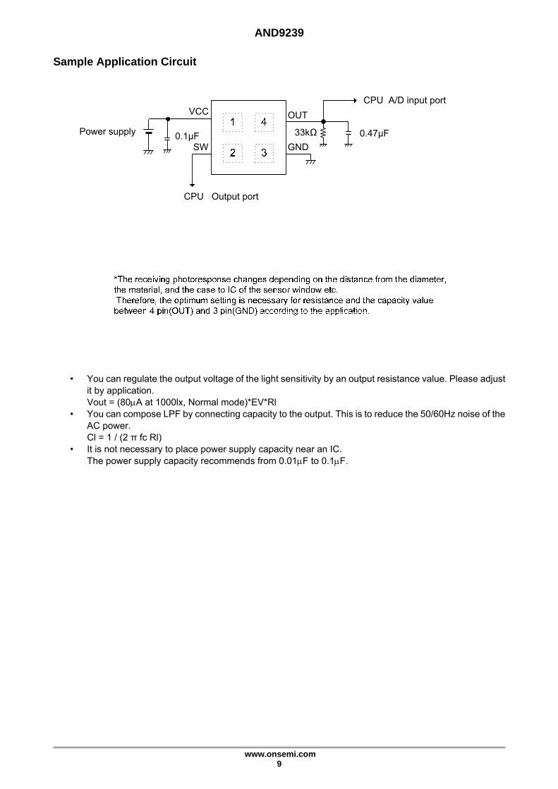
Sample Application Circuit
• You can regulate the output voltage of the light sensitivity by an output resistance value. Please adjust it by application.
Vout = (80A at 1000lx, Normal mode)*EV*Rl • You can compose LPF by connecting capacity to the output. This is to reduce the 50/60Hz noise of the
AC power. Cl = 1 / (2 π fc Rl)
• It is not necessary to place power supply capacity near an IC. The power supply capacity recommends from 0.01F to 0.1F.
Power supply
CPU A/D input port
CPU Output port
VCC
SW
OUT
GND

AND9239
www.onsemi.com 10
Pin Functions
Pin No. Pin Name Pin function Equivalent Circuit
1
VCC Power supply terminal.
Insert a capacitor between this pin and
ground to prevent the influence of noise,
etc.
2 SW Gain change terminal.
This pin is used for gain change.
When this pin is low, "Normal gain".
When this pin is high, "Low gain" .
3 GND Ground terminal.
4 OUT Output terminal.
This pin is outputted the linear current
depending on ambient light.

AND9239
www.onsemi.com 11
Relative Output Current vs Distance • Measuring method
• Evaluation result
• Recommended condition
Hole size φ (optical window) = more than 2mm. Distance from sensor to optical window = less than 2mm.
standard light A
hole sizeΦ
distance S
Illumination Sensor
metal sheet Thickness 0.4mm

AND9239
www.onsemi.com 12
Light Source Dependency
*Fluorescent light is set to “1” Dynamic Current Range
LA0151CS

AND9239
www.onsemi.com 13
Dynamic Voltage Range

AND9239
www.onsemi.com 14
Differential Light Sensibility by PD Location
PD location A is set to “1”
Sensor window
light
2.0
1.8
1.0
0.4 IC
Board (glass epoxy)
Plastic (black : transmission factor=0)
< Side view
Top view
IC
PD
A B C D E
unit mm
A : PD is arranged at the center of the sensor window.
Bto E :The position of PD was rotated.
Sensor window
< >
>
:

AND9239
www.onsemi.com 15
Window design guide Flat window lens design A window lens will surely limit the viewing angle of the LA0151CS. The window lens should be placed directly on top of the LA0151CS. The thickness of the lens should be kept at minimum to minimize loss of power due to reflection and also to minimize loss of loss due to absorption of energy in the plastic material. A thickness of T = 1 mm is recommended for a window lens design. Window with light pipe design If a smaller window is desired while maintaining a wide effective viewing angle of the LA0151CS, a cylindrical piece of transparent plastic is needed to trap the light and then focus and guide the light on to the LA0151CS. Hence the name light guide or also known as light pipe. The pipe should be placed directly on top of the LA0151CS with a distance of Z = 0.5mm to achieve peak performance. The light pipe should have minimum of 1.5mm in diameter to ensure that whole area of the sensor will be exposed.
WD (T+L+Z)
FLAT WINDOW LENS (L=0.0)
WINDOW WITH LIGHT PIPE (D2=1.5, Z=0.5)
Z D1 D1 L 1.5 0.5 2.0 - - 2.0 1.0 3.0 - - 2.5 1.5 4.0 - - 3.0 2 5.0 2.5 1.5
*All dimensions are in mm. *These dimensions are based on a window lens thickness of 1.0mm and a refractive index of 1.59. WD: Distance between window front panel and LA0151CS D1: Window diameter, T: Thickness, L: Length of light pipe D2: Light pipe diameter, Z: Distance between window rear panel and LA0151CS

AND9239
www.onsemi.com 16
Evaluation Board Manual
<Evaluation Board>

AND9239
www.onsemi.com 17
Test Procedure: 1. Connect the test setup as shown above. 2. Connect IC power supply (2.2V to 5.5V) between VCC and GND. 3. Connect multimeter between OUT and GND. 4. Irradiate a light, and put on the illuminance meter near the IC. 5. Control the light source and to be adjusted 500 lux. 6. Then , OUT terminal of LA0151CS is outputted roughly 40A. Therefore, multimeter is showed roughly
1.32V. (1.32V = 40A×33kΩ) LA0151CS features: • No sensibility in infrared area. • Less difference in sensibility depending on the type of light source.
(Please see to page 11 “Light Source Dependency”.) Evaluation Board Circuit Diagram
LA0151CS
VCC
SW
OUT
GND

AND9239
www.onsemi.com 18
Bill of Materials for LA0151CS Evaluation Board
Designator Quantity Description Value Tolerance Footprint ManufacturerManufacturer Part
Number Substitution
Allowed Lead Free
IC1 1 Ambient
Light Sensor - -
ODCSP4 (0.5mm ,pitch)
ON Semiconductor
LA0151CS No yes
R1 1 OUT
(to GND) 33k
(0.063W) ±5%
1005 (0402Inch)
ROHM MCR01MZPJ333 yes yes
C1 1 VCC
Bypass Capacitor
0.1uF /16V
±10% 1005 (0402Inch)
MURATA GRM155B11C104KA yes yes
Evaluation Board PCB Design
( Pattern ) ( Resist ) ( Silk )
(Top View )
IC1
C1R1
Pdmax - Ta
125
25
0
100
200
-30 0 30 60 90 120
Allo
wab
le p
ower
con
sum
ptio
n P
dmax
(m
W)
Specified circuit board6×10×0.5tmm One layer glass epoxy

AND9239
www.onsemi.com 19
Packing Specification of Embossed Carrier Taping ODCSP4 (1.01X1.01)

AND9239
www.onsemi.com 20

AND9239
www.onsemi.com 21

AND9239
www.onsemi.com 22
Lineup of Ambient Light Sensor
Product name LA0151CS LA0152CS LV0111CF LV0104CS
Output type Linear current Linear current Logarithm current 16bitAD digital
Overall size(mm) 1.01×1.01×0.6 1.01×1.01×0.6 1.08×1.08×0.6 1.08×1.08×0.6
Spectral characteristics Normal Normal Closer to visibility Closer to visibility
Gain switching ― ―
Standby function ―
Operating voltage (V) 2.2 to 5.5 2.2 to 5.5 2.3 to 5.5 2.3 to 3.6
Operating temperature range (°C) 30 to 85 30 to 85 30 to 85 30 to 85
Consumption current 1000 lx 150uA 150uA 75uA 70uA
Output current 100 lx 8uA 8uA 20uA 100 counts
Output current 1000 lx 80uA 80uA 30uA 1000 counts
Peak sensitivity (nm) 550 550 550 550
D range 1 to 100k lx 1 to 100k lx 1 to 100k lx 1 to 65k lx
Pb free
Halogen free
Status Mass production Mass production Mass production Mass production
LA0151CS / LA0152CS
0
0.1
0.2
0.3
0.4
0.5
0.6
0.7
0.8
0.9
1
300 400 500 600 700 800 900 1000
Rel
ativ
e se
nsiti
vity
LA0151/52CS Human eye
LV0101CF / LV0104CS
0
0.1
0.2
0.3
0.4
0.5
0.6
0.7
0.8
0.9
1
300 400 500 600 700 800 900 1000
Rel
ativ
e se
nsiti
vity
LV0101CF/04CS Human eye
LA0151CS/LA0152CS LV0111CF/LV0104CS

AND9239
www.onsemi.com 23
ON Semiconductor and the ON logo are registered trademarks of Semiconductor Components Industries, LLC (SCILLC) or its subsidiaries in the United Statesand/or other countries. SCILLC owns the rights to a number of patents, trademarks, copyrights, trade secrets, and other intellectual property. A listing ofSCILLC’s product/patent coverage may be accessed at www.onsemi.com/site/pdf/Patent-Marking.pdf . SCILLC reserves the right to make changes withoutfurther notice to any products herein. SCILLC makes no warranty, representation or guarantee regarding the suitability of its products for any particular purpose,nor does SCILLC assume any liability arising out of the application or use of any product or circuit, and specifically disclaims any and all liability, includingwithout limitation special, consequential or incidental damages. “Typical” parameters which may be provided in SCILLC data sheets and/or specifications canand do vary in different applications and actual performance may vary over time. All operating parameters, including “Typicals” must be validated for eachcustomer application by customer’s technical experts. SCILLC does not convey any license under its patent rights nor the rights of others. SCILLC products arenot designed, intended, or authorized for use as components in systems intended for surgical implant into the body, or other applications intended to support orsustain life, or for any other application in which the failure of the SCILLC product could create a situation where personal injury or death may occur. ShouldBuyer purchase or use SCILLC products for any such unintended or unauthorized application, Buyer shall indemnify and hold SCILLC and its officers,employees, subsidiaries, affiliates, and distributors harmless against all claims, costs, damages, and expenses, and reasonable attorney fees arising out of,directly or indirectly, any claim of personal injury or death associated with such unintended or unauthorized use, even if such claim alleges that SCILLC wasnegligent regarding the design or manufacture of the part. SCILLC is an Equal Opportunity/Affirmative Action Employer. This literature is subject to allapplicable copyright laws and is not for resale in any manner.