Embed Size (px)
Citation preview

1943-0582/12/$31.00©2012IEEE4 WINTER 20 12 IEEE SOLID-STATE CIRCUITS MAGAZINE
Through the Looking Glass
Trend tracking for ISSCC 2012
Kenneth C. Smith, Alice Wang, and Laura C. Fujino
t the IEEE International Solid-State Circuits Conference (ISSCC), there is a long tradition of working to maintain the confer-
ence’s role as the foremost global forum for the presentation of advances in solid-state circuits and systems on a chip (SOCs). But
this implies a great deal of effort on the part of many people. One of the most important elements of this effort is the structuring and organization of the Program Committee, including its subdivision into ten subcommittees focus-ing on diverse technical areas and its dynamic growth and adaptation through the selection of world-renowned specialists. One of the many techniques used by the subcommittees to remain at the forefront of evolving technology is the identifica-tion and maintenance of trend information, on the basis of which new develop-ments become startlingly clear.
The intent of the present article is to share with IEEE Solid-State Circuits Society (SSCS) membership a sampling of the views held by the diverse group of experts rep-resented by the Program Committee, which for ISSCC 2012 is composed of 159 mem-bers. These members are divided into ten subcommittees whose size ranges from 12 to 18 people. This year, the subcommittees are focusing on the following areas: analog; data converters; energy-efficient digital; high-performance digital; imagers, microelectromechanical systems (MEMS), medical, and displays; memory; radio fre-quency; technology directions; wireless; and wireline.
What follows is a sampling of recent analyses and predictions from each of the ten subcomittees.
AnalogAnalog circuits continue to play a key role in modern technology. For example, analog signal amplification is fundamental to interfacing with antennas, microphones, speak-ers, headphones, and image sensors. Analog circuits are bridges between the digital world and the analog real world. Just as with the bridges on our roads, analog circuits often become bottlenecks, and their design is critical to overall performance, effi-ciency, and robustness. Nevertheless, digital circuits such as microprocessors drive the market, and therefore semiconductor technology has been relentlessly optimized over the past 40 years to reduce the size, cost, and power consumption of digital cir-cuits. Analog circuitry, however, has proven increasingly difficult to implement using these modern IC technologies. For example, as the size of transistors has decreased,
Digital Ob ject Id entifier 10.1109/MSSC .2011.2177577
Date of publication: 14 February 2012
A

IEEE SOLID-STATE CIRCUITS MAGAZINE WINTER 20 12 5
the range of analog voltage they can handle has also decreased, and the variation observed in their analog performance has increased.
These aspects of semiconduc-tor technology explain two key divergent trends in analog circuits: One is to forgo the latest digital IC manufacturing technologies, and instead fabricate analog circuits in older technologies, which can be augmented to accommodate the high voltages demanded by medical, automotive, lighting, and industrial applications. Other applications dic-tate a second trend: accepting full integration of analog and digital circuits in the most modern digital semiconductor technology. In such applications, advances in analog interfaces are needed to realize the full potential of digital processing.
For example, mobile systems with multicore digital processors rou-tinely have their battery life lim-ited by the power consumption of traditional analog audio-playback circuits. Modern analog circuits have embedded within them digital signal-processing elements that help overcome analog-circuit limitations; moreover, low-power analog circuits are being embedded within digital ICs to monitor their performance and manage their power consump-tion. Hence, the distinction between analog and digital circuit design is blurring, spawning new advances in the state of the art for both.
The efficient control, storage, and distribution of energy are worldwide challenges and an increasing focus of research in analog circuits. Whereas the manipulation and storage of information is efficiently performed digitally, the manipulation and stor-age of energy must fundamentally be performed using analog systems. As a result, the key technologies for power management are predominantly ana-log. Consequently, there is a great deal
of activity in architectures for dc-dc converters for many applications, such as lighting, multiple-output-voltage generation, and inductorless fully integrated power conversion. There is also an increase in the use of circuits that harvest energy from many sources, such as ambient light, heat, and motion, and then store it and convert it into usable voltages and currents. Currently, much effort is being directed to simultaneously increasing the energy efficiency and power density (power-handling abil-ity per unit of size) of power manage-ment circuits, as shown in Figure 1. Future power management systems will begin to make use of sources with voltages well below 100 mV. At the same time, the power consump-tion of analog circuits is being aggres-sively scaled down in order to enable these low-power systems. Micropower instrumentation amplifiers and oscil-lators and highly efficient audio power amplifiers are two examples of this trend. Together, these technologies will permit devices to be powered indefinitely from sustainable sources,
THE 2012 ISSCC PROGRAM COMMITTEE FRONT ROW, FROM LEFT: DAVID SU, TZI-DAR CHIEUH, BRAM NAUTA, LAURA FUJINO, HIDETO HIDAKA, HOI-JUN YOO, AND KEVIN ZHANG. BACK ROW, FROM LEFT: ROLAND THEWES, BILL REDMAN-WHITE, AARNO PARSSINEN, ANANTHA CHANDRAKSAN, VENU GOPINATHAN, ANDREIA CATHELIN, STEFAN RUSU, DAVID FRIEDMAN, MAKOTO IKEDA. NOT PICTURED IS SUBCOMMITTEE CHAIR SIVA NARENDRA.

6 WINTER 20 12 IEEE SOLID-STATE CIRCUITS MAGAZINE
opening the door to ubiquitous sens-ing, environmental monitoring, and diverse medical applications.
Data ConvertersThe march of progress in converter designs involves exploiting the inherent trade-offs between signal-to-noise ratio (SNR), bandwidth, sampling frequency, and power effi-ciency, especially when all need to be improved. This year, at ISSCC 2012,
new and improved design combina-tions are being presented.
Figure 2 shows power efficiency in terms of power dissipation per Hertz at the Nyquist frequency ver-sus signal-to-noise-and-distortion ratio (SNDR). Since higher SNDR requires more power, constant figure-of-merit (FoM) trend lines in the plot are proportional to SNDR. The small dots in the graph are previously published ISSCC results,
while the ISSCC 2012 contributions are indicated by the large trian-gles, squares, and circles. As the plot indicates, ISSCC 2012 data con-verters have once again extended the state-of-the-art.
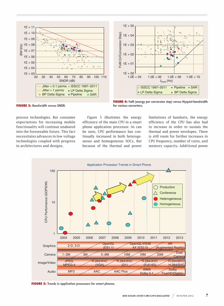
Figure 3 shows bandwidth versus SNDR. Generally speaking, band-width is lower at higher SNDR, as is indicated in the figure. The trend lines correspond to two values of clock jitter, 0.1 and 1 ps root mean square (psrms). In this figure, it can be seen that bandpass delta-sigma converters are especially pushing the state of the art.
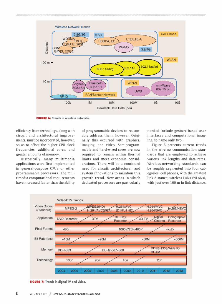
Figure 4 shows the FoM versus Nyquist-bandwidth. At low frequen-cies, the FoM is optimal (low FoM is better), but as the graph shows, the FoM is deteriorating at higher fre-quencies. This is primarily caused by the speed limitation of pres-ently available technology. As can be noted, designs presented at ISSCC 2012 show good progress, with a successive-approximation regis-ter (SAR) pushing the state of the art at lower frequencies and a pipeline design breaking the barrier at higher frequencies.
Energy-Efficient DigitalThe energy efficiency of digital cir-cuits becomes increasingly impor-tant as larger and larger numbers of transistors are integrated on a single chip. This is particularly important for mobile applications in multime-dia and communications.
Multimedia and communication technologies have enhanced the lives of mobile consumers by increasing productivity, enhancing the social networking experience, and deliv-ering improved visual and audio quality for communication links and entertainment. In this develop-ment, the performance of embedded CPUs has increased to meet the rising demands of general-purpose compu-tations. At the same time, dedicated multimedia accelerators provide a solution for well-defined, energy-effi-cient signal processing constrained by the physical limitations of advanced
95.0
90.0
85.0
80.0
75.0
70.0
65.0
60.0
55.0
50.00.1 1 10
Power Density (mW/mm2)
CMOS
90 nm
Trench Capacitors2
3
5
SOI + 32 nm
32 nm
Efficiency <-> Power Density
100 1,000 10,000
Pea
k E
ffici
ency
(%
)
ISSCC’12
FIGURE 1: Trends in integrated power conversion. Each year, more and more is integrated in standard CMOS technologies, optimizing efficiency versus power density. At ISSCC 2012, these trends are evident in a shift to higher performance, as shown by the arrow.
20 30 40 50 60
SNDR (dB)
1E – 01
1E + 00
1E + 01
1E + 02P/f s
nyq
(pJ)
1E + 03
1E + 04
1E + 05
1E + 06
70 80 90 100 110
LP Delta SigmaBP Delta Sigma SARPipeline
FoM = 10 f/Conversion StepFoM = 100 f/Conversion Step ISSCC 1997–2011
FIGURE 2: Power efficiency versus SNR, highlighting ISSCC 2012 results.
IEEE SOLID-STATE CIRCUITS MAGAZINE WINTER 20 12 7
process technologies. But consumer expectations for increasing mobile functionality will continue unabated into the foreseeable future. This fact necessitates advances in low-voltage technologies coupled with progress in architectures and designs.
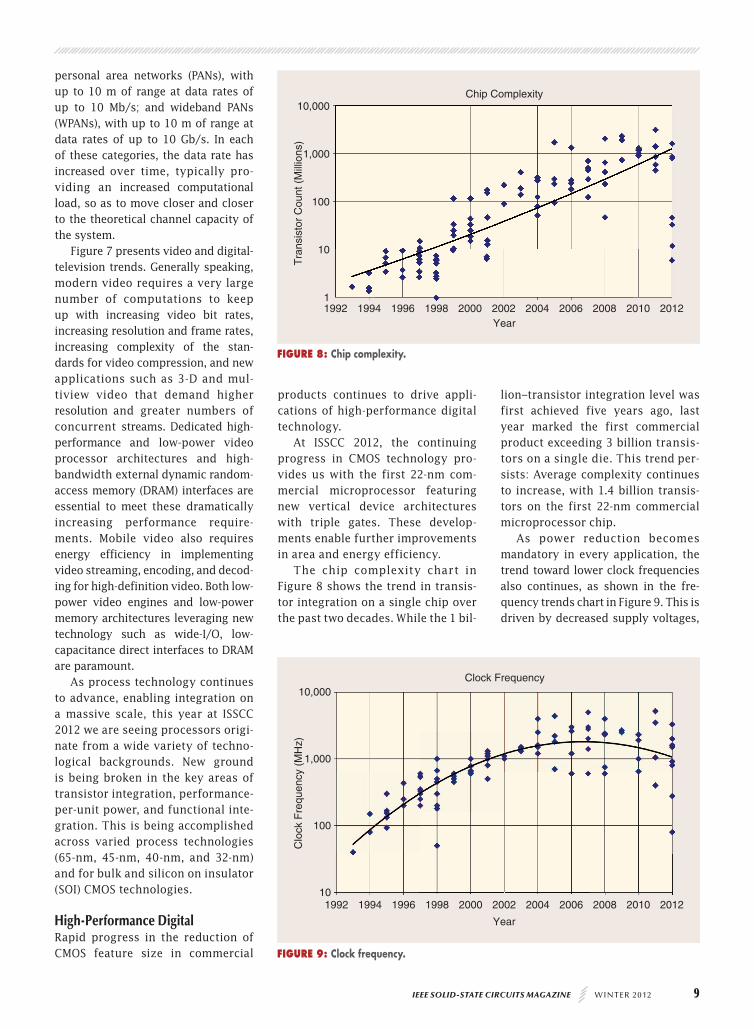
Figure 5 illustrates the energy efficiency of the main CPU in a smart phone application processor. As can be seen, CPU performance has con-tinually increased in both heteroge-neous and homogeneous SOCs. But because of the thermal and power
limitations of handsets, the energy efficiency of the CPU has also had to increase in order to sustain the thermal and power envelopes. There is still room for further increases in CPU frequency, number of cores, and memory capacity. Additional power
20 30 40 50SNDR (dB)
1E + 03
BW
(H
z)
1E + 04
1E + 05
1E + 06
1E + 07
1E + 08
1E + 09
1E + 10
1E + 11
60 70 80 90 100 110
LP Delta SigmaBP Delta Sigma Pipeline SARJitter = 1 psrmsJitter = 0.1 psrms ISSCC 1997–2011
FIGURE 3: Bandwidth versus SNDR.
1.0E + 04 1.0E + 06 1.0E + 08fsnyq (Hz)
FoM
(fJ
/Con
vers
ion
Ste
p)
1.0E + 101E + 00
1E + 01
1E + 02
1E + 03
1E + 04
1E + 05
BP Delta SigmaLP Delta Sigma
SARPipelineISSCC 1997–2011
FIGURE 4: FoM (energy per conversion step) versus Nyquist-bandwidth for various converters.
12004
Graphics 2-D, 3-D
1~2M
JPEG,MPEG-4
MP3 AAC AAC PlusWMA
Dolby 5.1Dolby
TrueHD/Digital+
H.264/AVC(VGA)
H.264/AVC(D1)
H.264/AVC(Full HD)
H.264/MVCH.264/SVC
3M 5~8M 10M 16M 20MDual
Camera
OpenGL(ES1.1)
OpenGL/VG/MAX (ES2.0)
AR(Augmented Reality)
Camera
Image/Video
Audio
2005 2006 2007 2008 2009 2010 2011 2012 2013
Application Processor Trends in Smart Phone
10
100
CP
U P
erfo
rman
ce (
GO
PS
/W)
Production
Conference
Heterogeneous
Homogeneous
FIGURE 5: Trends in application processors for smart phones.
8 WINTER 20 12 IEEE SOLID-STATE CIRCUITS MAGAZINE
efficiency from technology, along with circuit and architectural improve-ments, must be incorporated, however, so as to offset the higher CPU clock frequencies, additional cores, and greater amounts of memory.
Historically, many multimedia applications were first implemented in general-purpose CPUs or other programmable processors. The mul-timedia computational requirements have increased faster than the ability
of programmable devices to reason-ably address them, however. Origi-nally this occurred with graphics, imaging, and video. Semiprogram-mable and hard-wired cores are now required to remain within thermal limits and meet economic consid-erations. There will be a continued need for circuit, architectural, and system innovations to maintain this growth trend. New areas in which dedicated processors are particularly
needed include gesture-based user interfaces and computational imag-ing, to name only two.
Figure 6 presents current trends in the wireless-communication stan-dards that are employed to achieve various link lengths and data rates. Wireless-networking standards can be roughly segmented into four cat-egories: cell phones, with the greatest link distance; wireless LANs (WLANs), with just over 100 m in link distance;
100k
RF-IDPAN/Sensor Network
Zigbee802.15.4
GSMGPRS, EDGE
CDMA1x, 2000
WCDMAUMTS
2.5G/3G
Wireless Network Trends
3.5G
3.9/4G
HSDPA, Etc.LTE/LTE-A
WiMAX
802.11a/b/g 802.11n 802.11ac/ad
Bluetooth802.15.1
WPAN
WLAN
Cell Phone
UWB
mm-Wave802.15.3c
10 m
100 m
Dis
tanc
e
1M 10M
Downlink Data Rate (b/s)
100M 1G 10G
FIGURE 6: Trends in wireless networks.
MPEG-2
DVD Recorder
480i
~10M
DDR-333
130n
2004
Technology
Memory
Bit Rate (b/s)
Pixel Format
Application
Video Codec(Standard)
Video/DTV Trends
2005 2006 2007 2008 2009 2010 2011 2012 2013
90n 45n 28n
DDR2-667~800DDR3-1333/Wide IODRAM
~20M ~50M ~300M
1080i/720P/480P 4kx2k
DTVBlu-RayRecorder
3D TVDigitalCinema
HolographicRecorder
MPEG2(HD)H.264/AVC(VGA)
H.264/AVC(D1/Full HD)
H.264/MVCH.264/SVC
H.265/HEVC
FIGURE 7: Trends in digital TV and video.
IEEE SOLID-STATE CIRCUITS MAGAZINE WINTER 20 12 9
personal area networks (PANs), with up to 10 m of range at data rates of up to 10 Mb/s; and wideband PANs (WPANs), with up to 10 m of range at data rates of up to 10 Gb/s. In each of these categories, the data rate has increased over time, typically pro-viding an increased computational load, so as to move closer and closer to the theoretical channel capacity of the system.
Figure 7 presents video and digital-television trends. Generally speaking, modern video requires a very large number of computations to keep up with increasing video bit rates, increasing resolution and frame rates, increasing complexity of the stan-dards for video compression, and new applications such as 3-D and mul-tiview video that demand higher resolution and greater numbers of concurrent streams. Dedicated high-performance and low-power video processor architectures and high-bandwidth external dynamic random-access memory (DRAM) interfaces are essential to meet these dramatically increasing performance require-ments. Mobile video also requires energy efficiency in implementing video streaming, encoding, and decod-ing for high-definition video. Both low-power video engines and low-power memory architectures leveraging new technology such as wide-I/O, low-capacitance direct interfaces to DRAM are paramount.
As process technology continues to advance, enabling integration on a massive scale, this year at ISSCC 2012 we are seeing processors origi-nate from a wide variety of techno-logical backgrounds. New ground is being broken in the key areas of transistor integration, performance-per-unit power, and functional inte-gration. This is being accomplished across varied process technologies (65-nm, 45-nm, 40-nm, and 32-nm) and for bulk and silicon on insulator (SOI) CMOS technologies.
High-Performance DigitalRapid progress in the reduction of CMOS feature size in commercial
products continues to drive appli-cations of high-performance digital technology.
At ISSCC 2012, the continuing progress in CMOS technology pro-vides us with the first 22-nm com-mercial microprocessor featuring new vertical device architectures with triple gates. These develop-ments enable further improvements in area and energy efficiency.
The chip complexity chart in Figure 8 shows the trend in transis-tor integration on a single chip over the past two decades. While the 1 bil-
lion–transistor integration level was first achieved five years ago, last year marked the first commercial product exceeding 3 billion transis-tors on a single die. This trend per-sists: Average complexity continues to increase, with 1.4 billion transis-tors on the first 22-nm commercial microprocessor chip.
As power reduction becomes mandatory in every application, the trend toward lower clock frequencies also continues, as shown in the fre-quency trends chart in Figure 9. This is driven by decreased supply voltages,
199210
100
1,000
10,000
Clo
ck F
requ
ency
(M
Hz)
1994 1996 1998 2000 2002 2004 2006 2008 2010 2012
Year
Clock Frequency
FIGURE 9: Clock frequency.
1992 1994 1996 1998 2000 2002 2004 2006 2008 2010 2012Year
Tra
nsis
tor
Cou
nt (
Mill
ions
)
Chip Complexity
1
10
100
1,000
10,000
FIGURE 8: Chip complexity.

10 WINTER 20 12 IEEE SOLID-STATE CIRCUITS MAGAZINE
with processors operating in the near-threshold or even the subthreshold voltage domain. The performance loss resulting from reduced volt-ages and clock frequencies is com-pensated for by further increased parallelism. Leveraging sophisti-cated strategies to lower leakage and manage voltage, variability, and aging has bolstered the continuing reduc-tion in total power dissipation. This is helping to rein in the immense power demands from PCs, servers, and simi-lar systems. Consequently, it yields solutions with less cost and reduced cooling requirements, resulting in greener products.
In addition to the trend toward integrating more cores on a single chip, shown in the core trend chart in Figure 10, additional dedicated coprocessing units for graphics and communications are now commonly integrated on these complex SOCs. It is worth noting that the design of such SOCs requires broad collaboration across multiple disciplines, includ-ing circuits, architecture, graphics, process technology, system design, energy efficiency, and software.
High-performance and power-effi-cient computing techniques continue to be introduced for targeted critical applications, such as floating-point
and single-instruction, multiple-data (SIMD) processors. As a result, we can see a downward trend in power consumption, as shown in the power trend chart in Figure 11.
ISSCC 2012 marks the wider introduction of massively parallel, 3-D-integrated systems. In such sys-tems, a third dimension of integra-tion becomes available by stacking monolithically integrated dies and interconnecting them by applying innovative TSV technologies. The result of this integration is a new level of performance in a power-efficient package.
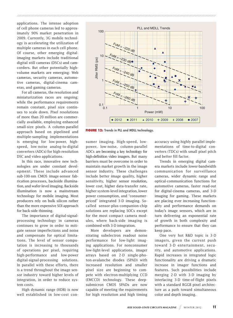
Another trend evident this year is the continued emergence of all-dig-ital phase-locked loops (PLLs) and delay-locked loops (DLLs) to better exploit deep-submicron-feature-size scaling, thereby reducing power and area costs. Due to the application of highly innovative architectural and circuit-design techniques, the fea-tures of these all-digital PLLs and DLLs have improved significantly over the past several years. The rms-jitter-versus-power diagram in Figure 12 shows the improvement of the widely accepted FoM for PLLs and multiplying delay-locked loops (MDLLs).
Clearly, the rapid downward re -duction of feature size continues to force the replacement of tradition-ally analog techniques.
Imagers, MEMS, Medical, and Displays (IMMD)The common thread that unites the constituents of IMMD is a con-cern for interfaces with the physical world—both the human body and its environment. Conventionally, we consider this broad area in terms of both task and tool: imagers, MEMS, medical, and displays, as discussed in the following subsections.
ImagersThe CMOS image sensor business remains one of the fastest-growing seg-ments of the semiconductor industry, due to the proliferation of cell phone cameras and other digital-imaging
0
Cor
e C
ount
10
20
30
40
50
60
70
2000 2001 2002 2003
Year
Core Count
2004 2005 2006 2007 2008 2009 2010 2011 2012
FIGURE 10: Core count.
19920
Total Power Consumption
50Pow
er C
onsu
mpt
ion
(W)
100
150
200
250
1994 1996 1998 2000 2002 2004 2006 2008 2010 2012
Year
FIGURE 11: Total power consumption.
IEEE SOLID-STATE CIRCUITS MAGAZINE WINTER 20 12 11
applications. The intense adoption of cell phone cameras led to approx-imately 90% market penetration in 2009. Currently, 3G mobile technol-ogy is accelerating the utilization of multiple cameras in each cell phone. Of course, other emerging digital-imaging markets include traditional digital still cameras (DSCs) and cam-corders. But other potentially high-volume markets are emerging: Web cameras, security cameras, automo-tive cameras, digital-cinema cam-eras, and gaming cameras.
For all cameras, the resolution and miniaturization races are ongoing; while the performance requirements remain constant, pixel size contin-ues to scale down. Pixel resolutions of more than 20 million are commer-cially available, employing enhanced small-size pixels. A column-parallel approach based on pipelined and multiple-sampling implementations is emerging for low-power, high-speed, low-noise analog-to-digital converters (ADCs) for high-resolution DSC and video applications.
In this race, innovative new tech-nologies are under constant devel-opment. These include advanced sub-100-nm CMOS image-sensor fab-rication processes, backside illumina-tion, and wafer-level imaging. Backside illumination is now a mainstream technology for mobile imaging. Most producers rely on bulk silicon rather than the more expensive SOI approach for back-side thinning.
The importance of digital-signal-processing technology in cameras continues to grow in order to miti-gate sensor imperfections and noise and compensate for optical limita-tions. The level of sensor compu-tation is increasing to thousands of operations per pixel, requiring high-performance and low-power digital-signal-processing solutions. In parallel with these efforts, there is a trend throughout the image sen-sor industry toward higher levels of integration, in order to reduce sys-tem costs.
High dynamic range (HDR) is now well established in low-cost con-
sumer imaging. High-speed, low-power, low-noise, column-parallel ADCs are becoming a key technology for high-definition video imagers. But many barriers must be overcome in order to maintain market growth in the image sensor industry. These challenges include better image quality, higher sensitivity, higher sensor resolution, lower cost, higher data-transfer rate, higher system-level integration, lower power consumption, and “consumer-priced” integrated 3-D imaging. So-called sensor-plus-companion-chip solutions are replacing SOCs except for the most compact camera mod-ules, where back-side imaging is combined with 3-D integration.
More developers are demon-strating subelectron readout noise performance for low-light imag-ing applications. For nonconsumer low-light-level applications, imager arrays based on 2-D single-pho-ton-avalanche diodes (SPAD) with increased resolution and smaller pixel size are beginning to com-pete with electron-multiplying CCD (EMCCD) technology. These deep-submicron CMOS SPADs are now capable of meeting the requirements for high resolution and high timing
accuracy using highly parallel imple-mentations of time-to-digital con-verters (TDCs) with small pixel pitch and better fill factor.
Trends in emerging digital cam-era markets include lower-bandwidth communication for surveillance cameras, wider dynamic range and optical-communication functions for automotive cameras, faster read-out for digital-cinema cameras, and 3-D imaging for gaming. These markets are placing ever increasing function-ality and performance demands on today’s image sensors, which are in turn delivering an exponential rate of growth in both complexity and performance to ensure that they can keep pace.
One very hot R&D topic is 3-D imagers, given the current push toward 3-D entertainment, secu-rity, and automotive applications. Rapid increases in integrated logic functionality are driving a dramatic increase in imager functions and features. Such possibilities include merging 2-D with 3-D imaging by interlacing 3-D time-of-flight pixels with a standard RGGB pixel architec-ture as a path toward simultaneous color and depth imaging.
0.10.1
FoM = –260 dB
FoM = –250 dB
FoM = –240 dB
FoM = –230 dB
FoM = –220 dB
Jitte
r R
MS
(ps
)
1
10
100
1Power (mW)
PLL and MDLL Trends
2012 2011 2010 2009 2008 2007
10 100
FIGURE 12: Trends in PLL and MDLL technology.

12 WINTER 20 12 IEEE SOLID-STATE CIRCUITS MAGAZINE
The market share for CCDs con-tinues to shrink in machine vision, compact DSC, and security applica-tions. Only within top-end broad-cast and top-end digital cameras do CCDs still maintain a significant market share.
Sensors and MEMS CMOS temperature sensors continue to improve, reaching higher temper-atures (200 8C), with finer resolution (100µ 8C/!Hz), in shorter conver-sion times (10 µs), with simpler cali-bration (using voltage rather than temperature), and using smaller die sizes (0.006 mm2).
New technologies for tempera-ture sensors are maturing; in partic-ular, thermal diffusivity is proving to be a valuable sensing phenomenon, reaching both high temperatures and good accuracy. Small-area, high-speed temperature sensors in highly scaled 22-nm CMOS technology will be important for microprocessors so as to limit die temperatures to safe values.
MEMS oscillators are improving. Phase noise is now low enough for demanding RF applications; 12-kHz–20-MHz jitter is now below 1 ps; and frequency accuracy is now better than 0.5 ppm. MEMS microphones, accelerometers, and pressure sen-sors continue to improve as they become common in consumer and automotive applications.
BiomedicalThere is an increasing interest in neural applications, with significant R&D activity in the field of biopo-tential sensors for neural record-ing and stimulation. Such activity includes the following trends:
■ Closed-loop systems are being commercialized: a closed-loop, ac-celeration-sensor-enabled neuro-stimulation device is CE-marked in Europe, and a closed-loop epi-lepsy device has completed clini-cal trials. The latter is a major in-novation that leverages the latest sensor and circuit technology for neural interfacing, allowing for
novel diagnostics based on chron-ic recording.
■ Brain-machine interface systems are now transferring into pilot clinical trials, although there con-tinues to be some debate about “best methods.” While acute hu-man testing shows that only a low degree of freedom is needed to control robotic arms in paralyzed patients, methods are being ex-tended for a broader range of neu-ral applications.
■ Continuing efforts are enabling high-spatial-resolution, multichan-nel neural stimulators (such as those for retinal stimulation) and stimulators with recorders (such as those used in brain research). For example, a retinal implant with 60 pixels has received a CE mark, a step forward in the design of a sophisticated prosthesis. Work to increase complexity by another or-der of magnitude is ongoing.
The demand for telemedicine, remote sensing, and economical design is expanding as the population ages and cost pressures increase. These pressures are growing significantly with health care reform; the eco-nomic value of technical solutions is now being considered along with safety and efficacy.
Silicon technology is enabling new paradigms for biological signal processing. Examples include:
■ Along with 32-bit processing cores, 0.13-µm foundry-based CMOS technology is stabilizing as a low-power process for biomedical pur-poses. The partitioning of signal processing between the analog and digital domains is still being debat-ed, with both modalities reaching levels that allow for chronic moni-toring with minimal energy drain.
■ Silicon-based arrays are emerging for analyzing genomes and im-munoassays. Multiple paradigms are being explored to eliminate the need for expensive optical com-ponents. It is being proposed not only to perform hybridization as-says on-chip but to allow direct DNA sequencing as well.
90
Intel Cell
45, 0.346
65, 0.57
90, 190, 1
65, 1
40, 0.9
28, 1 20, 0.95
40, 1.1
65, 1.290, 1.2
28, 0.85 20, 0.85
40, 0.242
65, 0.525
20, 0.081
32, 0.171
22, 0.092
TSMC Cell VDD_LP
65 45
Technology Node (nm)
0
Bit
Cel
l Siz
e (µ
m2 )
VD
D_L
P, V
DD
_G (
V)
0.2
0.4
0.6
0.8
1
1.2
0
0.2
0.4
0.6
0.8
1
1.2
1.41.4Bit Cell Trend
40 32 28 22 20
28, 0.127
90, 0.999
FIGURE 13: Trends for SRAM bit cells.
IEEE SOLID-STATE CIRCUITS MAGAZINE WINTER 20 12 13
DisplaysSingle-chip sensing and driving for touch-integrated liquid-crystal display (LCD) panels is one of the display-technology trends for much thinner and lower-cost realizations. Advanced 3-D LCD TV technologies are opening up a new era of 3-D home theater. The current focus is on how to make more realistic views that are comfortable to the eye. Technolo-gies for 3-D realization that do not require glasses and their driving electronics are emerging for mobile and notebook applications.
MemoryDevelopment of mainstream memory technologies continues unabated. The major thrust concerns embed-ded memories, i.e., static random-access memory (SRAM), DRAM, and floating-gate-based flash, for very broad applications. As processes con-tinue to shrink in an effort to follow Moore’s law, however, each incum-bent technology is encountering difficulty in maintaining the trend line. Cells in SRAM, DRAM, and flash are becoming ever more difficult to scale. In response to the challenges, we see logic processes adopting trigate/ 3-D devices, along with assist circuits for SRAM read and write. Meanwhile, certain emerging mem-ory technologies are making rapid progress toward product intro-duction, including phase-change RAM (PCRAM) and magnetoresistive RAM (MRAM), while resistance RAM (ReRAM or RRAM) is gaining ground for future applications.
Current state-of-the-art results from ISSCC 2012 include:
■ the first SRAM using FinFETs op-erating at 4.6 GHz using trigate devices with assist circuits for lower VCCmin
■ a density-record-beating 19-nm, 128-Gb TLC NAND flash memory
■ a new DDR4 3.2-Gb/s/pin, 4-Gb, 30-nm SDRAM with PVT-tolerant data fetch
■ a high-speed 443-MB/s–write–throughput, multilayered, cross-point ReRAM macro.
SRAMEmbedded SRAM continues to be an important element in a wide range of very large scale integra-tion (VLSI) applications, from high-performance processors to handheld devices. Historically, the SRAM bit cell has followed Moore’s law, shrinking in area by about 50% with each new generation, as shown in Figure 13. This reduction has enabled designers to put more SRAM bits on each die, improving performance. Another key perfor-mance metric for SRAM design is the
lowest reliable operating voltage. A low value lets memory blocks oper-ate reliably with the same (or better) power envelope, as compared with the previous generation. As the tran-sistor feature size marches below 20 nm, device variation has made it very difficult to shrink the bit-cell area at the 50% rate while main-taining or lowering VCCmin
between generations. Starting at 45 nm, the introduction of high-K metal gates has reduced the Vt mismatch and enabled further device scaling by significantly reducing the equivalent
1
2000 2002 2004 2006
Year
Sto
rage
Cap
acity
(M
b)
2008 2010 2012
10
100
1,000
10,000
100,000Condition 1 MbISSCC, VLSI Circuits, ASSCCIEDM, VLSI Technology
128 Gb
NAND Flash
8 Gb
PRAM
FeRAM 128 Mb
64 Mb
MRAMRRAM
64 Mb
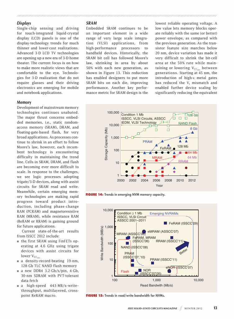
FIGURE 14: Trends in emerging NVM memory capacity.
1100 1,000
Read Bandwith (Mb/s)
Flash(ISSCC’07’05)
10,000
Writ
e B
andw
idth
(M
B/s
)
10
100
1,000
10,000
NOReNOR (ISSCC’07)
PRAM (ISSCC’11)(ISSCC’07,’10)
Better
PRAM
NAND (ISSCC’08)
RRAM (ISSCC’11)(ISSCC’06)FeRAM, MRAM
eMRAM (ASSCC’07)
FeRAM (ISSCC’09)
MRAM (ASSCC’06)
Condition ≥ 1 Mb Emerging NVRAMs
ASSCC 2001–2011ISSCC, VLSl Circuit
FIGURE 15: Trends in read/write bandwidth for NVMs.
14 WINTER 20 12 IEEE SOLID-STATE CIRCUITS MAGAZINE
oxide thickness. Design solutions such as read/write assist circuitry have been used to improve the VCCmin
performance at the memory-macro level for 32 nm and beyond. New transistor structures such as Fin-FET and FD-SOI are emerging as the replacement for planar devices to
enable further area reduction and VCCmin
scaling of SRAM bit cells.
Nonvolatile MemoriesIn recent years, technological and chip development for emerging non-volatile memories (NVMs) has been intensified, using advanced materi-
als. The emerging NVMs, such as PCRAM, ferroelectric RAM (FeRAM), MRAM, and ReRAM, all have excel-lent read/write and endurance per-formance, as well as low power requirements as compared with flash memory. These new NVMs offer the potential to open up new mar-kets and applications. Commercial uses have been very slow to appear because of the rapid reduction of per-bit costs of conventional flash memory technologies already on the market, as shown in Figure 14. But the new technologies seem set to capture some specific markets by taking advantage of merits such as high read/write bandwidth (in the hundreds of megabytes per second), as shown in Figure 15. This year, ISSCC 2012 will report on a num-ber of high-density 20-nm and sub-20-nm designs.
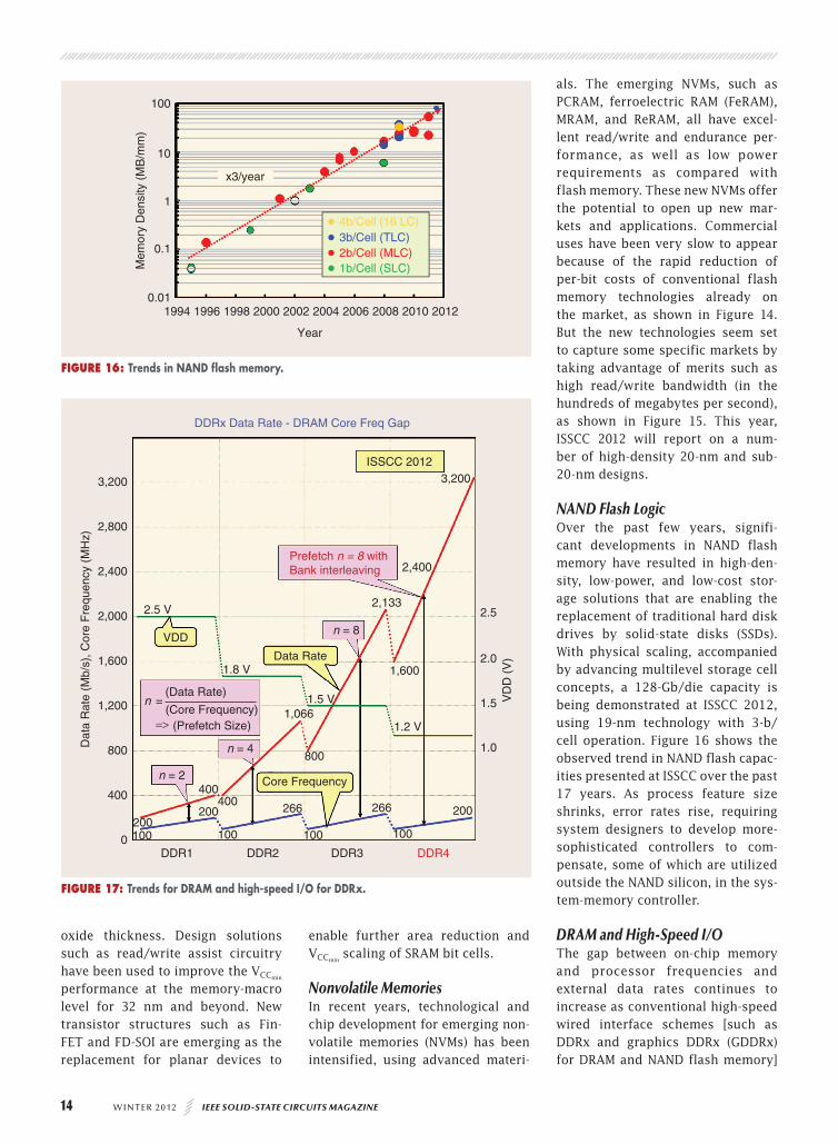
NAND Flash LogicOver the past few years, signifi-cant developments in NAND flash memory have resulted in high-den-sity, low-power, and low-cost stor-age solutions that are enabling the replacement of traditional hard disk drives by solid-state disks (SSDs). With physical scaling, accompanied by advancing multilevel storage cell concepts, a 128-Gb/die capacity is being demonstrated at ISSCC 2012, using 19-nm technology with 3-b/cell operation. Figure 16 shows the observed trend in NAND flash capac-ities presented at ISSCC over the past 17 years. As process feature size shrinks, error rates rise, requiring system designers to develop more-sophisticated controllers to com-pensate, some of which are utilized outside the NAND silicon, in the sys-tem-memory controller.
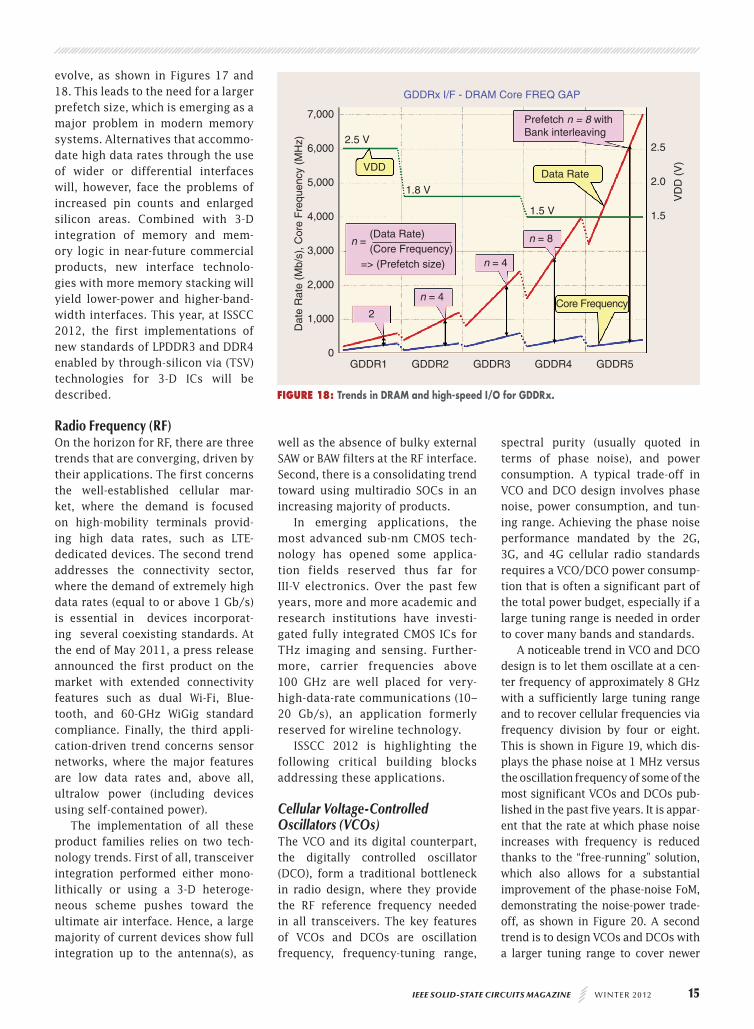
DRAM and High-Speed I/OThe gap between on-chip memory and processor frequencies and external data rates continues to increase as conventional high-speed wired interface schemes [such as DDRx and graphics DDRx (GDDRx) for DRAM and NAND flash memory]
1994 1996 1998 2000 2002 2004 2006 2008 2010 2012
Year
4b/Cell (16 LC)3b/Cell (TLC)2b/Cell (MLC)1b/Cell (SLC)
0.01
0.1
1
10
100
Mem
ory
Den
sity
(M
B/m
m)
x3/year
FIGURE 16: Trends in NAND flash memory.
DDR1
DDRx Data Rate - DRAM Core Freq Gap
0 100 100 100 100
200
800
1.2 V
1.5 V
1.8 V
2.5 V
Prefetch n = 8 withBank interleaving
2,133
2,400
1,066
1,600
266 266
3,200ISSCC 2012
Core Frequency
(Data Rate)
(Core Frequency)(Prefetch Size)
=
=>
Data Rate
VDD
200200
400
n = 2
n = 4
n = 8
n
400
Dat
a R
ate
(Mb/
s), C
ore
Fre
quen
cy (
MH
z)
400
800 1.0
1.5 VD
D (
V)2.0
2.5
1,200
1,600
2,000
2,400
2,800
3,200
DDR2 DDR3 DDR4
FIGURE 17: Trends for DRAM and high-speed I/O for DDRx.
IEEE SOLID-STATE CIRCUITS MAGAZINE WINTER 20 12 15
evolve, as shown in Figures 17 and 18. This leads to the need for a larger prefetch size, which is emerging as a major problem in modern memory systems. Alternatives that accommo-date high data rates through the use of wider or differential interfaces will, however, face the problems of increased pin counts and enlarged silicon areas. Combined with 3-D integration of memory and mem-ory logic in near-future commercial products, new interface technolo-gies with more memory stacking will yield lower-power and higher-band-width interfaces. This year, at ISSCC 2012, the first implementations of new standards of LPDDR3 and DDR4 enabled by through-silicon via (TSV) technologies for 3-D ICs will be described.
Radio Frequency (RF)On the horizon for RF, there are three trends that are converging, driven by their applications. The first concerns the well-established cellular mar-ket, where the demand is focused on high-mobility terminals provid-ing high data rates, such as LTE-dedicated devices. The second trend addresses the connectivity sector, where the demand of extremely high data rates (equal to or above 1 Gb/s) is essential in devices incorporat-ing several coexisting standards. At the end of May 2011, a press release announced the first product on the market with extended connectivity features such as dual Wi-Fi, Blue-tooth, and 60-GHz WiGig standard compliance. Finally, the third appli-cation-driven trend concerns sensor networks, where the major features are low data rates and, above all, ultralow power (including devices using self-contained power).
The implementation of all these product families relies on two tech-nology trends. First of all, transceiver integration performed either mono-lithically or using a 3-D heteroge-neous scheme pushes toward the ultimate air interface. Hence, a large majority of current devices show full integration up to the antenna(s), as
well as the absence of bulky external SAW or BAW filters at the RF interface. Second, there is a consolidating trend toward using multiradio SOCs in an increasing majority of products.
In emerging applications, the most advanced sub-nm CMOS tech-nology has opened some applica-tion fields reserved thus far for III-V electronics. Over the past few years, more and more academic and research institutions have investi-gated fully integrated CMOS ICs for THz imaging and sensing. Further-more, carrier frequencies above 100 GHz are well placed for very-high-data-rate communications (10–20 Gb/s), an application formerly reserved for wireline technology.
ISSCC 2012 is highlighting the following critical building blocks addressing these applications.
Cellular Voltage-Controlled Oscillators (VCOs)The VCO and its digital counterpart, the digitally controlled oscillator (DCO), form a traditional bottleneck in radio design, where they provide the RF reference frequency needed in all transceivers. The key features of VCOs and DCOs are oscillation frequency, frequency-tuning range,
spectral purity (usually quoted in terms of phase noise), and power consumption. A typical trade-off in VCO and DCO design involves phase noise, power consumption, and tun-ing range. Achieving the phase noise performance mandated by the 2G, 3G, and 4G cellular radio standards requires a VCO/DCO power consump-tion that is often a significant part of the total power budget, especially if a large tuning range is needed in order to cover many bands and standards.
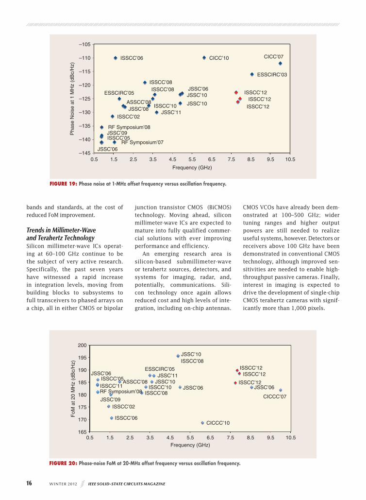
A noticeable trend in VCO and DCO design is to let them oscillate at a cen-ter frequency of approximately 8 GHz with a sufficiently large tuning range and to recover cellular frequencies via frequency division by four or eight. This is shown in Figure 19, which dis-plays the phase noise at 1 MHz versus the oscillation frequency of some of the most significant VCOs and DCOs pub-lished in the past five years. It is appar-ent that the rate at which phase noise increases with frequency is reduced thanks to the “free-running” solution, which also allows for a substantial improvement of the phase-noise FoM, demonstrating the noise-power trade-off, as shown in Figure 20. A second trend is to design VCOs and DCOs with a larger tuning range to cover newer
GDDR10
1.5
2.0
2.5
VD
D (
V)
Dat
e R
ate
(Mb/
s), C
ore
Fre
quen
cy (
MH
z)
1,000
2,000
3,000
4,000
5,000
6,000
7,000
2
(Data Rate)
Prefetch n = 8 withBank interleaving
GDDRx I/F - DRAM Core FREQ GAP
(Core Frequency)=> (Prefetch size)
VDD
2.5 V
1.8 V
1.5 V
Core Frequency
Data Rate
n = 4
n = 4
n = 8n =
GDDR2 GDDR3 GDDR4 GDDR5
FIGURE 18: Trends in DRAM and high-speed I/O for GDDRx.
16 WINTER 20 12 IEEE SOLID-STATE CIRCUITS MAGAZINE
bands and standards, at the cost of reduced FoM improvement.
Trends in Millimeter-Wave and Terahertz TechnologySilicon millimeter-wave ICs operat-ing at 60–100 GHz continue to be the subject of very active research. Specifically, the past seven years have witnessed a rapid increase in integration levels, moving from building blocks to subsystems to full transceivers to phased arrays on a chip, all in either CMOS or bipolar
junction transistor CMOS (BiCMOS) technology. Moving ahead, silicon millimeter-wave ICs are expected to mature into fully qualified commer-cial solutions with ever improving performance and efficiency.
An emerging research area is silicon-based submillimeter-wave or terahertz sources, detectors, and systems for imaging, radar, and, potentially, communications. Sili-con technology once again allows reduced cost and high levels of inte-gration, including on-chip antennas.
CMOS VCOs have already been dem-onstrated at 100–500 GHz; wider tuning ranges and higher output powers are still needed to realize useful systems, however. Detectors or receivers above 100 GHz have been demonstrated in conventional CMOS technology, although improved sen-sitivities are needed to enable high-throughput passive cameras. Finally, interest in imaging is expected to drive the development of single-chip CMOS terahertz cameras with signif-icantly more than 1,000 pixels.
0.5165
170
175
180
185
190
200
195
ISSCC’06
ISSCC’02
ISSCC’11ISSCC’05
ASSCC’08
ISSCC’08
ISSCC’12
ISSCC’12ISSCC’12
ESSCIRC’05
JSSC’09
JSSC’06
JSSC’10
JSSC’06
JSSC’11
JSSC’06
CICCC’10
CICCC’07
JSSC’10ISSCC’10
ISSCC’08RF Symposium’08
1.5 2.5 3.5 4.5 5.5 6.5 7.5 8.5 9.5 10.5Frequency (GHz)
FoM
at 2
0 M
Hz
(dB
c/H
z)
FIGURE 20: Phase-noise FoM at 20-MHz offset frequency versus oscillation frequency.
0.5–145
–140
–135
–130
–125
–120
–115
–110
–105
1.5 2.5
JSSC’06
JSSC’09
RF Symposium’07
RF Symposium’08
ISSCC’02
ISSCC’10
ISSCC’12
ISSCC’06
ISSCC’12ISSCC’12
ESSCIRC’03
CICC’10 CICC’07
ISSCC’08ISSCC’08
JSSC’11
JSSC’06JSSC’10
JSSC’10JSSC’08
ASSCC’08
ESSCIRC’05
ISSCC’05
3.5 4.5 5.5 6.5 7.5 8.5 9.5 10.5
Frequency (GHz)
Pha
se N
oise
at 1
MH
z (d
Bc/
Hz)
FIGURE 19: Phase noise at 1-MHz offset frequency versus oscillation frequency.
IEEE SOLID-STATE CIRCUITS MAGAZINE WINTER 20 12 17
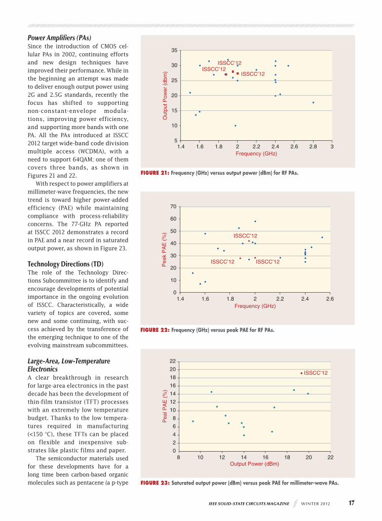
Power Amplifiers (PAs)Since the introduction of CMOS cel-lular PAs in 2002, continuing efforts and new design techniques have improved their performance. While in the beginning an attempt was made to deliver enough output power using 2G and 2.5G standards, recently the focus has shifted to supporting non-constant-envelope modula-tions, improving power efficiency, and supporting more bands with one PA. All the PAs introduced at ISSCC 2012 target wide-band code division multiple access (WCDMA), with a need to support 64QAM; one of them covers three bands, as shown in Figures 21 and 22.
With respect to power amplifiers at millimeter-wave frequencies, the new trend is toward higher power-added efficiency (PAE) while maintaining compliance with process-reliability concerns. The 77-GHz PA reported at ISSCC 2012 demonstrates a record in PAE and a near record in saturated output power, as shown in Figure 23.
Technology Directions (TD)The role of the Technology Direc-tions Subcommittee is to identify and encourage developments of potential importance in the ongoing evolution of ISSCC. Characteristically, a wide variety of topics are covered, some new and some continuing, with suc-cess achieved by the transference of the emerging technique to one of the evolving mainstream subcommittees.
Large-Area, Low-Temperature ElectronicsA clear breakthrough in research for large-area electronics in the past decade has been the development of thin-film transistor (TFT) processes with an extremely low temperature budget. Thanks to the low tempera-tures required in manufacturing (<150 8C), these TFTs can be placed on flexible and inexpensive sub-strates like plastic films and paper.
The semiconductor materials used for these developments have for a long time been carbon-based organic molecules such as pentacene (a p-type
1.45
10
15
20
25
30
35
1.6 1.8 2 2.2 2.4 2.6 2.8 3Frequency (GHz)
ISSCC’12ISSCC’12
ISSCC’12
Out
put P
ower
(db
m)
FIGURE 21: Frequency (GHz) versus output power (dBm) for RF PAs.
1.40
10
20
30
40
50
60
70
1.6 1.8 2 2.2 2.4 2.6Frequency (GHz)
ISSCC’12 ISSCC’12
ISSCC’12
Pea
k P
AE
(%
)
FIGURE 22: Frequency (GHz) versus peak PAE for RF PAs.
80
2
4
6
8
10
12
14
16
18
20
22
10 12 14 16 18 20 22Output Power (dBm)
ISSCC’12
Pea
l PA
E (
%)
FIGURE 23: Saturated output power (dBm) versus peak PAE for millimeter-wave PAs.

18 WINTER 20 12 IEEE SOLID-STATE CIRCUITS MAGAZINE
semiconductor). More recently, organic n-type semiconductors and amor-phous metal oxides, which are also n-type semiconductors, have emerged. Popular metal-oxide semiconductors are zinc oxide (ZnO) and amorphous indium–gallium–zinc oxide (IGZO or GIZO). The mobility of n- and p-type organic materials has reached val-ues around 1 cm2/Vs, while metal oxides have surpassed the 10-cm2/Vs
mark. The operational stability of all semiconductor materials has greatly improved and should be sufficient to enable commercial applications, espe-cially in combination with the large-area compatible barrier layers used to seal the transistor stack.
At the current state of the art, p-type-only, n-type-only, and comple-mentary technologies are available. Most TFTs are still manufactured with subtractive methods based on lithog-raphy, but there is a clear emphasis on the development of additive tech-nologies that could provide higher production throughput. These are based on various technologies bor-rowed from the graphic printing world, such as gravure, screen print-ing, and offset.
The technology road map in the field of large-area and low-tem-perature electronics thus focuses on lowering the cost per unit area instead of increasing the number of functions per unit area, which is the focus of monocrystalline Si technol-ogy according to Moore’s law.
Traditional applications such as flexible displays and electronic RFID tags integrated in the wrapping of retail goods, together with the improve-ment of TFT performance, reliability, and aging stability, have enabled first prototypes of applications integrat-ing sensors and actuators with low-
temperature TFTs. Examples include signage, pressure- and light-sensi-tive foils, sheets capable of distrib-uting RF power to appliances, and energy-scavenging devices.
Following this trend, ISSCC 2012 features a flexible pedometer pow-ered by foot motion, a flexible touch pad based on organic TFTs, an RFID capable of bidirectional commu-nication using organic and metal-oxide TFTs, and an IGZO DAC that can be used as an integrated column driver in OLED display backplanes, as shown in Figures 24 and 25.
WirelessData rates for modern wireless standards are increasing rapidly. This is evident from cellular stan-dard trends, as shown in Figure 26. In fact, the data rate has increased by a factor of 100 over the past decade, and another increase by a factor of ten is projected over the next five years. This trend has been maintained by using more com-plex modulation techniques such as orthogonal-frequency-division multiplexing (OFDM) for better spec-tral efficiency but has come at the cost of increased requirements for digital signal processing (DSP). In addition, the expansion of channel bandwidth is also an effective way to achieve a data-rate increase. This can be seen in the wireless-connec-tivity trend chart (for 802.113) in Figure 27. It is clear from the fig-ure that channel bandwidth for the WLAN standards has increased from the traditional 20 MHz (802.11g) to 40 MHz (802.11n), then to 160 MHz (802.11ac), and finally to .1 GHz (802.11ad). Because the available spectrum is limited in the low-GHz range, to achieve .1-GHz channel bandwidth, the carrier frequency has been moved from 2.4/5 GHz (802.11a/b/g/n) to 60 GHz (802.11ad) in the millimeter-wave range.
With the spectrum available in the 60-GHz range, data rates greater than 1 Gb/s can be achieved with modest modulation. The initial feasibility of 60-GHz CMOS was demonstrated in
2-V OrganicPMOS Circuits
Piezoelectric Energy Harvester(PVDF Sheet)
22 cm
FIGURE 24: A flexible insole pedometer: a device that counts steps while being powered by the movement of the foot itself, made with an organic piezoelectric foil (PVDF) coupled to an organic p-type circuit. (Used with permission from ISSCC.)
FIGURE 25: A touch pad using a capacitive sensor employing organic p-type transistors. (Used with permission from ISSCC.)

IEEE SOLID-STATE CIRCUITS MAGAZINE WINTER 20 12 19
2009. Then a Silicon Valley start-up, SiBeam, demonstrated a complete end-to-end system that supports a robust wireless link in 60 GHz and achieves 3.8 Gb/s in 1.76 GHz. This demonstration ignited more research and development from both academia and industry in millimeter-wave communication.
An old problem sees a new solu-tion. As wireless applications pro-liferate, the spectrum is becoming very crowded because of the many licensed and unlicensed uses occu-pying most of the assigned fre-quency bands. But cognitive radio is an answer: it promises to identify and utilize spectral “white space” in the presence of many other wireless applications. And so the current trend for cognitive radio is to design highly linear transceivers that can cover a very wide frequency range, with various channel bandwidths. As a consequence of these high-linearity wide-band design require-ments, distortion-cancellation and tunable-RF channel-selection tech-niques are critical. Most transceiv-ers in this category are adopting digital calibration and analog feed-back techniques to increase the linearity performance for a very tunable front end so as to cover a wide range of frequencies.
On another front, wireless sensor networks (WSNs) require ultralow-power radio to increase the life-time of the battery—or better still, to eliminate the battery completely using energy harvesting. To reduce the power consumption of the radio, the first approach is to use the radio only when it is requested. Wake-up radio thus becomes one of the main building blocks of each WSN node. Once the radio awakens, power effi-ciency becomes the main target for both high- and low-data-rate com-munication. Such WSNs will enable electronics for sustainability.
WirelineWireline continues to be an impor-tant application of semiconductor technology as the need for wired
communication flows out from its long distance origins into smaller and smaller environments, through backplanes to inter- and intrachip connection. A continuing challenge in this evolution is the adaptation of techniques that originated on a large scale to shrinking environments.
High-speed I/O bandwidth needs are increasing by about a factor of two each year as the requirements for data transmission gather momen-tum, driven by the use of the cloud and data streaming. Along with the increase in data rates, such systems are also rapidly approaching power limits that constrain the I/O band-
widths. There is also a need for backward compatibility across the legacy-interconnect chassis that adds to the development challenge.
Wireline interconnects using serial links—once a niche application in high-speed network routers—are now used in a wide range of applications, from high-speed microprocessors to data converters. To meet integration requirements, these serial links must have lower power, even as performance increases. Hence, a typical FoM consid-ers the energy required per transmit/receive bit or pJ/bit, which is the ratio of the power in milliwatts to the data rate in gigabits per second, or mW/Gb/s.
Wirelss Data Rate: Connectivity
802.11
1E + 10
1E + 9
1E + 8
1E + 7
1E + 61995
b/s
2000 2005 2010 2015
802.11g802.11ac MIMO
802.11b 802.11a802.11n MIMO802.11n SISO
802.11ad - 60 GHz+
FIGURE 27: Trends in the data rates of wireless-connectivity standards (802.11x).
Wireless Data Rate: Cellular
1G-AMPS-DL 1G-AMPS-UL 2G-GSM-DL3G-WCDMA-DL4G-LTE-DL
2G-GSM-UL3G-WCDMA-UL4G-LTE-UL
2G-CDMA-DL 2G-CDMA-UL3G-EVDO-DL
1E + 9
1E + 8
1E + 7
1E + 6
1E + 5
1E + 4
1E + 31980 1985 1990 1995 2000 2005 2010 2015
b/s
3G-EVDO-UL
FIGURE 26: Trends in cellular-standards data rates.

20 WINTER 20 12 IEEE SOLID-STATE CIRCUITS MAGAZINE
The past five years have seen serial-link speeds increasing from 1 Gb/s, but a barrier appears to be approaching fast. Although limited, specialized 40 Gb/s links have been developed for telecom applications, and ini-tial 40 Gb/s links have been demonstrated in the lab; links able to support a broad set of applications at rates above 40 Gb/s or able to support 50 Gb/s rates at all are conspicu-ously absent commercially.
Therefore, although the system challenges require data bandwidth to increase by a fac-tor of about two each year, existing technology only allows data rates to increase by a factor of two every five years. At the same time, the need to support a variety of data channels, including legacy compatibility, with a very large number of parallel links means that equalization techniques are essential for robust data trans-mission. Receiver equalization meth-ods include the “linear” type, for boosting the signals for shorter and less complex channels, and “decision feedback,” for more complex chan-nels with interchannel crosstalk. These equalization techniques add to the power consumed by the links, however.
Figure 28 shows the energy effi-ciency per bit of equalizing receiv-ers reported since 2007. The state of the art is around 0.5 pJ/b for equalizers operating at less than 20 Gb/s. At higher data rates, how-ever, the energy efficiency is still greater than 1 pJ/b. This year, ISSCC 2012 is presenting best-in-class performance in terms of data rate at 16 Gb/s with energy efficiency of less than 0.5 pJ/b, showing the extension of low-power equalizers to higher data rates.
For a combined transmitter and receiver channel, the mW/Gb/s FoM depends on the target applica-tion. Today, for short-reach serial
links where the equalization is not as complex, achievable power num-bers are of the order of 1–5 mW/Gb/s; state-of-the-art 10-Gb/s links typically consume between 10 and 50 mW. For higher data rates (in the range of 25–30 Gb/s), the efficiency is typically lower because of the additional clock and analog perfor-mance requirements imposed by the high data rate. The state of the art at these data rates is therefore in the range of 8–10 mW/Gb/s.
Long-reach links and more complex channels such as cop-per backplanes that include mul-tiple connectors have much higher power consumption and lower effi-ciency in terms of mW/Gb/s. This year, ISSCC 2012 is presenting the first 28-Gb/s transceiver to address medium-reach applications using 32-nm SOI and consuming 693 mW for 35 db of channel loss with an FoM of 24.75 mW/Gb/s.
These trends in integration, power consumption, and appli-cations bring new challenges to wireline communications. New tech-niques are required to ensure con-tinued downscaling of the links, and improvements in equalization tech-niques, transmitter design, receiver design, and clock distribution are essential. ISSCC 2012 will highlight many of the new techniques that continue to enhance the field.
SummaryDevelopments reported at ISSCC 2012 continue to pres-ent breakthroughs in the broad domain of solid-state circuits and systems. In this rich environment, presenta-tions at ISSCC characteristi-cally predict ways in which electronics techniques will fulfill the present and future needs of society. In this role, ISSCC continues to present a road map of things to come, both in the immediate future and in the longer term.
AcknowledgmentsThe authors wish to acknowledge the creators of the original material from which this article has been struc-tured. While this has been largely a team effort by several members of each subcommittee, each has oper-ated under the direction of his or her subcommittee chair, as listed below:
■ Analog: Bill Redman-White, NXP Semiconductors
■ Data Converters: Venu Gopina-than, Texas Instruments
■ Energy-Efficient Digital: Tzi-Dar Chiueh, National Chip Implemen-tation Center
■ High-Performance Digital: Stefan Rusu, Intel
■ Imagers, MEMS, Medical, and Dis-plays: Roland Thewes, TU Berlin
■ Memory: Kevin Zhang, Intel ■ Radio Frequency: Andreia Cathe-
lin, STMicroelectronics ■ Technology Directions: Siva Nar-
endra, Tyfone ■ Wireless: David Su, Atheros Com-
munications ■ Wireline: Daniel Friedman, IBM Thom-
as J. Watson Research Center.
About the Authors Kenneth C. Smith is with the Uni-versity of Toronto in Canada.
Alice Wang is with Texas Instru-ments in Dallas, Texas.
Laura C. Fujino is with the Uni-versity of Toronto in Canada.
FIGURE 28: Power efficiency of equalizing receivers. The star represents the low-power equalizer operating at 16 GB/s and consuming <0.5 pJ/b, as reported at ISSCC 2012.
2.5
2
1.5
1
0.5
05 10 15
Data RateP
ower
Effi
cien
cy (
pJ/b
)20 25
90 nm CMOS65 nm CMOS45 nm CMOS32 nm CMOS
90 nm CMOS65 nm CMOS45 nm CMOS32 nm CMOS
64 Mb


![[Marketing trend] 2015 Marketing Trend](https://img.dokumen.tips/doc/110x75/55a896cc1a28ab193e8b4598/marketing-trend-2015-marketing-trend.jpg)