Embed Size (px)
Citation preview
Analysis and Design of Robust Storage Elements
in Nanometric Circuits
A Dissertation Presented
by
Sheng Lin
to
The Department of Electrical and Computer Engineering
in partial fulfillment of the requirements
for the degree of
Doctor of Philosophy
in
Computer Engineering
Northeastern University
Boston, Massachusetts
May 2011

NORTHEASTERN UNIVERSITYGraduate School of Engineering
Dissertation Title: Analysis and Design of Robust Storage Elements in Nanometric
Circuits.
Author: Sheng Lin.
Department: Electrical and Computer Engineering.
Approved for Dissertation Requirements of the Doctor of Philosophy Degree
Dissertation Co-Advisor: Prof. Fabrizio Lombardi Date
Dissertation Co-Advisor: Prof. Yong-Bin Kim Date
Dissertation Reader: Prof. Gunar Schirner Date
Department Chair: Prof. Ali Abur Date
Director of the Graduate School:
Dean: Prof. Sara Wadia-Fascetti Date
Abstract
The stability of storage element circuits in the nanoscale era, such as memories and
latches is evaluated and new circuit configurations for stability improvement are pro-
posed in this dissertation. The stability and robustness of a given memory cell are
usually evaluated by analyzing both static and dynamic behaviors during typical op-
eration. In this dissertation, a 9T CMOS SRAM cell design at 32nm is first presented
to improve static stability, power dissipation, and delay compared to the conventional
SRAM cell as well as a detailed comparison with other designs found in the technical
literature. Moreover, a dual-diameter Carbon Nanotube-based SRAM cell configu-
ration with different threshold voltages is then designed; this cell shows significant
improvements compared to its CMOS counterpart in terms of power consumption
and stability.
Two memory cell configurations at 32nm CMOS technology for improving dy-
namic stability are then proposed in this dissertation and simulation results show
significant improvement in dynamic stability. In this work, a comprehensive treat-
ment (model, analysis and design) for hardening storage elements against a soft error
resulting in multiple node upsets is also presented. A novel 13T memory cell configu-
ration is proposed and simulated to show a significantly better tolerance to the likely
multiple node upset. Simulation results have confirmed that the proposed memory
cell accomplish an excellent soft error tolerance through hardening and an impressive
power-delay product compared with the other commonly used hardened design.
For the latch, the stability of a latch cell is only judged by the Critical Charge
(Qcrit) when the latch is not transparent. Three new hardened designs for CMOS
latches at 32nm feature size are proposed. For the latch design, a novel design metric
ii

iii
(QPAR) is introduced to assess the overall design effectiveness such as area, perfor-
mance, power, and soft error tolerance. It has been shown in the dissertation that
the proposed latch achieved the best overall performance compared with the existing
designs. The multiple node upset analysis is also extended to hardened latches; it is
shown that the latch with the highest critical charge has also the best tolerance to
multiple node upsets.
Acknowledgements
It is a pleasure to thank many people who made this dissertation possible.
I would like to express my gratitude to my advisors, Dr. Fabrizio Lombardi and
Dr. Yong-Bin Kim, whose expertise, understanding, and patience, added considerably
to my graduate experience. I appreciate their vast knowledge in many areas, and their
assistance in writing technical articles. Throughout my thesis-writing period, they
provided encouragement, sound advice, good teaching, and lots of good ideas.
I am especially grateful to the member of my dissertation committee, Dr. Schirner,
and the faculty members of the Department of Electrical and Computer Engineering
Department for the help and training that enabled me to my work on this disserta-
tion. Their valuable suggestions were really helpful and enhanced the conceptual and
methodological clarity of my research work.
Many thank, to many student colleagues of mine for providing a collaborative, stim-
ulating and enjoyable environment. It has been a great pleasure to work in the
Computer Engineering Lab of the Northeastern University.
I am grateful to all the staff members at the ECE department, the College of Engi-
neering and NU ISSI for all their kind assistance over the years.
Finally, I want to dedicate this work to my parents. Words can not express my
gratitude to them, Xiangyu Lin and Yuling Wu, for their support and love, which I
owe all my achievements to. Without them, none of these could have accomplished.
Boston, Massachusetts Sheng Lin
May 2, 2011
iv
Table of Contents
Table of Contents iv
List of Tables vii
List of Figures viii
1 Introduction 1
1.1 Overview . . . . . . . . . . . . . . . . . . . . . . . . . . . . . . . . . . 1
1.1.1 Design Issues of robust SRAM cells . . . . . . . . . . . . . . . 5
1.1.2 Design Issues of robust latches . . . . . . . . . . . . . . . . . . 9
1.2 Previous Work . . . . . . . . . . . . . . . . . . . . . . . . . . . . . . 11
1.3 Dissertation Outline . . . . . . . . . . . . . . . . . . . . . . . . . . . 13
2 Analysis and Design of CMOS SRAM Cell for Low Leakage and
High Stability 17
2.1 Introduction . . . . . . . . . . . . . . . . . . . . . . . . . . . . . . . . 17
2.2 Review of SRAM Cells . . . . . . . . . . . . . . . . . . . . . . . . . . 19
2.2.1 Conventional 6T Cell . . . . . . . . . . . . . . . . . . . . . . . 19
2.2.2 8T and 10T Cell . . . . . . . . . . . . . . . . . . . . . . . . . 19
2.3 Proposed 9T SRAM Cell . . . . . . . . . . . . . . . . . . . . . . . . . 22
2.3.1 9T Cell Scheme . . . . . . . . . . . . . . . . . . . . . . . . . . 22
2.3.2 Data Stability and Write-ability . . . . . . . . . . . . . . . . . 27
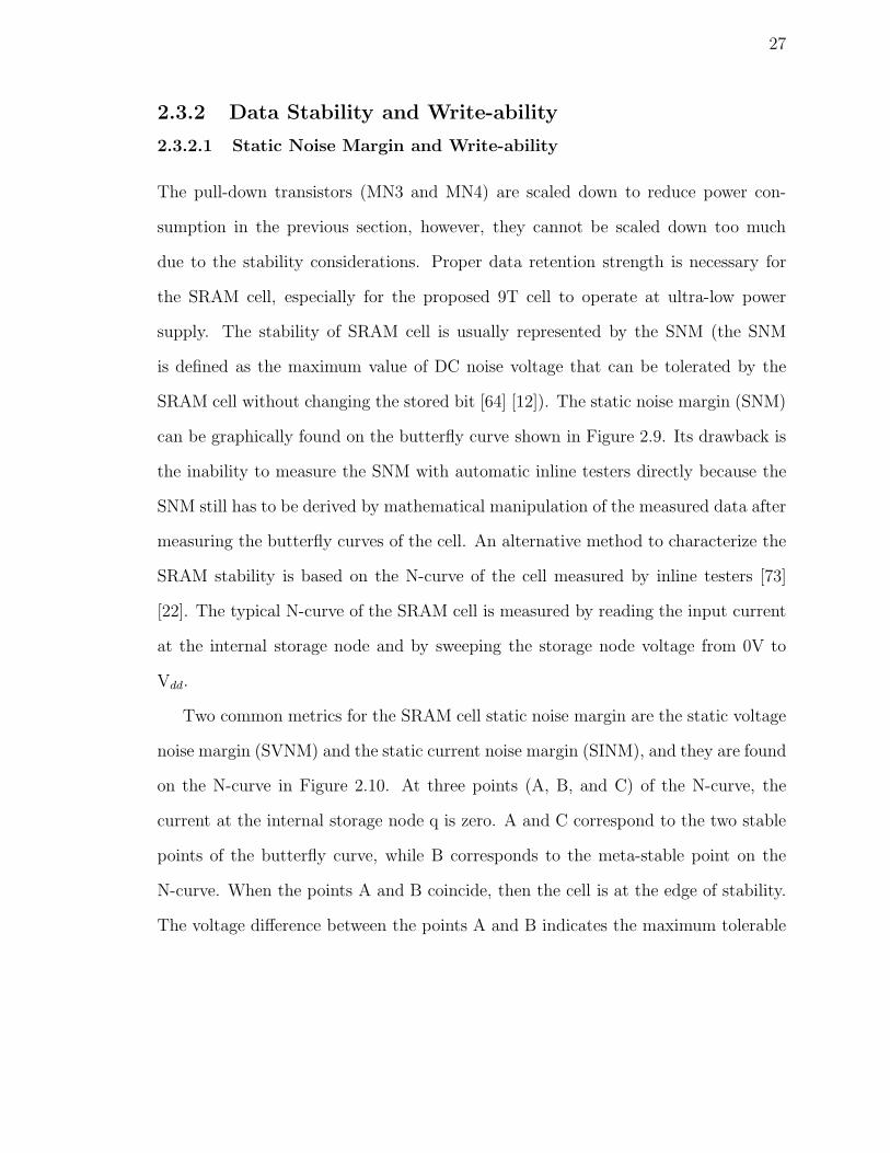
2.3.2.1 Static Noise Margin and Write-ability . . . . . . . . 27
2.3.2.2 Soft Errors and Dynamic Stability . . . . . . . . . . 30
2.3.2.3 Area . . . . . . . . . . . . . . . . . . . . . . . . . . . 32
2.3.2.4 Standby Power Reduction . . . . . . . . . . . . . . . 34
2.4 A Metric for Memory Cells . . . . . . . . . . . . . . . . . . . . . . . . 37
2.5 Impact of PVT Variations . . . . . . . . . . . . . . . . . . . . . . . . 40
2.6 Conclusion . . . . . . . . . . . . . . . . . . . . . . . . . . . . . . . . . 44
iv
3 Analysis and Design of CNTFET SRAM Cell for Low Leakage and
High Stability 48
3.1 Introduction . . . . . . . . . . . . . . . . . . . . . . . . . . . . . . . . 48
3.2 Carborn Nanotube Field Effect Transister . . . . . . . . . . . . . . . 50
3.3 Design of 6T SRAM using CNTFET . . . . . . . . . . . . . . . . . . 55
3.3.1 Read Operation . . . . . . . . . . . . . . . . . . . . . . . . . . 56
3.3.2 Write Operation . . . . . . . . . . . . . . . . . . . . . . . . . 58
3.4 Dual-Chirality SRAM Cell Design . . . . . . . . . . . . . . . . . . . . 60
3.5 A Metric for Memory Cells . . . . . . . . . . . . . . . . . . . . . . . . 64
3.6 Impact of Parameter Variations . . . . . . . . . . . . . . . . . . . . . 66
3.7 Conclusion . . . . . . . . . . . . . . . . . . . . . . . . . . . . . . . . . 68
4 Analysis and Design of Soft Error Hardened Memory 70
4.1 Introduction . . . . . . . . . . . . . . . . . . . . . . . . . . . . . . . . 70
4.2 Soft Error Modeling for SRAM Cell . . . . . . . . . . . . . . . . . . . 73
4.3 Proposed 14T Hardened Memory Design . . . . . . . . . . . . . . . . 74
4.3.1 Existing Hardening Approach in First Category . . . . . . . . 74
4.3.2 Proposed 14T Hardened Memory Cell . . . . . . . . . . . . . . 76
4.3.3 Transistor Sizing Optimization . . . . . . . . . . . . . . . . . . 78
4.3.4 Impact of Variations on 14T Hardened Cell . . . . . . . . . . 84
4.4 Existing Hardened Memory Design in Second Category . . . . . . . . 87
4.4.1 DICE Cell . . . . . . . . . . . . . . . . . . . . . . . . . . . . . 87
4.4.2 Hardened Cell Proposed in [47] . . . . . . . . . . . . . . . . . 87
4.5 Proposed 11T Hardened Memory Design . . . . . . . . . . . . . . . . 91
4.6 Evaluation of the Proposed 11T Hardened Cell . . . . . . . . . . . . . 94
4.6.1 Critical Charge . . . . . . . . . . . . . . . . . . . . . . . . . . 95
4.6.2 Area, Power and Delay . . . . . . . . . . . . . . . . . . . . . . 96
4.6.3 Impact of Process Variation . . . . . . . . . . . . . . . . . . . 99
4.7 Multiple Node Upset Analysis on Hardened Memory Cells . . . . . . 100
4.7.1 Multiple Node Upset Modeling . . . . . . . . . . . . . . . . . 101
4.8 Proposed 13T Hardened Memory Design . . . . . . . . . . . . . . . . 103
4.9 Evaluation of the 13T Memory Cell . . . . . . . . . . . . . . . . . . . 104
4.9.1 Multiple Node Upset Tolerance . . . . . . . . . . . . . . . . . 105
4.9.2 Area, Power and Delay . . . . . . . . . . . . . . . . . . . . . . 107
4.9.3 Parameter Variations . . . . . . . . . . . . . . . . . . . . . . . 109
4.10 Conclusion . . . . . . . . . . . . . . . . . . . . . . . . . . . . . . . . . 111
v

5 Analysis and Design of Soft Error Hardened Latches 114
5.1 Introduction . . . . . . . . . . . . . . . . . . . . . . . . . . . . . . . . 114
5.2 Soft Error Modeling . . . . . . . . . . . . . . . . . . . . . . . . . . . 115
5.3 Conventional Latch . . . . . . . . . . . . . . . . . . . . . . . . . . . . 116
5.4 Existing Hardened Latches . . . . . . . . . . . . . . . . . . . . . . . . 117
5.5 Proposed Hardened Latches . . . . . . . . . . . . . . . . . . . . . . . 120
5.5.1 Modified SEM-latch . . . . . . . . . . . . . . . . . . . . . . . 120
5.5.2 Alternative Schmitt Trigger Latch . . . . . . . . . . . . . . . . 121
5.5.3 Cascode Schmitt Trigger Latch . . . . . . . . . . . . . . . . . 122
5.6 Assessment and Comparison of Hardened Latches . . . . . . . . . . . 124
5.6.1 Timing and Delay . . . . . . . . . . . . . . . . . . . . . . . . . 124
5.6.2 Area . . . . . . . . . . . . . . . . . . . . . . . . . . . . . . . . 125
5.6.3 Critical Charge . . . . . . . . . . . . . . . . . . . . . . . . . . 126
5.6.4 Power-delay Product and Critical Charge . . . . . . . . . . . . 131
5.6.5 Process Variations . . . . . . . . . . . . . . . . . . . . . . . . 132
5.7 Multiple Node Upset Analysis . . . . . . . . . . . . . . . . . . . . . . 133
5.7.1 Multiple Node Upset Tolerance . . . . . . . . . . . . . . . . . 134
5.7.2 Process Variation Impact on Multiple Node Upset Tolerance . 135
5.8 Conclusion . . . . . . . . . . . . . . . . . . . . . . . . . . . . . . . . . 137
6 Summary and Future Works 139
6.1 Summary of Contributions . . . . . . . . . . . . . . . . . . . . . . . . 139
6.2 Future Works . . . . . . . . . . . . . . . . . . . . . . . . . . . . . . . 142
6.2.1 Single Event Upset Tolerant Latch Design . . . . . . . . . . . 142
6.2.2 CNTFET-based Hardened Design . . . . . . . . . . . . . . . . 143
Bibliography 144
vi
List of Tables
2.1 Noise margin comparison at 0.9V Power Supply, Slow Corner, and 100◦
C Temperature . . . . . . . . . . . . . . . . . . . . . . . . . . . . . . 29
2.2 Power dissipation comparison at 0.6V Power Supply and Room Tem-
perature . . . . . . . . . . . . . . . . . . . . . . . . . . . . . . . . . . 38
3.1 SNM and Write Time of the SRAM Cells at 0.9V Power Supply and
Room Temperature . . . . . . . . . . . . . . . . . . . . . . . . . . . . 63
3.2 SPR of SRAM Cells at 0.9V Power Supply and Room Temperature . 66
4.1 Critical charge, SNM, and Performance comparison of Different Mem-
ory cells at 0.9V Power Supply and Room Temperature . . . . . . . . 82
4.2 Process Variation Impact on SRAM Cell Stability . . . . . . . . . . . 86
4.3 Geometric Parameter of Memory Cells . . . . . . . . . . . . . . . . . 97
4.4 Failure probability of memory cells with PVT variations . . . . . . . 111
5.1 Critical Charge, Performance, Power Comparison Between Hardened
Latches at 0.9V Power Supply and Room Temperature . . . . . . . . 126
5.2 Area of Latches . . . . . . . . . . . . . . . . . . . . . . . . . . . . . . 126
5.3 QPAR of Latches . . . . . . . . . . . . . . . . . . . . . . . . . . . . . 130
5.4 Critical Charges and Failure Probability of Latches . . . . . . . . . . 134
5.5 Failure probability of latches with PVT variations . . . . . . . . . . . 137
vii

List of Figures
1.1 Unrolled graphite sheet . . . . . . . . . . . . . . . . . . . . . . . . . . 4
1.2 Cross section view of a CNTFET . . . . . . . . . . . . . . . . . . . . 5
1.3 Conventional 6T memory cell . . . . . . . . . . . . . . . . . . . . . . 5
1.4 Voltage transfer characteristics of a CMOS inverter . . . . . . . . . . 7
1.5 Static Noise Margin (SNM) of a 6T SRAM cell . . . . . . . . . . . . 7
1.6 Conventional latch cell . . . . . . . . . . . . . . . . . . . . . . . . . . 9
2.1 Conventional 6T SRAM cell and its worst-case stability condition . . 20
2.2 Hold and read butterfly plot of the conventional 6T SRAM cell at
power supply voltage of 0.6V . . . . . . . . . . . . . . . . . . . . . . . 20
2.3 8T SRAM cell . . . . . . . . . . . . . . . . . . . . . . . . . . . . . . . 21
2.4 10T SRAM cell in [8] . . . . . . . . . . . . . . . . . . . . . . . . . . . 21
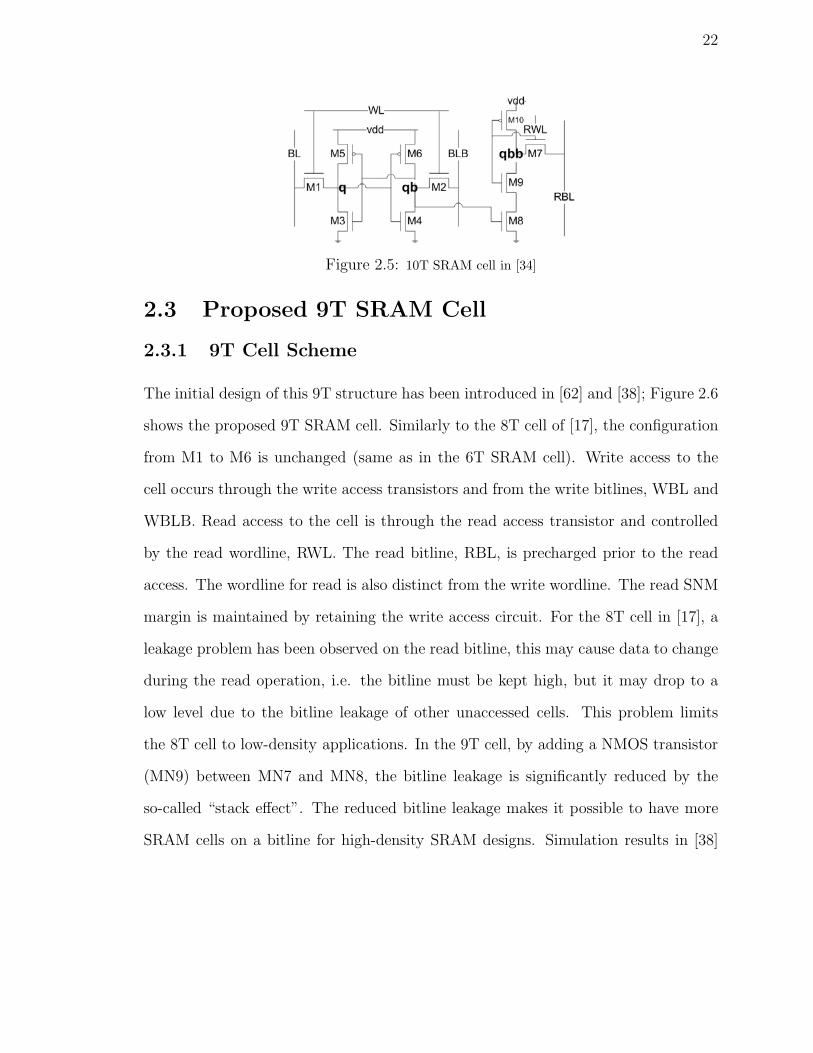
2.5 10T SRAM cell in [34] . . . . . . . . . . . . . . . . . . . . . . . . . . 22
2.6 Proposed 9T SRAM cell for low-power operation . . . . . . . . . . . . 23
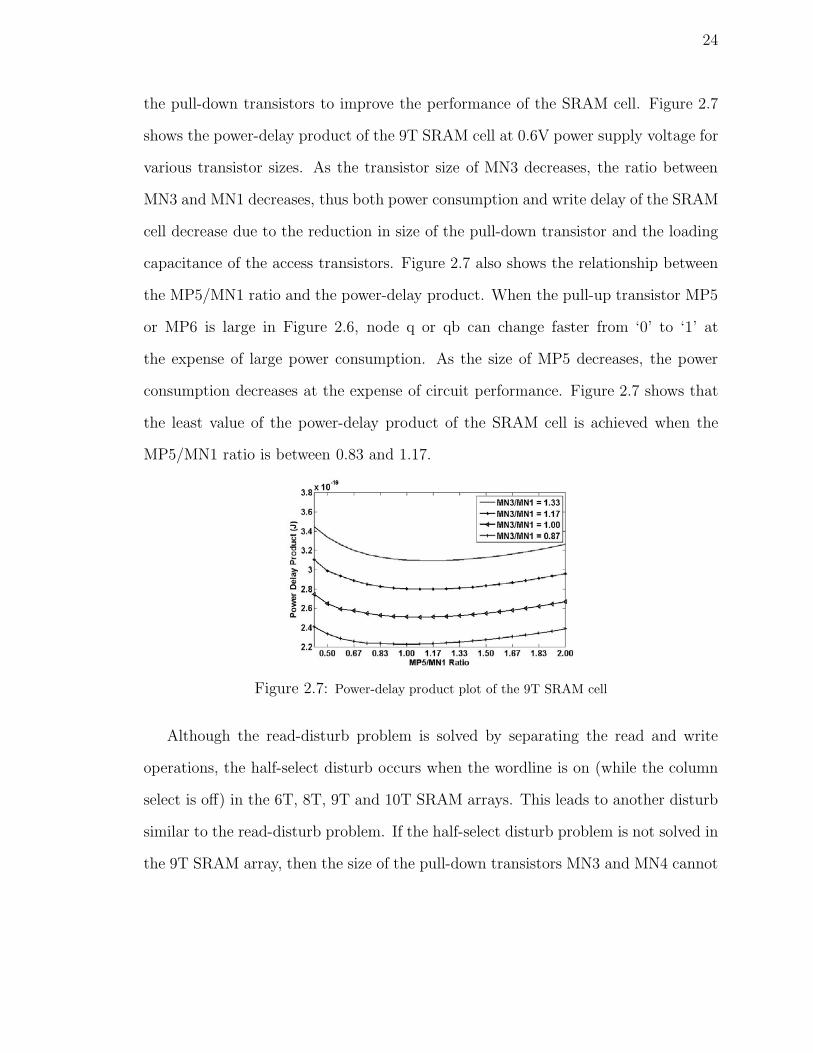
2.7 Power-delay product plot of the 9T SRAM cell . . . . . . . . . . . . . 24
2.8 Local write wordline generation scheme . . . . . . . . . . . . . . . . . 25
2.9 Butterfly plot and N-curve of the SRAM cell . . . . . . . . . . . . . . 28
2.10 N-curve of the 9T SRAM cell with different MN3/MN1 ratios . . . . 29
2.11 Write-trip current and critical charge of the 9T SRAM cell . . . . . . 31
2.12 Proposed 9T SRAM cell with transistor sizes in W/L (nm) . . . . . . 32
2.13 Layouts of a 3x2 cell array of the 6T SRAM cells . . . . . . . . . . . 33
2.14 Layouts of a 3x2 cell array of the proposed 9T SRAM cells . . . . . . 33
viii
2.15 Proposed write bitline balancing circuitry . . . . . . . . . . . . . . . . 35
2.16 Simulation results for the write operation of the proposed 9T SRAM
array . . . . . . . . . . . . . . . . . . . . . . . . . . . . . . . . . . . . 37
2.17 SPRs of different SRAM cells . . . . . . . . . . . . . . . . . . . . . . 39
2.18 Power-delay product of the SRAM cells at different temperatures and
power supplies for a) proposed 9T cell; b) 6T cell . . . . . . . . . . . 42
2.19 Power-delay product of the SRAM cells with the variations of mobility,
threshold voltage, and velocity saturation for proposed 9T cell . . . . 43
2.20 Power-delay product of the SRAM cells with the variations of mobility,
threshold voltage, and velocity saturation for 6T cell . . . . . . . . . 44
2.21 Power-delay product of the SRAM cells with channel length variations 45
2.22 Distribution of the SRAM cell power dissipation due to threshold volt-
age variations for a) 6T cell; b) proposed 9T cell . . . . . . . . . . . . 46
2.23 Power-delay product distributions of the 6T and the proposed 9T cell
due to process variations . . . . . . . . . . . . . . . . . . . . . . . . . 47
3.1 Cross sectional view of a carbon nanotube transistor (CNTFET) . . . 52
3.2 Top view of a carbon nanotube transistor (CNTFET) . . . . . . . . . 52
3.3 Equivalent circuit model for the intrinsic channel region of a CNTFET 53
3.4 Current-voltage (I-V) characteristics of a ballistic CNTFET . . . . . 54
3.5 Threshold voltage of P-type CNTFET with different chirality vectors 55
3.6 6T SRAM cell with CMOS . . . . . . . . . . . . . . . . . . . . . . . . 56
3.7 6T SRAM cell with CNTFET . . . . . . . . . . . . . . . . . . . . . . 56
3.8 MN4/MN2 ratio vs. voltage rise at nq for SRAM cells . . . . . . . . . 57
3.9 MP5/MN1 ratio vs. write voltage at q for SRAM cells . . . . . . . . 59
3.10 Static Noise Margin (SNM) of the SRAM cell with different PCNTFET
chirality vectors . . . . . . . . . . . . . . . . . . . . . . . . . . . . . . 62
3.11 Static Noise Margin (SNM) of the SRAM cell with different NCNTFET
chirality vectors . . . . . . . . . . . . . . . . . . . . . . . . . . . . . . 64
ix
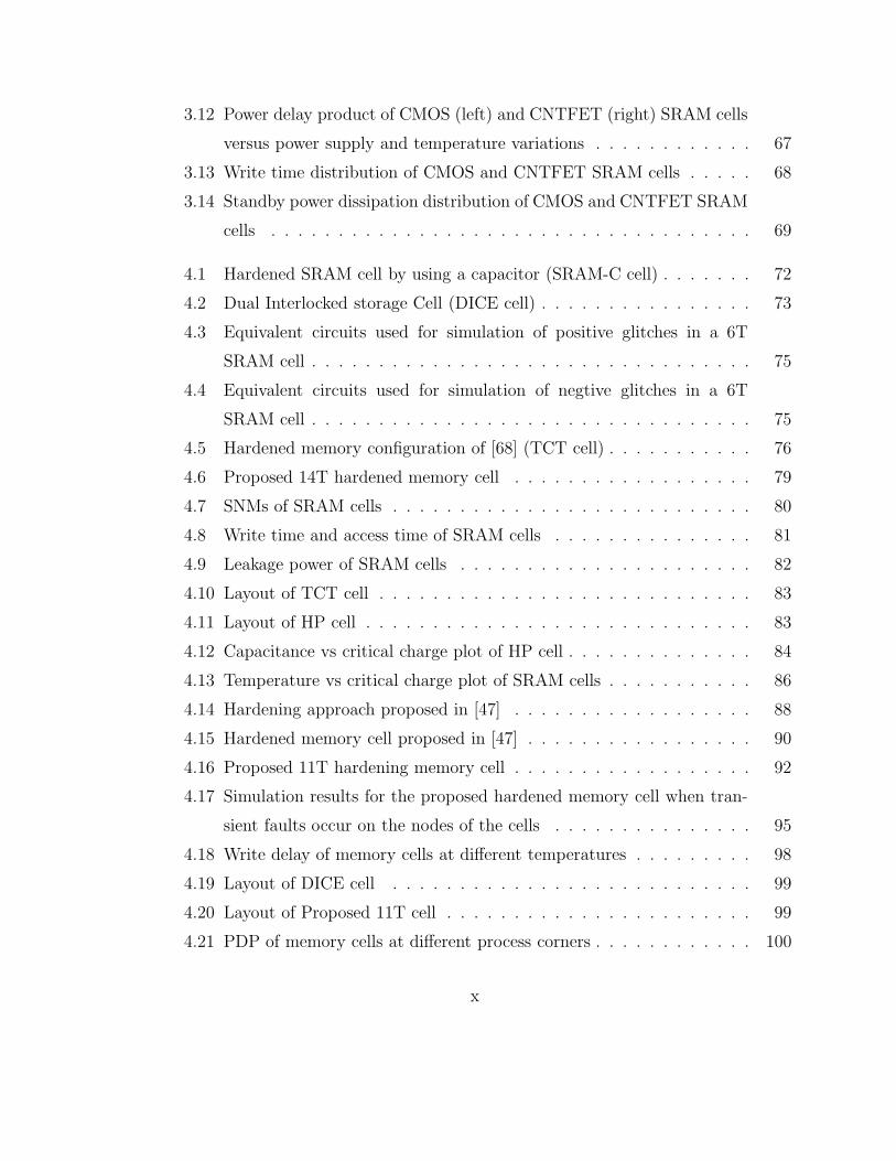
3.12 Power delay product of CMOS (left) and CNTFET (right) SRAM cells
versus power supply and temperature variations . . . . . . . . . . . . 67
3.13 Write time distribution of CMOS and CNTFET SRAM cells . . . . . 68
3.14 Standby power dissipation distribution of CMOS and CNTFET SRAM
cells . . . . . . . . . . . . . . . . . . . . . . . . . . . . . . . . . . . . 69
4.1 Hardened SRAM cell by using a capacitor (SRAM-C cell) . . . . . . . 72
4.2 Dual Interlocked storage Cell (DICE cell) . . . . . . . . . . . . . . . . 73
4.3 Equivalent circuits used for simulation of positive glitches in a 6T
SRAM cell . . . . . . . . . . . . . . . . . . . . . . . . . . . . . . . . . 75
4.4 Equivalent circuits used for simulation of negtive glitches in a 6T
SRAM cell . . . . . . . . . . . . . . . . . . . . . . . . . . . . . . . . . 75
4.5 Hardened memory configuration of [68] (TCT cell) . . . . . . . . . . . 76
4.6 Proposed 14T hardened memory cell . . . . . . . . . . . . . . . . . . 79
4.7 SNMs of SRAM cells . . . . . . . . . . . . . . . . . . . . . . . . . . . 80
4.8 Write time and access time of SRAM cells . . . . . . . . . . . . . . . 81
4.9 Leakage power of SRAM cells . . . . . . . . . . . . . . . . . . . . . . 82
4.10 Layout of TCT cell . . . . . . . . . . . . . . . . . . . . . . . . . . . . 83
4.11 Layout of HP cell . . . . . . . . . . . . . . . . . . . . . . . . . . . . . 83
4.12 Capacitance vs critical charge plot of HP cell . . . . . . . . . . . . . . 84
4.13 Temperature vs critical charge plot of SRAM cells . . . . . . . . . . . 86
4.14 Hardening approach proposed in [47] . . . . . . . . . . . . . . . . . . 88
4.15 Hardened memory cell proposed in [47] . . . . . . . . . . . . . . . . . 90
4.16 Proposed 11T hardening memory cell . . . . . . . . . . . . . . . . . . 92
4.17 Simulation results for the proposed hardened memory cell when tran-
sient faults occur on the nodes of the cells . . . . . . . . . . . . . . . 95
4.18 Write delay of memory cells at different temperatures . . . . . . . . . 98
4.19 Layout of DICE cell . . . . . . . . . . . . . . . . . . . . . . . . . . . 99
4.20 Layout of Proposed 11T cell . . . . . . . . . . . . . . . . . . . . . . . 99
4.21 PDP of memory cells at different process corners . . . . . . . . . . . . 100
x
4.22 Proposed 13T hardened memory cell . . . . . . . . . . . . . . . . . . 103
4.23 Timing diagram of the proposed 13T memory cell . . . . . . . . . . . 105
4.24 Critical charge plot on the critical pair for DICE cell, 11T hardened
cell and 13T hardened cell . . . . . . . . . . . . . . . . . . . . . . . . 107
4.25 Performance, power, and area comparison of the DICE, 11T and 13T
cells . . . . . . . . . . . . . . . . . . . . . . . . . . . . . . . . . . . . 108
4.26 Layout of Proposed 13T cell . . . . . . . . . . . . . . . . . . . . . . . 110
5.1 Equivalent circuits used for simulation of negtive (left) and positive
(right) glitches of latches . . . . . . . . . . . . . . . . . . . . . . . . . 116
5.2 Reference (unhardened) latch . . . . . . . . . . . . . . . . . . . . . . 117
5.3 A Schmitt trigger based hardening latch . . . . . . . . . . . . . . . . 118
5.4 A split internal node low-cost latch . . . . . . . . . . . . . . . . . . . 119
5.5 SER-tolerant path-exclusive latch . . . . . . . . . . . . . . . . . . . . 120
5.6 Modified soft error masking latch design . . . . . . . . . . . . . . . . 121
5.7 Proposed Schmitt trigger based latch . . . . . . . . . . . . . . . . . . 122
5.8 Cascode feedback Schmitt trigger (Cascode ST) latch . . . . . . . . . 123
5.9 Cascode M-SEM latch . . . . . . . . . . . . . . . . . . . . . . . . . . 124
5.10 Timing diagram of a level-sensitive latch . . . . . . . . . . . . . . . . 125
5.11 Layout of reference latch . . . . . . . . . . . . . . . . . . . . . . . . . 127
5.12 Layout of SEM-latch . . . . . . . . . . . . . . . . . . . . . . . . . . . 128
5.13 Layout of STPE latch . . . . . . . . . . . . . . . . . . . . . . . . . . 128
5.14 Layout of Modified SEM-latch . . . . . . . . . . . . . . . . . . . . . . 129
5.15 Layout of ST latch . . . . . . . . . . . . . . . . . . . . . . . . . . . . 129
5.16 Layout of Cascode ST latch . . . . . . . . . . . . . . . . . . . . . . . 130
5.17 Plot of power-delay product vs. critical charge for different latch designs133
5.18 Primary node charge versus secondary node charge of hardened latches 136
xi
Chapter 1
Introduction
1.1 Overview
Integrated circuit (IC) technology is the enabling technology for a whole host of
innovative devices and systems that have changed the way we live in the last five
decades. Integration allows us to build systems with many more transistors, allowing
much more computing power to be applied to solving a problem [75]. In the 1960s,
Gordon Moore, an industry pioneer, predicted that the number of transistors that
could be manufactured on a chip would grow exponentially. His prediction, now
known as Moore’s Law, reveals that integration complexity doubles approximately
every 1 to 2 years.
CMOS technology scaling has been enabling higher integration capacity in VLSI
designs. Over the last few years, devices at 45nm have been manufactured and the
deep sub-micron/nano range of 32nm is foreseen to be reached in the near future as
technology continues to scale down. In the 32nm technology era, the leakage current
has substantially increased, and the sensitivity to process variations in manufactur-
ing is considered to be almost unavoidable. Due to the lower Vdd and the smaller
1
2
node capacitance, the amount of charge stored on a circuit node is becoming increas-
ingly smaller, thus making circuits more susceptible to spurious voltage variations
caused by externally induced phenomena such as cosmic ray neutrons and α-particles
[53]. Therefore, robust CMOS circuits design techniques is becoming crucial in the
nanoscale era.
Technology boosters such as strain have helped the continuation of CMOS historic
performance trend up to 45nm node. As device physical gate length is reduced to
below 25nm at/beyond 65nm technology node, various leakage currents and device
parameter variation become the most important considerations for device optimiza-
tion. In fact, it can be argued that reduction of gate length below 25nm may not
offer the same advantage as short-gate devices had provided historically in terms of
power and performance at the system level [28]. The major detractors are: the lack
of a thin equivalent gate oxide (with low leakage current) for effective short channel
effect control, the increasing contribution of the fringing parasitic capacitance to the
total gate capacitance, and the rising contribution of the source/drain resistance to
the total device on-resistance [74]. Moreover, various device non-idealities cause the
I-V characteristics to be substantially different from well-tempered MOSFETs. It
becomes more difficult to further improve device/circuit performance by reducing the
physical gate length.
Therefore, new materials and devices have been investigated to replace silicon
in nanoscaled transistors from the year 2015 and beyond. As one of the promising
new devices, carbon nanotube transistors (CNTFETs) avoid most of the fundamen-
tal limitations for traditional silicon devices, due to their unique one-dimensional
band-structure that suppresses backscattering and makes near-ballistic operation a
3
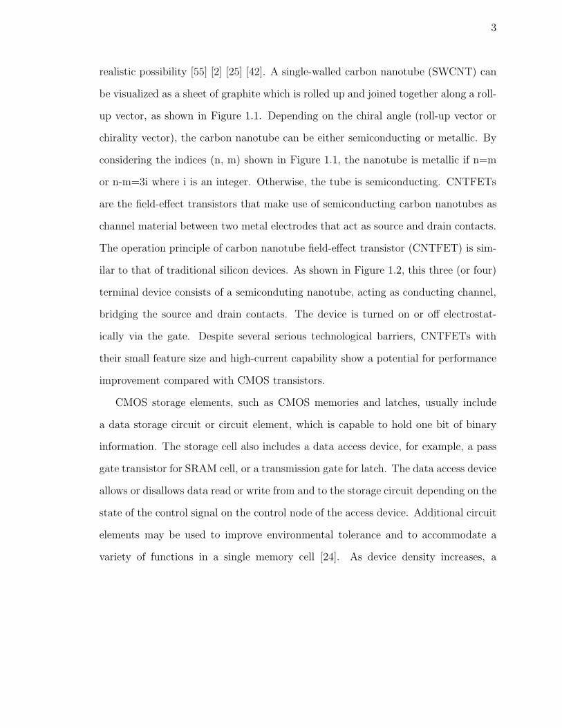
realistic possibility [55] [2] [25] [42]. A single-walled carbon nanotube (SWCNT) can
be visualized as a sheet of graphite which is rolled up and joined together along a roll-
up vector, as shown in Figure 1.1. Depending on the chiral angle (roll-up vector or
chirality vector), the carbon nanotube can be either semiconducting or metallic. By
considering the indices (n, m) shown in Figure 1.1, the nanotube is metallic if n=m
or n-m=3i where i is an integer. Otherwise, the tube is semiconducting. CNTFETs
are the field-effect transistors that make use of semiconducting carbon nanotubes as
channel material between two metal electrodes that act as source and drain contacts.
The operation principle of carbon nanotube field-effect transistor (CNTFET) is sim-
ilar to that of traditional silicon devices. As shown in Figure 1.2, this three (or four)
terminal device consists of a semiconduting nanotube, acting as conducting channel,
bridging the source and drain contacts. The device is turned on or off electrostat-
ically via the gate. Despite several serious technological barriers, CNTFETs with
their small feature size and high-current capability show a potential for performance
improvement compared with CMOS transistors.
CMOS storage elements, such as CMOS memories and latches, usually include
a data storage circuit or circuit element, which is capable to hold one bit of binary
information. The storage cell also includes a data access device, for example, a pass
gate transistor for SRAM cell, or a transmission gate for latch. The data access device
allows or disallows data read or write from and to the storage circuit depending on the
state of the control signal on the control node of the access device. Additional circuit
elements may be used to improve environmental tolerance and to accommodate a
variety of functions in a single memory cell [24]. As device density increases, a
4
Figure 1.1: Unrolled graphite sheet
larger fraction of chip area is devoted to the on-chip memory modules, because on-
chip memory helps improve the micro-architectural performance of a microprocessor.
Several of the latest processor designs showed that around 50% of the chip area was
occupied by caches [58], Meanwhile, latches and D flip-flops, which are the basic
building blocks of the sequential circuits, also take a large area of the latest chips.
Our work will focus on the analysis and design of robust storage elements in both
32nm CMOS technology and novel CNTFETs.
In this dissertation, we target the robust design of two major storage elements in
modern integrated circuits:
• memory cell
• latch

5
Figure 1.2: Cross section view of a CNTFET
Figure 1.3: Conventional 6T memory cell
1.1.1 Design Issues of robust SRAM cells
Figure 1.3 shows the conventional 6T memory cell, which is the fundamental building
block of a static RAM. The cell has a single wordline WL and two complementary
bitlines BL and BLB. The cell contains a pair of cross-coupled inverters and an access
transistor for each bitline. The data are stored on the cross-coupled inverters. If the
data is disturbed slightly, positive feedback around the loop will restore it to Vdd or
ground. The wordline is asserted to read or write the cell. The 6T cell is commonly
used in the modern SRAM design because of its compactness. In order to perform

6
correct read and write operation of the SRAM cell, the ratio between the pull down
NMOS N3 and access transistor N1, and the ratio between pull up PMOS P5 and
access transistor N1, need to be carefully designed. Prior to the read operation, the
bitlines BL and BLB are precharge to Vdd. When a SRAM cell is selected for read, the
access transistors N1 and N2 are ON. If the SRAM stores a ‘0’, the voltage on node
q is 0 and the voltage on node qb is Vdd, therefore N3 is ON and N4 is OFF. Devices
N3 and N1 form a voltage divider between the bitline BL and ground. Therefore, the
voltage on node q will rise to some voltage level and may turn on N4, discharging node
qb. To avoid this so called read-disturb problem, the ratio between the pull down
NMOS N3 and access transistor N1 should be kept greater than about 1.28 in the
CMOS 6T SRAM cell design [16]. Therefore, for the read operation, a minimum cell
ratio is required to prevent accidentally writing the SRAM cell. However, larger cell
ratios also make it harder to accomplish correct write operation. In order to perform
correct write operation, the pull up transistor should not be too strong. Assume
that the SRAM cell is storing ‘1’ and it is required to write a new data ‘0’ into the
SRAM cell. The node q in Figure 1.3 is going to be low, so the access transistor N1
must be significantly more conductive than the PMOS P5. In the traditional CMOS
design, the P5/N1 ratio should not be greater than 1.6 [16]. In this dissertation, the
transistor size of the 6T SRAM cell in Figure 1.3 is set to be 160nm/40nm (transistor
width/transistor length) for N3 and N4, 80nm/40nm for P5 and P6, 120nm/40nm for
N1 and N2. Besides the correct read and write operation, design issues like power,
delay, and stability are also very important in SRAM cell design, especially in the
nanoscale era, where leakage current and other short channel effects will introduce
severe impact on the SRAM cell. On the other hand, SRAM cells, which employ the
7
smallest transistors possible for density, are extremely sensitive to both systematic
and random process variations.
0 0.1 0.2 0.3 0.4 0.5 0.60
0.1
0.2
0.3
0.4
0.5
0.6
Input Voltage (V)
Ou
tpu
t V
olt
age
(V)
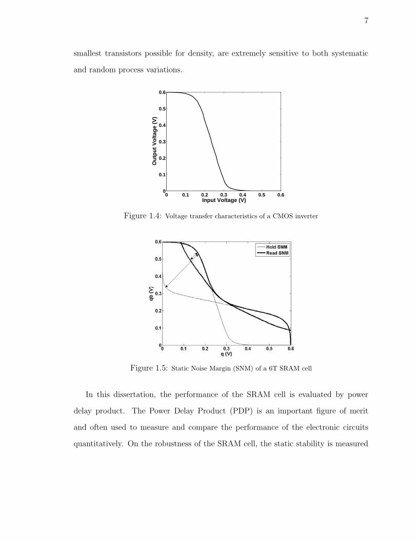
Figure 1.4: Voltage transfer characteristics of a CMOS inverter
Figure 1.5: Static Noise Margin (SNM) of a 6T SRAM cell
In this dissertation, the performance of the SRAM cell is evaluated by power
delay product. The Power Delay Product (PDP) is an important figure of merit
and often used to measure and compare the performance of the electronic circuits
quantitatively. On the robustness of the SRAM cell, the static stability is measured
8
by the Static Noise Margin (SNM) and dynamic stability of the memory cell which is
usually measured by critical charge. During the simulation of the SRAM cell, Monte
Carlo simulation, which is a computational algorithm that relys on repeated random
sampling to compute the simulation results, is used to investigated the impact of
random variations on SRAM robustness.
In a 6T SRAM cell, the data are stored on the cross-coupled inverters. Figure 1.4
shows the voltage transfer characteristics (VTC) of the inverter. The static stability of
the SRAM cell is measured by the SNM (the SNM is defined as the maximum value of
DC noise voltage that can be tolerated by the SRAM cell without changing the stored
bit [64]). The SNM of a SRAM cell is obtained by drawing the VTC of the inverter and
mirroring the VTC on the same plot, as shown in Figure 1.5. The maximum possible
square between the two-lobed curve, which is called “butterfly curve”, is graphically
determined on the plot, and used to determine the SNM. The SNM is defined as the
length of the side of the largest square that can be embedded inside the lobes of the
butterfly curve. Larger diagonal length means larger SNM. This is the most common
way of representing the SNM graphically for a SRAM cell holding data. As shown in
Figure 1.5, the worst case scenario of the cell static stability is when the cell is in read
operation. The internal node of the SRAM cell that stores a ‘0’ gets pulled up due
to the voltage divider from bitline to ground, which is called read disturb problem
mentioned above. This increase in voltage severely degrades the SNM during the
read operation (read SNM), as shown in Figure 1.5. The degradation of SNM limits
voltage scaling for SRAM designs. Many approaches have been proposed to improve
the SNM and will be discussed in the following chapters.
When a SRAM cell is holding data, a carbon or nitrogen atom can release a
9
neutron from the atom’s nucleus if a cosmic ray collides with oxygen. If such neutron
then collides with a silicon atom, it can split the atom’s nucleus into smaller charged
particles. Moreover, if the silicon atom is in a semiconductor memory, the charged
particles can change the contents of a memory cell, yielding a so-called “soft error”.
[7] With technology scaling, the soft-error rate is expected to be significantly higher
for deep submicron/nano SRAMs due to the lower Vdd and smaller node capacitance.
The critical charge (Qcrit) is a well-known parameter used in the soft-error domain
and is defined as the minimum charge collected by a node that makes an SRAM
cell flip [31]. It is related to the dynamic response of the memory cell to a dynamic
perturbation and is a useful parameter to evaluate its dynamic robustness. Impact
area is also very important factor during the dynamic robustness analysis, however,
in this dissertation, only critical charge is considered as the metric for the dynamic
robustness of the SRAM cell.
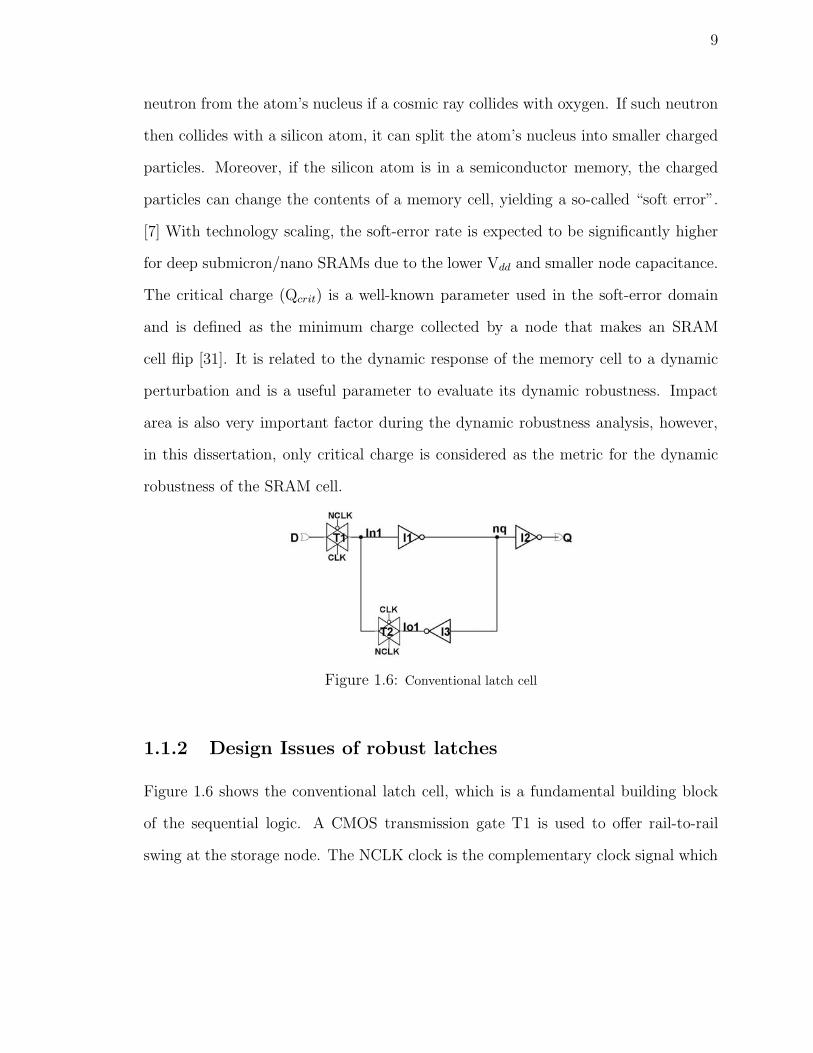
Figure 1.6: Conventional latch cell
1.1.2 Design Issues of robust latches
Figure 1.6 shows the conventional latch cell, which is a fundamental building block
of the sequential logic. A CMOS transmission gate T1 is used to offer rail-to-rail
swing at the storage node. The NCLK clock is the complementary clock signal which

10
can be locally generated from CLK through an inverter. When the clock CLK is ‘1’,
the input transmission gate T1 is ON, the feedback tristate is OFF, and the latch
is transparent. When the clock CLK is ‘0’, the input transmission gate T1 turns
OFF and the feedback tristate turns ON, holding ln1 at the correct level. When
determining the size of the latch cell, the driving strength of the transparent path
should be strong enough so that the data can be easily transferred from the data
input to output when clock CLK is ‘1’. Furthermore, the data must be held stable
for a minimum set-up of data input to the clock. Therefore, the inverter I1 is made to
be stronger than the feedback inverter I3 for performance and power consideration.
Similar to the 6T memory cell, the cross-coupled inverter configuration in the
latch cell is very vulnerable to soft errors in nanoscale era. α-particles and cosmic
ray particles is one of the important noise sources that may cause a storage node to
lose its state. Once a particle strikes a silicon, it generates electron-hole pairs along
its track, and some of them are collected by a nearby junction. The collected charge
causes a voltage change on the storage node. Hardening approaches such as increasing
the capacitance of the storage node can improve the robustness of the latch and the
hardening approaches will be discussed in this dissertation.
Besides robustness of the latch cells, the performance of the latches is also con-
sidered. The performance of the latches are compared based on simulations of the
switching characteristics of each latch for different values of data setup as proposed
in [78], i.e.
D = Tsetup +DC−Q (1.1.1)
DC−Q is the propagation delay of the latch from the clock signal CLK to the
11
output Q. Tsetup is the minimum time between a change in the data signal and the
trailing edge of the clock signal such that the new value of D can propagate to the
output Q of the latch and stored in the latch during the non-transparent phase. For
Tsetup and DC−Q, the max delay between positive and negative transitions (i.e. the
larger value between a high to low transition and a low to high transition) is selected
as the performance metric for latch.
1.2 Previous Work
One of the most serious threats to long-term SRAM viability in scaled processes is
cell static stability, how to maintain both cell read stability and write ability. The
read static noise margin (SNM) is often used as a measure of the cell read stability
[64]. Simulation has shown that the SNM of the conventional 6T cell shown in
Figure 1.3 degrades due to lower Vdd and larger variation at nanoscale. There are
a few techniques to extend the viability of the conventional 6T SRAM cell to lower
supply voltages and scaling. For example, lower bitline precharge voltage [9] and
boosted cell voltage [46] can improve read SNM. However, in the long term, whether
the 6T cell is the optimal cell topology choice in nanoscale processes is still an open
question. Several configurations have been proposed to improve the SNM by adding
separate read access structures to the original 6T configuration, thus making the
read SNM equal to the hold SNM [17], [8], and [34]. There are a number of attractive
alternate cell topologies that, while they do require more area and/or devices per cell,
may achieve higher overall bit density because they require less peripheral circuitry.
Besides traditional bulk CMOS based approach, using alternate or emerging tech-
nologies offers some promising solutions as well. For example, process variations
12
are less severe in SOI than in bulk CMOS [29], and FinFET-based SRAM cells can
offer improved characteristics [23]. Meanwhile, as the technology continues scaling
down, physical phenomena and technology limitations may prevent the continued
improvements in figures of merit such as low power and high reliability. Ballistic
transport operation and low off current make the CNTFET a suitable device for
high performance and increased integration density of SRAM design. Moreover, the
MOSFET-like model of the CNTFET is likely to be scalable down to 10nm channel
length, thus providing a substantial performance and power improvement compared
to the MOSFET model (with minimum channel length of 32nm [74]). Therefore,
a SRAM design implemented using CNTFETs requires a significantly smaller area
than its CMOS counterpart. A resistive-load CNTFET-based SRAM cell has been
proposed in [6].
With scaling, hard and soft errors in SRAM will increase in frequency and scope,
so that a single error event is more likely to cause failures on the storage elements,
such as memories and latches. There are a number of causes of soft errors including
energetic particle strikes, signal or power-supply noise coupling, and erratic device
behavior [53]. To combat hard and soft errors, designers currently employ a number
of techniques, including error-correcting codes (ECCs) [21], bit-interleaving [45], and
redundancy [76]. These hardening methods add system level overhead and power
dissipation. Design hardening techniques at circuit level can developed to achieve
immunity to upsets. They can avoid the error latency and performance loss of system
design hardening solutions. Hardened design approaches can be classified into two
broad categories [47]. In the first category, hardening is achieved in the design by
increasing the capacitance of some nodes, or the strength of the transistors through a

13
novel design. Such an approach must be scaled with the feature size of the employed
technology and may result in unwanted penalties with respect to performance (i.e.
an increase in delay) and power dissipation. For this category of hardening designs,
capacitors in SRAM cells can be utilized to absorb the excess charge [59] [68]. In
the second approach, the storage cells are designed to be insensitive to TFs, so in-
dependent of both the size of the cell’s transistors and the capacitance of the cell’s
nodes. These approaches have the advantage of technology independence, but they
may incur in a high design overhead due to the additional circuitry. An example
of the approach in the second category has been reported in [13] and is commonly
known as DICE.
Besides memory cells, data latches are used in latch chains and as separate logic
gates for data manipulation and storage and must have a good tolerance to soft
errors. Many error tolerant methods for soft errors occurring in latches of logic
circuits have been proposed. Approaches using Schmitt triggers and/or innovative
feedback arrangements are utilized to protect latches from transient faults [44] [63].
Another hardening approach employs a standard path-exclusive latch and a DICE-like
redundant clocked keeper to achieve a high SER-tolerance [26].
1.3 Dissertation Outline
As microprocessors are becoming larger and more complex, a larger portion of the
die is dedicated to caches and latches. The robustness of the storage elements is
very important as those storage elements that need to store correct data. SRAMs
comprise a significant percentage of the total area and total power for many digital
chips. Therefore, in the first three sections, the robust design of the memory cell will
14
be discussed.
In Chapter 2, a novel nine transistor (9T) CMOS SRAM cell design at 32nm
feature size is presented to improve the stability, power dissipation, and delay of the
conventional SRAM cell along with detailed comparisons with other designs. An op-
timal transistor sizing is established for the proposed 9T SRAM cell by considering
stability, energy consumption, and write-ability. As a complementary hardware solu-
tion at array-level, a novel write bitline balancing technique is proposed to reduce the
leakage current. A new metric that comprehensively captures all of these figures of
merit (and denoted to as SPR), is also proposed; under this metric, the proposed 9T
SRAM cell is shown to be superior to all other cell configurations found in the techni-
cal literatures. The impact of the process variations on the cell design is investigated
in detail.
In Chapter 3, instead of using CMOS, a new design of a highly stable and low-
power SRAM cell using carbon nanotube FETs (CNTFETs) that utilizes different
threshold voltages for best performance is proposed in this chapter. In a CNT, the
threshold voltage can be adjusted by controlling the chirality vector (i.e. the diam-
eter). In the proposed 6T SRAM cell design, while all CNTFETs of the same type
have the same chirality, N-type and P-type transistors have different chiralities, i.e.
a dual-diameter design of SRAM cell. The SPR metric is also used in this chapter
to captures figures of merit like stability, power dissipation and write time. Finally,
the sensitivity of the CNTFET SRAM design to process variations is assessed and
compared with its CMOS design counterpart.
Both Chapter 2 and Chapter 3 focus on improving the static stability, which is
measured by the static noise margin (SNM). In Chapter 4, dynamic stability of the

15
memory cell, which is usually measured by critical charge, is investigated. Higher
critical charge means better tolerance to soft errors for the memory cells. In this
chapter, a new 14T design for hardening CMOS memory cell at the nano feature size
of 32nm is proposed first. By separating the circuitry for the write and read oper-
ations, both static stability and dynamic stability of the proposed cell configuration
have increased compared with conventional designs. Another hardening approach,
which belongs to different category, is then proposed. The feedback loop of the pro-
posed hardened memory cell is blocked and by utilizing novel access and refreshing
mechanisms, the proposed 11T memory cell is totally tolerance to single node upset.
Multiple node upset analysis is then performed on the hardened memory cells and a
novel 13T memory cell configuration is proposed, analyzed, and simulated to show
a better tolerance to the likely multiple node upset, i.e. a transient or soft fault af-
fecting two nodes in a cell. Monte Carlo simulation confirms the excellent multiple
node upset tolerance of the proposed 13T hardened storage elements in the presence
of process, voltage, and temperature variations in their designs.
As another major storage element in the VLSI circuit design, hardened latch
design has also been investigated in our work. Three new hardened designs for CMOS
latches at 32nm feature size are proposed in this dissertation; two of these circuits
are Schmitt trigger based, while the third one utilizes a cascode configuration in the
feedback loop. A novel design metric (QPAR) for latches is introduced to assess the
overall design effectiveness such as area, performance, power, and soft error tolerance.
Multiple node upset analysis is also performed on the hardened latches and the results
show that the hardened latches with a high critical charge have a better multiple node
upset tolerance.

16
Finally, Chapter 6 summarizes the key findings and contributions of this disser-
tation, and proposes some recommendations for future work.
Chapter 2
Analysis and Design of CMOSSRAM Cell for Low Leakage andHigh Stability
2.1 Introduction
Advances in chip design using CMOS technology have made it possible to design very
dense chips that deliver high performance at low power consumption. To achieve
these objectives, the feature size of CMOS devices has been dramatically scaled to
smaller dimensions. Over the last few years, devices at 45nm have been manufactured
and the deep sub-micron/nano range of 32nm is foreseen to be reached in the near
future as technology continues to scale down.
Power and density have become the key limitations in many designs as nanoscale
devices are becoming a reality at rapid pace. Today’s high performance integrated
circuits consume more than 40% of the total active mode power due to leakage cur-
rents. Furthermore, leakage is the only source of power consumption in idle circuit.
For the foreseeable future, SRAM will likely remain the embedded memory technol-
ogy of choice for many microprocessors and systems on chips (SoC) due to its speed
17
18
and compatibility with standard logic processes [11]. With the advent of SoC, the
design of power efficient SRAM structures has become highly desirable. One of the
most effective approaches to meet this objective is to design SRAM cells that oper-
ate in ultra-low power mode. The decrease in supply voltage reduces the dynamic
power quadratically and the leakage power is reduced linearly to the first order [35].
However, with an aggressive scaling in technology as predicted by the Industry Tech-
nology Roadmap (ITR), substantial problems have already been encountered when
the conventional six transistors (6T) SRAM cell configuration is utilized at an ultra-
low power supply, because this cell shows poor stability at very small feature sizes.
Moreover, the small static noise margin makes the memory susceptible to radiation
and errors in data retention. SRAM cell configurations with more than six transistors
to reduce leakage power and improve stability have been proposed in [17], [8], and
[34]. An 8T cell [17] employs two more transistors to access the read bitline. Two
additional transistors (thus yielding 10T cell designs) are employed in [8] and [34] to
reduce the leakage current. However, those previous researches still do not provide
a complete viable solution for low power application on nanoscale technology due to
leakage power, cell area overhead, and stability issues.
In this chapter, a nine transistors (9T) SRAM cell is presented, and the presented
9T SRAM cell is more amenable than previous configurations to small feature sizes
encountered in deep sub-micron/nano bulk CMOS technology. Simulations have been
performed using Berkeley Predictive Technology Model at 32nm [52]. Compared with
the 8T and 10T cells of [17], [8], and [34], the proposed 9T scheme offers significant
advantages in terms of power consumption and leakage. An optimal transistor sizing
is found for the proposed 9T SRAM cell to increase stability and critical charge, thus
19
tolerating soft errors. An innovative precharging and bitline balancing scheme for the
write operation of the 9T SRAM cell is utilized for maximum standby power savings
in a memory array. A novel metric that comprehensively captures all of these figures
of merit is also proposed and used for comparison.
2.2 Review of SRAM Cells
2.2.1 Conventional 6T Cell
The conventional SRAM cell consists of 6 transistors (6T) as shown in Figure 2.1.
Issues regarding process variations and power supply voltages have been reported
for this type of cell [8]. The conventional 6T SRAM cell has been found to be
rather unstable for deep sub-micron/nano scale technology. This cell fails to meet
the operational requirements due to the low read Static Noise Margin (SNM). When
the conventional SRAM cell is in the read operation, the pass gate is turned on and
pulls the node that stores the logic ‘0’ (for example, the node identified by qb in
Figure 2.1) to a non-zero value. This decreases the read SNM, especially when a low
power supply voltage is utilized. Figure 2.2 shows the hold and read butterfly plot
for a 6T SRAM cell at 0.6V. As shown in this figure, the read SNM is very low and is
not acceptable for most memory designs. Several configurations have been proposed
to improve the SNM by adding separate read access structures to the original 6T
configuration, thus making the read SNM equal to the hold SNM [17], [8], and [34].
2.2.2 8T and 10T Cell
To address the reduced read SNM problem, the read and write operations are sep-
arated by adding read access structures to the original 6T cell, thus increasing the

20
Figure 2.1: Conventional 6T SRAM cell and its worst-case stability condition
Figure 2.2: Hold and read butterfly plot of the conventional 6T SRAM cell at power supply voltageof 0.6V
transistor count to eight. As the read current does not significantly affect the cell
value, the read stability of the 8T cell [17], as shown in Figure 2.3, is dramatically
increased compared with the original 6T SRAM cell. By using this cell, the read
SNM is only determined by the two cross-coupled inverters. The worst-case stability
condition encountered previously in a 6T SRAM cell is avoided and a high read SNM
is retained. Therefore, the 8T cell has a higher read SNM than the 6T SRAM cell.
However, for the 8T structure, the read bitline leakage is significant, especially in the
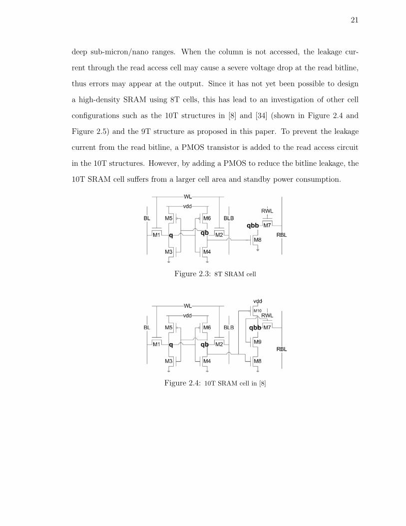
21
deep sub-micron/nano ranges. When the column is not accessed, the leakage cur-
rent through the read access cell may cause a severe voltage drop at the read bitline,
thus errors may appear at the output. Since it has not yet been possible to design
a high-density SRAM using 8T cells, this has lead to an investigation of other cell
configurations such as the 10T structures in [8] and [34] (shown in Figure 2.4 and
Figure 2.5) and the 9T structure as proposed in this paper. To prevent the leakage
current from the read bitline, a PMOS transistor is added to the read access circuit
in the 10T structures. However, by adding a PMOS to reduce the bitline leakage, the
10T SRAM cell suffers from a larger cell area and standby power consumption.
Figure 2.3: 8T SRAM cell
Figure 2.4: 10T SRAM cell in [8]
22
Figure 2.5: 10T SRAM cell in [34]
2.3 Proposed 9T SRAM Cell
2.3.1 9T Cell Scheme
The initial design of this 9T structure has been introduced in [62] and [38]; Figure 2.6
shows the proposed 9T SRAM cell. Similarly to the 8T cell of [17], the configuration
from M1 to M6 is unchanged (same as in the 6T SRAM cell). Write access to the
cell occurs through the write access transistors and from the write bitlines, WBL and
WBLB. Read access to the cell is through the read access transistor and controlled
by the read wordline, RWL. The read bitline, RBL, is precharged prior to the read
access. The wordline for read is also distinct from the write wordline. The read SNM
margin is maintained by retaining the write access circuit. For the 8T cell in [17], a
leakage problem has been observed on the read bitline, this may cause data to change
during the read operation, i.e. the bitline must be kept high, but it may drop to a
low level due to the bitline leakage of other unaccessed cells. This problem limits
the 8T cell to low-density applications. In the 9T cell, by adding a NMOS transistor
(MN9) between MN7 and MN8, the bitline leakage is significantly reduced by the
so-called “stack effect”. The reduced bitline leakage makes it possible to have more
SRAM cells on a bitline for high-density SRAM designs. Simulation results in [38]

23
have shown that 512 bitcells can be connected to the same bitline for 9T SRAM cell
case while only 32 8T SRAM cells can be connected to one bitline at 0.6V power
supply. With more bitcells on one bitline, less peripheral circuits are needed in the
9T SRAM array design. Therefore, the area of the 9T SRAM block is reduced.
Figure 2.6: Proposed 9T SRAM cell for low-power operation
For high density memory design, the SRAM cell should be sized as small as possi-
ble. However, for correct operation a sizing constraint is applied to the conventional
6T SRAM cell shown in Figure 2.1, i.e. the pull-down to the pass gate transistors
ratio must be greater than 1.2 to avoid the read-upset problem [16]. However, in
the 9T SRAM cell case, when the read is enabled (RWL=1), the read bitline (RBL)
is conditionally discharged through the pull-down transistors MN7, MN9, and MN8
depending on the data stored at node qb. The cell node is isolated from the bitline
during the read operation, and it retains the hold mode SNM. Therefore, the tran-
sistor ratio between MN3 and MN1 can be decreased to achieve better performance.
As the pull-down transistors (MN3 and MN4) are the largest transistors, a significant
amount of power is saved by scaling down these transistors. As the loading capaci-
tance of the access transistors (MN1 and MN2) decreases, the write delay will also
be decreased. At the same time, the write-ability will be strengthened as the ratio
between the access transistor and the pull-down transistor is increased.
The power-delay product is commonly used to show the impact of decreasing
24
the pull-down transistors to improve the performance of the SRAM cell. Figure 2.7
shows the power-delay product of the 9T SRAM cell at 0.6V power supply voltage for
various transistor sizes. As the transistor size of MN3 decreases, the ratio between
MN3 and MN1 decreases, thus both power consumption and write delay of the SRAM
cell decrease due to the reduction in size of the pull-down transistor and the loading
capacitance of the access transistors. Figure 2.7 also shows the relationship between
the MP5/MN1 ratio and the power-delay product. When the pull-up transistor MP5
or MP6 is large in Figure 2.6, node q or qb can change faster from ‘0’ to ‘1’ at
the expense of large power consumption. As the size of MP5 decreases, the power
consumption decreases at the expense of circuit performance. Figure 2.7 shows that
the least value of the power-delay product of the SRAM cell is achieved when the
MP5/MN1 ratio is between 0.83 and 1.17.
Figure 2.7: Power-delay product plot of the 9T SRAM cell
Although the read-disturb problem is solved by separating the read and write
operations, the half-select disturb occurs when the wordline is on (while the column
select is off) in the 6T, 8T, 9T and 10T SRAM arrays. This leads to another disturb
similar to the read-disturb problem. If the half-select disturb problem is not solved in
the 9T SRAM array, then the size of the pull-down transistors MN3 and MN4 cannot

25
be reduced for better power-delay product performance because the read-disturb still
exists. A hardware-based approach proposed in [32] utilizes local write wordlines that
are only selected when the write control for the selected block is on. Figure 2.8 shows
the conceptual circuit scheme and waveforms of the proposed approach. The local
write wordline WWL is generated by the global write wordline signal WWLB and
the block select signal BSB. The write access transistors are only accessed when the
block is selected for write (BSB is low). Therefore, the local write wordlines are only
selected when the write control for the selected block is on, which avoids disturbing
un-selected cells on an accessed row for a write operation.
Figure 2.8: Local write wordline generation scheme
Compared with the 6T differential SRAM, the 9T SRAM cell requires a single
ended read port due to the separate read buffer. A single ended read operation
requires a larger voltage swing at the read bitline and it provides a larger noise
margin. For the 6T SRAM cell array, the differential bitlines must be precharged to
Vdd by the starting time of clock cycle and one of the bitlines needs to be discharged in
every read cycle. However, for the single ended read bitline, the bitline is discharged
26
only when state ‘1’ is read out. Therefore, the transient probability of the bitline is
reduced to half of the conventional SRAM, which reduces the switching power of the
single ended bitline. In the SRAM design with differential bitlines, the sense point
is set to 50mV, which is significantly lower than the sense point of the single end
bitline (half Vdd). However, most cells will discharge the bitline at more than 50mV.
[48] shows that the average voltage difference between two bitlines is 80% of Vdd.
Therefore, the dynamic power of the differential SRAM, for example a 6T SRAM cell
array, is higher than a single ended SRAM. The simulation results of [48] have shown
that the readout power of the differential SRAM array is 25% higher than the single
end SRAM array. Furthermore, as the 9T SRAM array allows more bitcells on one
bitline, the area and power consumption of the peripheral circuits of the 9T SRAM
array are significantly lower than for the 6T SRAM array.
The read operation is important for high performance SRAM design. A 512-row,
128-column cell array has been designed to measure the read access time. For the 6T
cell, the read access time is the time required for developing 50mV bitline differential
voltage after the wordline is turned on during a read operation [35]. For the 9T cell,
the read access time is the time required for discharging the bitline voltage to half Vdd
after the wordline is turned on during a read operation. HSPICE simulation shows
that the read access time of the 6T SRAM cell is 74.60ps while the read access time
of the 9T SRAM cell is 82.04ps (at 0.6V power supply voltage [38]). The single ended
configuration in the proposed 9T SRAM cell results in a 10% degradation of readout
time.
27
2.3.2 Data Stability and Write-ability
2.3.2.1 Static Noise Margin and Write-ability
The pull-down transistors (MN3 and MN4) are scaled down to reduce power con-
sumption in the previous section, however, they cannot be scaled down too much
due to the stability considerations. Proper data retention strength is necessary for
the SRAM cell, especially for the proposed 9T cell to operate at ultra-low power
supply. The stability of SRAM cell is usually represented by the SNM (the SNM
is defined as the maximum value of DC noise voltage that can be tolerated by the
SRAM cell without changing the stored bit [64] [12]). The static noise margin (SNM)
can be graphically found on the butterfly curve shown in Figure 2.9. Its drawback is
the inability to measure the SNM with automatic inline testers directly because the
SNM still has to be derived by mathematical manipulation of the measured data after
measuring the butterfly curves of the cell. An alternative method to characterize the
SRAM stability is based on the N-curve of the cell measured by inline testers [73]
[22]. The typical N-curve of the SRAM cell is measured by reading the input current
at the internal storage node and by sweeping the storage node voltage from 0V to
Vdd.
Two common metrics for the SRAM cell static noise margin are the static voltage
noise margin (SVNM) and the static current noise margin (SINM), and they are found
on the N-curve in Figure 2.10. At three points (A, B, and C) of the N-curve, the
current at the internal storage node q is zero. A and C correspond to the two stable
points of the butterfly curve, while B corresponds to the meta-stable point on the
N-curve. When the points A and B coincide, then the cell is at the edge of stability.
The voltage difference between the points A and B indicates the maximum tolerable
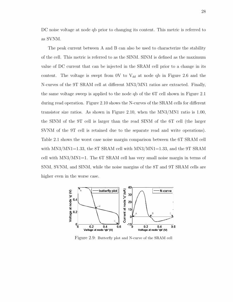
28
DC noise voltage at node qb prior to changing its content. This metric is referred to
as SVNM.
The peak current between A and B can also be used to characterize the stability
of the cell. This metric is referred to as the SINM. SINM is defined as the maximum
value of DC current that can be injected in the SRAM cell prior to a change in its
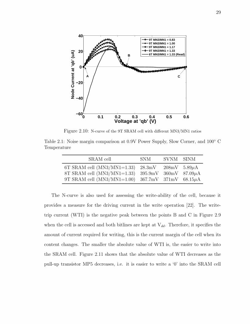
content. The voltage is swept from 0V to Vdd at node qb in Figure 2.6 and the
N-curves of the 9T SRAM cell at different MN3/MN1 ratios are extracted. Finally,
the same voltage sweep is applied to the node qb of the 6T cell shown in Figure 2.1
during read operation. Figure 2.10 shows the N-curves of the SRAM cells for different
transistor size ratios. As shown in Figure 2.10, when the MN3/MN1 ratio is 1.00,
the SINM of the 9T cell is larger than the read SINM of the 6T cell (the larger
SVNM of the 9T cell is retained due to the separate read and write operations).
Table 2.1 shows the worst case noise margin comparison between the 6T SRAM cell
with MN3/MN1=1.33, the 8T SRAM cell with MN3/MN1=1.33, and the 9T SRAM
cell with MN3/MN1=1. The 6T SRAM cell has very small noise margin in terms of
SNM, SVNM, and SINM, while the noise margins of the 8T and 9T SRAM cells are
higher even in the worse case.
Figure 2.9: Butterfly plot and N-curve of the SRAM cell
29
0 0.1 0.2 0.3 0.4 0.5 0.6−60
−40
−20
0
20
40
Voltage at ’qb’ (V)
No
de
Cu
rren
t at
’qb
’ (u
A)
9T MN3/MN1 = 0.839T MN3/MN1 = 1.009T MN3/MN1 = 1.179T MN3/MN1 = 1.336T MN3/MN1 = 1.33 (Read)
A
B
C
Figure 2.10: N-curve of the 9T SRAM cell with different MN3/MN1 ratios
Table 2.1: Noise margin comparison at 0.9V Power Supply, Slow Corner, and 100◦ CTemperature
SRAM cell SNM SVNM SINM
6T SRAM cell (MN3/MN1=1.33) 28.3mV 208mV 5.89μA8T SRAM cell (MN3/MN1=1.33) 395.9mV 360mV 87.09μA9T SRAM cell (MN3/MN1=1.00) 367.7mV 371mV 68.15μA
The N-curve is also used for assessing the write-ability of the cell, because it
provides a measure for the driving current in the write operation [22]. The write-
trip current (WTI) is the negative peak between the points B and C in Figure 2.9
when the cell is accessed and both bitlines are kept at Vdd. Therefore, it specifies the
amount of current required for writing, this is the current margin of the cell when its
content changes. The smaller the absolute value of WTI is, the easier to write into
the SRAM cell. Figure 2.11 shows that the absolute value of WTI decreases as the
pull-up transistor MP5 decreases, i.e. it is easier to write a ‘0’ into the SRAM cell
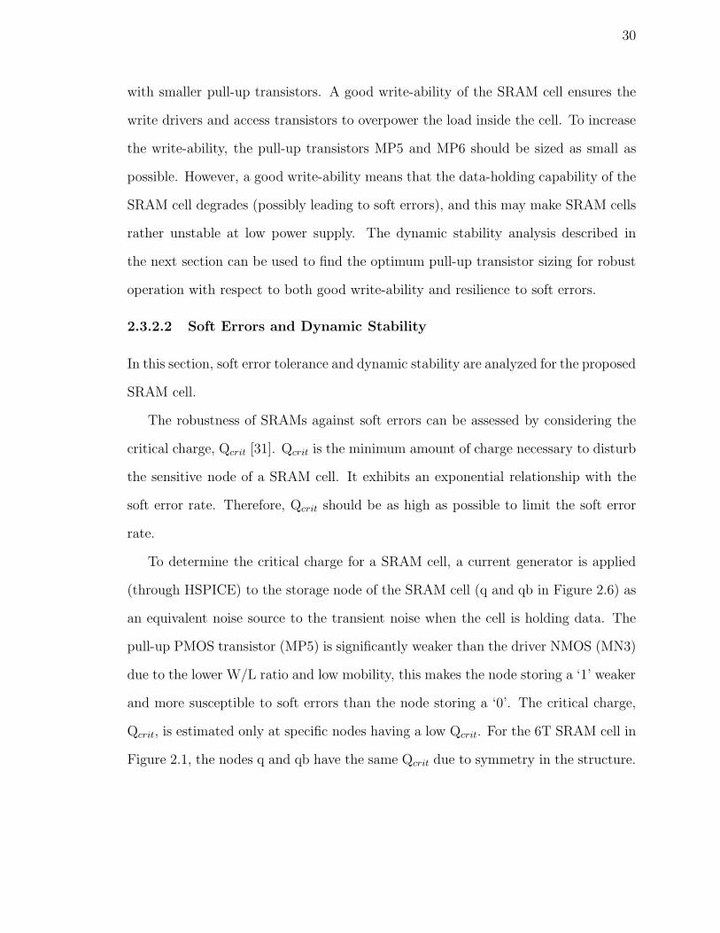
30
with smaller pull-up transistors. A good write-ability of the SRAM cell ensures the
write drivers and access transistors to overpower the load inside the cell. To increase
the write-ability, the pull-up transistors MP5 and MP6 should be sized as small as
possible. However, a good write-ability means that the data-holding capability of the
SRAM cell degrades (possibly leading to soft errors), and this may make SRAM cells
rather unstable at low power supply. The dynamic stability analysis described in
the next section can be used to find the optimum pull-up transistor sizing for robust
operation with respect to both good write-ability and resilience to soft errors.
2.3.2.2 Soft Errors and Dynamic Stability
In this section, soft error tolerance and dynamic stability are analyzed for the proposed
SRAM cell.
The robustness of SRAMs against soft errors can be assessed by considering the
critical charge, Qcrit [31]. Qcrit is the minimum amount of charge necessary to disturb
the sensitive node of a SRAM cell. It exhibits an exponential relationship with the
soft error rate. Therefore, Qcrit should be as high as possible to limit the soft error
rate.
To determine the critical charge for a SRAM cell, a current generator is applied
(through HSPICE) to the storage node of the SRAM cell (q and qb in Figure 2.6) as
an equivalent noise source to the transient noise when the cell is holding data. The
pull-up PMOS transistor (MP5) is significantly weaker than the driver NMOS (MN3)
due to the lower W/L ratio and low mobility, this makes the node storing a ‘1’ weaker
and more susceptible to soft errors than the node storing a ‘0’. The critical charge,
Qcrit, is estimated only at specific nodes having a low Qcrit. For the 6T SRAM cell in
Figure 2.1, the nodes q and qb have the same Qcrit due to symmetry in the structure.
31
However, in the 9T SRAM cell proposed in Figure 2.6, the node with the lowest Qcrit
is node q due to asymmetry in the 9T cell configuration.
Therefore, a current generator is applied to the node storing a ‘1’ to determine
the critical charge Qcrit in the worst case. The minimum total charge Qcrit can be
found by finding the integrated current applied to the node storing a ‘1’ to change
the content of the cell. Figure 2.11 shows the critical charge of the 9T SRAM cell for
different MP5/MN1 ratios.
0.4 0.5 0.6 0.7 0.8 0.9 1 1.10.5
1
1.5
2
MP5/MN1 Ratio
Cri
tica
l Ch
arg
e (f
C)
0.4 0.5 0.6 0.7 0.8 0.9 1 1.11.5
1
0.5
0
Wri
te−T
rip
−Cu
rren
t (u
A)
Write−Trip−Current
Critical Charge
Figure 2.11: Write-trip current and critical charge of the 9T SRAM cell
The tolerance of a SRAM cell to soft errors is enhanced by increasing the pull-up
transistor size. It is important to find the pull-up transistor size by considering the
conflicting constraint of write-ability and dynamic stability of the cell. As shown in
Figure 2.11, if a good write-ability is desired, the MP5/MN1 ratio should be as small
as possible. However, if good soft error immunity is desired, the MP5/MN1 ratio
should be as large as possible. However, MP5/MN1 is related to other design metrics
such as power delay product, critical charge, write-trip current, and area. In this
proposed design, to find the optimal design points considering all the design metrics
mentioned above using the simulation data shown in Figure 2.7 and Figure 2.11, the

32
proposed 9T SRAM cell uses the MP5/MN1 ratio of 0.67 to retain a high critical
charge (compared to a cell with very weak pull-up transistors) and a low absolute
value of WTI (compared to a cell with very strong pull-up transistors).
For the proposed 9T SRAM cell at 32nm feature size, this section has established
the transistor size ratios (between the pull-up PMOS, the pull-down NMOS, and
the access transistors) for low-power, best static and dynamic stability, and write-
ability. These figures of merit (power, stability, and performance) are optimized in the
proposed 9T SRAM cell when MP5/MN1 = 0.67 and MN3/MN1 = 1.00. Figure 2.12
shows the 9T SRAM cell with the transistor sizes found in this section.
Figure 2.12: Proposed 9T SRAM cell with transistor sizes in W/L (nm)
2.3.2.3 Area
The layouts of the conventional 6T and 9T SRAM cells are drawn based on MOSIS
deep sub-micrometer design rules [66] as shown in Figure 2.13 and Figure 2.14. For
the 6T SRAM cell shown in Figure 2.1, the ratio of 1.33 is used for M3 and M1,
and M1 and M5 have the same sizes as MN1 and MP5 shown in Figure 2.6 and
Figure 2.12. In Figure 2.13 and Figure 2.14, 3x2 SRAM cell arrays of 6T and 9T
SRAM cells are shown to demonstrate that the SRAM cell can be integrated into an
array design. General scaling has been applied to the MOSIS rule to scale the area of
the SRAM cells to 32nm feature size by a factor of 1/S2. With the scaling factor, the

33
area of the 6T cell layout at a 32nm feature size is 0.1899μm2, while the area of the
proposed 9T SRAM cell with optimal sizing at 32nm feature size is 0.2331μm2. The
area of the proposed 9T SRAM cell is increased by 22% comparing to 6T SRAM cell
when the previously described transistor sizing process is used. The area increase is
not due to the additional read bit line but to the additional transistors. The area of
the proposed 9T SRAM cell is exactly same as the 8T SRAM cell.
Figure 2.13: Layouts of a 3x2 cell array of the 6T SRAM cells
Figure 2.14: Layouts of a 3x2 cell array of the proposed 9T SRAM cells
In the traditional differential SRAM, a large area overhead is accounted due to the
differential sense amplifiers (compared with the single ended design). In the single
ended design, the readout circuit only consists of an inverter and a compensation
keeper [48]. Furthermore, the proposed 9T SRAM cell is designed for low-power
34
supply and high-density. As reported in [38], both 10T cell in [8] and the proposed
9T cell can be used in high-density memory designs to reduce the area overhead due
to the peripheral circuitry. Compared with its 10T cell counterparts, the 9T SRAM
cell has an area reduction of 16.7%, which makes the proposed 9T cell configuration
viable for high-density design. Therefore, in the proposed 9T SRAM design, less
peripheral circuits are required and the overall area is saved.
2.3.2.4 Standby Power Reduction
In a short channel device, the drain-induced barrier lowering (DIBL) has a significant
impact on the subthreshold current. Moreover, the source and drain depletion width
in the vertical direction and the source drain potential have a strong effect on the
band bending over a significant portion of the device. Consequently, the threshold
voltage and the subthreshold current of short-channel devices vary with the drain
bias. This effect is referred to as DIBL [1] [60]. When a high drain voltage is applied
to a short-channel device, it lowers the barrier height, resulting in a further decrease
of the threshold voltage. As the threshold voltage decreases, the subthreshold leakage
current increases exponentially. DIBL is enhanced at high drain voltages and shorter
channel lengths. When the 9T SRAM cell in Figure 2.6 stores ‘0’ (this is the worst-
case leakage current scenario for the 9T SRAM cell), the sub-threshold current of
MN1 is very high due to the large voltage difference between WBL and node q. This
leakage current can be reduced by lowering the voltage at WBL.
In a conventional 6T SRAM design, following a write operation, both bitlines must
be restored to Vdd to ensure a successful read operation. The write amplifier circuitry
of [16] ensures that the selected bitline is back to a “high” value by generating a
negative pulse to precharge the selected bitline high after driving the bitline low to
35
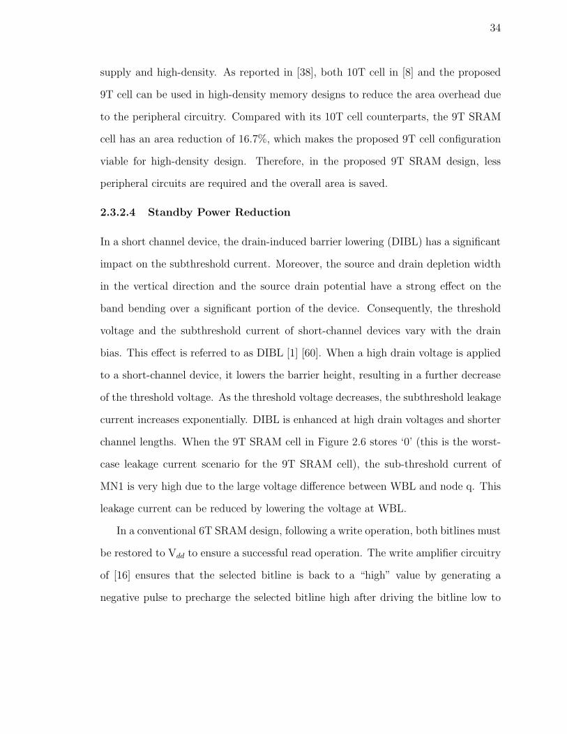
Figure 2.15: Proposed write bitline balancing circuitry
write ‘0’ into the SRAM cell. Therefore, both bitlines (WBL andWBLB in Figure 2.6)
will be restored to a “high” state after the write operation. When the SRAM cell
stores a ‘0’, the voltage difference between the drain and source of MN1 is Vdd, i.e. a
large subthreshold current from WBL to ground will be present when the SRAM cell
is in the standby mode.
The subthreshold current from WBL to ground can be reduced exponentially
by lowering the voltage at WBL in the standby mode. In this paper, the 9T cell
configuration is complemented with a solution at circuit-level for bitline balancing.
The new “write bitline balancing” circuitry is shown in Figure 2.15. Figure 2.16
shows the simulation results at a power supply voltage of 0.6V. When the WR EN
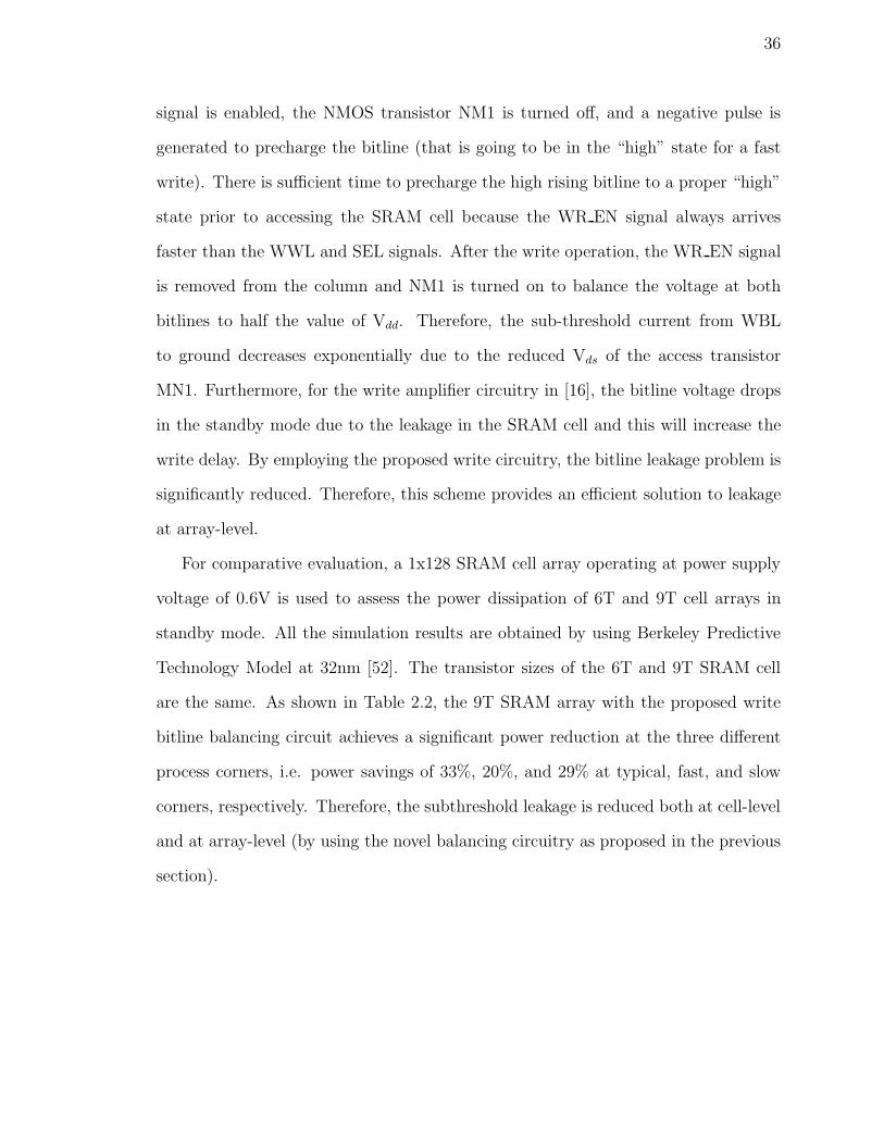
36
signal is enabled, the NMOS transistor NM1 is turned off, and a negative pulse is
generated to precharge the bitline (that is going to be in the “high” state for a fast
write). There is sufficient time to precharge the high rising bitline to a proper “high”
state prior to accessing the SRAM cell because the WR EN signal always arrives
faster than the WWL and SEL signals. After the write operation, the WR EN signal
is removed from the column and NM1 is turned on to balance the voltage at both
bitlines to half the value of Vdd. Therefore, the sub-threshold current from WBL
to ground decreases exponentially due to the reduced Vds of the access transistor
MN1. Furthermore, for the write amplifier circuitry in [16], the bitline voltage drops
in the standby mode due to the leakage in the SRAM cell and this will increase the
write delay. By employing the proposed write circuitry, the bitline leakage problem is
significantly reduced. Therefore, this scheme provides an efficient solution to leakage
at array-level.
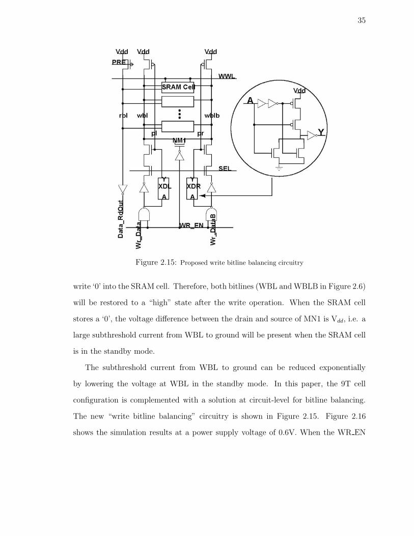
For comparative evaluation, a 1x128 SRAM cell array operating at power supply
voltage of 0.6V is used to assess the power dissipation of 6T and 9T cell arrays in
standby mode. All the simulation results are obtained by using Berkeley Predictive
Technology Model at 32nm [52]. The transistor sizes of the 6T and 9T SRAM cell
are the same. As shown in Table 2.2, the 9T SRAM array with the proposed write
bitline balancing circuit achieves a significant power reduction at the three different
process corners, i.e. power savings of 33%, 20%, and 29% at typical, fast, and slow
corners, respectively. Therefore, the subthreshold leakage is reduced both at cell-level
and at array-level (by using the novel balancing circuitry as proposed in the previous
section).
37
Figure 2.16: Simulation results for the write operation of the proposed 9T SRAM array
2.4 A Metric for Memory Cells
To compare the different memory cell configurations found in the technical literature
with the 9T cell of this paper, a novel metric is introduced in this section. This is
required to comprehensively assess the performance (as a function of the delay), sta-
bility (with respect to noise) and power dissipation within a single yet comprehensive
metric that relies on the simulation results of the previous sections.
It has been shown in [22] that SNM and SINMmust be both used when considering
the static stability of a SRAM cell. Therefore, SNM and SINM can be multiplied
together, thus yielding a comprehensive figure of merit as the Static Power Noise
38
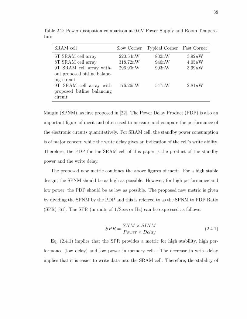
Table 2.2: Power dissipation comparison at 0.6V Power Supply and Room Tempera-ture
SRAM cell Slow Corner Typical Corner Fast Corner
6T SRAM cell array 220.54nW 832nW 3.92μW8T SRAM cell array 318.72nW 946nW 4.05μW9T SRAM cell array with-out proposed bitline balanc-ing circuit
296.90nW 903nW 3.99μW
9T SRAM cell array withproposed bitline balancingcircuit
176.26nW 547nW 2.81μW
Margin (SPNM), as first proposed in [22]. The Power Delay Product (PDP) is also an
important figure of merit and often used to measure and compare the performance of
the electronic circuits quantitatively. For SRAM cell, the standby power consumption
is of major concern while the write delay gives an indication of the cell’s write ability.
Therefore, the PDP for the SRAM cell of this paper is the product of the standby
power and the write delay.
The proposed new metric combines the above figures of merit. For a high stable
design, the SPNM should be as high as possible. However, for high performance and
low power, the PDP should be as low as possible. The proposed new metric is given
by dividing the SPNM by the PDP and this is referred to as the SPNM to PDP Ratio
(SPR) [61]. The SPR (in units of 1/Secs or Hz) can be expressed as follows:
SPR =SNM × SINM
Power ×Delay(2.4.1)
Eq. (2.4.1) implies that the SPR provides a metric for high stability, high per-
formance (low delay) and low power in memory cells. The decrease in write delay
implies that it is easier to write data into the SRAM cell. Therefore, the stability of
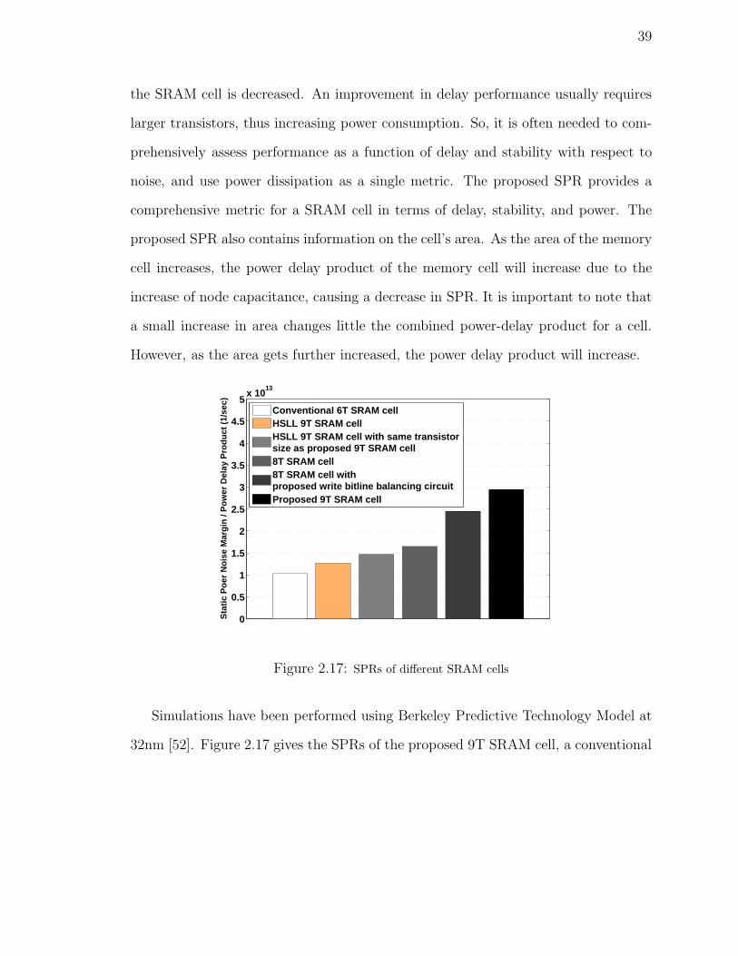
39
the SRAM cell is decreased. An improvement in delay performance usually requires
larger transistors, thus increasing power consumption. So, it is often needed to com-
prehensively assess performance as a function of delay and stability with respect to
noise, and use power dissipation as a single metric. The proposed SPR provides a
comprehensive metric for a SRAM cell in terms of delay, stability, and power. The
proposed SPR also contains information on the cell’s area. As the area of the memory
cell increases, the power delay product of the memory cell will increase due to the
increase of node capacitance, causing a decrease in SPR. It is important to note that
a small increase in area changes little the combined power-delay product for a cell.
However, as the area gets further increased, the power delay product will increase.
0
0.5
1
1.5
2
2.5
3
3.5
4
4.5
5x 10
13
Sta
tic
Po
er N
ois
e M
arg
in /
Po
wer
Del
ay P
rod
uct
(1/
sec)
Conventional 6T SRAM cellHSLL 9T SRAM cellHSLL 9T SRAM cell with same transistorsize as proposed 9T SRAM cell8T SRAM cell8T SRAM cell withproposed write bitline balancing circuitProposed 9T SRAM cell
Figure 2.17: SPRs of different SRAM cells
Simulations have been performed using Berkeley Predictive Technology Model at
32nm [52]. Figure 2.17 gives the SPRs of the proposed 9T SRAM cell, a conventional
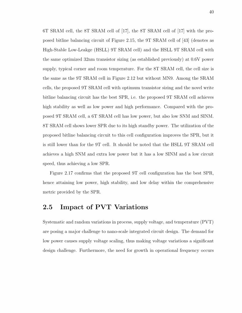
40
6T SRAM cell, the 8T SRAM cell of [17], the 8T SRAM cell of [17] with the pro-
posed bitline balancing circuit of Figure 2.15, the 9T SRAM cell of [43] (denotes as
High-Stable Low-Leakge (HSLL) 9T SRAM cell) and the HSLL 9T SRAM cell with
the same optimized 32nm transistor sizing (as established previously) at 0.6V power
supply, typical corner and room temperature. For the 8T SRAM cell, the cell size is
the same as the 9T SRAM cell in Figure 2.12 but without MN9. Among the SRAM
cells, the proposed 9T SRAM cell with optimum transistor sizing and the novel write
bitline balancing circuit has the best SPR, i.e. the proposed 9T SRAM cell achieves
high stability as well as low power and high performance. Compared with the pro-
posed 9T SRAM cell, a 6T SRAM cell has low power, but also low SNM and SINM.
8T SRAM cell shows lower SPR due to its high standby power. The utilization of the
proposed bitline balancing circuit to this cell configuration improves the SPR, but it
is still lower than for the 9T cell. It should be noted that the HSLL 9T SRAM cell
achieves a high SNM and extra low power but it has a low SINM and a low circuit
speed, thus achieving a low SPR.
Figure 2.17 confirms that the proposed 9T cell configuration has the best SPR,
hence attaining low power, high stability, and low delay within the comprehensive
metric provided by the SPR.
2.5 Impact of PVT Variations
Systematic and random variations in process, supply voltage, and temperature (PVT)
are posing a major challenge to nano-scale integrated circuit design. The demand for
low power causes supply voltage scaling, thus making voltage variations a significant
design challenge. Furthermore, the need for growth in operational frequency occurs

41
at high junction temperatures and within die temperature variations. Figure 2.18
shows the static power and write delay product for the proposed 9T SRAM cell
using the write circuitry in Figure 2.15 and the conventional 6T SRAM cell design of
[16] with inter-die variations. Simulation results show that the 9T SRAM cell has a
lower power delay product as well as less sensitivity due to power and temperature
variations because the proposed 9T SRAM cell and bitline balancing scheme reduce
the leakage power up to 33% without degrading the speed of the memory cell. With
the bitline balancing scheme, the subthreshold leakage of the 9T SRAM cell array is
significantly reduced. The subthreshold leakage component takes a significant portion
of the total power; therefore, the power delay product variation of the 9T SRAM cell
is also reduced since the subthreshold leakage is very sensitive to temperature and
voltage change.
As CMOS technology scales down into the nano ranges, process variations are
a serious concern due to uncertainty in the device and interconnects characteristics.
Process variations negatively impact the speed, stability, and power consumption of
traditional SRAM designs [11]. In this section, the stability of SRAM cells is evaluated
in the presence of process variations, i.e. intra-die variation and local mismatches,
in the channel length and the threshold voltage of the transistors. Figure 2.19 and
Figure 2.20 show the power-delay product of the 6T SRAM cell and the 9T SRAM cell
with variations in mobility, threshold voltage, and velocity saturation, respectively.
Figure 2.21 shows the power-delay product of the 6T SRAM cell and the 9T SRAM
cell with variations in channel length. At 32nm feature size, channel length and
threshold voltage variations have the most significant impact on cell performance
while mobility and velocity saturation have the least impact. Monte Carlo analysis on

42
Figure 2.18: Power-delay product of the SRAM cells at different temperatures and power suppliesfor a) proposed 9T cell; b) 6T cell
the stability of the SRAM cells shows that the 6T cell could fail at 0.6V power supply,
typical corner, and room temperature in the presence of process variations while the
9T cell has SNM of 240mV and SINM of 23.61μA at the worst case. Therefore, the
9T cell achieves excellent stability in the presence of process variations.
The impact of the threshold voltage variations, i.e., process variations, on the
power consumption of the individual SRAM cell has been assessed by Monte Carlo
analysis. The threshold voltage distribution is modeled as a ± 5% Gaussian with
variation of threshold voltage at a ± 3-sigma level. Simulation results are shown in
Figure 2.22, where the power consumption of the 6T SRAM cell decreases as the
average threshold voltage increases. In the 9T SRAM cell, the power consumption
variation caused by the variation in the threshold voltage is significantly smaller than
43
Saturation VelocityThreshold Voltage Mobility0
0.5
1
1.5
2
2.5
3
3.5x 10
−19
Po
wer
Del
ay P
rod
uct
(J)
Variation of −10%Nominal ValueVariation of +10%
Figure 2.19: Power-delay product of the SRAM cells with the variations of mobility, thresholdvoltage, and velocity saturation for proposed 9T cell
for the 6T SRAM cell case because the subthreshold leakage current is significantly
reduced. Figure 2.23 shows the distribution of the power delay product due to process
variations, i.e. intra-die variation and local mismatches, including transistor geometry
variations, threshold variation, and mobility variation. Unlike the power consumption
Monte Carlo analysis due to process variation, more parameters need to be modeled
for more accurate power delay product Monte Carlo analysis. Parameter variations
are modeled using a ± 5% Gaussian distribution with variations at a ± 3-sigma level
for all the parameters. All power delay product results are normalized with respect to
the arithmetic mean of the power delay product of the proposed 9T SRAM cell. As
shown in Figure 2.23, the power delay product variance of the proposed 9T SRAM
cell is also lower compared to the distribution of the 6T SRAM cell. While the bitline
voltage is reduced during standby mode by using the balancing circuit of Figure 2.15,
very low power consumption and a considerable mitigation of the impact of process
variations are accomplished by using the design method for the 9T SRAM cell.
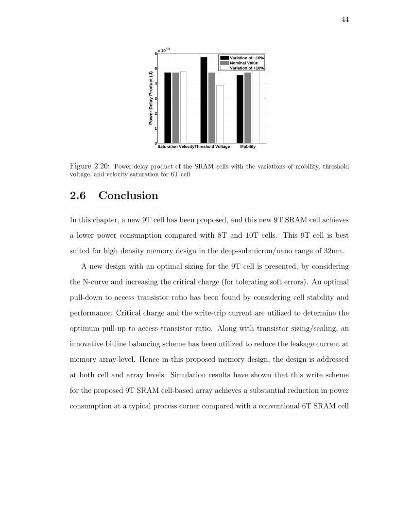
44
Saturation VelocityThreshold Voltage Mobility0
1
2
3
4
5
6x 10
−19
Po
wer
Del
ay P
rod
uct
(J)
Variation of −10%Nominal ValueVariation of +10%
Figure 2.20: Power-delay product of the SRAM cells with the variations of mobility, thresholdvoltage, and velocity saturation for 6T cell
2.6 Conclusion
In this chapter, a new 9T cell has been proposed, and this new 9T SRAM cell achieves
a lower power consumption compared with 8T and 10T cells. This 9T cell is best
suited for high density memory design in the deep-submicron/nano range of 32nm.
A new design with an optimal sizing for the 9T cell is presented, by considering
the N-curve and increasing the critical charge (for tolerating soft errors). An optimal
pull-down to access transistor ratio has been found by considering cell stability and
performance. Critical charge and the write-trip current are utilized to determine the
optimum pull-up to access transistor ratio. Along with transistor sizing/scaling, an
innovative bitline balancing scheme has been utilized to reduce the leakage current at
memory array-level. Hence in this proposed memory design, the design is addressed
at both cell and array levels. Simulation results have shown that this write scheme
for the proposed 9T SRAM cell-based array achieves a substantial reduction in power
consumption at a typical process corner compared with a conventional 6T SRAM cell
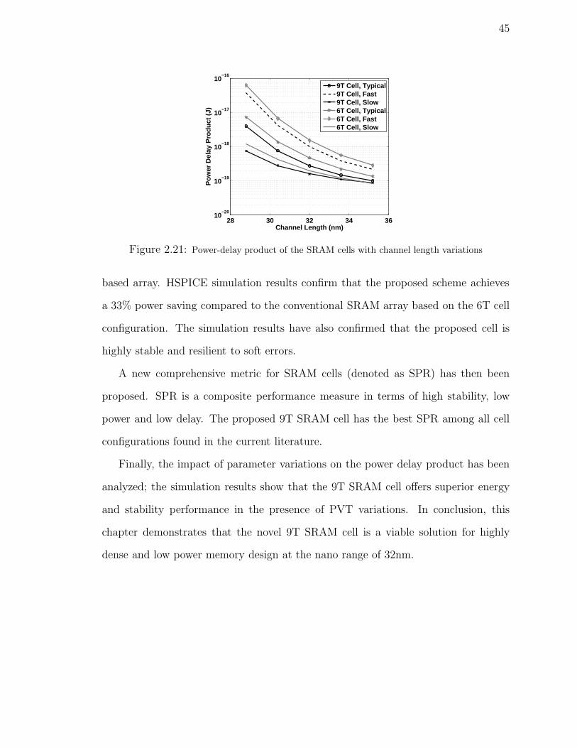
45
28 30 32 34 3610
−20
10−19
10−18
10−17
10−16
Channel Length (nm)
Po
wer
Del
ay P
rod
uct
(J)
9T Cell, Typical9T Cell, Fast9T Cell, Slow6T Cell, Typical6T Cell, Fast6T Cell, Slow
Figure 2.21: Power-delay product of the SRAM cells with channel length variations
based array. HSPICE simulation results confirm that the proposed scheme achieves
a 33% power saving compared to the conventional SRAM array based on the 6T cell
configuration. The simulation results have also confirmed that the proposed cell is
highly stable and resilient to soft errors.
A new comprehensive metric for SRAM cells (denoted as SPR) has then been
proposed. SPR is a composite performance measure in terms of high stability, low
power and low delay. The proposed 9T SRAM cell has the best SPR among all cell
configurations found in the current literature.
Finally, the impact of parameter variations on the power delay product has been
analyzed; the simulation results show that the 9T SRAM cell offers superior energy
and stability performance in the presence of PVT variations. In conclusion, this
chapter demonstrates that the novel 9T SRAM cell is a viable solution for highly
dense and low power memory design at the nano range of 32nm.
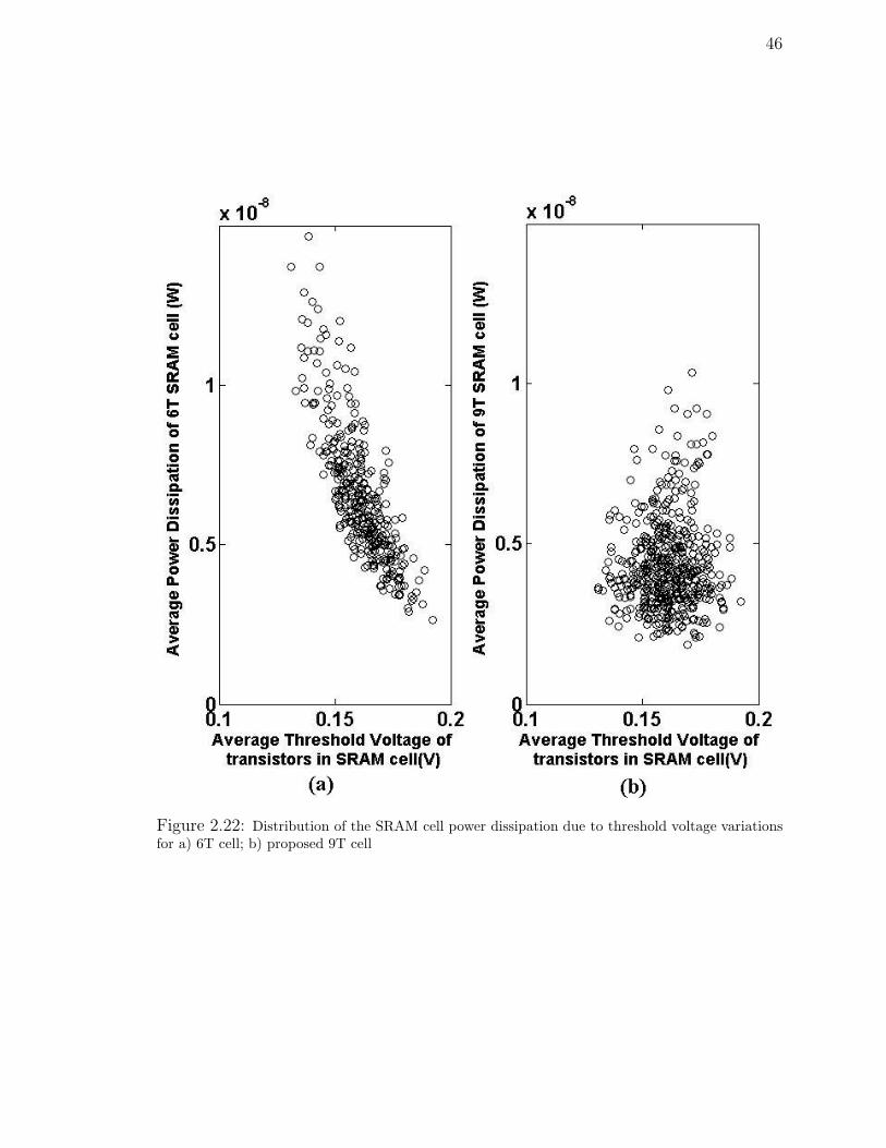
46
Figure 2.22: Distribution of the SRAM cell power dissipation due to threshold voltage variationsfor a) 6T cell; b) proposed 9T cell

47
0 1 2 3 40
1000
2000
Normalized Power−Delay Product of 9T SRAM cell
Occ
urr
ence
s
0 1 2 3 40
1000
2000
Normalized Power−Delay Product of 6T SRAM cell
Occ
urr
ence
s
Figure 2.23: Power-delay product distributions of the 6T and the proposed 9T cell due to processvariations

Chapter 3
Analysis and Design of CNTFETSRAM Cell for Low Leakage andHigh Stability
3.1 Introduction
At nano feature sizes, scaling has resulted in increased short-channel effects, reduced
gate control, exponentially rising leakage currents, severe process variations, and high
power density. As today’s VLSI systems mostly rely on silicon MOS technology, the
Industry Technology Roadmap (ITR) has predicted that in the nano regimes, the
expected high density will encounter substantial difficulties in terms of physical phe-
nomena and technology limitations, possibly preventing the continued improvements
in figures of merit such as low power and high reliability. Nanoscaled alternatives to
bulk silicon transistors are therefore being pursued. Ultra thin body devices such as
FinFETs have received an increasing attention in recent years [69]. Furthermore, new
materials and devices have been investigated to replace silicon in nanoscaled transis-
tors from the year 2015 and beyond (as per ITR prediction). Carbon nanotube tran-
sistors (CNTFETs), for example, are promising due to their unique one-dimensional
48
49
band-structure that suppresses backscattering and makes near-ballistic operation a
realistic possibility [55] [2] [25] [42].
Design of fast and power efficient memory structures continues to be of the high-
est priority, and ballistic transport operation and low off current make the CNTFET
a suitable device for high performance and increased integration density of SRAM
design. Moreover, the MOSFET-like model of the CNTFET is likely to be scalable
down to 10nm channel length, thus providing a substantial performance and power
improvement compared to the MOSFET model (with minimum channel length of
32nm [74]). Therefore, a SRAM design implemented using CNTFETs requires a sig-
nificantly smaller area than its CMOS counterpart. A resistive-load CNTFET-based
SRAM cell has been proposed in [6]. However, large off-chip resistors (i.e. 100MΩ) are
needed in the configuration due to the current requirements of the CNTFETs. This
resistive-load CNTFET-based SRAM cell design is modified with P-type transistors
as active load to address this problem as proposed in this chapter.
The use of transistors with multiple threshold voltages (i.e. a so-called multi-
threshold design) is widely utilized in today’s CMOS circuits to improve performance.
The threshold voltage can be changed by applying different bias voltages to the bulk
terminal of the CMOS transistors. The threshold voltage of CNTFET is determined
by the CNT diameter. Therefore, CNTFETs with different threshold voltages can be
accomplished by growing CNTs with different diameters (chiralities).
In this chapter, a CNTFET-based SRAM cell design with optimized threshold
voltages is proposed, assessed, and compared to the CMOS implementation of the
same cell. Different diameters (and therefore chirality) are utilized for the two types
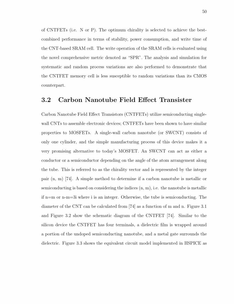
50
of CNTFETs (i.e. N or P). The optimum chirality is selected to achieve the best-
combined performance in terms of stability, power consumption, and write time of
the CNT-based SRAM cell. The write operation of the SRAM cells is evaluated using
the novel comprehensive metric denoted as “SPR”. The analysis and simulation for
systematic and random process variations are also performed to demonstrate that
the CNTFET memory cell is less susceptible to random variations than its CMOS
counterpart.
3.2 Carbon Nanotube Field Effect Transister
Carbon Nanotube Field Effect Transistors (CNTFETs) utilize semiconducting single-
wall CNTs to assemble electronic devices; CNTFETs have been shown to have similar
properties to MOSFETs. A single-wall carbon nanotube (or SWCNT) consists of
only one cylinder, and the simple manufacturing process of this device makes it a
very promising alternative to today’s MOSFET. An SWCNT can act as either a
conductor or a semiconductor depending on the angle of the atom arrangement along
the tube. This is referred to as the chirality vector and is represented by the integer
pair (n, m) [74]. A simple method to determine if a carbon nanotube is metallic or
semiconducting is based on considering the indices (n, m), i.e. the nanotube is metallic
if n=m or n-m=3i where i is an integer. Otherwise, the tube is semiconducting. The
diameter of the CNT can be calculated from [74] as a function of m and n. Figure 3.1
and Figure 3.2 show the schematic diagram of the CNTFET [74]. Similar to the
silicon device the CNTFET has four terminals, a dielectric film is wrapped around
a portion of the undoped semiconducting nanotube, and a metal gate surrounds the
dielectric. Figure 3.3 shows the equivalent circuit model implemented in HSPICE as

51
proposed in [74]. Heavily doped CNT segments are placed between the gate and the
source/drain to allow for a low series resistance during the on-state [5]. As the gate
potential increases, the device is electrostatically turned on or off via the gate.
The current-voltage (I-V) characteristics of the CNTFET are shown in Figure 3.4,
and they are similar to those of MOSFET. The CNTFET device current is saturated
at higher Vds (drain to source voltage) as channel length increases as shown in Fig-
ure 3.4, and the on-current decreases due to energy quantization in the axial direction
at 32nm (or less) gate length [74]. The threshold voltage is defined as the voltage
required to turn on the transistor, and the threshold voltage of the intrinsic CNT
channel can be approximated to the first order as the half bandgap which is an in-
verse function of the diameter [74]:
Vth ≈ Eg
2e=
√3
3
α× Vπ
e×DCNT
(3.2.1)
where α = 2.49 Ais the carbon to carbon atom distance, Vπ = 3.033 eV is the
carbon π-π bond energy in the tight bonding model, e is the unit electron charge,
and DCNT is the CNT diameter. Then, the threshold voltage of the CNTFETs using
(19, 0) CNTs as channels is 0.289V because the DCNT of a (19, 0) CNT is 1.49nm.
Simulation results have confirmed the correctness of this threshold voltage. As the
chirality vector changes, the threshold voltage of the CNTFET will also change. The
threshold voltage of the CNTFET is inversely proportional to the chirality vector of
the CNT. For example, the threshold voltage of the CNTFET using (13, 0) CNTs
is 0.423V, while the threshold voltage of the CNTFET using (19, 0) is 0.289V. Fig-
ure 3.5 shows the threshold voltage of P-type CNTFET (PCNTFET) with CNTs of
different chirality vectors. For N-type CNTFET (NCNTFET), the threshold voltage
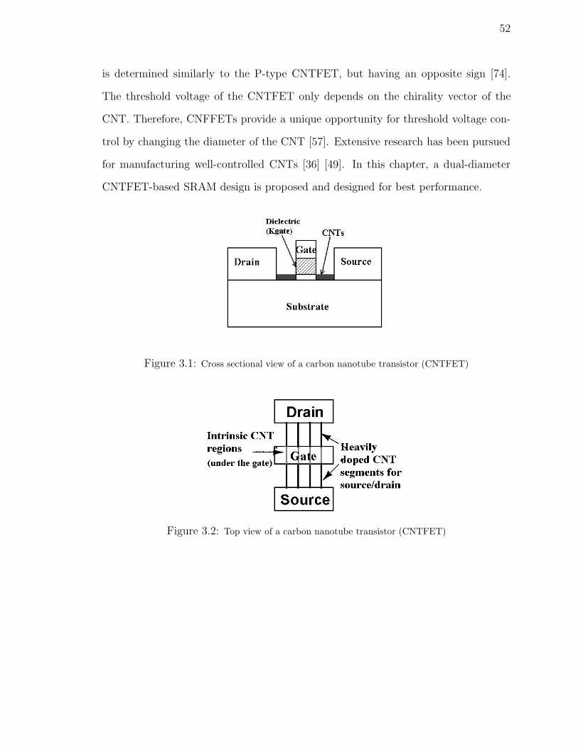
52
is determined similarly to the P-type CNTFET, but having an opposite sign [74].
The threshold voltage of the CNTFET only depends on the chirality vector of the
CNT. Therefore, CNFFETs provide a unique opportunity for threshold voltage con-
trol by changing the diameter of the CNT [57]. Extensive research has been pursued
for manufacturing well-controlled CNTs [36] [49]. In this chapter, a dual-diameter
CNTFET-based SRAM design is proposed and designed for best performance.
Figure 3.1: Cross sectional view of a carbon nanotube transistor (CNTFET)
Figure 3.2: Top view of a carbon nanotube transistor (CNTFET)
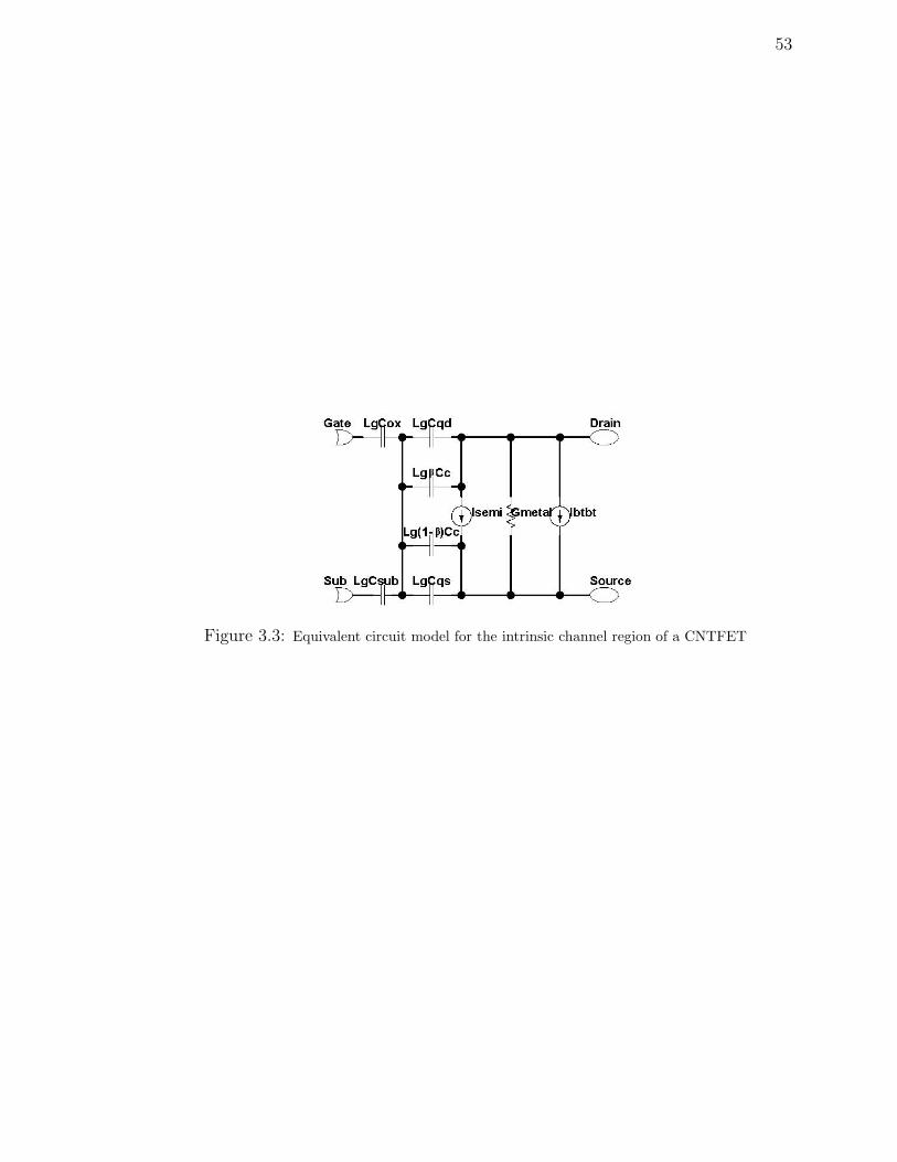
53
Figure 3.3: Equivalent circuit model for the intrinsic channel region of a CNTFET

54
Figure 3.4: Current-voltage (I-V) characteristics of a ballistic CNTFET

55
Figure 3.5: Threshold voltage of P-type CNTFET with different chirality vectors
3.3 Design of 6T SRAM using CNTFET
Figure 3.6 shows the conventional six-transistor (6T) SRAM cell configuration used
as the core storage element of most register file and cache designs in CMOS. With
today’s aggressive scaling, substantial problems such as power consumption and sta-
bility have already been encountered when the 6T SRAM cell configuration is utilized
in CMOS at nanoscale ranges. In this chapter, the 6T SRAM cell of Figure 3.6 is
designed using CNTFETs (shown in Figure 3.7) and its performance is assessed com-
prehensively with a newly proposed figure of merit denotes as “SPR” to compare
stability, power dissipation, and write time with other existing SRAM cell designs.
The basic design concept of the CNTFET-based memory has been proposed in [39]
previously, and this chapter presents the actual design of the concept addressing
the realistic design challenges and issues such as performance, Static Noise Margin
(SNM), power consumption, and tolerance to PVT variations.
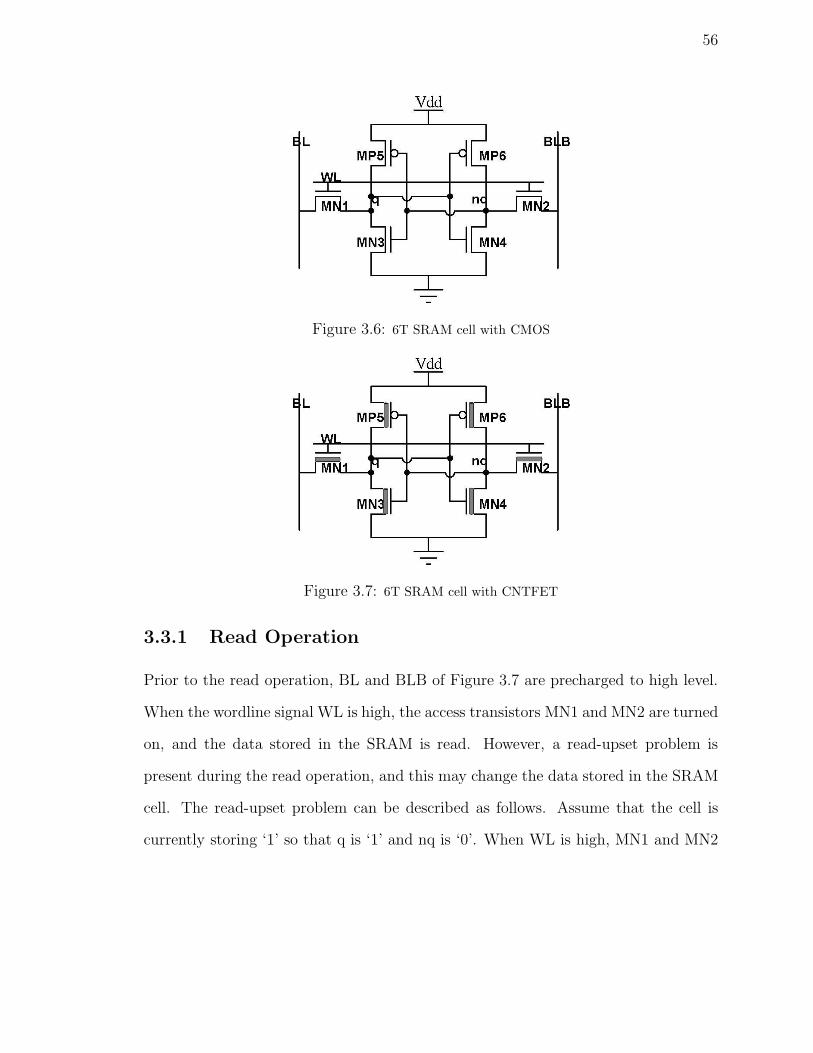
56
Figure 3.6: 6T SRAM cell with CMOS
Figure 3.7: 6T SRAM cell with CNTFET
3.3.1 Read Operation
Prior to the read operation, BL and BLB of Figure 3.7 are precharged to high level.
When the wordline signal WL is high, the access transistors MN1 and MN2 are turned
on, and the data stored in the SRAM is read. However, a read-upset problem is
present during the read operation, and this may change the data stored in the SRAM
cell. The read-upset problem can be described as follows. Assume that the cell is
currently storing ‘1’ so that q is ‘1’ and nq is ‘0’. When WL is high, MN1 and MN2
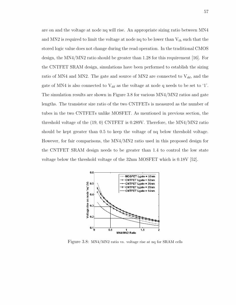
57
are on and the voltage at node nq will rise. An appropriate sizing ratio between MN4
and MN2 is required to limit the voltage at node nq to be lower than Vth such that the
stored logic value does not change during the read operation. In the traditional CMOS
design, the MN4/MN2 ratio should be greater than 1.28 for this requirement [16]. For
the CNTFET SRAM design, simulations have been performed to establish the sizing
ratio of MN4 and MN2. The gate and source of MN2 are connected to Vdd, and the
gate of MN4 is also connected to Vdd as the voltage at node q needs to be set to ‘1’.
The simulation results are shown in Figure 3.8 for various MN4/MN2 ratios and gate
lengths. The transistor size ratio of the two CNTFETs is measured as the number of
tubes in the two CNTFETs unlike MOSFET. As mentioned in previous section, the
threshold voltage of the (19, 0) CNTFET is 0.289V. Therefore, the MN4/MN2 ratio
should be kept greater than 0.5 to keep the voltage of nq below threshold voltage.
However, for fair comparisons, the MN4/MN2 ratio used in this proposed design for
the CNTFET SRAM design needs to be greater than 1.4 to control the low state
voltage below the threshold voltage of the 32nm MOSFET which is 0.18V [52].
Figure 3.8: MN4/MN2 ratio vs. voltage rise at nq for SRAM cells

58
3.3.2 Write Operation
During the write operation, the wordline WL is high to allow the data on bitlines
BL and BLB to be written into the SRAM cell. For a successful write to a SRAM
cell, the pull up transistor should not be too strong. Assume that the SRAM cell is
storing ‘1’ and it is required to write a new data ‘0’ into the SRAM cell. The node
q in Figure 3.7 is going to be low, so the pass gate MN1 must be significantly more
conductive than the PMOS MP5. In the traditional CMOS design, the MP5/MN1
ratio should not be greater than 1.6 [16]. For CNTFET SRAM design, simulations
have been performed to establish the size ratio between MP5 and MN1. The bias
voltage on the gate of MP5 is kept below Vth, and the bias voltage on the gate of
MN1 is Vdd. Figure 3.9 shows the simulation results for various ratios and channel
lengths. Any MP5/MN1 ratio of less than 1.6 can pull node q below 0.289 V, which
is the threshold voltage of a CNTFET with (19, 0) nanotubes. Similarly to the read
operation, the MP5/MN1 ratio used in this proposed design for the CNTFET SRAM
design needs to be less than 1 to ensure that the write voltage at node q is not higher
than the threshold voltage of the 32nm MOSFET (i.e. 0.18V).
Therefore, for the proposed dual-diameter CNTFET-based SRAM cell design, the
transistor size ratios among the pull up FET, the pull down FET, and the access
transistors are MP5/MN1 = 0.5 and MN4/MN2 = 1.5. P-type CNTFETs with one
tube are used for MP5 and MP6, while n-type CNTFETs with three tubes are used
for MN3 and MN4. The number of tubes used for MN1 and MN2 is two. As the
channel length of the CNTFET decreases to 32nm or below, the drain current of
the CNTFET decreases due to energy quantization in the axial direction. Phonon
scattering in short-channel devices further reduces the on-current [18]. As shown in
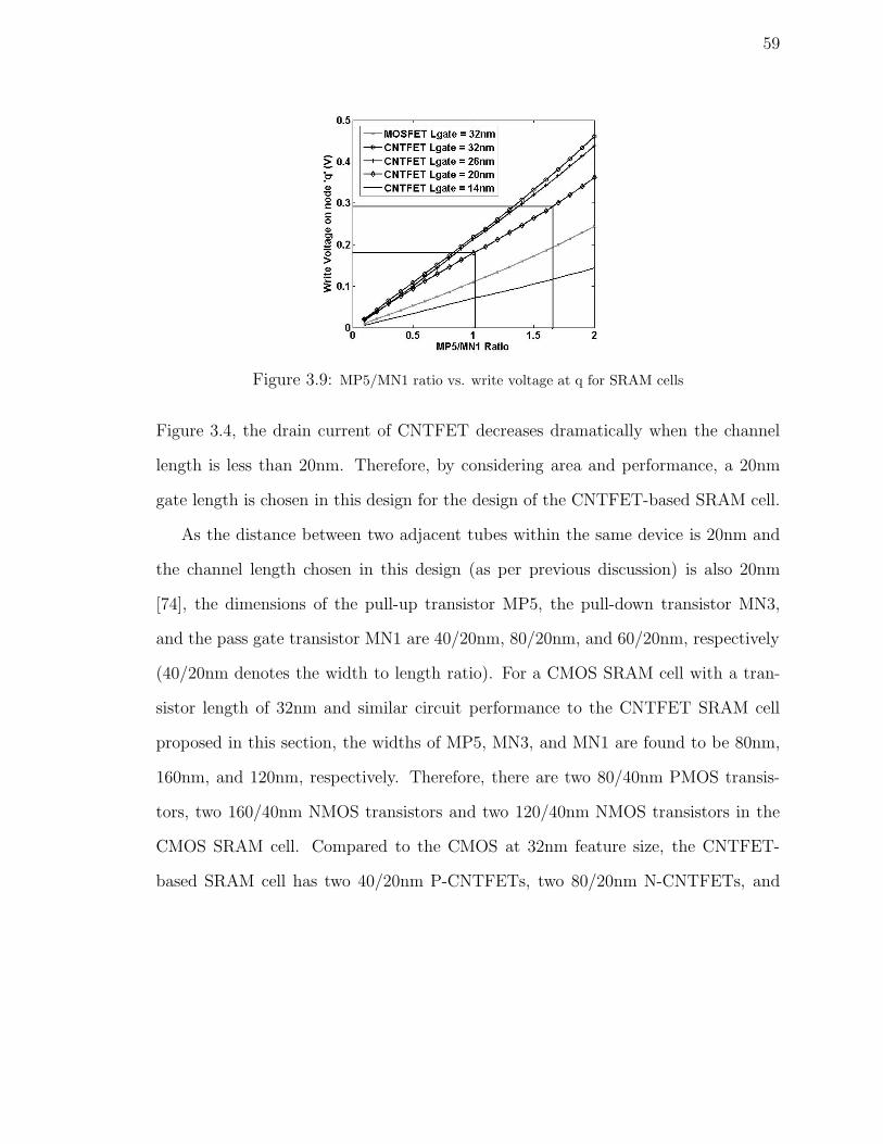
59
Figure 3.9: MP5/MN1 ratio vs. write voltage at q for SRAM cells
Figure 3.4, the drain current of CNTFET decreases dramatically when the channel
length is less than 20nm. Therefore, by considering area and performance, a 20nm
gate length is chosen in this design for the design of the CNTFET-based SRAM cell.
As the distance between two adjacent tubes within the same device is 20nm and
the channel length chosen in this design (as per previous discussion) is also 20nm
[74], the dimensions of the pull-up transistor MP5, the pull-down transistor MN3,
and the pass gate transistor MN1 are 40/20nm, 80/20nm, and 60/20nm, respectively
(40/20nm denotes the width to length ratio). For a CMOS SRAM cell with a tran-
sistor length of 32nm and similar circuit performance to the CNTFET SRAM cell
proposed in this section, the widths of MP5, MN3, and MN1 are found to be 80nm,
160nm, and 120nm, respectively. Therefore, there are two 80/40nm PMOS transis-
tors, two 160/40nm NMOS transistors and two 120/40nm NMOS transistors in the
CMOS SRAM cell. Compared to the CMOS at 32nm feature size, the CNTFET-
based SRAM cell has two 40/20nm P-CNTFETs, two 80/20nm N-CNTFETs, and
60
two 60/20nm N-CNTFETs. These transistors are used in the next section to estab-
lish the best operation under the optimized threshold voltages for the dual-diameter
CNTFET-based SRAM cell.
3.4 Dual-Chirality SRAM Cell Design
Since the threshold voltage of CNTFET can be controlled by adjusting tube’s diame-
ter, the design of CNTFET-based circuits with different threshold voltages is possible
because CNTs can be grown with different diameters [57] [36] [49]. In this proposed
SRAM design, N-type and P-type CNTFETs use CNTs that have different chirality
vectors for the best (optimized) performance. However, all N-type CNTFETs use
CNTs with the same chirality vector and all P-type CNTFETs use the same chirality
vector as well (the dual-diameter arrangement is used for simplicity, although addi-
tional threshold voltages could also be utilized by using CNTs different diameters in
the transistors).
A new index is defined for the CNTFET-based SRAM design, and it is given by
the triplet (np, nn, m), where np and nn represent the first chirality vector “n” of
the PCNTFETs and NCNTFETs, respectively, and m is the common second chirality
vector “m” of the two CNTFETs. For example, a SRAM cell with (16, 0) PCNTFETs
and (19, 0) NCNTFETs is represented by the index triplet (16, 19, 0). The difference
in chirality between N-type and P-type CNTFETs must also take into account the
performance of the SRAMmemory cell. As for CMOS SRAM, the threshold voltage of
the pull-up P-type FETs (MP5 and MP6 shown in Figure 3.7) have a close relationship
with the Static Noise Margin (SNM) of the SRAM cell (the SNM is defined as the
maximum value of DC noise voltage that can be tolerated by the SRAM cell without

61
changing the stored bit [64]). The SNM is commonly used as a metric for static
stability of a SRAM cell [22].
To investigate the SNM of the proposed dual-diameter CNTFET SRAM, extensive
simulations have been performed on CNTFET SRAM cells with index triplets of
(10, 19, 0), (13, 19, 0), (16, 19, 0), (19, 19, 0), and (22, 19, 0) for the transistors.
Figure 3.10 and Figure 3.11 show the simulation results of the read SNM of the
SRAM cell at 0.9V power supply and room temperature. For the 6T SRAM cell
configuration in Figure 3.6 and Figure 3.7, the worst-case stability condition occurs
when the cell is accessed for read operation, i.e. the read SNM is lower than the hold
SNM. Simulation has shown that as the chirality vector of the PCNTFETs changes
from (10, 0) to (22, 0), then the SNM of the CNTFET SRAM is increased. As shown
in Figure 3.10, the read SNM of the CNTFET SRAM is larger than for the CMOS
SRAM at 32nm feature size. Simulation has also been performed by changing the
chirality vector of the N-type CNTFETs in the range from (10, 0) to (22, 0). As
shown in Figure 3.11, the values of the read SNM of the CNTFET SRAM change
little as the chirality vectors of the N-type CNTFETs change. Therefore, for best
stability, the chirality vector of the PCNTFETs must be adjusted.
The stability of the SRAM cell can be increased by decreasing the absolute value
of the threshold voltage of the pull-up transistor by controlling its chirality vector.
However, there is a conflicting constraint between performance and stability. At a
better ability to hold data, it is also harder to write new data into the SRAM cell,
i.e. it takes more time to write new data. To find the optimum chirality for both
PCNTFETs and NCNTFETs, both the SNM and the write time must be considered.
Table 3.1 shows the SNM and the write time of the CNTFET SRAM cell with different

62
Figure 3.10: Static Noise Margin (SNM) of the SRAM cell with different PCNTFET chiralityvectors
threshold voltages of the PCNTFET at 0.9V power supply and room temperature.
Both the SNM and the write time increase with decrease of the absolute value of the
threshold voltage of the pull-up transistor. For a highly stable and low delay design,
a high SNM and a fast write time are desired. Therefore, the SNM is divided by
the write time to find the best threshold voltage of the PCNTFET for both high
SNM and fast write time. As shown in Table 3.1, when the threshold voltage of the
PCNTFET is |0.343V | for a (16, 19, 0) SRAM cell, the ratio between the SNM and
the write time is the highest among those CNTFET SRAM cells listed in Table 3.1.
Therefore, the (16, 19, 0) SRAM cell is selected for best overall performance. It is
also shown in Table 3.1 that the ratio between the SNM and the write time for the
CNTFET SRAM cell is significantly higher than for the CMOS SRAM cell, i.e. high
stability is attained at a low write time.
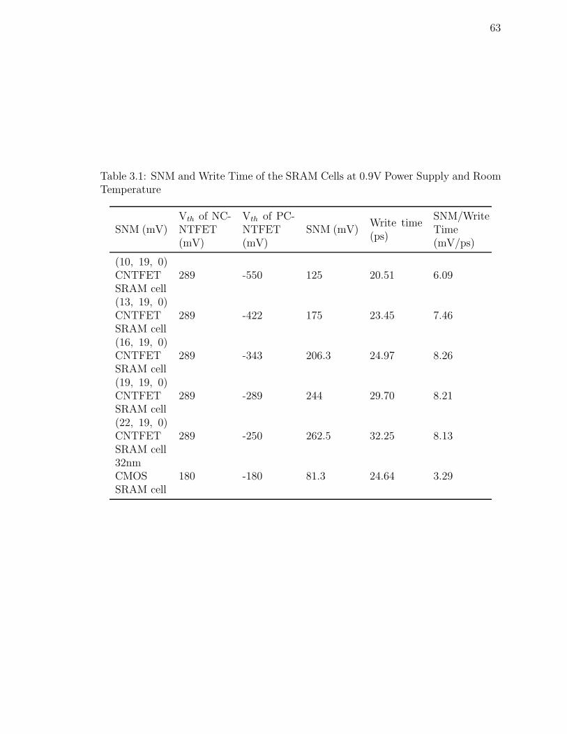
63
Table 3.1: SNM and Write Time of the SRAM Cells at 0.9V Power Supply and RoomTemperature
SNM (mV)Vth of NC-NTFET(mV)
Vth of PC-NTFET(mV)
SNM (mV)Write time(ps)
SNM/WriteTime(mV/ps)
(10, 19, 0)CNTFETSRAM cell
289 -550 125 20.51 6.09
(13, 19, 0)CNTFETSRAM cell
289 -422 175 23.45 7.46
(16, 19, 0)CNTFETSRAM cell
289 -343 206.3 24.97 8.26
(19, 19, 0)CNTFETSRAM cell
289 -289 244 29.70 8.21
(22, 19, 0)CNTFETSRAM cell
289 -250 262.5 32.25 8.13
32nmCMOSSRAM cell
180 -180 81.3 24.64 3.29

64
Figure 3.11: Static Noise Margin (SNM) of the SRAM cell with different NCNTFET chiralityvectors
3.5 A Metric for Memory Cells
To compare the dual-diameter CNTFET and CMOS SRAM cell configurations, a
metric, which has been introduced in Chapter 2, is utilized in this section,. This is
required to comprehensively assess the performance as a function of delay, stability
with respect to noise, and power dissipation within a comprehensive metric. HSPICE
simulations are performed using the Stanford CNTFET model [74] and the Berkeley
Predictive 32nm CMOS model [52] to compare the CNTFET and CMOS 6T SRAM
cells. It has been shown in [22] that both the Static Noise Margin (SNM) and the
Static Current Noise Margin (SINM) must be used to address the static stability of
a SRAM cell. Therefore, SNM and SINM are multiplied together to yield a com-
prehensive figure of merit as the Static Power Noise Margin (SPNM). The Power
Delay Product (PDP) is also an important figure of merit and often used to measure
and compare the circuits. It has been shown in articles [18] [30] that the CNTFET
has very high on/off current ratio compared with its CMOS counterpart. Therefore,
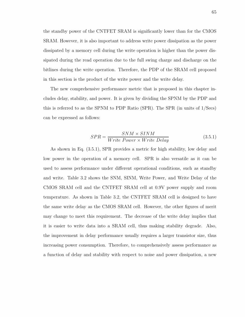
65
the standby power of the CNTFET SRAM is significantly lower than for the CMOS
SRAM. However, it is also important to address write power dissipation as the power
dissipated by a memory cell during the write operation is higher than the power dis-
sipated during the read operation due to the full swing charge and discharge on the
bitlines during the write operation. Therefore, the PDP of the SRAM cell proposed
in this section is the product of the write power and the write delay.
The new comprehensive performance metric that is proposed in this chapter in-
cludes delay, stability, and power. It is given by dividing the SPNM by the PDP and
this is referred to as the SPNM to PDP Ratio (SPR). The SPR (in units of 1/Secs)
can be expressed as follows:
SPR =SNM × SINM
Write Power ×Write Delay(3.5.1)
As shown in Eq. (3.5.1), SPR provides a metric for high stability, low delay and
low power in the operation of a memory cell. SPR is also versatile as it can be
used to assess performance under different operational conditions, such as standby
and write. Table 3.2 shows the SNM, SINM, Write Power, and Write Delay of the
CMOS SRAM cell and the CNTFET SRAM cell at 0.9V power supply and room
temperature. As shown in Table 3.2, the CNTFET SRAM cell is designed to have
the same write delay as the CMOS SRAM cell. However, the other figures of merit
may change to meet this requirement. The decrease of the write delay implies that
it is easier to write data into a SRAM cell, thus making stability degrade. Also,
the improvement in delay performance usually requires a larger transistor size, thus
increasing power consumption. Therefore, to comprehensively assess performance as
a function of delay and stability with respect to noise and power dissipation, a new
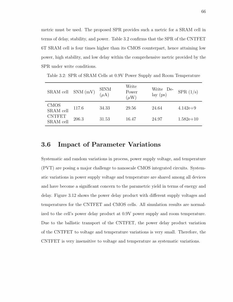
66
metric must be used. The proposed SPR provides such a metric for a SRAM cell in
terms of delay, stability, and power. Table 3.2 confirms that the SPR of the CNTFET
6T SRAM cell is four times higher than its CMOS counterpart, hence attaining low
power, high stability, and low delay within the comprehensive metric provided by the
SPR under write conditions.
Table 3.2: SPR of SRAM Cells at 0.9V Power Supply and Room Temperature
SRAM cell SNM (mV)SINM(μA)
WritePower(μW)
Write De-lay (ps)
SPR (1/s)
CMOSSRAM cell
117.6 34.33 29.56 24.64 4.142e+9
CNTFETSRAM cell
206.3 31.53 16.47 24.97 1.582e+10
3.6 Impact of Parameter Variations
Systematic and random variations in process, power supply voltage, and temperature
(PVT) are posing a major challenge to nanoscale CMOS integrated circuits. System-
atic variations in power supply voltage and temperature are shared among all devices
and have become a significant concern to the parametric yield in terms of energy and
delay. Figure 3.12 shows the power delay product with different supply voltages and
temperatures for the CNTFET and CMOS cells. All simulation results are normal-
ized to the cell’s power delay product at 0.9V power supply and room temperature.
Due to the ballistic transport of the CNTFET, the power delay product variation
of the CNTFET to voltage and temperature variations is very small. Therefore, the
CNTFET is very insensitive to voltage and temperature as systematic variations.
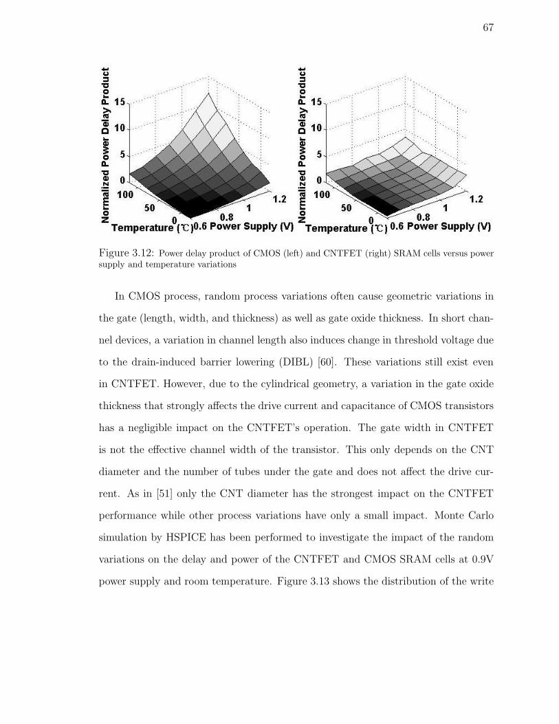
67
Figure 3.12: Power delay product of CMOS (left) and CNTFET (right) SRAM cells versus powersupply and temperature variations
In CMOS process, random process variations often cause geometric variations in
the gate (length, width, and thickness) as well as gate oxide thickness. In short chan-
nel devices, a variation in channel length also induces change in threshold voltage due
to the drain-induced barrier lowering (DIBL) [60]. These variations still exist even
in CNTFET. However, due to the cylindrical geometry, a variation in the gate oxide
thickness that strongly affects the drive current and capacitance of CMOS transistors
has a negligible impact on the CNTFET’s operation. The gate width in CNTFET
is not the effective channel width of the transistor. This only depends on the CNT
diameter and the number of tubes under the gate and does not affect the drive cur-
rent. As in [51] only the CNT diameter has the strongest impact on the CNTFET
performance while other process variations have only a small impact. Monte Carlo
simulation by HSPICE has been performed to investigate the impact of the random
variations on the delay and power of the CNTFET and CMOS SRAM cells at 0.9V
power supply and room temperature. Figure 3.13 shows the distribution of the write
68
time of the CNTFET and CMOS 6T SRAM cells under geometric parameters with
random changes. All simulation results are normalized to the SRAM’s write time
under no process variation. Figure 3.13 shows that the write time of the proposed
dual-diameter CNTFET 6T SRAM cell has much better tolerance to process varia-
tions compared to its CMOS counterpart. Figure 3.14 shows the distribution of the
standby power consumption of the CNTFET and CMOS 6T SRAM cells. Likewise
the previous cases, all simulated results are normalized to the SRAM cell standby
power consumption under no process variation. Due to the significantly low standby
power consumption and fewer parameters causing changes in power consumption, the
CNTFET SRAM cell shows a significantly better tolerance to process variations.
Figure 3.13: Write time distribution of CMOS and CNTFET SRAM cells
3.7 Conclusion
This chapter has investigated the use of CNTFETs in 6T SRAM design. As the
threshold voltage of the CNTFET can be easily controlled by changing the chirality
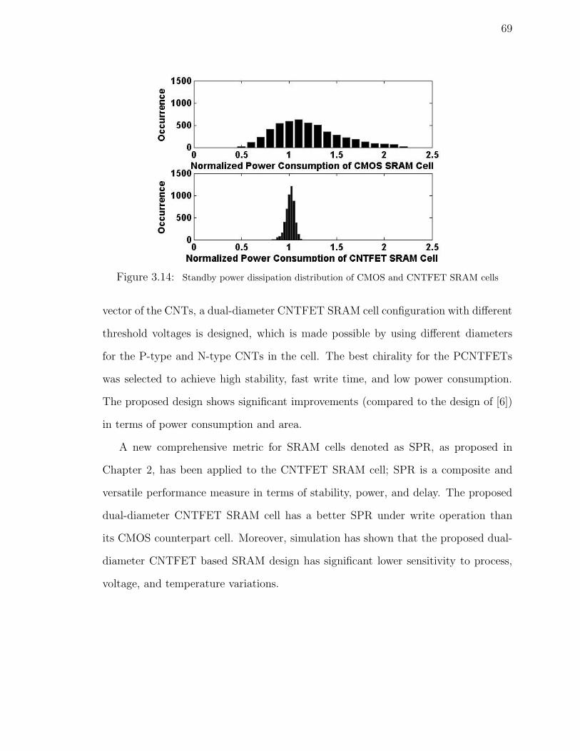
69
Figure 3.14: Standby power dissipation distribution of CMOS and CNTFET SRAM cells
vector of the CNTs, a dual-diameter CNTFET SRAM cell configuration with different
threshold voltages is designed, which is made possible by using different diameters
for the P-type and N-type CNTs in the cell. The best chirality for the PCNTFETs
was selected to achieve high stability, fast write time, and low power consumption.
The proposed design shows significant improvements (compared to the design of [6])
in terms of power consumption and area.
A new comprehensive metric for SRAM cells denoted as SPR, as proposed in
Chapter 2, has been applied to the CNTFET SRAM cell; SPR is a composite and
versatile performance measure in terms of stability, power, and delay. The proposed
dual-diameter CNTFET SRAM cell has a better SPR under write operation than
its CMOS counterpart cell. Moreover, simulation has shown that the proposed dual-
diameter CNTFET based SRAM design has significant lower sensitivity to process,
voltage, and temperature variations.
Chapter 4
Analysis and Design of Soft ErrorHardened Memory
4.1 Introduction
As nanotechnology is fast moving from explorative to industrial practice, the opera-
tion of nanoscale circuits has been extensively analyzed. From this analysis, it has
been found that the extremely high density of nanoscale circuits has resulted in the
deterioration of many performance metrics, such as power and delay. The leakage
current has substantially increased, gain has been decreased, and the sensitivity to
process variations in manufacturing is considered to be almost unavoidable as the
minimum feature size is expected to reach 32nm in the next few years. Moreover,
the tremendous scaling of CMOS technology necessitates reliable operation for many
circuit designs. Due to the lower Vdd and the smaller node capacitance, the amount
of charge stored on a circuit node is becoming increasingly smaller, thus making cir-
cuits more susceptible to spurious voltage variations caused by externally induced
phenomena such as cosmic ray neutrons and α-particles [53]. These energy particles
travel through the silicon bulk and create minority carriers that may be collected by
the source/drain diffusion, thus altering their voltage value [19]. This is particularly
70
71
deleterious for storage cells such as memories and latches because data integrity is
affected [37]. It is important to note that single event transient may affect multiple
nodes in a circuit through charge sharing. The occurrence of this type of event may
result in transient faults (TFs) as widely reported in the technical literatures. If a
TF is latched by a sampling element, then this may result in a so-called soft error
(SE) [20]. The soft error rate (SER) is defined as the rate at which a device (circuit
or system) encounters SEs on a predictive basis. SER occurrence is expected to be
significantly higher for CMOS in the deep submicron/nano ranges [65].
Soft errors are a major concern for high density VLSI circuits such as memories.
Soft errors are predicted to increase as the minimum feature size of IC design is
entering the very deep submicron/nano ranges. As VLSI design must be tolerant
to SEs and TFs, error detecting/correcting codes have been used for homogeneous
chips such as memories [21]. These schemes however incur in a significant overhead
due to the required coding /encoding circuits. Few methods for tolerating soft errors
in storage elements deeply embedded in VLSI chips have been proposed [13] [50];
therefore, the integrity of stored data against TFs is of the utmost importance for
many applications. Recently, new techniques have been advocated. Among them,
hardening has been proposed for low-cost design to tolerate SEs and TFs in memories
and latches [13] [50] [44] [72] [47].
Hardened design approaches can be classified into two broad categories [47]. In
the first category, hardening is achieved in the design by increasing the capacitance
of some nodes, or the strength of the transistors through a novel design. Such an
approach must be scaled with the feature size of the employed technology and may
result in unwanted penalties with respect to performance (i.e. an increase in delay)
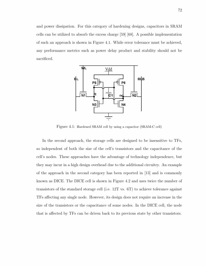
72
and power dissipation. For this category of hardening designs, capacitors in SRAM
cells can be utilized to absorb the excess charge [59] [68]. A possible implementation
of such an approach is shown in Figure 4.1. While error tolerance must be achieved,
any performance metrics such as power delay product and stability should not be
sacrificed.
Figure 4.1: Hardened SRAM cell by using a capacitor (SRAM-C cell)
In the second approach, the storage cells are designed to be insensitive to TFs,
so independent of both the size of the cell’s transistors and the capacitance of the
cell’s nodes. These approaches have the advantage of technology independence, but
they may incur in a high design overhead due to the additional circuitry. An example
of the approach in the second category has been reported in [13] and is commonly
known as DICE. The DICE cell is shown in Figure 4.2 and uses twice the number of
transistors of the standard storage cell (i.e. 12T vs. 6T) to achieve tolerance against
TFs affecting any single node. However, its design does not require an increase in the
size of the transistors or the capacitance of some nodes. In the DICE cell, the node
that is affected by TFs can be driven back to its previous state by other transistors.
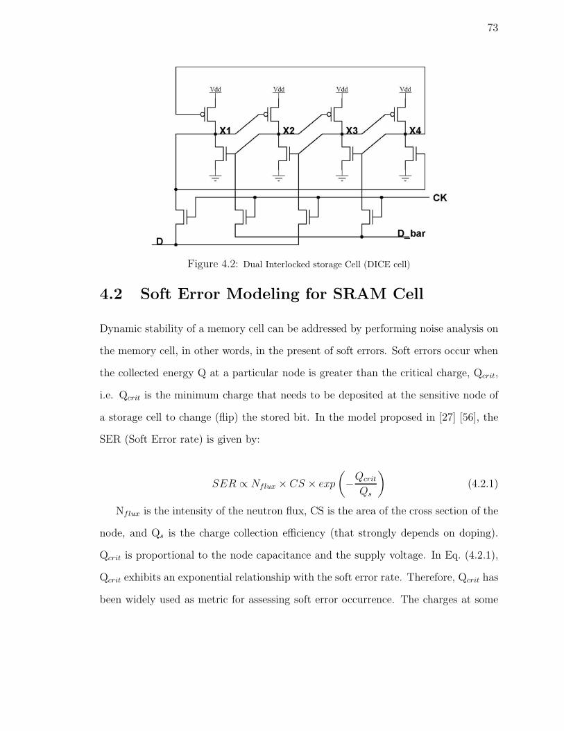
73
Figure 4.2: Dual Interlocked storage Cell (DICE cell)
4.2 Soft Error Modeling for SRAM Cell
Dynamic stability of a memory cell can be addressed by performing noise analysis on
the memory cell, in other words, in the present of soft errors. Soft errors occur when
the collected energy Q at a particular node is greater than the critical charge, Qcrit,
i.e. Qcrit is the minimum charge that needs to be deposited at the sensitive node of
a storage cell to change (flip) the stored bit. In the model proposed in [27] [56], the
SER (Soft Error rate) is given by:
SER ∝ Nflux × CS × exp
(−Qcrit
Qs
)(4.2.1)
Nflux is the intensity of the neutron flux, CS is the area of the cross section of the
node, and Qs is the charge collection efficiency (that strongly depends on doping).
Qcrit is proportional to the node capacitance and the supply voltage. In Eq. (4.2.1),
Qcrit exhibits an exponential relationship with the soft error rate. Therefore, Qcrit has
been widely used as metric for assessing soft error occurrence. The charges at some
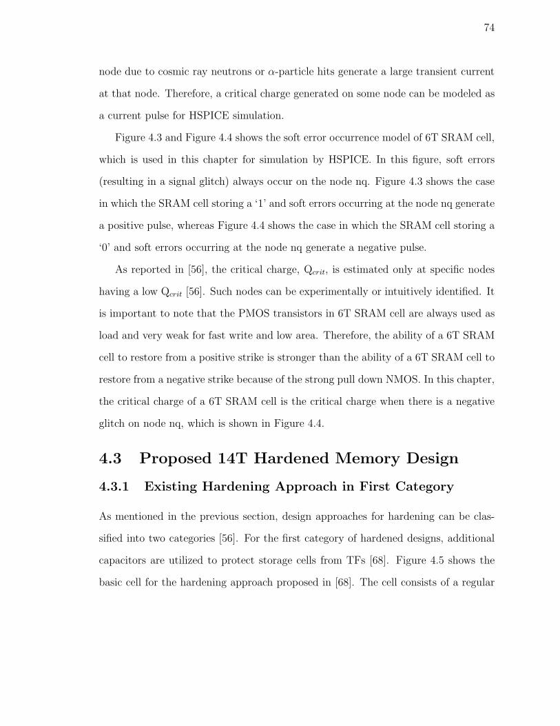
74
node due to cosmic ray neutrons or α-particle hits generate a large transient current
at that node. Therefore, a critical charge generated on some node can be modeled as
a current pulse for HSPICE simulation.
Figure 4.3 and Figure 4.4 shows the soft error occurrence model of 6T SRAM cell,
which is used in this chapter for simulation by HSPICE. In this figure, soft errors
(resulting in a signal glitch) always occur on the node nq. Figure 4.3 shows the case
in which the SRAM cell storing a ‘1’ and soft errors occurring at the node nq generate
a positive pulse, whereas Figure 4.4 shows the case in which the SRAM cell storing a
‘0’ and soft errors occurring at the node nq generate a negative pulse.
As reported in [56], the critical charge, Qcrit, is estimated only at specific nodes
having a low Qcrit [56]. Such nodes can be experimentally or intuitively identified. It
is important to note that the PMOS transistors in 6T SRAM cell are always used as
load and very weak for fast write and low area. Therefore, the ability of a 6T SRAM
cell to restore from a positive strike is stronger than the ability of a 6T SRAM cell to
restore from a negative strike because of the strong pull down NMOS. In this chapter,
the critical charge of a 6T SRAM cell is the critical charge when there is a negative
glitch on node nq, which is shown in Figure 4.4.
4.3 Proposed 14T Hardened Memory Design
4.3.1 Existing Hardening Approach in First Category
As mentioned in the previous section, design approaches for hardening can be clas-
sified into two categories [56]. For the first category of hardened designs, additional
capacitors are utilized to protect storage cells from TFs [68]. Figure 4.5 shows the
basic cell for the hardening approach proposed in [68]. The cell consists of a regular
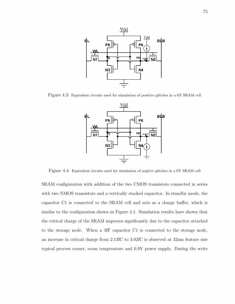
75
Figure 4.3: Equivalent circuits used for simulation of positive glitches in a 6T SRAM cell
Figure 4.4: Equivalent circuits used for simulation of negtive glitches in a 6T SRAM cell
SRAM configuration with addition of the two CMOS transistors connected in series
with two NMOS transistors and a vertically stacked capacitor. In standby mode, the
capacitor C1 is connected to the SRAM cell and acts as a charge buffer, which is
similar to the configuration shown in Figure 4.1. Simulation results have shown that
the critical charge of the SRAM improves significantly due to the capacitor attached
to the storage node. When a 3fF capacitor C1 is connected to the storage node,
an increase in critical charge from 2.13fC to 3.02fC is observed at 32nm feature size
typical process corner, room temperature and 0.9V power supply. During the write
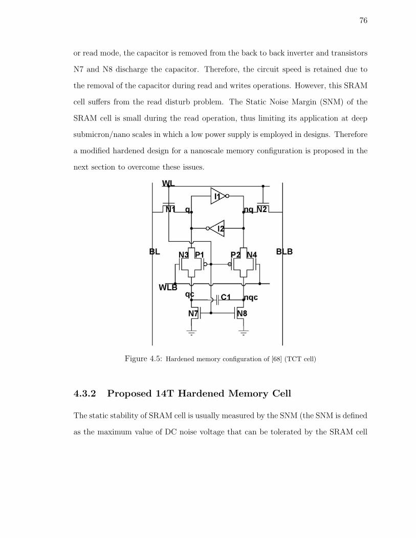
76
or read mode, the capacitor is removed from the back to back inverter and transistors
N7 and N8 discharge the capacitor. Therefore, the circuit speed is retained due to
the removal of the capacitor during read and writes operations. However, this SRAM
cell suffers from the read disturb problem. The Static Noise Margin (SNM) of the
SRAM cell is small during the read operation, thus limiting its application at deep
submicron/nano scales in which a low power supply is employed in designs. Therefore
a modified hardened design for a nanoscale memory configuration is proposed in the
next section to overcome these issues.
Figure 4.5: Hardened memory configuration of [68] (TCT cell)
4.3.2 Proposed 14T Hardened Memory Cell
The static stability of SRAM cell is usually measured by the SNM (the SNM is defined
as the maximum value of DC noise voltage that can be tolerated by the SRAM cell

77
without changing the stored bit [64]). The conventional 6T SRAM cell fails to meet
the operational requirements due to low read SNM in deep submicron/nano scale
technology. When the conventional SRAM cell is in the read operation, the pass
gate is turned on and pulls the node that stores the logic ‘0’ (for example, the node
identified by nq in Figure 4.3) to a non-zero value. This decreases the read SNM,
especially when a low power supply voltage is utilized. The hardened memory cell
shown in Figure 4.5 suffers from the so-called read-disturb problem and is rather
unstable during read operation. This memory cell achieves high performance and
dynamic stability by connecting the capacitor C1 to the storage node during the
standby mode and disconnecting the capacitor from the circuit during the operational
mode. However, it shows a very low SNM during read operation like the conventional
6T SRAM cell. Therefore, the data stored in the memory cell is very vulnerable to
external noise during the read operation.
The proposed hardened memory cell (14T) is shown in Figure 4.6. In this config-
uration, transistors N9 and N10 are added to the memory cell as access transistors
to separate the read and write operations. During read operation, RWL is high, the
data stored on nodes qc and nqc (the data on node qc and nqc are the same as the
data stored on node q and nq) are read to the bitlines such that the read operation
is fast. Meanwhile, when RWL is high and WWLB is high, the stack effect alleviates
the read disturb problem on node q or nq, thus a large read SNM is achieved in this
memory cell. The proposed hardened memory retains a high dynamic stability in
terms of critical charge (3.13fC at room temperature and 0.9V power supply), it also
achieves high static stability in terms of SNM, i.e. 250mV at room temperature and
0.9V power supply, compared to a SNM of 88.3mV for the hardened cell of Figure 4.5.
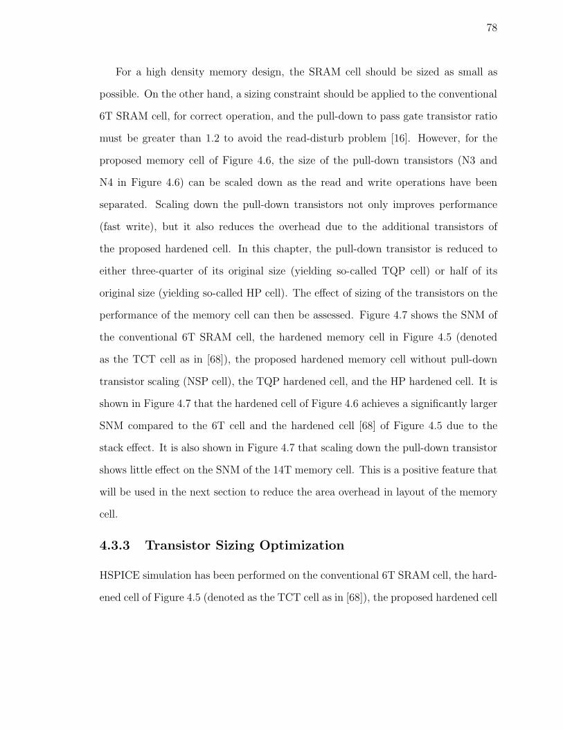
78
For a high density memory design, the SRAM cell should be sized as small as
possible. On the other hand, a sizing constraint should be applied to the conventional
6T SRAM cell, for correct operation, and the pull-down to pass gate transistor ratio
must be greater than 1.2 to avoid the read-disturb problem [16]. However, for the
proposed memory cell of Figure 4.6, the size of the pull-down transistors (N3 and
N4 in Figure 4.6) can be scaled down as the read and write operations have been
separated. Scaling down the pull-down transistors not only improves performance
(fast write), but it also reduces the overhead due to the additional transistors of
the proposed hardened cell. In this chapter, the pull-down transistor is reduced to
either three-quarter of its original size (yielding so-called TQP cell) or half of its
original size (yielding so-called HP cell). The effect of sizing of the transistors on the
performance of the memory cell can then be assessed. Figure 4.7 shows the SNM of
the conventional 6T SRAM cell, the hardened memory cell in Figure 4.5 (denoted
as the TCT cell as in [68]), the proposed hardened memory cell without pull-down
transistor scaling (NSP cell), the TQP hardened cell, and the HP hardened cell. It is
shown in Figure 4.7 that the hardened cell of Figure 4.6 achieves a significantly larger
SNM compared to the 6T cell and the hardened cell [68] of Figure 4.5 due to the
stack effect. It is also shown in Figure 4.7 that scaling down the pull-down transistor
shows little effect on the SNM of the 14T memory cell. This is a positive feature that
will be used in the next section to reduce the area overhead in layout of the memory
cell.
4.3.3 Transistor Sizing Optimization
HSPICE simulation has been performed on the conventional 6T SRAM cell, the hard-
ened cell of Figure 4.5 (denoted as the TCT cell as in [68]), the proposed hardened cell
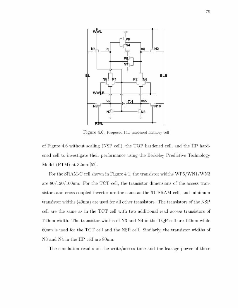
79
Figure 4.6: Proposed 14T hardened memory cell
of Figure 4.6 without scaling (NSP cell), the TQP hardened cell, and the HP hard-
ened cell to investigate their performance using the Berkeley Predictive Technology
Model (PTM) at 32nm [52].
For the SRAM-C cell shown in Figure 4.1, the transistor widths WP5/WN1/WN3
are 80/120/160nm. For the TCT cell, the transistor dimensions of the access tran-
sistors and cross-coupled inverter are the same as the 6T SRAM cell, and minimum
transistor widths (40nm) are used for all other transistors. The transistors of the NSP
cell are the same as in the TCT cell with two additional read access transistors of
120nm width. The transistor widths of N3 and N4 in the TQP cell are 120nm while
60nm is used for the TCT cell and the NSP cell. Similarly, the transistor widths of
N3 and N4 in the HP cell are 80nm.
The simulation results on the write/access time and the leakage power of these
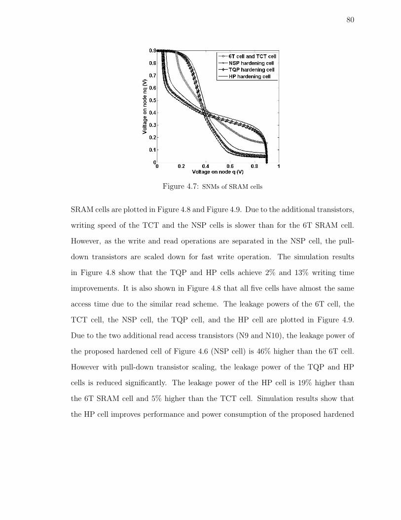
80
Figure 4.7: SNMs of SRAM cells
SRAM cells are plotted in Figure 4.8 and Figure 4.9. Due to the additional transistors,
writing speed of the TCT and the NSP cells is slower than for the 6T SRAM cell.
However, as the write and read operations are separated in the NSP cell, the pull-
down transistors are scaled down for fast write operation. The simulation results
in Figure 4.8 show that the TQP and HP cells achieve 2% and 13% writing time
improvements. It is also shown in Figure 4.8 that all five cells have almost the same
access time due to the similar read scheme. The leakage powers of the 6T cell, the
TCT cell, the NSP cell, the TQP cell, and the HP cell are plotted in Figure 4.9.
Due to the two additional read access transistors (N9 and N10), the leakage power of
the proposed hardened cell of Figure 4.6 (NSP cell) is 46% higher than the 6T cell.
However with pull-down transistor scaling, the leakage power of the TQP and HP
cells is reduced significantly. The leakage power of the HP cell is 19% higher than
the 6T SRAM cell and 5% higher than the TCT cell. Simulation results show that
the HP cell improves performance and power consumption of the proposed hardened
81
cell compared to the NSP cell. Therefore, the HP cell has the best transistor sizing
for the proposed memory cell of Figure 4.6.
Figure 4.8: Write time and access time of SRAM cells
Critical charge is often used as a metric for hardened memory designs [68]. In
the TCT cell, the NSP cell and the HP cell, the critical node (i.e. the node with the
smallest critical charge) is the same as the unhardened 6T cell, i.e. node q or nq in
Figure 4.5 and Figure 4.6. Table 4.1 summarizes the critical charge, SNM, and the
write delay of the 6T memory cell, the SRAM-C cell in Figure 4.1, the TCT cell in
Figure 4.5, the NSP cell and the HP cell in Figure 4.6. Compared to the unhardened
6T memory cell, the SRAM-C cell achieves the best critical charge, but it suffers
from a low SNM and a very slow write delay. The TCT cell achieves a high critical
charge and a fast write, but it shows a low SNM, which makes this cell very unstable
at a low power supply. The proposed NSP and the HP cells have a high critical
charge, a high SNM, and a fast write time (as shown in Table 4.1), thus making them
good candidates for high-stable and low power memory designs. In Table 4.1 shows

82
Figure 4.9: Leakage power of SRAM cells
the SNM of the HP cell is still relatively higher than the 6T and TCT cells and the
cell has a high critical charge and a faster write delay. Table 4.1 also confirms that
the transistor sizing of the HP cell is best for the proposed hardened memory cell of
Figure 4.6.
Table 4.1: Critical charge, SNM, and Performance comparison of Different Memorycells at 0.9V Power Supply and Room Temperature
Memory Cell Type Critical Charge SNM Write Delay
Unhardened 6T memory cell 2.13 fC 88.3 mV 14.66 psSRAM-C cell (C=3ff) 3.74 fC 88.3 mV 44.12 psNSP cell (C=3ff) 3.16 fC 250 mV 15.69 psHP cell (C=3ff) 3.02 fC 212.5 mV 12.81 ps
The layouts of the TCT and the HP cells (based on MOSIS deep sub-micrometer
design rules [66]) are shown in Figure 4.10 and Figure 4.11. The area of the TCT cell
is as twice as the traditional 6T SRAM cell because of the additional six transistors.
Two more transistors are added to the TCT cell [68]. The pull-down transistors’ sizes
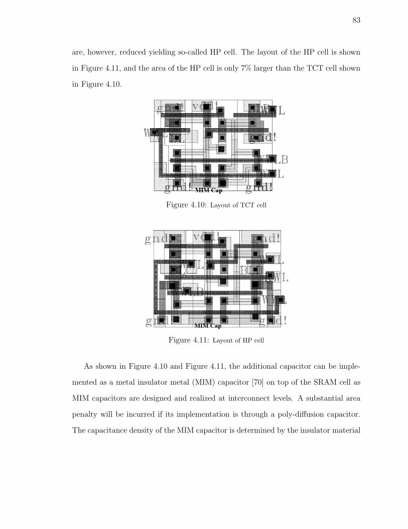
83
are, however, reduced yielding so-called HP cell. The layout of the HP cell is shown
in Figure 4.11, and the area of the HP cell is only 7% larger than the TCT cell shown
in Figure 4.10.
Figure 4.10: Layout of TCT cell
Figure 4.11: Layout of HP cell
As shown in Figure 4.10 and Figure 4.11, the additional capacitor can be imple-
mented as a metal insulator metal (MIM) capacitor [70] on top of the SRAM cell as
MIM capacitors are designed and realized at interconnect levels. A substantial area
penalty will be incurred if its implementation is through a poly-diffusion capacitor.
The capacitance density of the MIM capacitor is determined by the insulator material
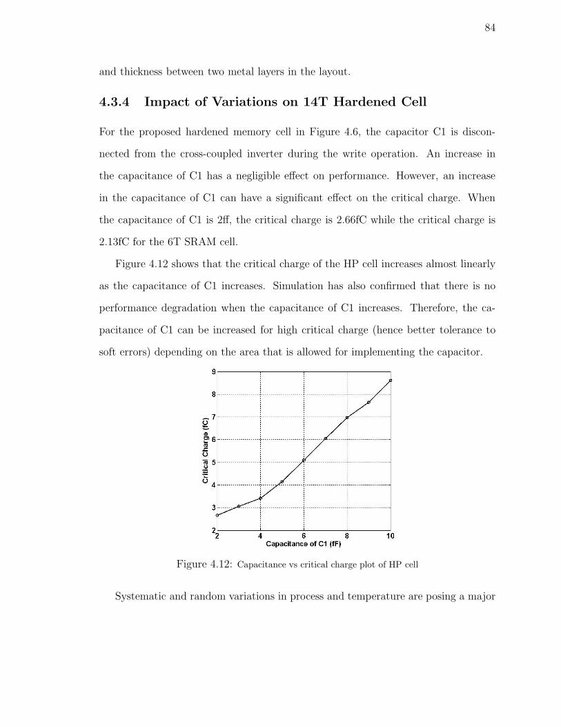
84
and thickness between two metal layers in the layout.
4.3.4 Impact of Variations on 14T Hardened Cell
For the proposed hardened memory cell in Figure 4.6, the capacitor C1 is discon-
nected from the cross-coupled inverter during the write operation. An increase in
the capacitance of C1 has a negligible effect on performance. However, an increase
in the capacitance of C1 can have a significant effect on the critical charge. When
the capacitance of C1 is 2ff, the critical charge is 2.66fC while the critical charge is
2.13fC for the 6T SRAM cell.
Figure 4.12 shows that the critical charge of the HP cell increases almost linearly
as the capacitance of C1 increases. Simulation has also confirmed that there is no
performance degradation when the capacitance of C1 increases. Therefore, the ca-
pacitance of C1 can be increased for high critical charge (hence better tolerance to
soft errors) depending on the area that is allowed for implementing the capacitor.
Figure 4.12: Capacitance vs critical charge plot of HP cell
Systematic and random variations in process and temperature are posing a major
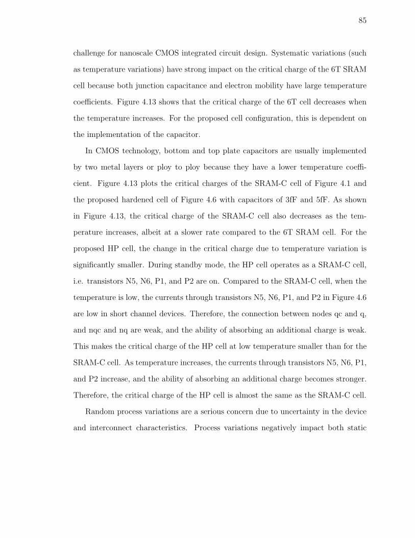
85
challenge for nanoscale CMOS integrated circuit design. Systematic variations (such
as temperature variations) have strong impact on the critical charge of the 6T SRAM
cell because both junction capacitance and electron mobility have large temperature
coefficients. Figure 4.13 shows that the critical charge of the 6T cell decreases when
the temperature increases. For the proposed cell configuration, this is dependent on
the implementation of the capacitor.
In CMOS technology, bottom and top plate capacitors are usually implemented
by two metal layers or ploy to ploy because they have a lower temperature coeffi-
cient. Figure 4.13 plots the critical charges of the SRAM-C cell of Figure 4.1 and
the proposed hardened cell of Figure 4.6 with capacitors of 3fF and 5fF. As shown
in Figure 4.13, the critical charge of the SRAM-C cell also decreases as the tem-
perature increases, albeit at a slower rate compared to the 6T SRAM cell. For the
proposed HP cell, the change in the critical charge due to temperature variation is
significantly smaller. During standby mode, the HP cell operates as a SRAM-C cell,
i.e. transistors N5, N6, P1, and P2 are on. Compared to the SRAM-C cell, when the
temperature is low, the currents through transistors N5, N6, P1, and P2 in Figure 4.6
are low in short channel devices. Therefore, the connection between nodes qc and q,
and nqc and nq are weak, and the ability of absorbing an additional charge is weak.
This makes the critical charge of the HP cell at low temperature smaller than for the
SRAM-C cell. As temperature increases, the currents through transistors N5, N6, P1,
and P2 increase, and the ability of absorbing an additional charge becomes stronger.
Therefore, the critical charge of the HP cell is almost the same as the SRAM-C cell.
Random process variations are a serious concern due to uncertainty in the device
and interconnect characteristics. Process variations negatively impact both static
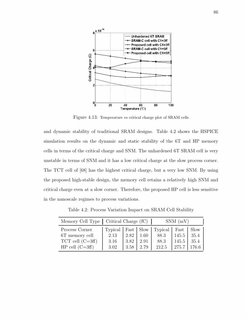
86
Figure 4.13: Temperature vs critical charge plot of SRAM cells
and dynamic stability of traditional SRAM designs. Table 4.2 shows the HSPICE
simulation results on the dynamic and static stability of the 6T and HP memory
cells in terms of the critical charge and SNM. The unhardened 6T SRAM cell is very
unstable in terms of SNM and it has a low critical charge at the slow process corner.
The TCT cell of [68] has the highest critical charge, but a very low SNM. By using
the proposed high-stable design, the memory cell retains a relatively high SNM and
critical charge even at a slow corner. Therefore, the proposed HP cell is less sensitive
in the nanoscale regimes to process variations.
Table 4.2: Process Variation Impact on SRAM Cell Stability
Memory Cell Type Critical Charge (fC) SNM (mV)
Process Corner Typical Fast Slow Typical Fast Slow6T memory cell 2.13 2.82 1.60 88.3 145.5 35.4TCT cell (C=3ff) 3.16 3.82 2.91 88.3 145.5 35.4HP cell (C=3ff) 3.02 3.58 2.79 212.5 275.7 176.6
87
4.4 Existing Hardened Memory Design in Second
Category
4.4.1 DICE Cell
As mentioned in the previous section, an example of the approach in the second
category has been reported in [13] and is commonly known as DICE. As shown in
Figure 4.2, the DICE cell uses twice the number of transistors of a standard storage
cell. The DICE cell has two states, the ‘0’ state (X1=0, X2=1, X3=0, X4=1) and the
‘1’ state (X1=1, X2=0, X3=1, X4=0). In any of these two states upon the occurrence
of a soft error (on a single node), the state of the node is always driven back to its
original value. For example, in the ‘0’ state, if the node struck by a particle is X2,
the state of X2 goes from ‘1’ to ‘0’. However, this strike will not propagate along the
feedback loop due to the interlocked configuration. Meanwhile, the state ‘0’ stored in
X1 can restore the state of X2.
4.4.2 Hardened Cell Proposed in [47]
Besides DICE cell, Figure 4.14 shows the basic cell for the hardening approach pro-
posed in [47]. This also belongs to the second category of hardened designs described
previously. Three basic principles are applicable to the design of this cell: 1) the feed-
back loop of the cell is blocked to keep the transient pulse from propagating along the
loop, 2) the gates of the NMOS and PMOS transistors of the inverters are separated
to harden those nodes left unprotected by the first principle, and 3) the regeneration
principle should be introduced to avoid the loss of stored information.
A traditional memory cell configuration uses two back to back inverters, produc-
ing a positive feedback loop to make a bistable circuit. For the radiation hardened

88
Figure 4.14: Hardening approach proposed in [47]
design in Figure 4.14, the feedback loop is blocked to prevent the transient pulse from
propagating along the loop. As shown in Figure 4.14, transistors Tpr and Tnr are used
to block the transient pulse affecting node B or node Q. Therefore, the transient pulse
cannot be propagated to nodes a1 and a2, which are the gates of transistors Tp1 and
Tn1. Furthermore, the gates of transistors Tp1 and Tn1 are separated to harden nodes
a1 and a2. As ionizing particles striking the NMOS transistor produce only negative
current pulses and ionizing particles striking a PMOS transistor produce only positive
current pulses, a particle striking node a2 can turn transistor Tn1 off, but it can never
turn it on. Similarly, a particle striking node a1 can turn transistor Tp1 off, but it can

89
never turn it on. Turning Tp1 or Tn1 off can only bring the output of the first inverter
to the high impedance state, thus leaving unaffected the previous state at node B.
Therefore, TFs on nodes a1 and a2 are also blocked. The gate control voltages Vp
and Vn are applied to the transistors Tpr and Tnr to restore the values by the leakage
current on nodes a1 and a2 as proposed in [47].
It is shown in [60] that there is an exponential relationship between the gate
voltage and the leakage current. Therefore, to increase the leakage current of Tpr
and Tnr, the voltages Vp = Vdd − d and Vn = d (where d is equal to a few tenth of
Vdd) are applied to the gates of Tpr and Tnr, respectively [47]. However, the leakage
current also decreases significantly as the drain source voltage decreases. Assume the
voltage at a1 and a2 is Vdd and a negative strike occurs on node a2. Simulation by
HSPICE shows that for 0.9V power supply the node a2 can be promptly restored
to 0.2V due to the large voltage difference between source and drain. However, the
voltage at node a2 increases slowly after the voltage reaches 0.2V due to the reduced
drain source voltage difference. Therefore, the voltage at node a2 can be only driven
to approximately 0.25V instead of 0.9V. Similarly, the voltage for ‘0’ data at node
a1 can be only driven back to approximately 0.65V (high state) if a positive strike
occurs on node a1 and (storing a logic ‘0’). Therefore, the DC voltages at Vp and Vn
are unable to restore the node voltage after the nodes are struck by a transient pulse.
To fully restore the voltages at nodes a1 and a2, the periodic signals Vp = Rn’ and
Vn = Rn have been also utilized as proposed in [47]. The periodic signal Rn is ‘0’ for
most of the time and it takes the value of ‘1’ for a short time to restore the value of
node a2. The signal Rn’ is used in a similar fashion.
As shown in Figure 4.15, a hardened memory cell has also been proposed in [47]
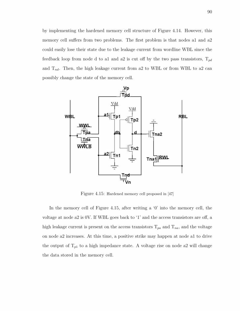
90
by implementing the hardened memory cell structure of Figure 4.14. However, this
memory cell suffers from two problems. The first problem is that nodes a1 and a2
could easily lose their state due to the leakage current from wordline WBL since the
feedback loop from node d to a1 and a2 is cut off by the two pass transistors, Tpd
and Tnd. Then, the high leakage current from a2 to WBL or from WBL to a2 can
possibly change the state of the memory cell.
Figure 4.15: Hardened memory cell proposed in [47]
In the memory cell of Figure 4.15, after writing a ‘0’ into the memory cell, the
voltage at node a2 is 0V. If WBL goes back to ‘1’ and the access transistors are off, a
high leakage current is present on the access transistors Tpa and Tna, and the voltage
on node a2 increases. At this time, a positive strike may happen at node a1 to drive
the output of Tp1 to a high impedance state. A voltage rise on node a2 will change
the data stored in the memory cell.
91
The second problem of this memory cell is the signal distribution network of Vp
and Vn since Vp = Vdd − d and Vn = d (where d can be equal to a few tenth of
Vdd) or the periodic signals Vp = Rn’ and Vn = Rn, must be applied to every single
memory cell as mentioned before. The signal generation and distribution are very
costly, and they result in an additional load to the overall memory, thus degrading
its performance.
For hardening design, the scheme shown in Figure 4.14 can be still utilized even for
a different memory cell configuration to overcome the problems described previously.
This is described in more detail in the next section.
4.5 Proposed 11T Hardened Memory Design
A new hardened memory cell is proposed in this chapter to overcome the problems
described previously. Its design is shown in Figure 4.16 and solves the problems
described in the previous section for the design of [47].
The proposed hardened cell is derived and improved from the fast hardened latch
in [47] by removing the switches in the feedback loop. As mentioned in the previous
section, the hardened memory proposed in [47] has two problems which affect the
correct operation of the cell. The feedback configuration in the fast hardened latch in
[47] is found to be better suitable for hardened memory cell than the feedback in the
hardened memory in [47]. The basic storage element used in the proposed hardened
memory cell relies on the hardening scheme [47] of Figure 4.14. In the hardened
memory cell of Figure 4.16, the feedback loop in the memory cell is cut off by the
transistors M5, M6, M7, and M8, i.e. a transient pulse cannot be propagated along
this loop back to its starting point. At the unprotected nodes a1 and a2, the gates
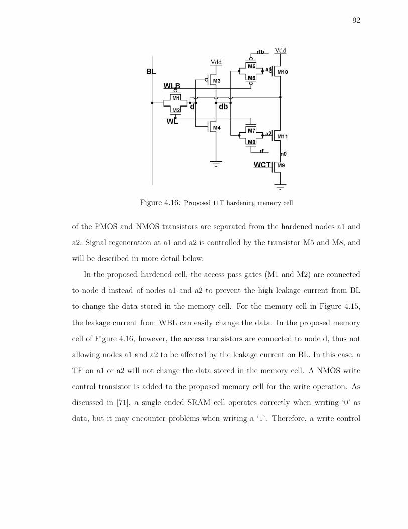
92
Figure 4.16: Proposed 11T hardening memory cell
of the PMOS and NMOS transistors are separated from the hardened nodes a1 and
a2. Signal regeneration at a1 and a2 is controlled by the transistor M5 and M8, and
will be described in more detail below.
In the proposed hardened cell, the access pass gates (M1 and M2) are connected
to node d instead of nodes a1 and a2 to prevent the high leakage current from BL
to change the data stored in the memory cell. For the memory cell in Figure 4.15,
the leakage current from WBL can easily change the data. In the proposed memory
cell of Figure 4.16, however, the access transistors are connected to node d, thus not
allowing nodes a1 and a2 to be affected by the leakage current on BL. In this case, a
TF on a1 or a2 will not change the data stored in the memory cell. A NMOS write
control transistor is added to the proposed memory cell for the write operation. As
discussed in [71], a single ended SRAM cell operates correctly when writing ‘0’ as
data, but it may encounter problems when writing a ‘1’. Therefore, a write control

93
transistor is added between M11 and ground and the WCT signal is generated by
the write select signal [71]. When the column is selected, the WCT signal is low and
the pull down transistor does not affect the write operation. As for the unselected
columns, the WCT signal is high to maintain the latch function. With the new write
control transistor, the proposed hardened memory cell consists of eleven transistors,
which is one transistor less than the DICE configuration.
The refresh signals rf and rfb are connected to the gates of M8 and M5 to regen-
erate the states at nodes a1 and a2. As described in Section 4.4.2, the voltages Vp =
Vdd - d and Vn = d on transistors Tpd and Tnd of Figure 4.15 are unable to restore the
voltages at nodes a1 and a2, and this also causes a high standby power consumption
for the memory cell. Therefore, the periodic refresh signals Vp = Rn’ and Vn = Rn
must be used to regenerate the states on nodes a1 and a2. As the read wordline is
always connected to the memory cell, then these two signals can be used to control
the pass gate transistors to block the feedback loop. As shown in Figure 4.17, when
WL is high and WLB is low, the transistors M7 and M6 are on, and the cell acts
as a normal memory element. When WL is low and WLB is high, the transistors
M7 and M6 are off, and the feedback loop is cut off. The refresh signals, rf and rfb,
are generated by the read select signal. When a column is selected for read, the rf
and rfb signals are generated at each column by a complementary pulse generator to
refresh the data at the nodes a1 and a2 and ensure that the correct signal is read by
the bitline. The memory design proposed in this chapter successfully addresses both
problems described previously for the cell of [47].
As the access transistors M1 and M2 are used for both (read and write) operations,
the refresh transistors M5 and M8 and the refresh signals rf and rfb ensure a correct

94
read operation. As shown in Figure 4.17, when the memory stores ‘0’ as data, a2 is
‘1’. Consider the scenario in which a TF occurs on node a2 prior to the read operation
thus driving node a2 to a ‘0’ state. As discussed in Section 4.4.2, the state of node
a2 needs to be restored. Otherwise during the read operation, M6 and M7 are on.
The ‘0’ state on node a2 will change the data on nodes db and a1 to the ‘0’ state,
resulting in data change on node d to a ‘1’ (its correct value is ‘0’). If there is no
refresh prior to the read operation, an error occurs during the read operation if a TF
strikes on node a2. Therefore, the refresh signals rf and rfb generated by the read
select signal are connected to M8 and M5 to refresh the memory cell before the read
operation. The refresh operation is performed by a pulse generator circuit locally
sited at every column to provide the refresh signal; once the column is accessed for a
read operation, the refresh signal is generated to refresh the memory cells. Simulation
results using HSPICE show that adding the refresh transistors and the refresh circuit
to the proposed hardened cell will only increase the average power consumption by
0.8% per single cell during the read access operation. The power dissipation of this
pulse generator circuit (consisting of a dozen transistors) is very small and therefore
negligible compared to the entire memory array. It is important to note that the
read column select signal for generating rf and rfb must arrive earlier than the read
wordline. This condition is always valid in the proposed design.
4.6 Evaluation of the Proposed 11T Hardened Cell
In this section, different figures of merit as related to critical charge, power dissipation
and delay are assessed to compare the proposed memory cell with other schemes found
in the technical literature.
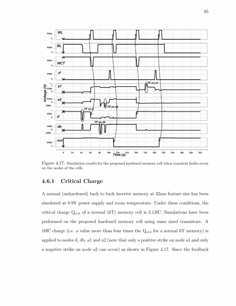
95
Figure 4.17: Simulation results for the proposed hardened memory cell when transient faults occuron the nodes of the cells
4.6.1 Critical Charge
A normal (unhardened) back to back inverter memory at 32nm feature size has been
simulated at 0.9V power supply and room temperature. Under these conditions, the
critical charge Qcrit of a normal (6T) memory cell is 2.13fC. Simulations have been
performed on the proposed hardened memory cell using same sized transistors. A
10fC charge (i.e. a value more than four times the Qcrit for a normal 6T memory) is
applied to nodes d, db, a1 and a2 (note that only a positive strike on node a1 and only
a negative strike on node a2 can occur) as shown in Figure 4.17. Since the feedback
96
loop is blocked, a TF on node d or db will not propagate to its starting point, so the
stored data will be unaffected. If there is a strike on node a1 or a2, the output of
the first inverter will be at the high impedance state and the data on nodes d and db
will not be changed. When the periodic refresh signal arrives, the voltage on node
a1 or a2 is then restored to its previous state. Simulation results show that the data
stored in the proposed hardened memory cell does not change even when a transient
pulse with a charge higher than 10fC is applied to the nodes. Same as the DICE cell,
the proposed design presents complete immunity for any transient on a single node
regardless of the strength of the transient fault. Therefore, this design is hardened
and excellent tolerance to soft errors is accomplished.
4.6.2 Area, Power and Delay
The proposed hardened memory has eleven transistors compared to a conventional
memory that has only six transistors (6T). The additional transistors consume more
power depending on the choice of technology. In the proposed hardened memory
cell, the write operation can be slowed down due the transistors for blocking the
feedback loop. In the proposed memory cell design of Figure 4.16, the size of the
access transistors is therefore increased to improve performance. Figure 4.18 shows
the write delay of the proposed 11-transistor hardened memory cell, the DICE cell
(12T), and the 6T conventional memory cell. The width of the access transistors M1
and M2 in Figure 4.16 is twice the width of the access transistors of the DICE cell and
a 6T conventional memory cell. As shown in Figure 4.18, both the write ‘0’ and the
write ‘1’ delays of the proposed 11T hardened memory cell are the fastest. However,
this results in an increase of power consumption. Therefore, the power-delay product
of the hardened memory cells (as an important metric for digital CMOS circuits)
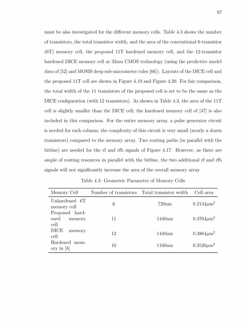
97
must be also investigated for the different memory cells. Table 4.3 shows the number
of transistors, the total transistor width, and the area of the conventional 6-transistor
(6T) memory cell, the proposed 11T hardened memory cell, and the 12-transistor
hardened DICE memory cell at 32nm CMOS technology (using the predictive model
data of [52] and MOSIS deep sub-micrometer rules [66]). Layouts of the DICE cell and
the proposed 11T cell are shown in Figure 4.19 and Figure 4.20. For fair comparison,
the total width of the 11 transistors of the proposed cell is set to be the same as the
DICE configuration (with 12 transistors). As shown in Table 4.3, the area of the 11T
cell is slightly smaller than the DICE cell; the hardened memory cell of [47] is also
included in this comparison. For the entire memory array, a pulse generator circuit
is needed for each column; the complexity of this circuit is very small (nearly a dozen
transistors) compared to the memory array. Two routing paths (in parallel with the
bitline) are needed for the rf and rfb signals of Figure 4.17. However, as there are
ample of routing resources in parallel with the bitline, the two additional rf and rfb
signals will not significantly increase the area of the overall memory array.
Table 4.3: Geometric Parameter of Memory Cells
Memory Cell Number of transistors Total transistor width Cell area
Unhardened 6Tmemory cell
6 720nm 0.2134μm2
Proposed hard-ened memorycell
11 1440nm 0.3764μm2
DICE memorycell
12 1440nm 0.3864μm2
Hardened mem-ory in [8]
10 1160nm 0.3520μm2

98
Figure 4.18: Write delay of memory cells at different temperatures
HSPICE simulation has been performed at a 0.9V power supply and room tem-
perature using the Berkeley Predictive Technology Model at 32nm [52]. Figure 4.21
shows the simulation results for the standby power and the write delay product of
the two hardened memory cells and the conventional 6T memory cell at different
process corners. For the proposed 11-transistor hardened memory cell, the worst case
standby power is measured, i.e. when BL is high and the memory cell stores a ‘0’.
For the write delay, the average delay of the write ‘1’ and ‘0’ operations is used for the
power delay product (PDP). The power delay product of the proposed 11-transistor
hardened memory cell is 38% higher than the power delay product of the 6T (un-
hardened) memory cell due to the additional transistors. The DICE cell has 218%
increases in the power delay product with respect to the 6T memory cell due to the
large leakage current from the four access transistors. Therefore, by combining the
delay improvement and power overhead, the proposed 11-transistor hardened memory
cell has a 55% reduction in power delay product compared with the DICE cell. The

99
Figure 4.19: Layout of DICE cell
Figure 4.20: Layout of Proposed 11T cell
HSPICE simulation results (plotted in Figure 4.21) confirm the reduction in power
delay product at different process corners.
4.6.3 Impact of Process Variation
Using Monte Carlo and HSPICE, the soft-error tolerance of the proposed hardened
memory cell is evaluated in the presence of process variations in the channel length
and the threshold voltage of the transistors.
In the Monte Carlo simulation, transient faults on internal nodes of the memory
cell follow a uniform distribution in the Monte Carlo simulation. In the presence
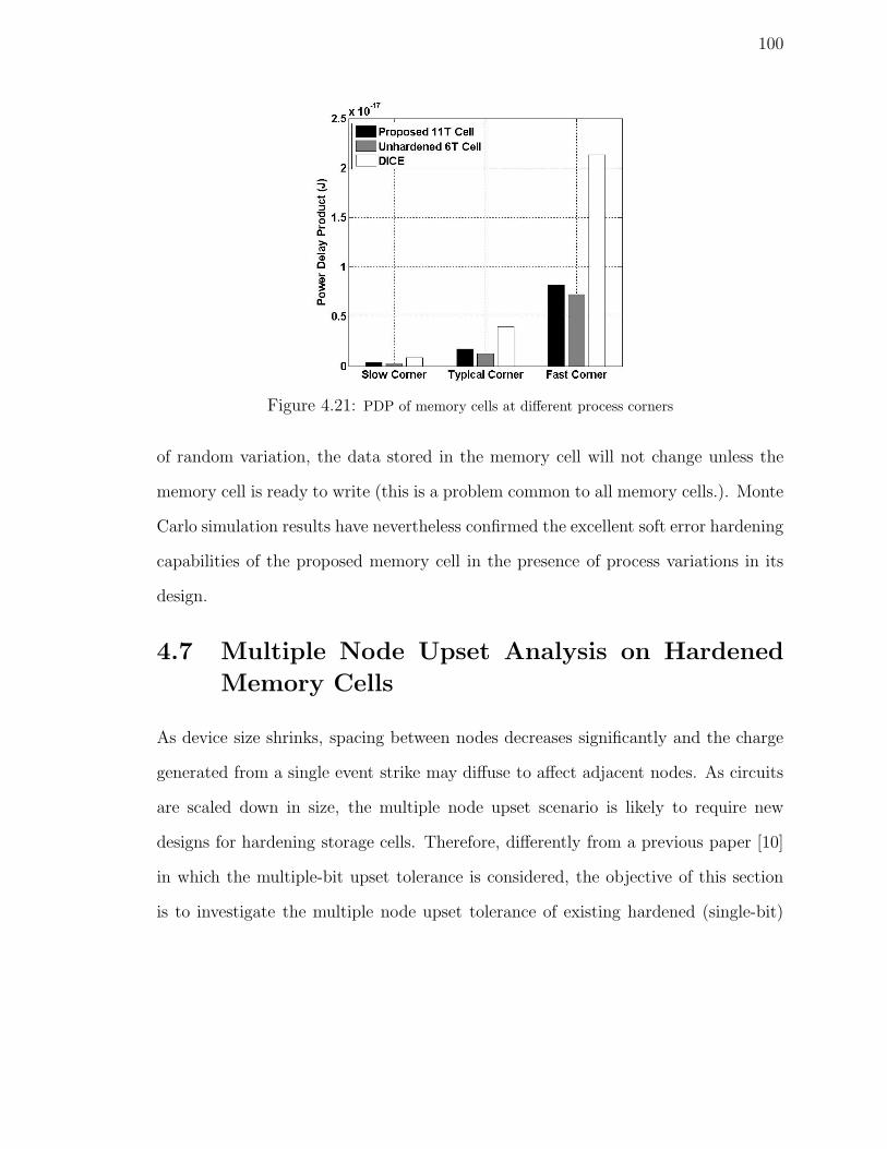
100
Figure 4.21: PDP of memory cells at different process corners
of random variation, the data stored in the memory cell will not change unless the
memory cell is ready to write (this is a problem common to all memory cells.). Monte
Carlo simulation results have nevertheless confirmed the excellent soft error hardening
capabilities of the proposed memory cell in the presence of process variations in its
design.
4.7 Multiple Node Upset Analysis on Hardened
Memory Cells
As device size shrinks, spacing between nodes decreases significantly and the charge
generated from a single event strike may diffuse to affect adjacent nodes. As circuits
are scaled down in size, the multiple node upset scenario is likely to require new
designs for hardening storage cells. Therefore, differently from a previous paper [10]
in which the multiple-bit upset tolerance is considered, the objective of this section
is to investigate the multiple node upset tolerance of existing hardened (single-bit)
101
memories and propose new hardened design with better multiple node upset tolerance.
4.7.1 Multiple Node Upset Modeling
As described in Section 4.2, the soft error on the critical node is modeled as a current
source injected to that node. For multiple node injection, multiple current sources
are applied to the circuit nodes. A multiple node upset occurs when more than one
node are affected in the storage element and additional charge is collected by those
nodes. It is also important to note that only the two-node upset scenario is modeled
in this section. A multiple upset scenario with more than two nodes is unlikely to
cause a significant state change due to the extensive charge diffusion occurring in
the storage element and wider spread of the incident strike [10]. Therefore, the node
that collects the primary portion of the charge is referred to as the primary node,
while the node that collects the remaining portion of the charge is referred to as the
secondary node. To simulate the charge collection on two adjacent nodes, the charge
is deposited simultaneously on node pairs using multiple current sources [67]; this
simulation-based approach has been verified to yield the same correct results as a 3D
device modeling approach [67].
Therefore, to investigate the tolerance to the multiple node upset scenario outlined
previously, two independent current sources are applied to the cell nodes to find the
worst case combination for a memory cell. In this section, this is referred to as the
critical pair; the critical pair defines two types of information: (a) the nodes that
are affected by the soft error and its transient fault; (b) the original and final states
of the nodes. In theory for a memory cell with N nodes, there are at most 2N(N-1)
combinations; in practice the number of combinations is much less as dependent on
the cell functionality and circuit structure. For example, a conventional 6T cell has
102
two internal nodes that may be affected by a particle strike, hence there are four
combinations. For the DICE cell, there are 24 combinations, but only transient faults
on adjacent nodes will cause a multiple node upset (due to its feedback feature). So,
the number of combinations for the DICE cell is reduced to 16. For the 11T memory
cell of in Figure 4.16, particles striking the NMOS transistor produce only negative
current pulses and particles striking a PMOS transistor produce only positive current
pulses. So, a particle striking node a2 can turn transistor M11 off, but it can never
turn it on, i.e. node a2 can only go from state 1 to 0, but never from 0 to 1. Similarly,
a particle striking node a1 can turn transistor M10 off, but it can never turn it on.
Therefore, the number of combinations of the 11T cell is 12.
The process for finding the critical pair of a hardened storage element can start
from the critical node (as the node with the lowest critical charge). This node is
therefore identified as the primary node. All combinations related to the primary
node are then simulated and the critical pair is found. However, for the 11T and
the DICE memory cells, they are fully immune to a single node upset. In this case,
simulation of all possible combinations must be performed to find the critical pair.
The exhaustive pair-wise node simulation of these memory cells has been performed
and the results show that the critical pair for the DICE cell is “X1 1->0 (i.e. the
state of node X1 changes from ‘1’ to ‘0’), X4 0->1”, and the primary node for this
pair is node X1. Similarly, the critical pair for the 11T memory cell is “a2 1->0, d
0->1”. Simulation results show that the 11T memory is more vulnerable to multiple
node upsets compared with DICE. To improve its tolerance to multiple node upsets,
two transistors are added to the 11T memory cell, yielding a 13T memory design,
which will be described in more detail in the next section.
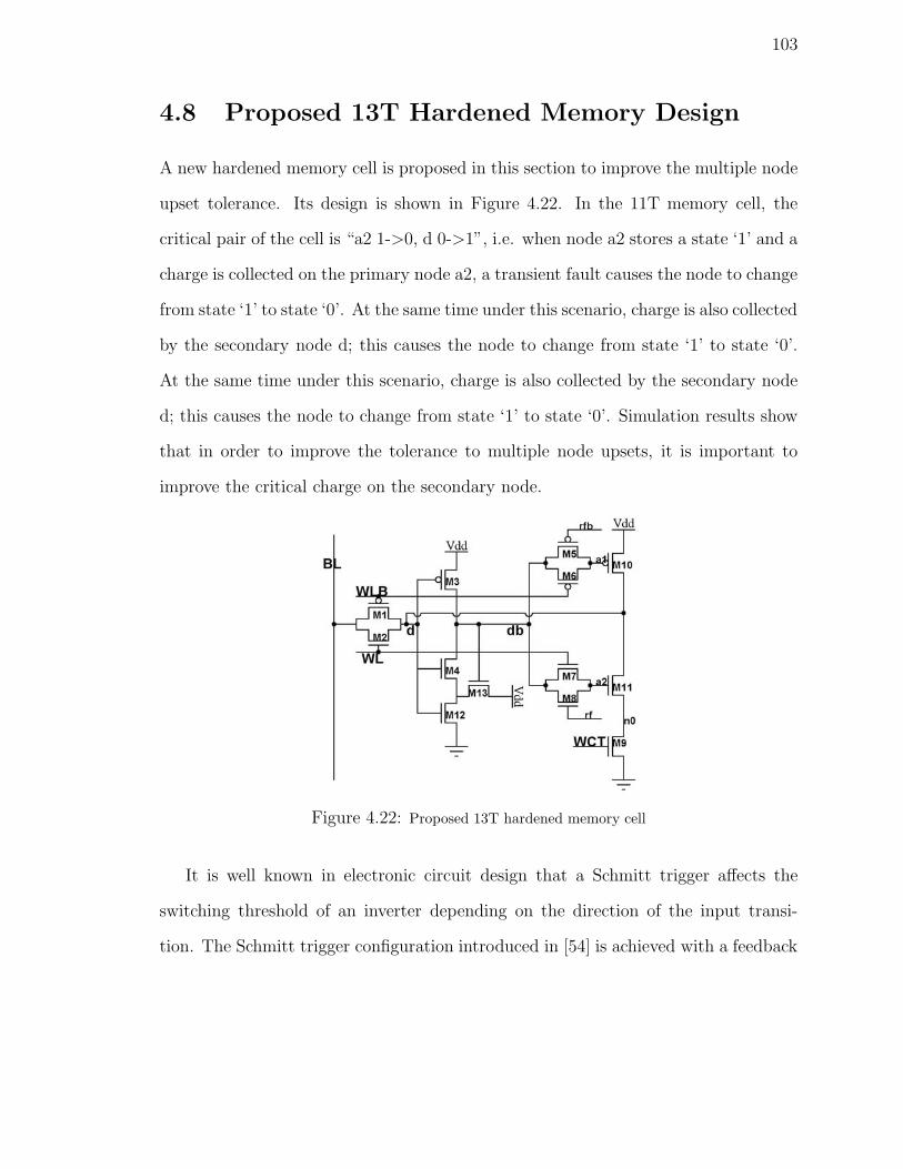
103
4.8 Proposed 13T Hardened Memory Design
A new hardened memory cell is proposed in this section to improve the multiple node
upset tolerance. Its design is shown in Figure 4.22. In the 11T memory cell, the
critical pair of the cell is “a2 1->0, d 0->1”, i.e. when node a2 stores a state ‘1’ and a
charge is collected on the primary node a2, a transient fault causes the node to change
from state ‘1’ to state ‘0’. At the same time under this scenario, charge is also collected
by the secondary node d; this causes the node to change from state ‘1’ to state ‘0’.
At the same time under this scenario, charge is also collected by the secondary node
d; this causes the node to change from state ‘1’ to state ‘0’. Simulation results show
that in order to improve the tolerance to multiple node upsets, it is important to
improve the critical charge on the secondary node.
Figure 4.22: Proposed 13T hardened memory cell
It is well known in electronic circuit design that a Schmitt trigger affects the
switching threshold of an inverter depending on the direction of the input transi-
tion. The Schmitt trigger configuration introduced in [54] is achieved with a feedback

104
mechanism to increase the switching threshold of the input inverter [54]. Since the
transition on node d is from ‘1’ to ‘0’, in the proposed design the feedback mechanism
is used only in the pull-down path to improve the critical charge on the secondary
node, i.e. node d.
As shown in Figure 4.22, two additional transistors are added to the 11T memory
cell, yielding a 13T design. The operation of the 13T memory cell is similar to the
11T memory cell. The refresh signals rf and rfb are connected to the gates of M8 and
M5 to regenerate the states at nodes a1 and a2. The periodic refresh signals Vp =
Rn’ and Vn = Rn are used to regenerate the states on nodes a1 and a2. As the read
wordline is always connected to the memory cell, then these two signals can be used
to control the pass gate transistors to block the feedback loop.
Figure 4.23 shows the timing diagram of the proposed 13T memory cell. The
read and write mechanism of the 13T memory cell is similar to the 11T memory
cell. When WL is high, the transistors M7 and M6 are on, and the cell acts as a
normal memory element. When WL is low, the transistors M7 and M6 are off, and
the feedback loop is cut off. The refresh signals, rf and rfb, are generated by the read
select signal. When a column is selected for read, the rf and rfb signals are generated
by a complementary pulse generator to refresh the data at the nodes a1 and a2 and
ensure that the correct signal is read by the bitline BL.
4.9 Evaluation of the 13T Memory Cell
In this section, different figures of merit as related to critical charge, power dissipation
and delay are assessed to compare the proposed memory cell with other schemes found
in the technical literature.
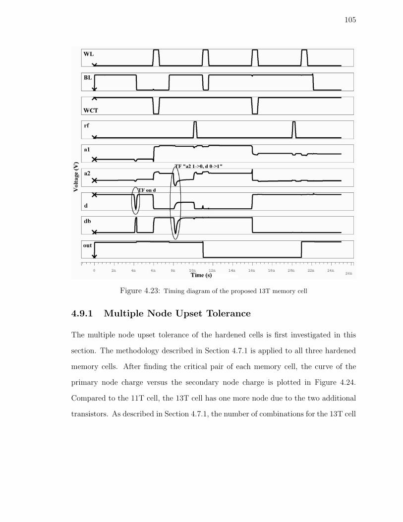
105
Figure 4.23: Timing diagram of the proposed 13T memory cell
4.9.1 Multiple Node Upset Tolerance
The multiple node upset tolerance of the hardened cells is first investigated in this
section. The methodology described in Section 4.7.1 is applied to all three hardened
memory cells. After finding the critical pair of each memory cell, the curve of the
primary node charge versus the secondary node charge is plotted in Figure 4.24.
Compared to the 11T cell, the 13T cell has one more node due to the two additional
transistors. As described in Section 4.7.1, the number of combinations for the 13T cell
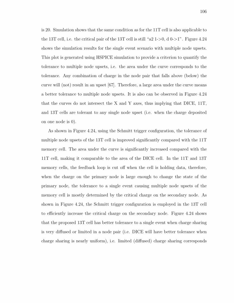
106
is 20. Simulation shows that the same condition as for the 11T cell is also applicable to
the 13T cell, i.e. the critical pair of the 13T cell is still “a2 1->0, d 0->1”. Figure 4.24
shows the simulation results for the single event scenario with multiple node upsets.
This plot is generated using HSPICE simulation to provide a criterion to quantify the
tolerance to multiple node upsets, i.e. the area under the curve corresponds to the
tolerance. Any combination of charge in the node pair that falls above (below) the
curve will (not) result in an upset [67]. Therefore, a large area under the curve means
a better tolerance to multiple node upsets. It is also can be observed in Figure 4.24
that the curves do not intersect the X and Y axes, thus implying that DICE, 11T,
and 13T cells are tolerant to any single node upset (i.e. when the charge deposited
on one node is 0).
As shown in Figure 4.24, using the Schmitt trigger configuration, the tolerance of
multiple node upsets of the 13T cell is improved significantly compared with the 11T
memory cell. The area under the curve is significantly increased compared with the
11T cell, making it comparable to the area of the DICE cell. In the 11T and 13T
memory cells, the feedback loop is cut off when the cell is holding data, therefore,
when the charge on the primary node is large enough to change the state of the
primary node, the tolerance to a single event causing multiple node upsets of the
memory cell is mostly determined by the critical charge on the secondary node. As
shown in Figure 4.24, the Schmitt trigger configuration is employed in the 13T cell
to efficiently increase the critical charge on the secondary node. Figure 4.24 shows
that the proposed 13T cell has better tolerance to a single event when charge sharing
is very diffused or limited in a node pair (i.e. DICE will have better tolerance when
charge sharing is nearly uniform), i.e. limited (diffused) charge sharing corresponds
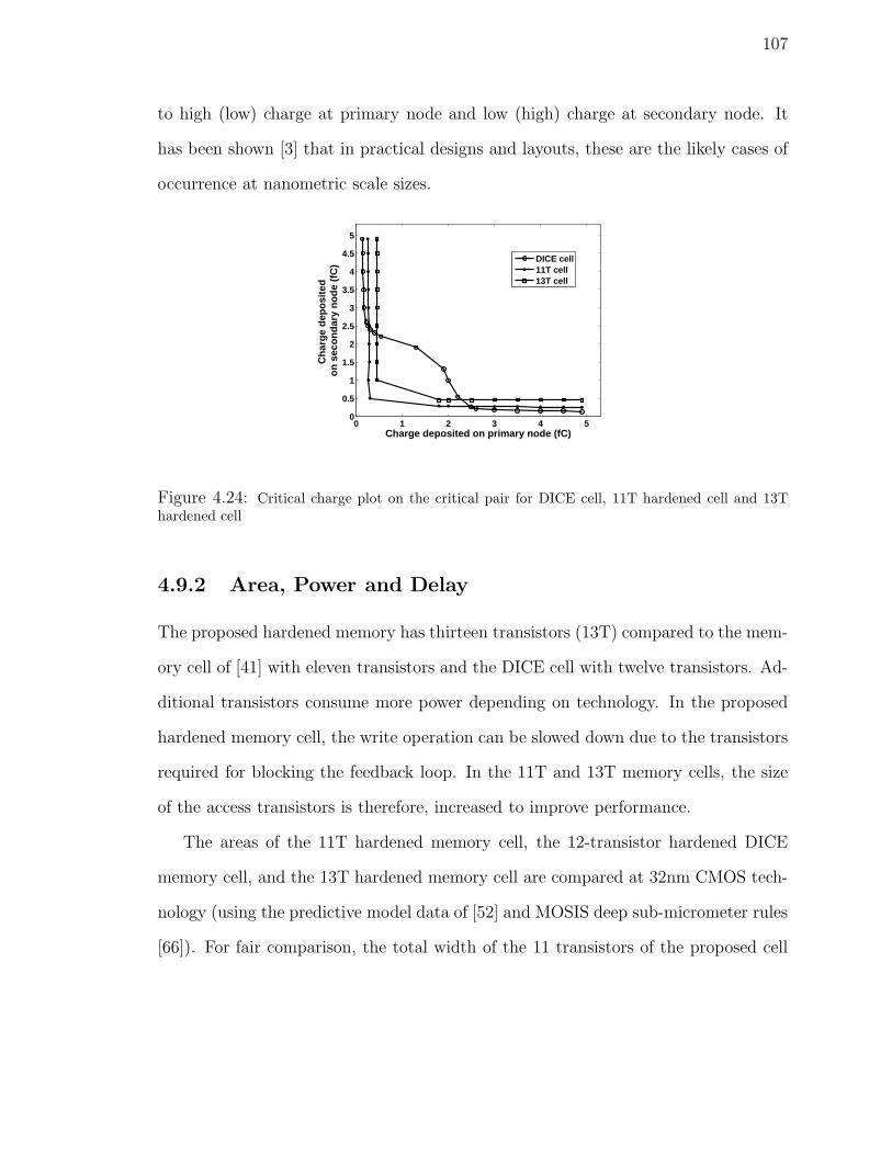
107
to high (low) charge at primary node and low (high) charge at secondary node. It
has been shown [3] that in practical designs and layouts, these are the likely cases of
occurrence at nanometric scale sizes.
0 1 2 3 4 50
0.5
1
1.5
2
2.5
3
3.5
4
4.5
5
Charge deposited on primary node (fC)
Ch
arg
e d
epo
site
d
on
sec
on
dar
y n
od
e (f
C)
DICE cell11T cell13T cell
Figure 4.24: Critical charge plot on the critical pair for DICE cell, 11T hardened cell and 13Thardened cell
4.9.2 Area, Power and Delay
The proposed hardened memory has thirteen transistors (13T) compared to the mem-
ory cell of [41] with eleven transistors and the DICE cell with twelve transistors. Ad-
ditional transistors consume more power depending on technology. In the proposed
hardened memory cell, the write operation can be slowed down due to the transistors
required for blocking the feedback loop. In the 11T and 13T memory cells, the size
of the access transistors is therefore, increased to improve performance.
The areas of the 11T hardened memory cell, the 12-transistor hardened DICE
memory cell, and the 13T hardened memory cell are compared at 32nm CMOS tech-
nology (using the predictive model data of [52] and MOSIS deep sub-micrometer rules
[66]). For fair comparison, the total width of the 11 transistors of the proposed cell
108
is the same as the DICE configuration (with 12 transistors). So, the width of the
access transistors M1 and M2 in Figure 4.22 is twice the width of the access transis-
tors of the DICE cell. Figure 4.25 shows the write delay, the access delay, the power
consumption, and the area of the 11T memory cell, the DICE cell (12T), and the
proposed 13T memory cell. The write delay shown in Figure 4.25 is the average of
the write ‘0’ delay and the write ‘1’ delay. The access delay shown in Figure 4.25 is
the average of the read ‘0’ delay and the read ‘1’ delay. All four figures of merit have
been normalized to the ones for the conventional (unhardened) 6T memory cell. Due
to the large access transistors, the delay performance of the 11T and 13T memory
cell is improved, at a higher power consumption, and larger area. In Figure 4.25, the
proposed 13T cell is 33% faster than the DICE cell, with only a 3% higher area and
a 5% power penalty.
Figure 4.25: Performance, power, and area comparison of the DICE, 11T and 13T cells
For advanced technologies, the shorter distance between node diffusions results
in diffusion of charges to adjacent nodes other than the hit node. The greater the
distance is, the lower the possibility of multiple node upsets. Therefore, multiple

109
node charge collection is a strong function of the cell layout. Layout of DICE cell is
shown in Figure 4.19 and proposed 13T cell is shown in Figure 4.26. The minimum
distance of critical pair of the DICE cell (x1 to x4) and 13T cell (d to a2) is also
shown in Figure 4.19 and Figure 4.26. The area of the 13T cell is 9% higher than
the area of DICE cell; however, the distance of the critical pair (d, a2) in 13T cell
is 14% longer than the distance of the critical pair (x1, x4) in DICE cell. As the
collected charge is a strong function of node distance [4], then charge will diffuse
to adjacent nodes when a particle strikes at a critical location, i.e. collection with
high (low) charge at the primary node and low (high) charge at secondary node.
Therefore, the layout of the proposed 13T memory cell is also consistent with the
scenario that charge sharing/collection will result in a substantial difference between
values at the primary and secondary nodes. This confirms the advantages of the
proposed design over DICE for charge sharing/collection (as already evidenced in the
plot of Figure 4.24).
4.9.3 Parameter Variations
In this section, the multiple node upset tolerance of the proposed hardened memory
cell is evaluated in the presence of process, voltage, and temperature (PVT) varia-
tions.
To model PVT variations by Monte Carlo simulation, parameters including volt-
age, temperature, and process (threshold voltage and channel length) are swept and
simulations are run using a ±5% Gaussian distribution with variation at the ± 3-
sigma level. Three node charge pairs, marked as A (2.5fC, 0.3fC), B (2.5fC, 0.35fC),
C (2.2fC, 0.5fC), are selected for simulation. These three pairs are selected because
they are close to the crosspoints of the curves (between parenthesis, the first number
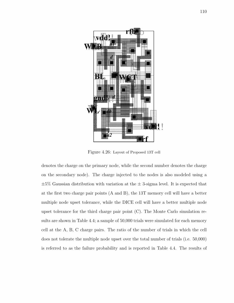
110
Figure 4.26: Layout of Proposed 13T cell
denotes the charge on the primary node, while the second number denotes the charge
on the secondary node). The charge injected to the nodes is also modeled using a
±5% Gaussian distribution with variation at the ± 3-sigma level. It is expected that
at the first two charge pair points (A and B), the 13T memory cell will have a better
multiple node upset tolerance, while the DICE cell will have a better multiple node
upset tolerance for the third charge pair point (C). The Monte Carlo simulation re-
sults are shown in Table 4.4; a sample of 50,000 trials were simulated for each memory
cell at the A, B, C charge pairs. The ratio of the number of trials in which the cell
does not tolerate the multiple node upset over the total number of trials (i.e. 50,000)
is referred to as the failure probability and is reported in Table 4.4. The results of

111
Table 4.4 confirms the robust multiple node upset tolerance of the hardened cells
in the presence of PVT variations, i.e. if in Figure 4.24 the charge pair is located
under the curve, then the presence of PVT variations does not affect its hardening
capability to tolerate a multiple node upset.
Table 4.4: Failure probability of memory cells with PVT variations
Memory Cell Num of tolerated tri-als (A: Q1=2.5fC,Q2=0.3fC)
Failure probability
DICE cell 19040/50000 61.92%11T cell 39250/50000 88.15%13T cell 50000/50000 0%
Memory Cell Num of tolerated tri-als (B: Q1=2.5fC,Q2=0.35fC)
Failure probability
DICE cell 12458/50000 75.08%11T cell 66/50000 99.87%13T cell 50000/50000 0%
Memory Cell Num of tolerated tri-als (C: Q1=2.2fC,Q2=0.5fC)
Failure probability
DICE cell 30099/50000 39.80%11T cell 0/50000 100%13T cell 0/50000 100%
4.10 Conclusion
This chapter has presented a few new designs for a highly stable hardened memory
cell in CMOS at 32nm feature size. First, a 14T hardened memory cell has been
proposed; the proposed new hardened memory cell relies on connecting a capacitor
to the storage node during the standby mode and disconnecting the capacitor during

112
the write operation. Two additional read access transistors are added to the cell to
overcome the stability problem encountered in [68]. As a high stability is achieved
by separating read and write operations, the transistors in the proposed hardened
memory cell can be resized to optimize power and performance. Simulation results
shows that the half pull-down transistor scaling (HP cell) is the best transistor sizing
for the proposed hardened memory cell at only a 7% increase in layout area. The
impact of process and temperature variations on the critical charge of the proposed
hardening cell has been analyzed. It has been shown that the proposed hardened cell is
very stable even in the presence of process and temperature variations. Consequently,
the proposed hardened memory cell is preferable when designing memories for both
high stability and performance.
Previous hardened designs like DICE cell incur in an increase of power consump-
tion and delay; yet another hardened design [47] suffers from two problems that result
in failure of its operation. In order to solve those problems in [47], the new config-
uration has been proposed, analyzed, and simulated using the predictive technology
model [52] for soft error hardening at 32nm technology node. The proposed radia-
tion hardened memory cell relies on a novel access mechanism along with two refresh
transistors; the proposed cell requires 11 transistors, i.e. one less than the DICE con-
figuration (hence incurring in a smaller overhead in layout and area). Moreover, the
proposed cell has been simulated, and assessed for critical charge, power consumption,
and delay to overcome the problems encountered in [47]. Using HSPICE, simulation
results have confirmed that the proposed memory cell accomplishes the highest soft
error tolerance through hardening (it has more than twice the critical charge than
the 6T unhardened configuration) and an impressive power-delay product compared
113
with the other hardened design commonly referred to as DICE.
Finally, this chapter has presented a model, analysis and assessment for hardening
a storage element (memory cell and latch) in the presence of a transient fault/soft
error resulting in a multiple node upset. The likely scenario of a double node upset
has been considered and a new memory cell has been proposed based on a novel
methodology. This methodology, whose correctness has been verified in [67] (yielding
similar results to 3D device simulation), relies on the so-called critical pair; the critical
pair allows establishing the plot of the primary node charge versus the secondary
charge such that the area under this curve defines the tolerance to a single event with
multiple node upsets for a hardened storage element. The proposed 13T cell utilizes
two additional transistors to the 11T design with a Schmitt trigger configuration to
increase the critical charge at the secondary node. Tolerance, power consumption, and
delay of this 13T design have been compared with existing hardened designs such as
DICE. Using HSPICE, simulation results have confirmed that the proposed memory
cell accomplishes the best multiple node upset tolerance, and impressive performance
(delay and power consumption) compared with previous hardened designs. Under a
single event with multiple node upsets, the simulation has established that the 13T cell
always outperforms the 11T cell. Compared with DICE, the proposed cell has better
tolerance provided that charge sharing is very diffused or limited (as encountered in
practical designs [3]). The superiority of the proposed design is also retained under
PVT variations.
Chapter 5
Analysis and Design of Soft ErrorHardened Latches
5.1 Introduction
Soft errors in memories (both static and dynamic) have traditionally been a much
greater concern than soft errors in combinational logic circuits (for the same minimum
feature size) since memories contain by far the largest number and density of bits
susceptible to particle strikes. In the next decade, technology trends – smaller feature
sizes, lower voltage levels, higher operating frequencies, and reduced logic depth – are
projected to cause an increase in the soft error failure rate in core combinational logic
in integrated circuits. Data latches are used in latch chains and as separate logic gates
for data manipulation and storage and must have a good tolerance to soft errors.
Many error tolerant methods for soft errors occurring in latches of logic circuits have
been proposed. The cost in terms of area, speed, and power for protecting memories
and latches from a TF can be significant. Therefore, data integrity against TFs is of
the utmost importance for general-purpose applications. For SEs due to TFs affecting
a sampling element, hardening has been proposed for low-cost robust design of latches
[44].
114
115
The objective of this chapter is to propose novel low power and higher soft error
tolerant designs for radiation hardening latch circuits in CMOS at the 32nm feature
size. By addressing the design issues in the initially proposed in [37] in more detail,
this paper presents the analysis of the novel features in detail and compares these
designs with existing hardened latch configurations found in the technical literature
[44] [63] [26] along with extensive simulations results. Tolerance to soft errors is
achieved due to a higher critical charge that is also complemented by higher perfor-
mance metrics such reduced area overhead. A metric (denoted as QPAR) to assess
hardening as well as design figures of merit (such as delay, area, and power) is intro-
duced to compare the proposed latches with existing configurations. Area efficiency
of the proposed latches is compared with the conventional hardening latches based on
actual layout. Extensive simulation results are used to assess and compare the effec-
tiveness of the new designs. It is shown that the proposed latches offer considerable
advantages at the 32nm feature size (using its predictive technology file) based on
QPAR. An assessment of the process variation impact is also provided using Monte
Carlo simulation. Finally, the multiple node upset scenario and previous analysis are
extended to harden latches as type of storage elements.
5.2 Soft Error Modeling
Figure 5.1 shows the soft error occurrence model of [77] used in the latch simulation.
In this figure, with no loss of generality and correctness, soft errors (resulting in a
signal glitch) occur at the inverter. The model on the left in Figure 5.1 shows the case
in which the normal output value for the inverter is high and soft errors occurring at
the NMOS transistor generate a negative pulse, whereas the one on the right shows
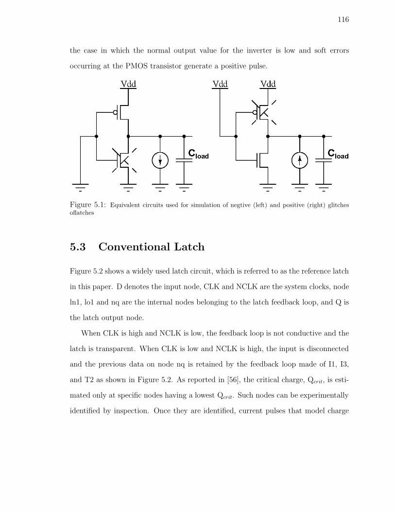
116
the case in which the normal output value for the inverter is low and soft errors
occurring at the PMOS transistor generate a positive pulse.
Figure 5.1: Equivalent circuits used for simulation of negtive (left) and positive (right) glitchesoflatches
5.3 Conventional Latch
Figure 5.2 shows a widely used latch circuit, which is referred to as the reference latch
in this paper. D denotes the input node, CLK and NCLK are the system clocks, node
ln1, lo1 and nq are the internal nodes belonging to the latch feedback loop, and Q is
the latch output node.
When CLK is high and NCLK is low, the feedback loop is not conductive and the
latch is transparent. When CLK is low and NCLK is high, the input is disconnected
and the previous data on node nq is retained by the feedback loop made of I1, I3,
and T2 as shown in Figure 5.2. As reported in [56], the critical charge, Qcrit, is esti-
mated only at specific nodes having a lowest Qcrit. Such nodes can be experimentally
identified by inspection. Once they are identified, current pulses that model charge

117
generation are applied to these nodes [77]. Experimental results show that the value
of Qcrit at node ln1 is the lowest among nodes ln1, nq, and lo1. Furthermore, this is
only one tenth of Qcrit of the other two nodes.
Figure 5.2: Reference (unhardened) latch
5.4 Existing Hardened Latches
The addition of gate capacitance to a critical node is one of the common methods
to harden CMOS devices. Hardened latch designs based on this approach have been
proposed in [44] and [63]. A soft error masking latch using Schmitt trigger circuit
(SEM-latch) has been proposed in [63]. Schmitt trigger has a larger hysteresis prop-
erty in voltage so that it can mask a transient pulse on the input. Meanwhile, it also
increases the critical charge of node ln1. As shown in Figure 5.3, transistors M1 and
M2 are added to the reference latch to make a Schmitt trigger. When CLK is high
and NCLK is low, the operation of the SEM-latch is the same as the reference latch
in Figure 5.2. When CLK is low and NCLK is high, transistors M1 and M2 make an
inverter in parallel with I1. The equivalent gate capacitance at node ln1 is increased,
thus also increasing the critical charge at node ln1.
A split internal node low-cost latch (SIN-LC latch) has been proposed in [44].
As shown in Figure 5.4, rather than adding node capacitance, the SIN-LC latch

118
Figure 5.3: A Schmitt trigger based hardening latch
utilizes an alternative feedback approach to harden the node. There are two inverter
stages from the input of the reference latch to the output in Figure 5.2. Therefore,
inverters I1 and I2 are added to the SIN-LC latch of [44] for a fair comparison with
the reference latch design. The feedback inverter of the SIN-LC latch is split into
two inverters I3 and I4. Nodes int2 and int1 (i.e. the outputs of inverters I3 and
I4) are connected to a series of transistors, M1-M3 and M2-M4. When CLK is low
and NCLK is high, the split feedback loop can correctly hold the data on node nq by
improving the critical charge at node nq. A transient pulse on node int1 or int2 will
not change the data as the serially connected transistors are separately driven by int2
and int1. Therefore, TFs on node int2 or int1 will only make the node nq to a high
impedance state without changing its logical value. Meanwhile, the critical charges
of the nodes int3 and int4 can be increased by sizing up M1 and M4, respectively. For
the SIN-LC latch, the node with the lowest critical charge is given by node nq. The
increase of the conductance of the transistors M1-M4 can also significantly increase
the critical charge of node nq. However, it affects the input-output delay worsening
its performance due to the conflicts between the transistors M1-M4 and the latch
input driver [44].
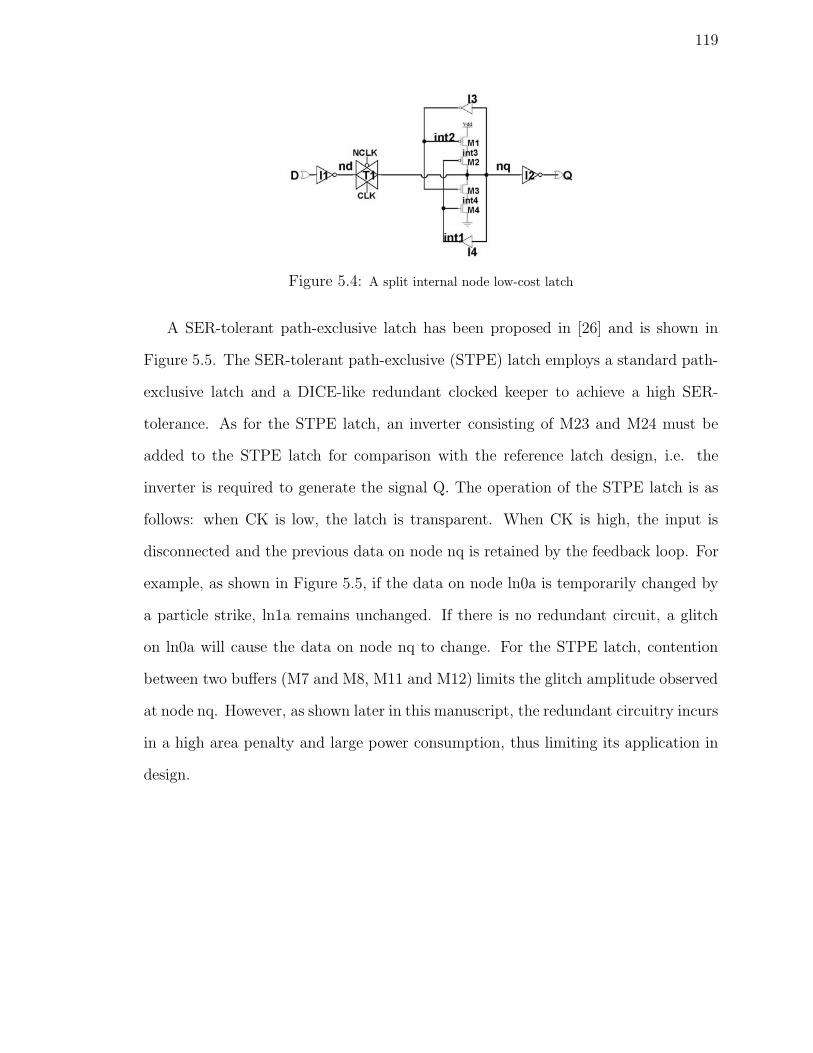
119
Figure 5.4: A split internal node low-cost latch
A SER-tolerant path-exclusive latch has been proposed in [26] and is shown in
Figure 5.5. The SER-tolerant path-exclusive (STPE) latch employs a standard path-
exclusive latch and a DICE-like redundant clocked keeper to achieve a high SER-
tolerance. As for the STPE latch, an inverter consisting of M23 and M24 must be
added to the STPE latch for comparison with the reference latch design, i.e. the
inverter is required to generate the signal Q. The operation of the STPE latch is as
follows: when CK is low, the latch is transparent. When CK is high, the input is
disconnected and the previous data on node nq is retained by the feedback loop. For
example, as shown in Figure 5.5, if the data on node ln0a is temporarily changed by
a particle strike, ln1a remains unchanged. If there is no redundant circuit, a glitch
on ln0a will cause the data on node nq to change. For the STPE latch, contention
between two buffers (M7 and M8, M11 and M12) limits the glitch amplitude observed
at node nq. However, as shown later in this manuscript, the redundant circuitry incurs
in a high area penalty and large power consumption, thus limiting its application in
design.

120
Figure 5.5: SER-tolerant path-exclusive latch
5.5 Proposed Hardened Latches
In this section, three new designs of hardened latches are proposed and analyzed.
5.5.1 Modified SEM-latch
The Schmitt trigger configuration used in the SEM-latch is shown in Figure 5.3.
This design can mask a transient pulse on the input node D when CLK is high
because the Schmitt trigger can suppress the glitches on the input. When CLK is
low, the additional transistors M1 and M2 provide a higher gate capacitance to slightly
increase the critical charge on node ln1. However, a TF will still propagate when a
larger transient pulse strikes the node ln1 and the positive feedback loop from M1
and M2 (together with inverter I1) amplifies the transient pulse. Thus, a TF causes a
SE on the latch. The SEM-latch provides little improvement to the critical charge on
node ln1. A modification of the SEM-latch design can, however, provide a significant
improvement in critical charge. This new design is shown in Figure 5.6, where the
positive feedback transistors M1 and M2 in Figure 5.3 are replaced by inverters I4,
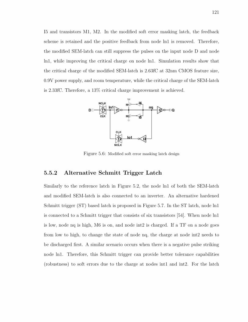
121
I5 and transistors M1, M2. In the modified soft error masking latch, the feedback
scheme is retained and the positive feedback from node ln1 is removed. Therefore,
the modified SEM-latch can still suppress the pulses on the input node D and node
ln1, while improving the critical charge on node ln1. Simulation results show that
the critical charge of the modified SEM-latch is 2.63fC at 32nm CMOS feature size,
0.9V power supply, and room temperature, while the critical charge of the SEM-latch
is 2.33fC. Therefore, a 13% critical charge improvement is achieved.
Figure 5.6: Modified soft error masking latch design
5.5.2 Alternative Schmitt Trigger Latch
Similarly to the reference latch in Figure 5.2, the node ln1 of both the SEM-latch
and modified SEM-latch is also connected to an inverter. An alternative hardened
Schmitt trigger (ST) based latch is proposed in Figure 5.7. In the ST latch, node ln1
is connected to a Schmitt trigger that consists of six transistors [54]. When node ln1
is low, node nq is high, M6 is on, and node int2 is charged. If a TF on a node goes
from low to high, to change the state of node nq, the charge at node int2 needs to
be discharged first. A similar scenario occurs when there is a negative pulse striking
node ln1. Therefore, this Schmitt trigger can provide better tolerance capabilities
(robustness) to soft errors due to the charge at nodes int1 and int2. For the latch

122
operation, when CLK is high and NCLK is low, the feedback loop is not conductive
and the latch is transparent. The proposed latch will be slower due to the hysteresis
property of the Schmitt trigger. When CLK is low and NCLK is high, the feedback
loop (that consists of the Schmitt trigger inverter and a normal inverter I2) retains
the data and the Schmitt trigger configuration provides better tolerance capabilities
(robustness) to soft errors.
Figure 5.7: Proposed Schmitt trigger based latch
5.5.3 Cascode Schmitt Trigger Latch
In the ST latch shown in Figure 5.7, the feedback loop consists of an inverter I2 and
a clock-controlled transmission gate T2. An alternative configuration of the feedback
loop is shown in Figure 5.8, in which both latches work exactly the same using a
digital cascade configuration. When the CLK is high and NCLK is low, the latch is
transparent, the feedback loop is on and the latch retains the data when the CLK is
low and NCLK is high.
However, the feedback configurations in Figure 5.7 and Figure 5.8 are different
from the operation of exiting the metastable state at the data-retaining phase. In a
hardened latch design, a maximum gain-bandwidth product of the positive feedback
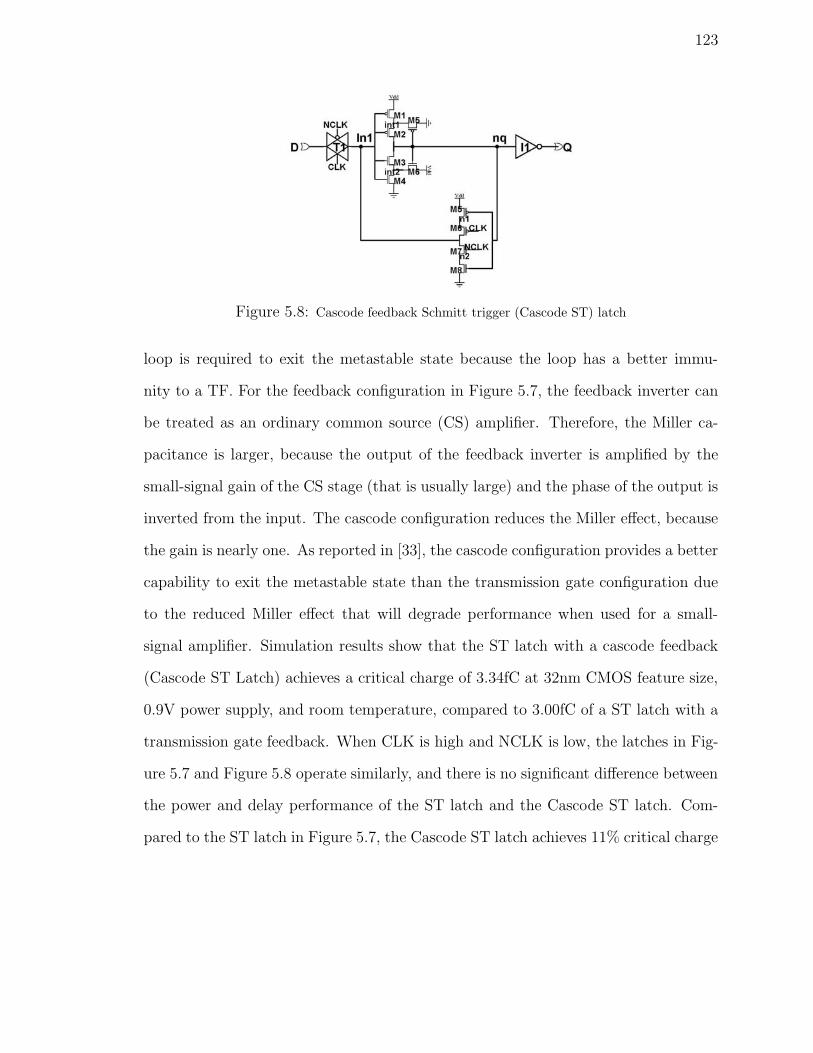
123
Figure 5.8: Cascode feedback Schmitt trigger (Cascode ST) latch
loop is required to exit the metastable state because the loop has a better immu-
nity to a TF. For the feedback configuration in Figure 5.7, the feedback inverter can
be treated as an ordinary common source (CS) amplifier. Therefore, the Miller ca-
pacitance is larger, because the output of the feedback inverter is amplified by the
small-signal gain of the CS stage (that is usually large) and the phase of the output is
inverted from the input. The cascode configuration reduces the Miller effect, because
the gain is nearly one. As reported in [33], the cascode configuration provides a better
capability to exit the metastable state than the transmission gate configuration due
to the reduced Miller effect that will degrade performance when used for a small-
signal amplifier. Simulation results show that the ST latch with a cascode feedback
(Cascode ST Latch) achieves a critical charge of 3.34fC at 32nm CMOS feature size,
0.9V power supply, and room temperature, compared to 3.00fC of a ST latch with a
transmission gate feedback. When CLK is high and NCLK is low, the latches in Fig-
ure 5.7 and Figure 5.8 operate similarly, and there is no significant difference between
the power and delay performance of the ST latch and the Cascode ST latch. Com-
pared to the ST latch in Figure 5.7, the Cascode ST latch achieves 11% critical charge
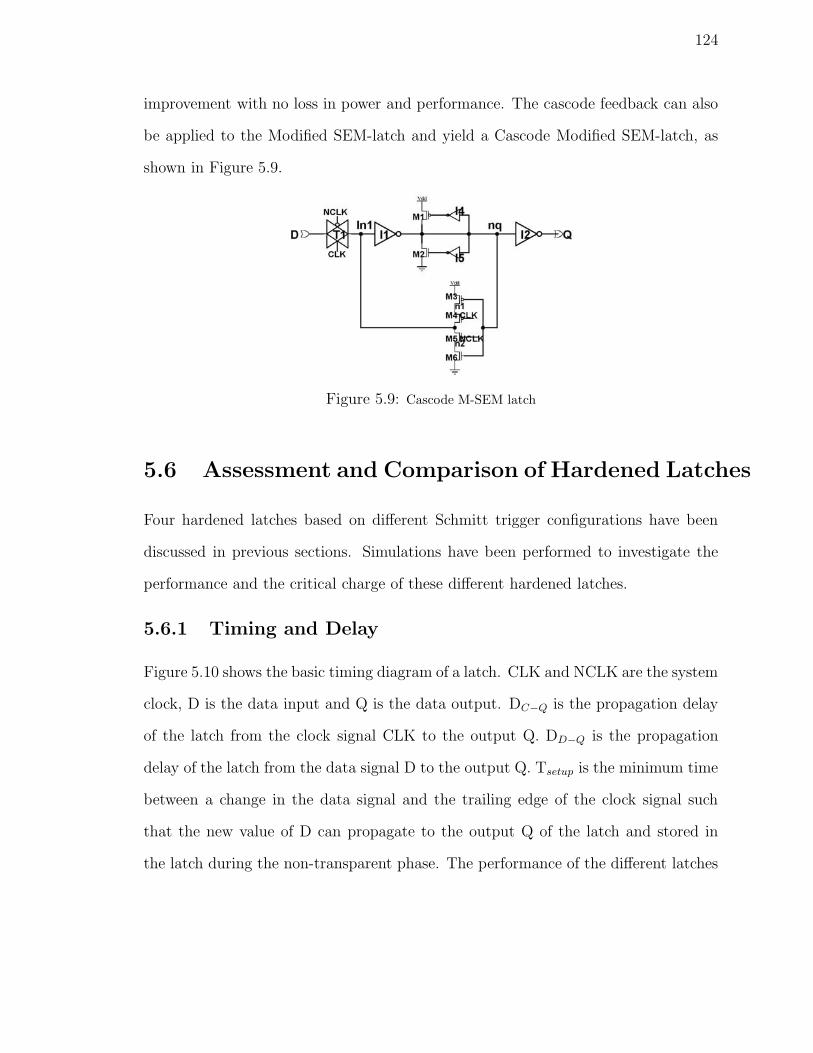
124
improvement with no loss in power and performance. The cascode feedback can also
be applied to the Modified SEM-latch and yield a Cascode Modified SEM-latch, as
shown in Figure 5.9.
Figure 5.9: Cascode M-SEM latch
5.6 Assessment and Comparison of Hardened Latches
Four hardened latches based on different Schmitt trigger configurations have been
discussed in previous sections. Simulations have been performed to investigate the
performance and the critical charge of these different hardened latches.
5.6.1 Timing and Delay
Figure 5.10 shows the basic timing diagram of a latch. CLK and NCLK are the system
clock, D is the data input and Q is the data output. DC−Q is the propagation delay
of the latch from the clock signal CLK to the output Q. DD−Q is the propagation
delay of the latch from the data signal D to the output Q. Tsetup is the minimum time
between a change in the data signal and the trailing edge of the clock signal such
that the new value of D can propagate to the output Q of the latch and stored in
the latch during the non-transparent phase. The performance of the different latches
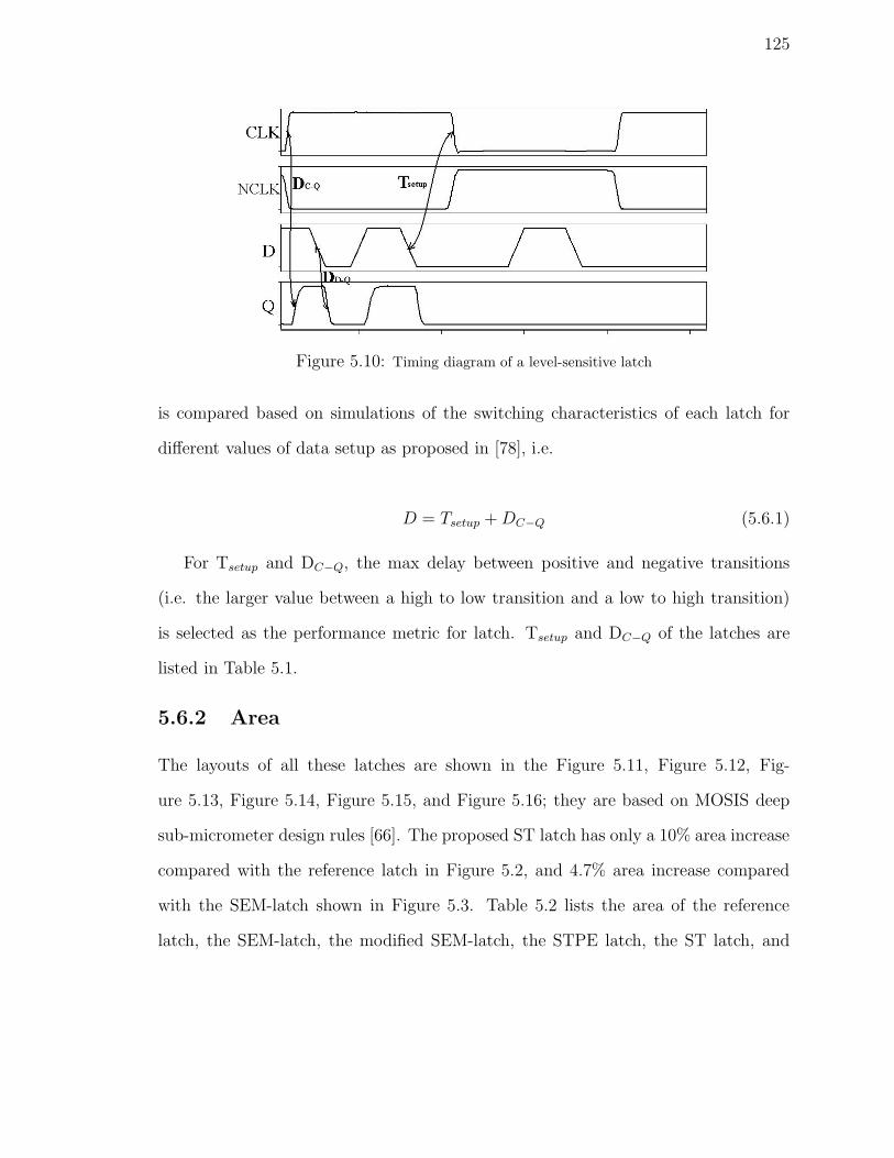
125
Figure 5.10: Timing diagram of a level-sensitive latch
is compared based on simulations of the switching characteristics of each latch for
different values of data setup as proposed in [78], i.e.
D = Tsetup +DC−Q (5.6.1)
For Tsetup and DC−Q, the max delay between positive and negative transitions
(i.e. the larger value between a high to low transition and a low to high transition)
is selected as the performance metric for latch. Tsetup and DC−Q of the latches are
listed in Table 5.1.
5.6.2 Area
The layouts of all these latches are shown in the Figure 5.11, Figure 5.12, Fig-
ure 5.13, Figure 5.14, Figure 5.15, and Figure 5.16; they are based on MOSIS deep
sub-micrometer design rules [66]. The proposed ST latch has only a 10% area increase
compared with the reference latch in Figure 5.2, and 4.7% area increase compared
with the SEM-latch shown in Figure 5.3. Table 5.2 lists the area of the reference
latch, the SEM-latch, the modified SEM-latch, the STPE latch, the ST latch, and
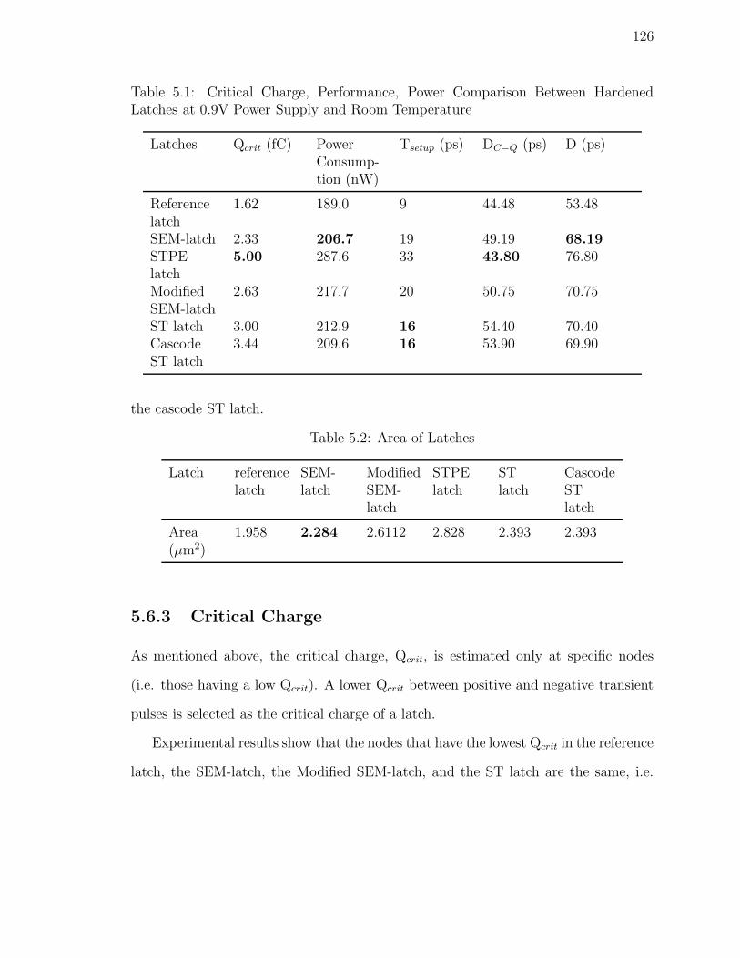
126
Table 5.1: Critical Charge, Performance, Power Comparison Between HardenedLatches at 0.9V Power Supply and Room Temperature
Latches Qcrit (fC) PowerConsump-tion (nW)
Tsetup (ps) DC−Q (ps) D (ps)
Referencelatch
1.62 189.0 9 44.48 53.48
SEM-latch 2.33 206.7 19 49.19 68.19STPElatch
5.00 287.6 33 43.80 76.80
ModifiedSEM-latch
2.63 217.7 20 50.75 70.75
ST latch 3.00 212.9 16 54.40 70.40CascodeST latch
3.44 209.6 16 53.90 69.90
the cascode ST latch.
Table 5.2: Area of Latches
Latch referencelatch
SEM-latch
ModifiedSEM-latch
STPElatch
STlatch
CascodeSTlatch
Area(μm2)
1.958 2.284 2.6112 2.828 2.393 2.393
5.6.3 Critical Charge
As mentioned above, the critical charge, Qcrit, is estimated only at specific nodes
(i.e. those having a low Qcrit). A lower Qcrit between positive and negative transient
pulses is selected as the critical charge of a latch.
Experimental results show that the nodes that have the lowest Qcrit in the reference
latch, the SEM-latch, the Modified SEM-latch, and the ST latch are the same, i.e.

127
Figure 5.11: Layout of reference latch
node ln1 in all circuits has the lowest Qcrit. Comparison of these six latches on critical
charge, performance, and power consumption is presented in Table 5.1. For fair
comparison, the transistor size of all the latches presented in this paper is equivalently
sized. All transistor size of SEM-latch and Modified SEM-latch are the same as that
of the reference latch. For ST latch and Cascode ST latch, the transmission gate T1
in Figure 5.7 and Figure 5.8 has been increased by 50% to drive two more transistors
connected to T1. Simulations have been performed on these four Schmitt trigger
based latches at 32nm CMOS feature size, 0.9V power supply, and room temperature.
Table 5.1 shows that by utilizing Schmitt trigger configuration, the critical charge of
the latch increases 43%, 62%, 85% and 112% for the SEM-latch, the Modified SEM-
latch, the ST latch, and the Cascode ST latch, respectively, while the delay and
power performance degrade at a smaller penalty. Simulations above are based on
using the predictive technology file at 32nm [52]. Simulations based on the netlists
extracted from layouts also confirm the critical charge improvement of the latches.
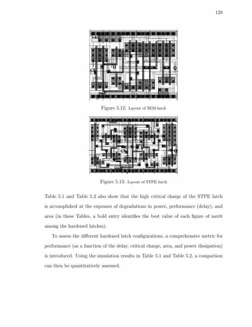
128
Figure 5.12: Layout of SEM-latch
Figure 5.13: Layout of STPE latch
Table 5.1 and Table 5.2 also show that the high critical charge of the STPE latch
is accomplished at the expenses of degradations in power, performance (delay), and
area (in these Tables, a bold entry identifies the best value of each figure of merit
among the hardened latches).
To assess the different hardened latch configurations, a comprehensive metric for
performance (as a function of the delay, critical charge, area, and power dissipation)
is introduced. Using the simulation results in Table 5.1 and Table 5.2, a comparison
can then be quantitatively assessed.
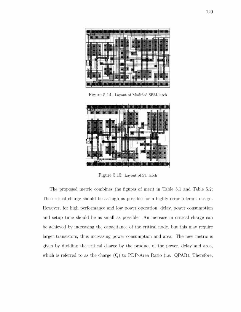
129
Figure 5.14: Layout of Modified SEM-latch
Figure 5.15: Layout of ST latch
The proposed metric combines the figures of merit in Table 5.1 and Table 5.2:
The critical charge should be as high as possible for a highly error-tolerant design.
However, for high performance and low power operation, delay, power consumption
and setup time should be as small as possible. An increase in critical charge can
be achieved by increasing the capacitance of the critical node, but this may require
larger transistors, thus increasing power consumption and area. The new metric is
given by dividing the critical charge by the product of the power, delay and area,
which is referred to as the charge (Q) to PDP-Area Ratio (i.e. QPAR). Therefore,

130
Figure 5.16: Layout of Cascode ST latch
the QPAR is given as follows:
QPAR =Critical Charge
Power × (Tsetup +DC−Q)× Area(5.6.2)
As in Eq. (5.6.2), a high value of QPAR corresponds to a high soft error tolerance,
high performance (low delay/compact area) and low power in hardened latches. The
QPARs of all the proposed and existing latch configurations are listed in Table 5.3.
Table 5.3 shows that the proposed Cascode ST latch has the highest QPAR, which is
36% higher than that of SEM-latch and 22% higher than that of STPE latch.
Table 5.3: QPAR of Latches
Latch referencelatch
SEM-latch
ModifiedSEM-latch
STPElatch
STlatch
CascodeSTlatch
QPAR 8.2e-5 7.2e-5 8e-5 6.5e-5 8.4e-5 9.8e-5
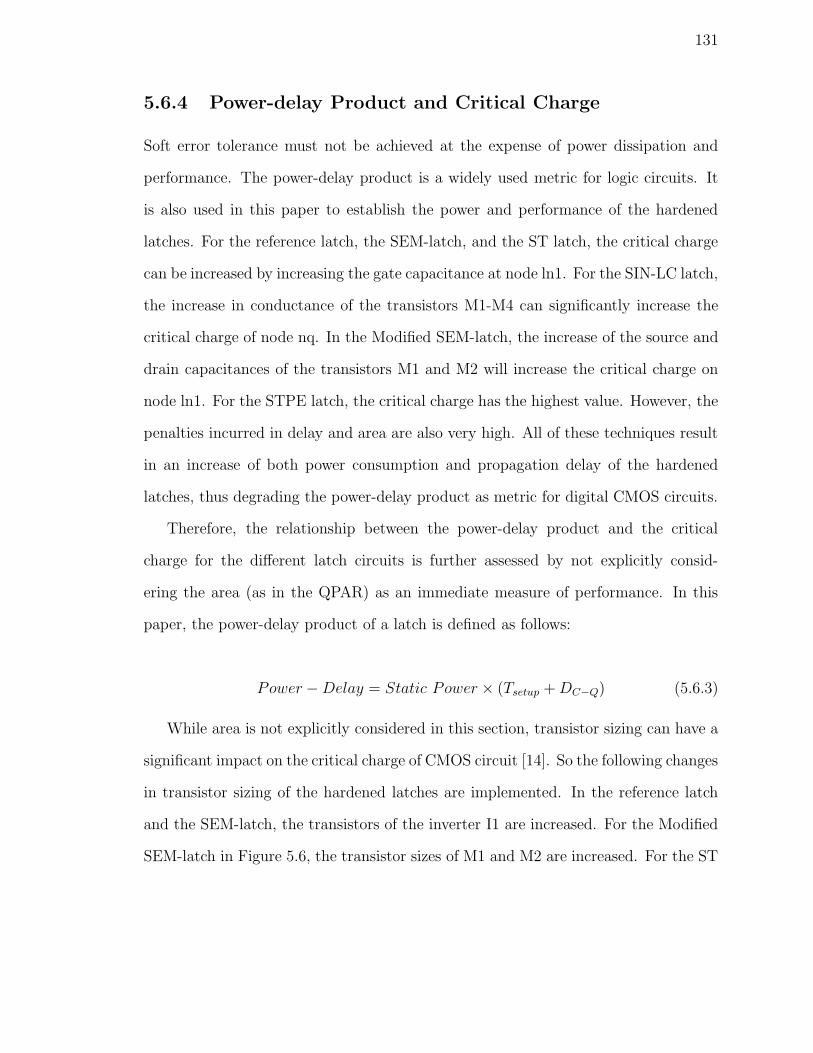
131
5.6.4 Power-delay Product and Critical Charge
Soft error tolerance must not be achieved at the expense of power dissipation and
performance. The power-delay product is a widely used metric for logic circuits. It
is also used in this paper to establish the power and performance of the hardened
latches. For the reference latch, the SEM-latch, and the ST latch, the critical charge
can be increased by increasing the gate capacitance at node ln1. For the SIN-LC latch,
the increase in conductance of the transistors M1-M4 can significantly increase the
critical charge of node nq. In the Modified SEM-latch, the increase of the source and
drain capacitances of the transistors M1 and M2 will increase the critical charge on
node ln1. For the STPE latch, the critical charge has the highest value. However, the
penalties incurred in delay and area are also very high. All of these techniques result
in an increase of both power consumption and propagation delay of the hardened
latches, thus degrading the power-delay product as metric for digital CMOS circuits.
Therefore, the relationship between the power-delay product and the critical
charge for the different latch circuits is further assessed by not explicitly consid-
ering the area (as in the QPAR) as an immediate measure of performance. In this
paper, the power-delay product of a latch is defined as follows:
Power−Delay = Static Power × (Tsetup +DC−Q) (5.6.3)
While area is not explicitly considered in this section, transistor sizing can have a
significant impact on the critical charge of CMOS circuit [14]. So the following changes
in transistor sizing of the hardened latches are implemented. In the reference latch
and the SEM-latch, the transistors of the inverter I1 are increased. For the Modified
SEM-latch in Figure 5.6, the transistor sizes of M1 and M2 are increased. For the ST
132
latch in Figure 5.7, an increase in sizing of the transistors M1-M4 is required. For
the SIN-LC latch, the transistors M1-M4 are also increased to have a higher critical
charge value at node nq. For the STPE latch in Figure 5.5, the transistors M7, M8,
M11, and M12 are increased for higher critical charge at node ln0a. Unfortunately
by utilizing an increase in gate sizing, the power-delay product will increase as well.
Figure 5.17 shows the relationship between the power-delay product and the critical
charge on the reference latch, the SEM-latch, the Modified SEM-latch, the SIN-LC
latch, ST latch, Cascode ST latch, and STPE latch. As shown in Figure 5.17, the
SEM-latch and the Modified SEM-latch utilize a parallel additional inverter to the
existing feedback loop during the non-transparent state, so they have a similar slope
in the plot. The ST latch, the Cascode ST latch, STPE latch, and the SIN-LC
latch achieve a significantly larger value of critical charge at a lower power-delay
product compared to the SEM-latch and the Modified SEM-latch. The STPE latch
has the highest critical charge at low values of power-delay product. However, as the
transistor sizes increase, the critical charge of the Cascode ST increases faster than
that of the STPE latch. As shown in Figure 5.17, the proposed Cascode ST latch has
the highest critical charge at higher values of power-delay product. Therefore, this
latch should be utilized in these cases for the highest soft error tolerance.
5.6.5 Process Variations
The effect of variations (process, voltage, and temperature) on soft error tolerance is
increasing with technology scaling. The soft error tolerance of the latches is also eval-
uated in the presence of process variations. In this section, Monte Carlo simulation
based on 10K samples is used for assessing the latch design under PVT variations. To
model PVT variations in the Monte Carlo simulations, parameters including voltage,
133
Figure 5.17: Plot of power-delay product vs. critical charge for different latch designs
temperature, and process (threshold voltage and channel length) are swept and sim-
ulations are run using a ±5% Gaussian distribution with variation at the ± 3-sigma
level. Table 5.4 shows the failure probability of hardening the original designs (whose
QPAR is given in Table 5.3) of the reference latch, the SEM latch, the Modified SEM
latch, the ST latch, the SIN-LC latch, the Cascode ST latch, and the STPE latch
when a fixed charge of 3fC is applied to the critical node of each latch. The results
of Table 5.4 confirm that as the induced charge is constant, then the probability of
failure of hardening is smaller when a larger Qcrit is present in the latch. However,
difference in the probability of failure between the Cascode ST and STPE latches is
negligible.
5.7 Multiple Node Upset Analysis
In this section, the multiple node upset scenario and previous analysis are extended
to harden latches as type of storage elements.

134
Table 5.4: Critical Charges and Failure Probability of Latches
Latch Critical Charge (fC) Hardening Failure Prob @ 3fC
reference latch 1.62 100%SEM-latch 2.33 100%Modified SEM-latch 2.63 97.76%ST latch 3.00 43.1%SIN-LC Latch 3.22 10.23%Cascode ST latch 3.34 0.41%STPE latch 5.00 0%
5.7.1 Multiple Node Upset Tolerance
As device scaling reduces the feature size, the multiple node upset is also becoming a
concern for latch design. The mode and analysis methodology presented in Chapter 4
for memory cells can also be applied to existing hardened latches to evaluate their
multiple node upset tolerance. As hardening is achieved by increasing the capacitance
of the critical node of the latch, higher the critical charge is, the better is the multiple
node tolerance of the latch. Similar to memory cells, critical pairs are indentified
first in the proposed hardening process. The primary nodes are the critical nodes
of the hardened latches, and HSPICE simulation has been performed on all single
node hardened latches to establish the secondary nodes. Simulation results show
that for SEM-latch, Modified SEM-latch, and ST latch, the critical pairs are always
the same, i.e. “ln11->0, lo1 1->0”. For the Modified SEM-latch and the ST latch, the
transmission gate feedback can be replaced by a cascode feedback, yielding a Cascode
Modified SEM-latch shown in Figure 5.9 and a Cascode ST latch shown in Figure 5.8.
For the Cascode Modified SEM-latch and the Cascode ST latch, the critical pairs are
“ln11->0, n2 1->0”, where node n2 is the internal node in the cascode feedback.
Similar to the multiple node upset scenario for memory cells, and after establishing

135
the critical pairs, the plot of primary node charge versus secondary node charge is
found by simulation [67] (Figure 5.18). As for the memory cells, larger the area under
the curve better is the tolerance to multiple node upsets. Figure 5.18 shows that the
curves intersect the X and Y axes, thus resulting in a single node charge upset (i.e.
when the charge deposited on the other node is 0). Table 5.1 shows that the cascode
configuration has higher critical charge than the transmission gate configuration for
both the M-SEM latch and the ST latch. However as shown in Figure 5.18 the
transmission gate configuration has a better tolerance to multiple node upsets (i.e. a
larger area under the curve). Take ST latch in Figure 5.7 and Cascode ST latch in
Figure 5.8 as an example. For the cascode configuration of Figure 5.8, the voltage on
node n2 is lower than Vdd, while in the transmission gate configuration of Figure 5.7,
the voltage on lo1 is Vdd. Moreover, the capacitance on node n2 of Figure 5.8 is
smaller than on node lo1 of Figure 5.7 (node n2 only has only two transistors on n2
and node lo1 has four transistors on the node). So, it is easier for the node n2 to
change its current state than node lo1. Hence, the transmission gate configuration
is preferable because it has better multiple node upset tolerance than the cascode
configuration.
5.7.2 Process Variation Impact on Multiple Node Upset Tol-
erance
The multiple node upset tolerance of the hardened latches is also evaluated in the
presence of PVT variations. To model PVT variations by Monte Carlo simulation,
the same conditions for the parameters (voltage, temperature, and process) as for
the memory cells are used. Two node charge pairs, marked as A (2.5fC, 0.5fC)
and B (2.2fC, 1.0fC), are selected for simulation because they are located between
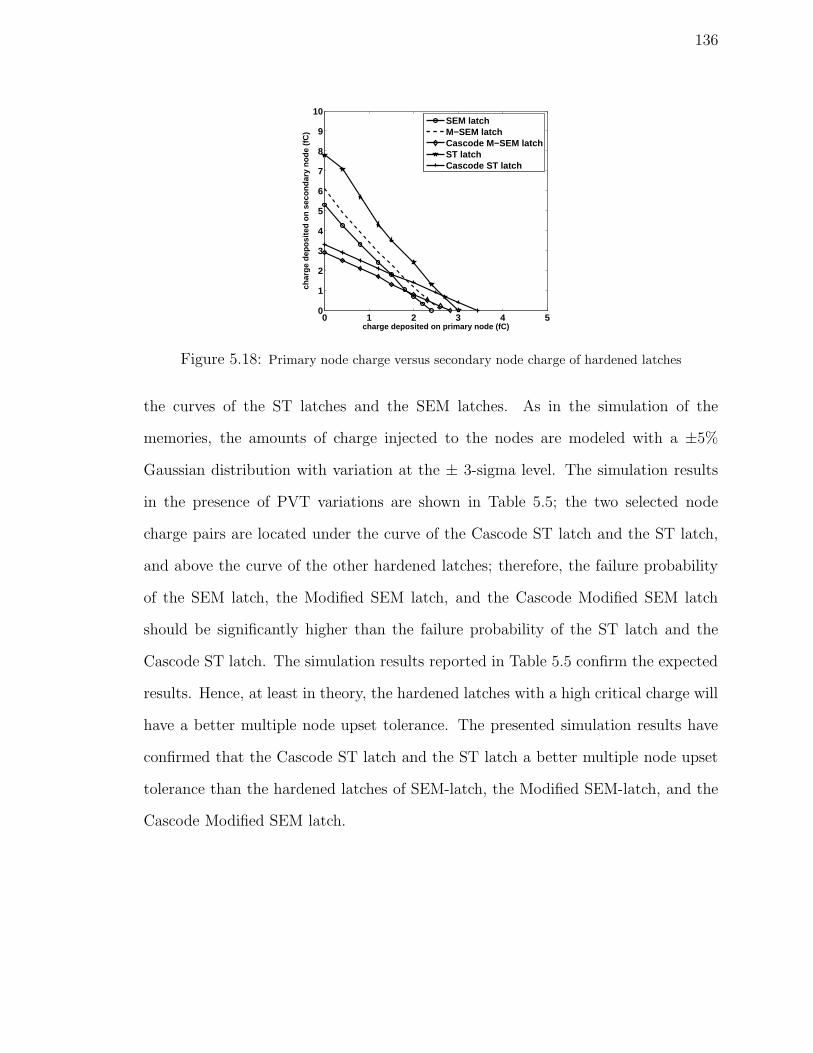
136
0 1 2 3 4 50
1
2
3
4
5
6
7
8
9
10
charge deposited on primary node (fC)
char
ge
dep
osi
ted
on
sec
on
dar
y n
od
e (f
C)
SEM latchM−SEM latchCascode M−SEM latchST latchCascode ST latch
Figure 5.18: Primary node charge versus secondary node charge of hardened latches
the curves of the ST latches and the SEM latches. As in the simulation of the
memories, the amounts of charge injected to the nodes are modeled with a ±5%
Gaussian distribution with variation at the ± 3-sigma level. The simulation results
in the presence of PVT variations are shown in Table 5.5; the two selected node
charge pairs are located under the curve of the Cascode ST latch and the ST latch,
and above the curve of the other hardened latches; therefore, the failure probability
of the SEM latch, the Modified SEM latch, and the Cascode Modified SEM latch
should be significantly higher than the failure probability of the ST latch and the
Cascode ST latch. The simulation results reported in Table 5.5 confirm the expected
results. Hence, at least in theory, the hardened latches with a high critical charge will
have a better multiple node upset tolerance. The presented simulation results have
confirmed that the Cascode ST latch and the ST latch a better multiple node upset
tolerance than the hardened latches of SEM-latch, the Modified SEM-latch, and the
Cascode Modified SEM latch.
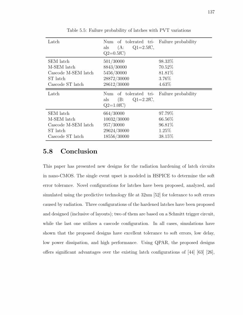
137
Table 5.5: Failure probability of latches with PVT variations
Latch Num of tolerated tri-als (A: Q1=2.5fC,Q2=0.5fC)
Failure probability
SEM latch 501/30000 98.33%M-SEM latch 8843/30000 70.52%Cascode M-SEM latch 5456/30000 81.81%ST latch 28872/30000 3.76%Cascode ST latch 28612/30000 4.63%
Latch Num of tolerated tri-als (B: Q1=2.2fC,Q2=1.0fC)
Failure probability
SEM latch 664/30000 97.79%M-SEM latch 10032/30000 66.56%Cascode M-SEM latch 957/30000 96.81%ST latch 29624/30000 1.25%Cascode ST latch 18556/30000 38.15%
5.8 Conclusion
This paper has presented new designs for the radiation hardening of latch circuits
in nano-CMOS. The single event upset is modeled in HSPICE to determine the soft
error tolerance. Novel configurations for latches have been proposed, analyzed, and
simulated using the predictive technology file at 32nm [52] for tolerance to soft errors
caused by radiation. Three configurations of the hardened latches have been proposed
and designed (inclusive of layouts); two of them are based on a Schmitt trigger circuit,
while the last one utilizes a cascode configuration. In all cases, simulations have
shown that the proposed designs have excellent tolerance to soft errors, low delay,
low power dissipation, and high performance. Using QPAR, the proposed designs
offers significant advantages over the existing latch configurations of [44] [63] [26],
138
and provide excellent performance at the reduced feature size of 32nm. The proposed
Cascode ST latch has the highest QPAR; Monte Carlo simulation has also been
performed under PVT variations. A multiple node upset analysis has also been
pursued for hardening latches; it has been shown that the hardened latch with the
highest critical charge has also the best tolerance for a multiple node upset.
Chapter 6
Summary and Future Works
6.1 Summary of Contributions
The objective of this work is to propose robust design approaches for storage elements
based on both nano-CMOS and CNTFET.
Chapter 2 presents a new 9T cell for low power consumption and high cell stability.
An optimal pull-down to access transistor ratio has been found by considering cell
stability and performance. Critical charge and the write-trip current are utilized
to determine the optimum pull-up to access transistor ratio. Along with transistor
sizing/scaling, an innovative bitline balancing scheme has been utilized to reduce the
leakage current at memory array-level. Hence in this proposed memory design, the
design is addressed at both cell and array levels. Simulation results have shown that
the proposed write scheme for the proposed 9T SRAM cell-based array achieves a
substantial reduction in power consumption at a typical process corner compared
with a conventional 6T SRAM cell based array. HSPICE simulation results confirm
that the proposed scheme achieves a 33% power saving compared to the conventional
SRAM array based on the 6T cell configuration. The simulation results have also
confirmed that the proposed cell is highly stable and resilient to process variations.
139
140
In Chapter 3, the use of CNTFETs in 6T SRAM design is investigated. A dual-
diameter CNTFET SRAM cell configuration with different threshold voltages is de-
signed, which is made possible by using different diameters for the P-type and N-type
CNTs in the cell. The best chirality for the PCNTFETs was selected to achieve high
stability, fast write time, and low power consumption. The proposed design shows
significant improvements compared to its CMOS counterpart in terms of power con-
sumption (44% less power consumption) and stability (75% higher static noise mar-
gin).
A new comprehensive metric for SRAM cells (denoted as SPR) has then been
proposed. SPR is a composite performance measure in terms of high stability, low
power and low delay. The proposed 9T SRAM cell in Chapter 2 has the best SPR
among all cell configurations found in the current literature. Simulation result shows
that the proposed 9T cell achieves 2.84 times higher than the conventional 6T cell.
The metric SPR has also been applied to the CNTFET SRAM cell and The pro-
posed dual-diameter CNTFET SRAM cell has a 3.82 times higher SPR under write
operation than its CMOS counterpart cell. SPR provides a composite and versatile
performance measure in terms of stability, power, and delay.
Hardening has been shown to be an effective way of increasing the single event up-
sets tolerance of memory cells with little impact on circuit density. The effectiveness
of the hardened cell is measured by critical charge. In Chapter 4, a 14T hardened
memory cell has been proposed. The proposed new hardened memory cell relies on
connecting a capacitor to the storage node during the standby mode and disconnect-
ing the capacitor during the write operation. By separating the circuitry for the write
and read operations, the static stability of the proposed cell configuration increase
141
more than 4.4 times compared to the conventional design. Simulation also shows
that by appropriately sizing the pull-down transistors, the proposed cell results in
a 40% higher critical charge and 13% less delay than the conventional design. An-
other hardening approach, where the feedback loop of the cell is blocked to keep the
transient pulse from propagating along the loop, is also proposed in this chapter. By
utilizing novel access and refreshing mechanisms, the data stored in the proposed 11T
hardened memory cell does not change even for a transient pulse of more than twice
the charge than a conventional memory cell, with a small cost in terms of power delay
product.
This dissertation has also presented a model, analysis and assessment for harden-
ing a memory cell in the presence of a transient fault/soft error resulting in a multiple
node upset. A 13T hardened memory cell utilizing Schmitt trigger configuration is
also proposed to improve multiple node upset tolerance of the hardened memory cell.
Using HSPICE, simulation results have confirmed that the proposed memory cell ac-
complishes the best multiple node upset tolerance, and impressive performance (delay
and power consumption) compared with previous hardened designs. Under a single
event with a multiple node upset, the simulation has established that the proposed
cell outperforms always the 11T cell. Compared with DICE, the proposed 13T cell has
better tolerance provided that charge sharing/collection is very diffused or limited.
The performance of the proposed design is also retained under PVT variations.
In combinational logic circuits, data latches are susceptible to single event upsets.
Therefore, the tolerance of the latch circuit to the soft errors is a strict requirement
in nanoscale circuit designs. Three new hardened designs for CMOS latches at 32nm
feature size are proposed in Chapter 5; two of these circuits are Schmitt trigger based,
142
while the third one utilizes a cascode configuration in the feedback loop. The cascode
ST latch has 112% higher critical charge than the conventional reference latch with
only 10% area increase. A novel design metric (QPAR) for latches is introduced to
assess the overall design effectiveness such as area, performance, power, and soft error
tolerance. The novel metric (QPAR) shows the proposed cascode ST latch achieves
up to 36% improvement in terms of QPAR compared with the existing hardening
designs. Finally, multiple node upset analysis has also been pursued for hardening
latches; additionally, it has shown that a cascode configuration has a higher critical
charge than a transmission gate configuration in both the M-SEM latch and the ST
latch. However, the transmission gate configuration has better multiple node upset
tolerance than the cascode configuration due to the larger node capacitance and the
higher voltage level at the secondary node.
6.2 Future Works
In this section we provide some directions for future research based on the material
presented throughout this dissertation.
6.2.1 Single Event Upset Tolerant Latch Design
All latches proposed in Chapter 5 belong to the first category of hardening approaches
mentioned in Chapter 4. In this category, hardening is achieved in the design by
increasing the capacitance of some nodes, or the strength of the transistors through
a novel design. Hardened design in this category is not totally insensitive to TFs.
Hardened latch design utilizing DICE configuration has been proposed in [26] and
[40], however, these designs require local redundancy therefore result in large area
143
and high power consumption. The feedback configuration shown in Figure 4.14 can
be also used to design a hardened latch, similar to the proposed 11T cell in Chapter 4.
By utilizing the feedback configuration shown in Figure 4.14, it is possible to design
a low cost single event upset tolerant latch.
6.2.2 CNTFET-based Hardened Design
Carbon nanotubes have attracted widespread attention of electron device and circuit
designers as possible channel material for high-performance transistors. Chapter 3
has shown a possible memory cell design with CNTFET and high static stability
has been achieved with dual-chirality selection. As carbon nanotubes are also grown
on the silicon substrate in the CNTFETs, the cosmic ray neutrons and α-particles
may also cause voltage change on the drain and source of the CNTFETs. Therefore,
it would be interesting to investigate the soft error mechanisms on CNTFET-based
design and propose CNTFET-based hardened storage elements. Moreover, a novel
CNT-based device, Complementary Nano Electro-Mechanical Switch (CNEMS) has
been proposed in [15] and storage elements designed using CNEMS are immume to
soft errors. It would be an interesting topic for robust storage elements design if there
is accurate simulation model available.

Bibliography
[1] A. Agarwal, S. Mukhopadhyay, A. Raychowdhury, K. Roy, and C.H. Kim, Leak-
age power analysis and reduction for nanoscale circuits, IEEE Micro 26 (2006),
no. 2, 68–80.
[2] A. Akturk, G. Pennington, N. Goldsman, and A. Wickenden, Electron transport
and velocity oscillations in a carbon nanotube, IEEE Transactions on Nanotech-
nology 6 (2007), no. 4, 469–474.
[3] G.A. Amusan, I.W. Massengill, M.P. Baze, A.L. Sternberg, A. Witulski, B.I.
Bhuva, and J.D. Black, Single event upsets in deep submicrometer technologies
due to charge sharing, IEEE Transactions on Device and Materials Reliability 8
(2008), no. 3, 582–589.
[4] G.A. Amusan, A. Witulski, I.W. Massengill, B.I. Bhuva, P.R. Fleming, M.L.
Alles, A.L. Sternberg, and J.D. Black, Charge collection and charge sharing in
a 130 nm cmos technology, IEEE Transactions on Nuclear Science 53 (2006),
no. 6, 3253–3258.
[5] J. Appenzeller, Carbon nanotubes for high-performance electronicsprogress and
prospect, IEEE 96 (2008), no. 2, 201–211.
[6] A. Bachtold, P. Hadley, T. Nakanishi, and C. Dekker, Logic circuits with carbon
nanotube transistors, Science 294 (2001), no. 5545, 1317–1320.
144

145
[7] R. Baumann, Soft errors in advanced computer systems, IEEE Design and Test
of Computers 22 (2005), no. 3, 258–266.
[8] B.H. Calhoun and A.P. Chandrakasan, A 256-kb 65-nm sub-threshold sram design
for ultra-low-voltage operation, IEEE Journal of Solid-State Circuits 42 (2007),
no. 3, 680–688.
[9] A. Bhavnagarwala, S. Kosonocky, C. Radens, K. Stawiasz, R. Mann, Q. Ye, and
K. Chin, Fluctuation limits and scaling opportunities for cmos sram cells, IEEE
International Electron Device Meeting, 2005, pp. 659–662.
[10] D. R. Blum and J.G. Delgado-Frias, Hardened by design techniques for imple-
menting multiple-bit upset tolerant static memories, IEEE International Sympo-
sium on Circuits and Systems, 2007, pp. 2786–2789.
[11] B.H. Calhoun, Yu Cao, Xin Li, Ken Mai, L.T. Pileggi, R.A. Rutenbar, and
K.L. Shepard, Digital circuit design challenges and opportunities in the era of
nanoscale cmos, IEEE 96 (2008), no. 2, 343–365.
[12] B.H. Calhoun and A.P. Chandrakasan, Static noise margin variation for sub-
threshold sram in 65-nm cmos, IEEE Journal of Solid-State Circuits 41 (2006),
no. 7, 1673–1679.
[13] T. Calin, M. Nicolaidis, and R. Velazco, Upset hardened memory design for
submicron cmos technology, IEEE Transactions on Nuclear Science 43 (1996),
no. 6, 2874–2878.
[14] J.M. Cazeaux, D. Rossi, M. Omana, and C. Metra, On transistor level gate sizing
for increased robustness to transient faults, IEEE International On-Line Testing
Symposium, 2005, pp. 23–28.
146
[15] R. Chakraborty, S. Narasimhan, and S. Bhunia, Hybridization of cmos with cnt-
based nano-electromechanical switch for low leakage and robust circuit design,
IEEE Transactions on Circuits and Systems-I 54 (2007), no. 11, 2480–2488.
[16] A. Chandrakasan, W.J. Bowhill, and F. Fox, Design of high-performance micro-
processor circuits, IEEE Press, New Jersey, 2000.
[17] L. Chang, D.M. Fried, J. Hergenrother, J.W. Sleight, R. H. Dennard, R.K. Mon-
toye, L. Sekaric, S.J. McNab, A.W. Topol, C.D. Adams, K.W. Guarini, and
W. Haensch, Stable sram cell design for the 32 nm node and beyond, IEEE Sym-
posium on VLSI Technology, 2005, pp. 172–175.
[18] J. Deng and H.-S.P. Wong, A compact spice model for carbon-nanotube field-effect
transistors including nonidealities and its applicationpart i: Model of the intrinsic
channel region, IEEE transcations on Electron Devices 54 (2007), no. 12, 3186–
3194.
[19] C. Detcheverry, C. Dachs, E. Lorfevre, C. Sudre, G. Bruguier, J.M. Palau,
J. Gasiot, and E. Ecoffet, Seu critical charge and sensitive area in a submi-
cron cmos technology, IEEE Transactions on Nuclear Science 44 (1997), no. 6,
2266–2273.
[20] P.E. Dodd and L.W. Massengill, Basic mechanisms and modeling of single-
event upset in digital microelectronics, IEEE Transactions on Nuclear Science
50 (2003), no. 3, 583–602.
[21] K. Furutani, K. Arimoto, H. Miyamoto, T. Kobayashi, K. Yasuda, and
K. Mashiko, A built-in hamming code ecc circuit for drams, ieee journal of solid-
state circuits, IEEE Journal of Solid-State Circuits 24 (1989), no. 1, 50–56.
147
[22] E. Grossar, M. Stucchi, K. Maex, and W. Dehaene, Read stability and write-
ability analysis of sram cells for nanometer technologies, IEEE Journal of Solid-
State Circuits 41 (2006), no. 11, 2577–2588.
[23] Z. Guo, S. Balasubramanian, R. Zlatanovici, T.-J. King, and B. Nikolic, Finfet-
based sram design, IEEE International Symposium on Low Power Electronic
Design, 2005, pp. 2–7.
[24] T. Haraszti, Cmos memory circuits, Kluwer Academic Pub, Boston, 2000.
[25] H. Hashempour and F. Lombardi, Device model for ballistic cnfets using the first
conducting band, IEEE Design and Test of Computers 25 (2008), no. 2, 178–186.
[26] P. Hazucha, T. Karnik, S. Walstra, B.A. Bloechel, J.W. Tschanz, J. Maiz,
K. Soumyanath, G.E. Dermer, S. Narendra, and S. Borkar V. De, Measure-
ments and analysis of ser-tolerant latch in a 90-nm dual-vt cmos process, IEEE
Journal of Solid-State Circuits 39 (2004), no. 9, 1536–1543.
[27] P. Hazucha and C. Svensson, Impact of cmos technology scaling on the atmo-
spheric neutron soft error rate, IEEE Transactions on Nuclear Science 47 (2000),
no. 6, 2586–2594.
[28] M. Horowitz, E. Alon, D. Patil, S. Naffziger, K. Rajesh, and K. Bernstein, Scal-
ing, power, and the future of cmos, IEEE International Electron Device Meeting,
Technical Digest, 2005, pp. 7–15.
[29] K. Itoh, M. Horiguchi, and T. Kawahara, Ultra-low voltage nano-scale embedded
rams, IEEE International Symposium on Circuits and Systems, 2006, pp. 245–
248.
[30] J. Deng and H.-S.P. Wong, A compact spice model for carbon-nanotube field-
effect transistors including nonidealities and its applicationpart ii: Full device

148
model and circuit performance benchmarking, IEEE Transactions on Electron
Devices 54 (2007), no. 12, 3195–3205.
[31] S.M. Jahinuzzaman, M. Sharifkhani, and M. Sachdev, Investigation of process
impact on soft error susceptibility of nanometric srams using a compact criti-
cal charge model, IEEE International Symposium on Quality Electronic Design,
2008, pp. 207–212.
[32] R. Joshi, R. Houle, K. Batson, D. Rodko, P. Patel, W. Huott, R. Franch,
Y. Chan, D. Plass, S. Wilson, and P. Wang, 6.6+ ghz low vmin, read and
half select disturb-free 1.2 mb sram, IEEE Symposium on VLSI Circuits, 2007,
pp. 250–251.
[33] L.-S. Kim and R.W. Dutton, Metastability of cmos latch/flip-flop, IEEE Journal
of Solid-State Circuits 25 (1990), no. 4, 942–951.
[34] T. Kim, J. Liu, J. Keane, and C.H. Kim, A high-density subthreshold sram with
data-independent bitline leakage and virtual ground replica scheme, IEEE Inter-
national Solid-State Circuits Conference, 2007, pp. 330–331.
[35] J.P. Kulkarni, K. Kim, and K. Roy, A 160 mv robust schmitt trigger based sub-
threshold sram, IEEE Journal of Solid-State Circuits 42 (2007), no. 10, 2303–
2313.
[36] Y. Li, W. Kim, Y. Zhang, M. Rolandi, and D. Wang, Growth of single-walled car-
bon nanotubes from discrete catalytic nanoparticles of various sizes, The Journal
of Physical Chemistry 105 (2001), 11 424.
[37] S. Lin, Y.B. Kim, and F.Lombardi, Soft error hardening designs of nanoscale
cmos latches, IEEE VLSI Test Symposium, 2009, pp. 41–46.
[38] S. Lin, Y.B. Kim, and F. Lombardi, A low leakage 9t sram cell for ultra-low
power operation, ACM Great Lakes Symposium on VLSI, 2008, pp. 123–126.

149
[39] S. Lin, Y.B. Kim, F. Lombardi, and Y.J. Lee, A new sram cell design using
cntfets, IEEE International SoC Conference, 2008, pp. 168–171.
[40] S. Lin, H. Yang, and R. Luo, A new family of sequential elements with built-in
soft error tolerance for dual-vdd systems, IEEE Transactions on VLSI Systems
16 (2008), no. 10, 1372–1384.
[41] S. Lin, Y.B. Kim, and F. Lombardi, A novel design technique for soft error
hardening of a nanoscale cmos memory, IEEE Midwest Symposium on Circuits
and Systems, 2009, pp. 679–682.
[42] Y. Lin, J. Appenzeller, J. Knoch, and P. Avouris, High-performance carbon nan-
otube field-effect transistor with tunable polarities, IEEE Transactions on Nan-
otechnology 4 (2005), no. 5, 481–489.
[43] Z. Liu and V. Kursun, High read stability and low leakage cache memory cell,
IEEE International Symposium on Circuits and Systems, 2007, pp. 2774–2777.
[44] M. Omana, D. Rossi, and C. Metra, Latch susceptibility to transient faults and
new hardening approach, IEEE Transactions on Computers 56 (2007), no. 9,
1255–1268.
[45] J. Maiz, S. Hareland, K. Zhang, and P. Armstrong, Characterization of multi-bit
soft error events in advanced srams, IEEE International Electron Device Meeting,
Technical Digest, 2003, pp. 21.4.1–21.4.4.
[46] Y. Morita, H. Fujiwara, H. Noguchi, K. Kawakami, J. Miyakoshi, S. Mikami,
K. Nii, H. Kawaguchi, and M. Yoshimoto, A vth-variation-tolerant sram with
0.3-v minimum peration voltage for memory-rich soc under dvs environment,
IEEE Symposium on VLSI Circuits, 2006, pp. 13–14.
150
[47] M. Nicolaidis, R. Perez, and D. Alexandrescu, Low-cost highly-robust hardened
cells using blocking feedback transistors, IEEE VLSI Test Symposium, 2008,
pp. 371–376.
[48] H. Noguchi, S. Okumura, Y. Iguchi, H. Fujiwara, Y. Morita, K. Nii,
H. Kawaguchi, and M. Yoshimoto, Which is the best dual-port sram in 45-nm
process technology? 8t, 10t single end, and 10t differential, IEEE International
Conference on Integrated Circuit Design and Technology and Tutorial, 2008,
pp. 55–58.
[49] Y. Ohno, S. Kishimoto, T. Mizutani, T. Okazaki, and H. Shinohara, Chirality
assignment of individual single-walled carbon nanotubes in carbon nanotube field-
effect transistors by micro-photocurrent spectroscopy, Applied Physics Letters 84
(2004), no. 8, 1368–1370.
[50] M. Omana, D. Rossi, and C. Metra, Novel transient fault hardened static latch,
International Test Conference, 2003, pp. 886–892.
[51] B.C. Paul, S. Fujita, M. Okajima, T.H. Lee, H.-S.P. Wong, and Y. Nishi, Im-
pact of a process variation on nanowire and nanotube device performance, IEEE
Transactions on Electron Devices 54 (2007), no. 9, 2369–2376.
[52] Berkeley predictive technology model website, http://www.eas.asu.edu/
~ptm/.
[53] R. Baumann, Soft errors in advanced semiconductor devices-part i: the three ra-
diation sources, IEEE Transactions on Device and Materials Reliability 5 (2005),
no. 3, 305–316.
[54] J. Rabaey, A. Chandrakasan, and B. Nikolic, Digital integrated circuits:a design
perspective, Prentice Hall, New Jersey, 2002.
151
[55] A. Rahman, J. Guo, S. Datta, and M.S. Lundstrom, Theory of ballistic nanotran-
sistors, IEEE transcations on Electron Devices 50 (2003), no. 10, 1853–1864.
[56] R. Ramanarayanan, V. Degalahal, N. Vijaykrishnan, M.J. Irwin, and D. Duarte,
Analysis of soft error rate in flip-flops and scannable latches, IEEE International
SOC Conference, 2003, pp. 231–234.
[57] A. Raychowdhury and K. Roy, Carbon-nanotube-based voltage-mode multiple-
valued logic design, IEEE Transactions on Nanotechnology 4 (2005), no. 5, 481–
489.
[58] F. Ricci, L. T. Clark, T. Beatty, W. Yu, A. Bashmakov, S. Demmons, E. Fox,
J. Miller, M. Biyani, and J.Haigh, A 1.5 ghz 90 nm embedded microprocessor
core, IEEE Symposium on VLSI Technology, 2005, pp. 12–15.
[59] P. Roche and G.Gasiot, Impacts of front-end and middle-end process modifica-
tions on terrestrial soft error rate, IEEE Transactions on Device and Materials
Reliability 5 (2005), no. 3, 382–396.
[60] K. Roy, S. Mukhopadhyay, and H. Mahmoodi-Meimand, Leakage current mech-
anisms and leakage reduction techniques in deep-submicrometer cmos circuits,
IEEE 91 (2003), no. 2, 305–327.
[61] S. Lin, Y. B Kim, and F. Lombardi, Design of a cntfet-based sram cell by dual-
chirality selection, IEEE Transactions on Nanotechnology 9 (2010), no. 1, 30–37.
[62] S. Lin, Y.B. Kim, and F. Lombardi, A 32nm sram design for low power and high
stability, IEEE Midwest Symposium on Circuits and Systems, 2008, pp. 422–425.
[63] Y. Sasaki, K. Namba, and H. Ito, Soft error masking circuit and latch using
schmitt trigger circuit, IEEE International Symposium on Defect and Fault Tol-
erance in VLSI Systems, 2006, pp. 327–335.
152
[64] E. Seevinck, F.J. List, and J. Lohstroh, Static-noise margin analysis of mos sram
cells, IEEE Journal of Solid-State Circuits 22 (1987), no. 5, 748–754.
[65] N. Seifert, X. Zhu, and L.W. Massengill, Impact of scaling on soft-error rates in
commercial microprocessors, IEEE Transactions on Nuclear Science 49 (2002),
no. 6, 3100–3106.
[66] The MOSIS service, http://www.mosis.org/Technical/Designrules/scmos/
scmos-main.html.
[67] V. B. Sheshadri, B. L. Bhuva, R. A. Reed, R. A. Weller, M. H. Mendenhall, R. D.
Schrimpf, K. M. Warren, B. D. Sierawski, Shi-Jie Wen, and R. Wong, Effects
of multi-node charge collection in flip-flop designs at advanced technology nodes,
IEEE International Reliability Physics Symposium, 2010, pp. 1026–1030.
[68] Y. Shiyanovskii, F. Wolff, and C. Papachristou, Sram cell design protected from
seu upsets, IEEE International On-Line Testing Symposium, 2008, pp. 169–170.
[69] S.A. Tawfik, Z. Liu, and V. Kursun, Independent-gate and tied-gate finfet sram
circuits: Design guidelines for reduced area and enhanced stability, Internatonal
Conference on Microelectronics, 2007, pp. 171–174.
[70] R.F. Tsui, J.R. Shih, K. Liu, Y.S. Tsai, H.W. Chin, and K. Wu, Reliability
assessment of the embedded dram technology with pmosfet transfer transistor
and high-k dielectrics (ta2o5) mim capacitor, IEEE International Symposium on
VLSI Technology, Systems, and Applications, 2006, pp. 1–2.
[71] C-C. Wang, C-F. Wu, R-T. Hwang, and C-H. Kao, Single-ended sram with high
test coverage and short test time, IEEE Journal of Solid-State Circuits 35 (2000),
no. 1, 114–118.
153
[72] W. Wang and H. Gong, Edge triggered pulse latch design with delayed latching
edge for radiation hardened application, IEEE Transactions on Nuclear Science
51 (2004), no. 6, 3626–3630.
[73] C. Wann, R. Wong, D.J. Frank, R. Mann, Shang-Bin Ko, P. Croce, D. Lea,
D. Hoyniak, Yoo-Mi Lee, J. Toomey, M. Weybright, and J. Sudijono, Sram
cell design for stability methodology, IEEE International Symposium on VLSI
Technology, Systems and Applications, 2005, pp. 21–22.
[74] Stanford University CNFET Model website, http://nano.stanford.edu/
model.php?id=23.
[75] W. Wolf, Modern vlsi design: System-on-chip design, Prentice Hall, New Jersey,
2002.
[76] K.-C. Wu and D. Marculescu, Soft error rate reduction using redundancy addi-
tion and removal, Asia and South Pacific Design Automation Conference, 2008,
pp. 559–564.
[77] F.L. Yang and R.A. Saleh, Simulation and analysis of transient faults in digital
circuits, IEEE Journal of Solid-State Circuits 27 (1992), no. 3, 258–264.
[78] V. Zyuban, Optimization of scannable latches for low energy, IEEE Transactions
on Very Large Scale Integration Systems 11 (2003), no. 5, 778–788.


![EnergyEfficiencyAdaptationforMultihopRoutingin ...downloads.hindawi.com/journals/jcnc/2012/767920.pdfnetwork,wetakeintoconsiderationthehardware(orcircuit) energy consumption [8]](https://img.dokumen.tips/doc/110x75/5ac842097f8b9a40728c98d9/energyefciencyadaptationformultihoproutingin-wetakeintoconsiderationthehardwareorcircuit.jpg)


![1374 bae[1]](https://img.dokumen.tips/doc/110x75/5590c45a1a28ab9d718b45d3/1374-bae1.jpg)