Embed Size (px)
Citation preview
Plasma Sources Science and Technology
Plasma Sources Sci. Technol. 23 (2014) 015006 (13pp) doi:10.1088/0963-0252/23/1/015006
Analysis of resonant planar dissipativenetwork antennas for rf inductively coupledplasma sources
Ph Guittienne1, A A Howling2 and Ch Hollenstein2
1 Helyssen, Route de la Louche 31, CH-1092 Belmont-sur-Lausanne, Switzerland2 Ecole Polytechnique Federale de Lausanne (EPFL), Centre de Recherches en Physique des Plasmas,CH-1015 Lausanne, Switzerland
Received 1 July 2013, revised 5 November 2013Accepted for publication 25 November 2013Published 10 January 2014
AbstractThe analysis of a radio-frequency (RF) planar antenna is presented for applications in plasmaprocessing. The antenna is a network of elementary meshes composed of inductive andcapacitive elements which exhibits a set of resonant modes. The high currents generated byRF power feeding under resonance are efficient for plasma generation. A general solution isderived for the currents in the driven dissipative network for these conditions. The dominantlyreal input impedance near antenna resonance avoids the high reactive currents and voltages inthe matching box and RF power connections which can be a problem with conventionallarge-area capacitively and inductively coupled plasma sources. The driven antenna can beapproximated by a parallel resonance equivalent circuit whose input impedance canconveniently be measured to interpret the dissipation due to the plasma.
1. Introduction
Plasmas are used for various applications such as solar cellproduction, semiconductor manufacturing, food packagingand space propulsion, to name just a few. There is a constantneed to improve plasma sources in order to increase the processrates and to develop new types of products. One aspect ofsource performance is the requirement of high electron density,since a dense plasma generally leads to high dissociation ratesand an efficient use of the process precursors. A secondimportant aspect lies in the possibility of large-area plasmaprocessing. This has a double interest as it would allow largeramounts of small pieces to be treated in a single run as well aslarger work-pieces to be processed.
Radio-frequency (RF) driven discharges are commonlyused for high density plasma sources [1]. Considerabledifficulties are often met in the generation of very large-area plasma with regard to the RF power injection, becauseconventional RF sources present almost purely reactiveinput impedance which tends either towards zero (capacitivedischarges) or towards infinity (inductive discharges) withincreasing area. The impedance matching between the RFgenerator and the source then drives very high currents and/orvoltages in the matching network and power feed lines.
These limitations could be overcome using RF networkantennas (Helyssen sources) whose essential characteristicis that they are resonant devices. When excited at one ofits resonance frequencies the antenna develops very highcurrents within its structure, which can be used for inductivelycoupled plasma sources [2–4]. These resonating currentdistributions are called the normal modes of the antenna and arecharacterized by their sinusoidal distribution [5]. In additionto the fact that the high current distributions generated atresonance are very efficient in terms of plasma generation, amajor advantage of these antennas lies in their input impedanceproperties which could allow very large-area plasma sources tobe developed. In its cylindrical version (closed configuration),the Helyssen antenna was shown to be well-adapted for plasmageneration by helicon wave excitation in the presence of a staticmagnetic field [6].
A planar version of a resonant antenna was recentlyconstructed and showed good performance in terms of plasmauniformity and high electron density [2–4]. Measurements ofthe antenna impedance [2] showed that it behaved as a parallelresonance circuit in the neighborhood of a resonant mode. Adissipative network model is developed here to interpret thosemeasurements in terms of the effect of plasma coupling onthe antenna component values. This model also provides a
0963-0252/14/015006+13$33.00 1 © 2014 IOP Publishing Ltd Printed in the UK
Plasma Sources Sci. Technol. 23 (2014) 015006 Ph Guittienne et al
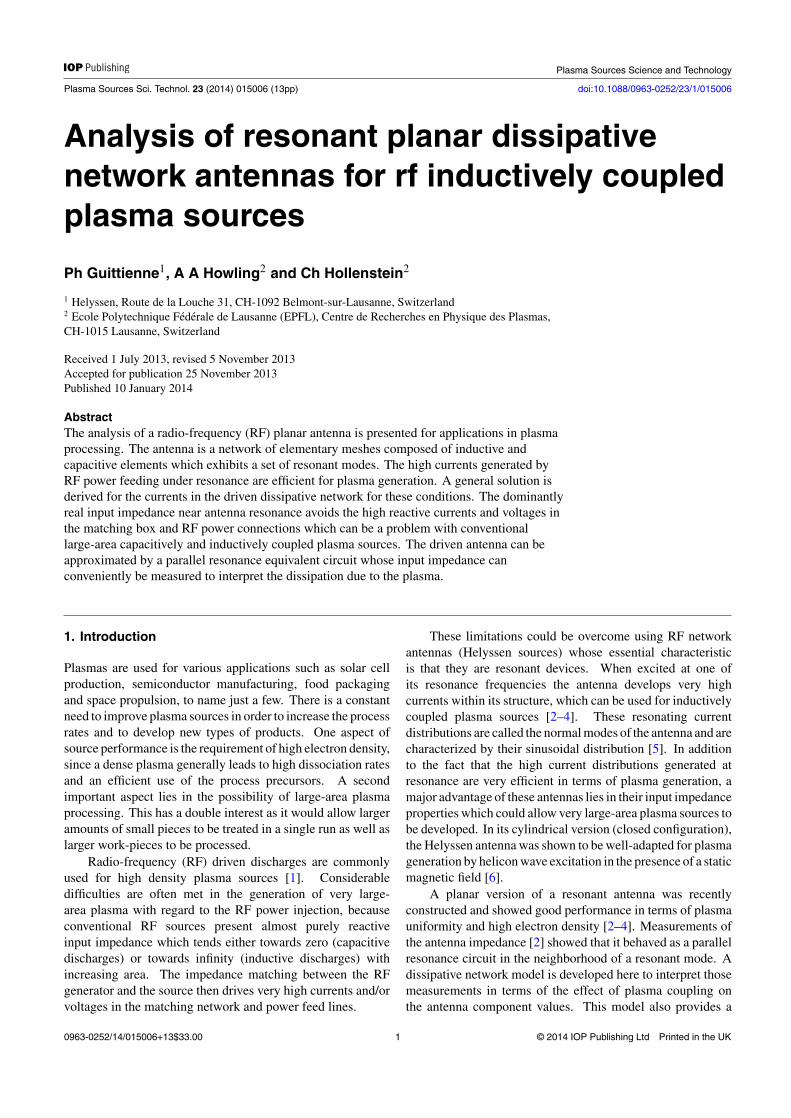
Figure 1. High-pass dissipative ladder network made up of identicalmeshes, showing the leg inductances L with resistances R, linked bycapacitances C with short connections of inductance M andresistance r .
basic theoretical framework to optimize the antenna designwith regard to current uniformity and input impedance, inorder to further develop the resonant network for plasma sourceapplications. Experimental measurements of the influence ofthe mode structure on plasma uniformity [7] will be discussedin future work.
The first part of this study describes the normal modes ofthe antenna, the second part gives a general solution for thecurrents of driven dissipative antennas, and in the third part,a parallel resonance equivalent circuit is derived in terms ofthe antenna components and their modifications due to plasmacoupling.
2. Resonant planar network as an inductivelycoupled plasma source
This work describes the principles of the Helyssen planarantenna [8]. Its structure and operating principles aresimilar to the closed cylindrical birdcage antenna previouslydescribed [5, 6], but it is unwrapped to form an open andplanar structure, as shown in figure 1. The planar structureis a segment of a ladder network which can also be called anopen coil (or antenna) in the literature [5]. The planar antennais suited for surface treatment of large flat areas, whereas thecylindrical version can be used as a volume plasma source forimmersion of work-pieces [7]. Even though their applicationsare different, the circuit analysis of open and closed antennas isonly distinguished by the boundary conditions inherent to theirstructure [5]. The closed antenna (birdcage) is well known fornuclear magnetic resonance (NMR) measurements where them = 1 mode is used to generate a uniform RF magnetic fieldto excite the nuclear spins in biological samples [5]. Drivenbirdcage resonators with losses were recently considered byNovikov [9] using low impedance voltage sources applied tosingle mesh elements. Pascone et al [10] and Tropp [11] treatedthe birdcage resonator as a lossy transmission line. Otherauthors [12, 13] represented the dissipation as an effective coilresistance. In this paper, we consider the general case of adissipative planar resonant antenna, with arbitrary positionsfor the RF connections along one side, applied as a plasmasource.
Throughout this work, a discrete component (lumpedelement) equivalent circuit analysis will be used. This isvalid provided that all circuit dimensions are small comparedwith the wavelength of the RF excitation. Electromagnetic
effects due to large dimensions and high frequencies will beconsidered in later work.
The balanced high-pass passive filter ladder networkshown in figure 1 has shunt inductors and series capacitors.The inductors consist of conducting legs (rungs), regularlydistributed, with each one connected at both ends to its closestneighbors by capacitors. In the RF range (1–100 MHz), thelegs can be approximated by self-inductances L having a smallresistance R. The high-quality-factor capacitors C in the twoside-branches (the stringers) have metal leads to link the rungstogether, having self-inductance M and resistance r . To a firstorder approximation for a dissipative antenna, therefore, thestringer impedances are Z1 = 1/(jωC) + jωM + r , and the legimpedances are Z2 = R + jωL, where ω is the RF angularfrequency. The mutual inductance between all conductingparts has a strong influence on the mode frequencies [5], but itscalculation is beyond the scope of this work. On the other hand,the mode structure of the currents and voltages calculated hereis not strongly perturbed by the mutual inductance effect [2].The general formulation given in this work can be applied toany configuration provided that the network is made up ofidentical elementary meshes. We consider high-pass networksas a specific example for plasma applications, although otherresonant antenna configurations can also be envisaged (low-pass, hybrid, etc).
Experiments on rf network antennas for large-area andlarge-volume inductively coupled plasma sources have beendescribed in [7] where it was shown that further understandingof the antenna–plasma coupling requires an analysis of thedissipative network antenna. As an example, the data pointsin figure 2(a) show the impedance of a planar 23-leg antennameasured without plasma [2]. The fitted line demonstratesthat the network of figure 1 can be well represented by aparallel resonance equivalent circuit. In the presence of a lowpressure gas, capacitive coupling from the high-voltage pointson the antenna ignites a plasma; the antenna input impedancedoes not change significantly because the capacitance betweenthe antenna and plasma is small compared with the antennacapacitances C [7]. As the antenna input power is raised,currents induced in the plasma then cause a transition to aninductively coupled plasma [7, 14–18]. The input impedanceof the antenna changes strongly as shown by the example infigure 2(b). This change is due to plasma–antenna couplingby transformer action as described by Piejak et al [14].
In this case, each leg in figure 1 can be considered tobe a primary circuit (self-inductance L0, resistance R0, infigure 3) which induces a skin current in the plasma. Thisinduced current can be considered as a secondary circuit havinga geometric (or magnetic) self-inductance L2 and a plasmaimpedance [14]. The plasma impedance is proportional to theplasma complex (vector) resistivity ρ = (ν + jω)me/(nee
2),where me and ne are the electron mass and number density andν is the effective electron collision frequency due to collisionswith the neutral gas [1]. Hence, if the resistance of the plasmacurrent path in the secondary circuit has a value R2, then thereactance of this plasma current path is jωR2/ν, with respect tothe ratio of the real and imaginary parts of the plasma resistivity.This plasma reactance can be written as an effective plasma
2

Plasma Sources Sci. Technol. 23 (2014) 015006 Ph Guittienne et al
Figure 2. The antenna impedance magnitude (squares) and phase(circles) measured in the neighborhood of the m = 6 mode (a)without plasma; and (b) with a low power plasma (80 W) in 5 Pa ofargon. The lines show fitted curves using a parallel resonanceequivalent circuit for each case: (a) 13.13 nF in parallel with a seriescombination of 10.55 nH and 2.65 m; (b) 15.09 nF in parallel witha series combination of 9.166 nH and 6.68 m. The dotted linesshow the shift in the resonance frequency from 13.525 MHz(without plasma) to 13.532 MHz for the low power plasma. Datataken from [2].
inductance Le = R2/ν, as shown schematically in figure 3,which is physically due to electron inertia [14].
The induced current can be approximated as an imagecurrent in a perfectly conducting plane at some arbitraryposition in the plasma, such as at half the skin depth from theantenna–plasma interface [19]. Values for L0, L2, and theirmutual inductance M02 can be calculated using expressionsfor the inductance of linear conductors and the image currentmethod [20]. The impedance of each leg in the presence ofplasma inductive coupling is given by the series equivalentcircuit in figure 3 where the secondary (plasma) circuit istransformed in terms of the primary circuit current [14, 21].Finally, the leg impedance Z2 = R + jωL in figure 1 isrepresented by R0 + jωL0 in the absence of plasma, and(R0 + aR2) + jω(L0 − aL2 − aR2/ν) in the presence ofplasma inductive coupling [14], where a = ω2M2
02/[(ωL2 +
leg,primarycircuit
L0
R0
ip
L2
R2
is
M02
plasma,secondary
circuit
leg seriesequivalent
circuit
L
R
ip
transform
Le
Figure 3. Electrical circuit of the current ip in the leg (primarycircuit: self-inductance L0, resistance R0) inductively coupled withthe plasma current is (secondary circuit: self-inductance L2, plasmaresistance R2, plasma self-inductance Le), via their mutualinductance M02. The secondary circuit can be transformed into aseries equivalent circuit (total self-inductance L, total resistance R)in terms of the primary circuit current. The notation of [14] is used.
R2ω/ν)2 + R22] is a transformation factor. Hence the analysis
of the antenna network properties can be carried out using thecircuit of figure 1, on the understanding that the value of Z2 =R + jωL depends on whether there is plasma or not. Note thatinductive coupling to the plasma increases the leg resistanceby aR2, and decreases the leg inductance by (aL2 + aR2/ν).The stringer impedances Z1 are also transformed by plasmacoupling although the effect is relatively small because thestringers are short compared with the legs.
It is interesting to note that the particular case of a linearconductor coupled with a conducting, dissipative medium canalso be analyzed by the complex-image method [22–24] whichgives a self-consistent calculation of the line impedance interms of the medium conductivity. There is then no need toassume a perfectly conducting plane at an arbitrary position.However, comparison between the transformer method aboveand the complex-image method goes beyond the scope ofthis work.
Estimation of the plasma parameters using the antennainput impedance measurements of figure 2 is consideredfurther in section 5.1. First of all, however, in the followingsections it is necessary to calculate the relation between theantenna input impedance and the impedances of the legs andstringers which make up the network [7].
3. Normal modes in ladder networks
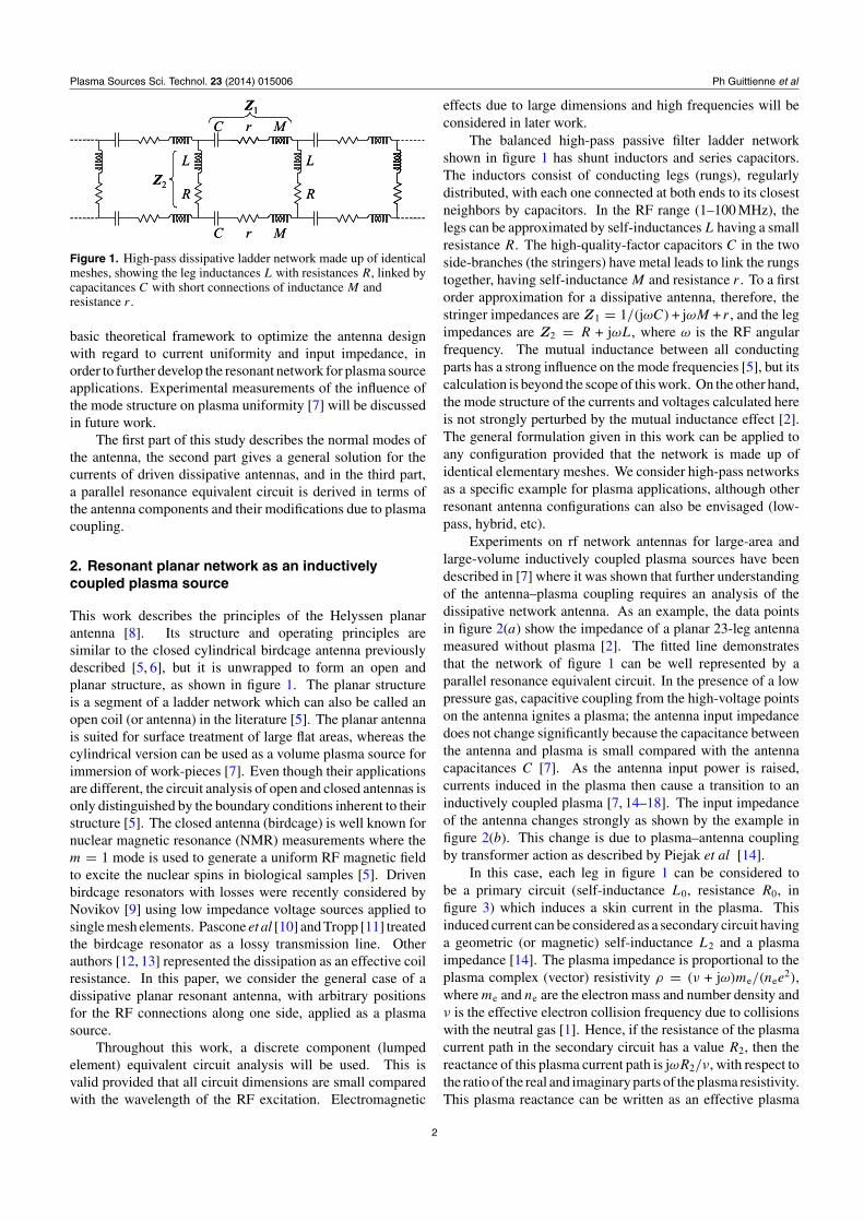
In figure 4, In, Mn and Kn are currents while An and Bn
denote the potentials at the antenna nodes. Ladder networksare conventionally analysed using a loop current description[5], where the loop current Jn in each section is given byJn = Mn = −Kn, and In = Jn −Jn−1. However, to treat thegeneral case of a dissipative-driven antenna in section 4, wewill have to introduce into the circuit analysis the input currentirf driven by the antenna RF power supply. This injection ofRF current means that Mn = −Kn does not hold everywhereon the antenna, and so the loop current description cannotbe used for the dissipative-driven antenna. For consistentnotation throughout this work, we will therefore use Kn and
3
Plasma Sources Sci. Technol. 23 (2014) 015006 Ph Guittienne et al
Figure 4. A ladder network segment with N legs made up of stringer impedances Z1 and leg impedances Z2.
Mn instead of loop currents Jn. A derivation of the normalmode frequencies and current distributions [5] is now brieflyreviewed to introduce the notation and to give a reference pointfor comparison of the general solution for dissipative antennasin section 4.
3.1. General solution for the leg currents, In
For the currents and impedances defined in the nth elementarymesh of figure 4, the general set of equations for the circuitanalysis is given by Kirchhoff’s and Ohm’s laws for thecurrents and voltages,
Mn = Mn−1 + In, (1)
Kn = Kn−1 − In, (2)
Z2In + Z1Mn − Z2In+1 − Z1Kn = 0. (3)
A recurrence relation for the leg currents In is obtained bysubtracting the voltage equation for the (n − 1)th mesh andeliminating Mn and Kn using (1) and (2):
In+1 − 2
(1 +
Z1
Z2
)In + In−1 = 0. (4)
The conventional solution is In = a1Γn1 + a2Γn
2, where Γ1 andΓ2 are the roots of the quadratic characteristic equation whichcan be arranged as
Γ + 1/Γ2
=(
1 +Z1
Z2
). (5)
Recognizing that these roots are reciprocal, we write Γ1 = e−γ
and Γ2 = eγ , whereupon the characteristic equation becomes
cosh γ =(
1 +Z1
Z2
), (6)
and the general solution for the antenna leg currents is therefore
In = a1e−γn + a2eγn, (7)
where a1 and a2 are complex constants to be determinedfrom boundary conditions. The solution given by (6) and(7) holds for any impedances Z1 and Z2, and is thereforevalid for dissipative antennas also. For harmonic currents
with ejωt time dependence, the leg currents are Inejωt sothat the general solution is seen to consist of a forwardtraveling wave a1 exp(jωt − γn) and a backward travelingwave a2 exp(jωt + γn), where γ = α + jβ is the propagationconstant, α is the attenuation constant per section and β is thephase change per section (α and β are both real).
3.2. Normal modes for a non-dissipative planar antenna
For a non-dissipative ladder network, the impedances Z1 =1/(jωC) + jωM and Z2 = jωL are purely imaginary andtheir ratio in (6) is purely real. The propagation constant thencorresponds to γ = jβ in (6):
cos β = 1 +M
L− 1
ω2LC. (8)
For this special case of a lossless antenna, there is noinjection of RF current to consider and so Mn = −Kn. Using(1)–(3) gives the same recurrence relation as for In, henceMn = −Kn = b1e−jβn + b2ejβn. Recognizing that M0 = 0from figure 4, we have b1 = −b2, and the currents Mn in thenon-dissipative ladder network are therefore proportional tosin(nβ). The finite length condition MN = 0 further impliesthat Nβ = mπ . When combined with (8), this leads to theexistence of normal mode frequencies [5]
ωm = 1√C
(M + 2L sin2
(mπ
2N
)) ,
(m = 1, 2, . . . , N − 1), (9)
and imposes the spatial distribution for Mn:
Mn ∝ sin(nmπ
N
), (m = 1, 2, . . . , N − 1), (10)
where the phase shift per section β = mπN
is proportional to themode number m. The normal mode current in each leg, using(10) in (1), is given by [5]
In ∝ sin(mπ
2N
)cos
[(n − 1
2
)mπ
N
],
(m = 1, 2, . . . , N − 1). (11)
To summarize, a N -leg lossless planar antenna presents(N − 1) normal modes [5] whose current amplitudes havesinusoidal spatial distributions and which oscillate in phase.
4
Plasma Sources Sci. Technol. 23 (2014) 015006 Ph Guittienne et al
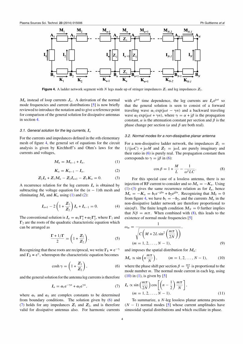
Figure 5. Equivalent circuit of a Helyssen-driven planar antenna showing the three parts I, II, and III. The driving current irf from the RFpower supply is fed into the antenna via node n = Nf with the return path via node Ng. The boundaries between the three parts are definedby the nodes Ng and Nf , where Ng < Nf in this work.
4. Dissipative networks: Helyssen plasma sources
A real antenna dissipates power due to the electrical resistanceof its components. Furthermore, when used as a plasmasource, power injected into the antenna is partially transferredto the plasma by coupling to the dissipative medium. Thequestion then arises as to whether the resonance propertiesof non-dissipative antennas are preserved in the presenceof such a coupling to efficiently maintain a well-controlledplasma source. In the following, the resistances R and r areresponsible for the power dissipation, and the impedances arenow Z1 = r + 1/(jωC) + jωM and Z2 = R + jωL. Foran antenna used as an inductively coupled plasma source, arealistic value for R would not be more than a few ohms (anestimate of R < 122 m is derived in section 5.1).
We define a Helyssen planar resonant antenna as a driven,dissipative ladder network with arbitrary feed-point positionsfor the RF power connections, as shown in figure 5. This workconsiders the following points for antenna design:
(i) The values of the antenna input impedance and the antennacomponents L, R, C, M, r;
(ii) Optimum design of the connection configuration and thechoice of mode;
(iii) Estimation of the current and mode perturbations due tothe injected rf driving current, and the effect of plasma onthe antenna impedance and its component values.
4.1. Current distribution in a dissipative antenna with arbitraryconnection configuration
Because of current injection irf from the RF power supply(figure 5), a single solution for the whole antenna can no longerbe found. Instead, separate solutions have to be determinedfor each part of the antenna, with respect to the boundaryconditions at the nodes of current injection.
The total net current along the line is iline = Mn +Kn. Byadding (1) and (2), iline = Mn + Kn = Mn−1 + Kn−1 whichis constant along a line segment if not interrupted by current
injection nodes. For current continuity, referring to figure 5,iline = 0 in parts I and III, and iline = −irf in part II of theline which carries the RF current circulating via the RF powersupply.
For antenna impedance calculations, it will also benecessary to consider the RF voltages An and Bn at the antennanodes in figure 5. The voltages across the antenna impedances,by Ohm’s law, are
An − An+1 = Z1Mn, (12)
Bn − Bn+1 = Z1Kn, (13)
Bn − An = Z2In. (14)
The sum of (12) and (13) is (An + Bn) − (An+1 + Bn+1) =Z1(Mn + Kn) from which the sum of voltages at the nth nodecan be written as
An + Bn = V0 − nZ1iline, (15)
where V0 is a different constant for each part. Using (14) and(15), the node voltages in terms of the dissipative antenna legcurrents In are
An = [V0 − nZ1iline − Z2In] /2, (16)
Bn = [V0 − nZ1iline + Z2In] /2, (17)
where iline = 0 for parts I and III, and iline = −irf in part II asabove. The stringer currents are then found using (12) and (13):
Mn =[iline +
Z2
Z1(In+1 − In)
]/2, (18)
Kn =[iline − Z2
Z1(In+1 − In)
]/2, (19)
where it can be seen that, in part II of the antenna, thecirculating RF current iline = −irf is shared equally betweenthe two stringers of the antenna.
The solution for the currents in the dissipative antenna isshown in appendix A, and figure 6 shows the calculated current
5

Plasma Sources Sci. Technol. 23 (2014) 015006 Ph Guittienne et al
Figure 6. Driven RF currents in a dissipative antenna calculated for RF connection points Nf = 12 and (a) Ng = 8, or (b) Ng = 4. Left: legcurrents In, where the RF connection positions are marked by circles. Right: stringer currents, full line Mn, dashed line Kn. Representativeexperimental antenna component values: N = 23 legs, L = 143 nH, R = 36 m, C = 2.6 nF, M = 7.9 nH, r = 2 m. Mode m = 6, attime exp(jωt) = exp(jπ/4) for RF current |irf | = 1 A.
distribution in the legs and stringers of a dissipative antennacorresponding to an experimental arrangement [2, 3]. Twocases are shown: (a) for feed-points (Ng, Nf) = (8, 12) wherethe antenna resonant currents are much larger than irf ; and (b)
for feed-points (Ng, Nf) = (4, 12) where irf is comparable tothe antenna currents. The arrows in (b) mark the differencesin the Mn currents at nodes Ng and Nf which arise to respectcurrent continuity with the RF current injection. From the pointof view of current uniformity, it is clearly necessary to arrangefor the RF input current to be as small as possible comparedwith the antenna currents.
At resonance, in the limit of weak dissipation, α → 0, thecurrent distributions (A.1)–(A.3) in all three parts tend towardsthe same limit (see section B.1 in the appendix):(
In
irf
)α→0
(
j
αN
)· sin
(mπ
2N
)cos
[(n − 1
2
)mπ
N
]
·
D
cos(mπ
2N
) , (20)
D = cos
[(Ng − 1
2
)mπ
N
]− cos
[(Nf − 1
2
)mπ
N
]. (21)
The first bracket of (20) shows that the RF driving current irf isin phase quadrature (j = eiπ/2) with respect to the leg currentsIn. The inverse dependence on α means that the drivingcurrent becomes negligible compared with the leg currents,|irf | |In|, in the limit of a lossless antenna, i.e. a non-zero
resonant current persists as the driving current tends to zero.The (sin, cos) product in (20) shows that the normal modecurrent distribution (11) is recovered for a weakly dissipativeantenna. Also, the amplitude of the spatial distribution of legcurrents becomes uniform along all three parts of the antennain the normal mode limit α → 0 because the driving currentirf becomes negligible compared with In. The factor D in (20)accounts for the choices of mode number m and of RF currentinjection connections (Ng, Nf). When the injection pointscoincide with a maximum and a minimum in the leg currents,as for (Ng, Nf) = (8, 12) in figure 6(a), the RF excitation isefficiently coupled to the antenna resonant current distribution,then |In/irf | 1, and |D| = 1.99 is close to its maximumof 2. Conversely, when the RF connections positions do notcorrespond to the normal mode spatial variation of the legcurrents, as for (Ng, Nf) = (4, 12) in figure 6(b), the drivencurrents In are not large compared with the RF current, and|D| = 0.037 is close to zero. The importance of D for theantenna input impedance is described in section 4.3.
4.2. Input impedance of a dissipative antenna
The input impedance of a Helyssen antenna determines therequired level of driven RF current for a given power injection,and determines the parameters necessary for matching theantenna to the power source output impedance. In figure 5, theRF voltage, Vrf , across the input nodes is given by ANf −ANg .
6
Plasma Sources Sci. Technol. 23 (2014) 015006 Ph Guittienne et al
5 10 15 20
10−2
100
102
mode number m = 1 − 22
ℜ(Z
in) [Ω
]
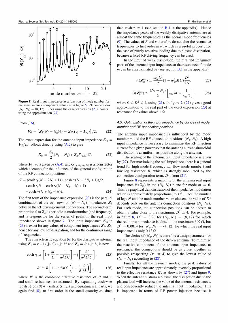
Figure 7. Real input impedance as a function of mode number forthe same antenna component values as in figure 6. RF connections(Ng, Nf) = (8, 12). Lines using the exact expression (23); pointsusing the approximation (27).
From (16),
Vrf = [Z1(Nf − Ng)irf − Z2(INf − INg)
]/2. (22)
The exact expression for the antenna input impedance Zin =Vrf/irf follows directly using (A.2) to give
Zin = Z1
2(Nf − Ng) + Z2F(γ,N)G, (23)
where F(γ,N) is given by (A.4), and G(γ,Ng,Nf ,N) is a form factorwhich accounts for the influence of the general configurationof the RF connection positions:
G = (cosh γ(N − 2Nf + 1) + cosh γ(N − 2Ng + 1))/2
+ cosh γN − cosh γ(N − Ng − Nf + 1)
− cosh γ(N + Ng − Nf). (24)
The first term of the impedance expression (23) is the parallelcombination of the two rows of (Nf − Ng) impedances Z1
between the RF driving current connections. The second term,proportional to Z2, is periodic in mode number (and frequency)and is responsible for the series of peaks in the real inputimpedance shown in figure 7. The input impedance Zin in(23) is exact for any values of component impedances Z1, Z2,hence for any level of dissipation, and for the continuous rangeof frequencies.
The characteristic equation (6) for the dissipative antenna,using Z1 = r + 1/(jωC) + jωM and Z2 = R + jωL, is now
cosh γ [
1 +M
L− 1
ω2LC
]− j
[R′
ω3L2C
], (25)
R′ R
[1 − ω2MC
(1 − r
R
L
M
)], (26)
where R′ is the combined effective resistance of R and r ,and small resistances are assumed. By expanding cosh γ =(cosh α)(cos β) + j(sinh α)(sin β) and equating real parts, weagain find (8), to first order in the small quantity α, since
then cosh α 1 (see section B.1 in the appendix). Hencethe impedance peaks of the weakly dissipative antenna are atalmost the same frequencies as the normal mode frequencies(9). The values of R and r therefore do not alter the resonancefrequencies to first order in α, which is a useful property forthe case of purely resistive loading due to plasma dissipation,because a fixed RF driving frequency can be used.
In the limit of weak dissipation, the real and imaginaryparts of the antenna input impedance at the resonance of modem can be approximated by (see section B.1 in the appendix):
(Zresin ) ω2
mL2
R′ (1 − w2mMC)
D2
2N, (27)
(Zresin ) (Nf − Ng)
2
[ωmM − 1
ωmC
], (28)
where 0 D2 4, using (21). In figure 7, (27) gives a goodapproximation to the real part of the exact expression (23) atresonance for values above 1 .
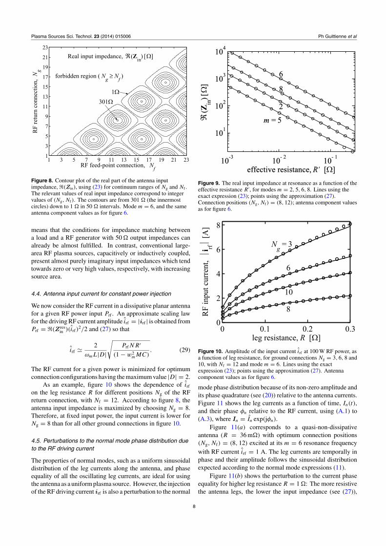
4.3. Optimization of the input impedance by choices of modenumber and RF connection positions
The antenna input impedance is influenced by the modenumber m and the RF connection positions (Ng, Nf). A highinput impedance is necessary to minimize the RF injectioncurrent for a given power so that the antenna current sinusoidaldistribution is as uniform as possible along the antenna.
The scaling of the antenna real input impedance is givenby (27). For maximizing the real impedance, there is a generaltrend for high mode frequency ωm (low mode number) andlow leg resistance R, which is strongly modulated by theconnection configuration term, D2, from (21).
Figure 8 represents a mapping of the antenna real inputimpedance (Zin) in the (Ng, Nf) plane for mode m = 6.This is a graphical demonstration of the impedance modulationwhich is approximately proportional to D2. Once the numberof legs N and the mode number m are chosen, the value of D2
depends only on the antenna connection positions (Ng, Nf).For each mode, the connection positions can be chosen toobtain a value close to the maximum, D2 4. For example,in figure 8, D2 = 3.96 for (Ng, Nf) = (8, 12) for whichthe real input impedance is close to the maximum 302 , butD2 = 0.0014 for (Ng, Nf) = (4, 12) for which the real inputimpedance is only 0.13 .
The choice of (Ng, Nf) is therefore a design parameter forthe real input impedance of the driven antenna. To minimizethe reactive component of the antenna input impedance atresonance, the connections should be as close together aspossible (respecting D2 ≈ 4) to give the lowest value of(Nf − Ng) according to (28).
Finally, for all the resonant modes, the peak values ofreal input impedance are approximately inversely proportionalto the effective resistance R′, as shown by (27) and figure 9.When the antenna sustains a plasma, the dissipation due to theplasma load will increase the value of the antenna resistances,and consequently reduce the antenna input impedance. Thisis important in terms of RF power injection because it
7
Plasma Sources Sci. Technol. 23 (2014) 015006 Ph Guittienne et al
1 3 5 7 9 11 13 15 17 19 21 231
3
5
7
9
11
13
15
17
19
21
23
RF feed−point connection, Nf
RF
ret
urn
conn
ecti
on,
Ng
forbidden region ( Ng
≥ Nf)
Real input impedance, ℜ(Zin
) [Ω]
1Ω
301Ω
Figure 8. Contour plot of the real part of the antenna inputimpedance, (Zin), using (23) for continuum ranges of Ng and Nf .The relevant values of real input impedance correspond to integervalues of (Ng, Nf). The contours are from 301 (the innermostcircles) down to 1 in 50 intervals. Mode m = 6, and the sameantenna component values as for figure 6.
means that the conditions for impedance matching betweena load and a RF generator with 50 output impedances canalready be almost fulfilled. In contrast, conventional large-area RF plasma sources, capacitively or inductively coupled,present almost purely imaginary input impedances which tendtowards zero or very high values, respectively, with increasingsource area.
4.4. Antenna input current for constant power injection
We now consider the RF current in a dissipative planar antennafor a given RF power input Prf . An approximate scaling lawfor the driving RF current amplitude irf = |irf | is obtained fromPrf = (Zres
in )(irf)2/2 and (27) so that
irf 2
ωmL|D|
√PrfNR′
(1 − w2mMC)
. (29)
The RF current for a given power is minimized for optimumconnection configurations having the maximum value |D| = 2.
As an example, figure 10 shows the dependence of irf
on the leg resistance R for different positions Ng of the RFreturn connection, with Nf = 12. According to figure 8, theantenna input impedance is maximized by choosing Ng = 8.Therefore, at fixed input power, the input current is lower forNg = 8 than for all other ground connections in figure 10.
4.5. Perturbations to the normal mode phase distribution dueto the RF driving current
The properties of normal modes, such as a uniform sinusoidaldistribution of the leg currents along the antenna, and phaseequality of all the oscillating leg currents, are ideal for usingthe antenna as a uniform plasma source. However, the injectionof the RF driving current irf is also a perturbation to the normal
10−3
10− 2
10− 1
101
102
103
104
effective resistance, R' [Ω]
ℜ(Z
in) [Ω
]
2
m = 5
6
8
Figure 9. The real input impedance at resonance as a function of theeffective resistance R′, for modes m = 2, 5, 6, 8. Lines using theexact expression (23); points using the approximation (27).Connection positions (Ng, Nf) = (8, 12); antenna component valuesas for figure 6.
0 0.1 0.2 0.30
2
4
6
8
leg resistance, R [Ω]
RF
inpu
t cur
rent
, i
rf
[A]
Ng = 3
6
8
10
Figure 10. Amplitude of the input current irf at 100 W RF power, asa function of leg resistance, for ground connections Ng = 3, 6, 8 and10, with Nf = 12 and mode m = 6. Lines using the exactexpression (23); points using the approximation (27). Antennacomponent values as for figure 6.
mode phase distribution because of its non-zero amplitude andits phase quadrature (see (20)) relative to the antenna currents.Figure 11 shows the leg currents as a function of time, In(t),and their phase φn relative to the RF current, using (A.1) to(A.3), where In = In exp(jφn).
Figure 11(a) corresponds to a quasi-non-dissipativeantenna (R = 36 m) with optimum connection positions(Ng, Nf) = (8, 12) excited at its m = 6 resonance frequencywith RF current irf = 1 A. The leg currents are temporally inphase and their amplitude follows the sinusoidal distributionexpected according to the normal mode expressions (11).
Figure 11(b) shows the perturbation to the current phaseequality for higher leg resistance R = 1 : The more resistivethe antenna legs, the lower the input impedance (see (27)),
8

Plasma Sources Sci. Technol. 23 (2014) 015006 Ph Guittienne et al
Figure 11. Left: currents in all the antenna legs, and the RF current, as a function of time for one RF period at 13.56 MHz. Right: theirphases referenced to the RF feed-point driving current at 90, for irf = 1 A. (a) Optimum connections (Ng, Nf) = (8, 12) and low legresistance R = 36 m; (b) optimum connections but high leg resistance, R = 1 ; (c) low leg resistance (R = 36 m) but non-optimumconnections (Ng, Nf) = (4, 12). The phases for the RF driving current are labelled by irf . Mode m = 6, with antenna component values asfor figure 6 unless otherwise stated.
and the lower the leg currents with respect to the RF current.The equivalent circuit approach in section 5 will be used toestimate the increase in the effective leg resistance due toplasma loading.
Figure 11(c) shows the effect of the connectionconfiguration D on the phase equality of the antenna currentsby changing the ground connection position to Ng = 4. Thecurrent phase equality is strongly perturbed even though theleg resistance has the same low value as for figure 11(a).The perturbed distribution is due to the low input impedanceassociated with the Ng = 4 feeding configuration.
Since dissipative coupling to the plasma increases thevalue of R, it is all the more important that the connectionconfiguration be chosen so that D2 4 to obtain the maximum
value of the real input impedance. In terms of plasmageneration, situations (b) and (c) would cause non-uniformitiesin heating and electron density. To maintain the amplitudeuniformity and phase equality of normal modes, it is thereforenecessary that the leg current amplitude be as large as possiblecompared with the RF current, which is obtained for high inputimpedance.
5. Parallel resonance approximation for the inputimpedance near to a resonance frequency
In the neighborhood of a resonance frequency, each peak infigure 7 has a form similar to the parallel resonance behaviormeasured experimentally [2] with and without plasma, as
9
Plasma Sources Sci. Technol. 23 (2014) 015006 Ph Guittienne et al
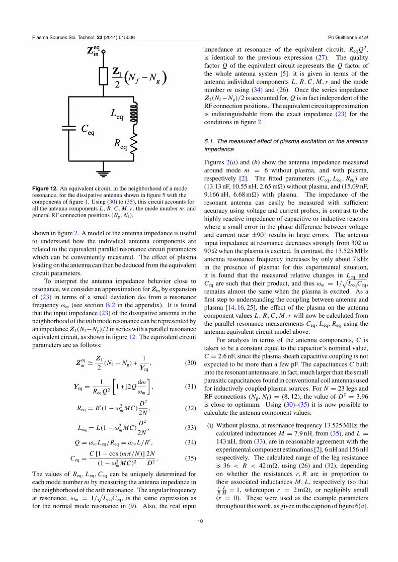
Figure 12. An equivalent circuit, in the neighborhood of a moderesonance, for the dissipative antenna shown in figure 5 with thecomponents of figure 1. Using (30) to (35), this circuit accounts forall the antenna components L, R, C, M, r , the mode number m, andgeneral RF connection positions (Ng, Nf).
shown in figure 2. A model of the antenna impedance is usefulto understand how the individual antenna components arerelated to the equivalent parallel resonance circuit parameterswhich can be conveniently measured. The effect of plasmaloading on the antenna can then be deduced from the equivalentcircuit parameters.
To interpret the antenna impedance behavior close toresonance, we consider an approximation for Zin by expansionof (23) in terms of a small deviation dω from a resonancefrequency ωm (see section B.2 in the appendix). It is foundthat the input impedance (23) of the dissipative antenna in theneighborhood of themth mode resonance can be represented byan impedance Z1(Nf−Ng)/2 in series with a parallel resonanceequivalent circuit, as shown in figure 12. The equivalent circuitparameters are as follows:
Zeqin Z1
2(Nf − Ng) +
1
Yeq, (30)
Yeq = 1
ReqQ2
[1 + j2Q
dω
ωm
], (31)
Req = R′(1 − ω2mMC)
D2
2N, (32)
Leq = L(1 − ω2mMC)
D2
2N, (33)
Q = ωmLeq/Req = ωmL/R′, (34)
Ceq = C [1 − cos (mπ/N)]
(1 − ω2mMC)2
2N
D2. (35)
The values of Req, Leq, Ceq can be uniquely determined foreach mode number m by measuring the antenna impedance inthe neighborhood of the mth resonance. The angular frequencyat resonance, ωm = 1/
√LeqCeq, is the same expression as
for the normal mode resonance in (9). Also, the real input
impedance at resonance of the equivalent circuit, ReqQ2,
is identical to the previous expression (27). The qualityfactor Q of the equivalent circuit represents the Q factor ofthe whole antenna system [5]: it is given in terms of theantenna individual components L, R, C, M, r and the modenumber m using (34) and (26). Once the series impedanceZ1(Nf −Ng)/2 is accounted for, Q is in fact independent of theRF connection positions. The equivalent circuit approximationis indistinguishable from the exact impedance (23) for theconditions in figure 2.
5.1. The measured effect of plasma excitation on the antennaimpedance
Figures 2(a) and (b) show the antenna impedance measuredaround mode m = 6 without plasma, and with plasma,respectively [2]. The fitted parameters (Ceq, Leq, Req) are(13.13 nF, 10.55 nH, 2.65 m) without plasma, and (15.09 nF,9.166 nH, 6.68 m) with plasma. The impedance of theresonant antenna can easily be measured with sufficientaccuracy using voltage and current probes, in contrast to thehighly reactive impedance of capacitive or inductive reactorswhere a small error in the phase difference between voltageand current near ±90 results in large errors. The antennainput impedance at resonance decreases strongly from 302 to90 when the plasma is excited. In contrast, the 13.525 MHzantenna resonance frequency increases by only about 7 kHzin the presence of plasma: for this experimental situation,it is found that the measured relative changes in Leq andCeq are such that their product, and thus ωm = 1/
√LeqCeq,
remains almost the same when the plasma is excited. As afirst step to understanding the coupling between antenna andplasma [14, 16, 25], the effect of the plasma on the antennacomponent values L, R, C, M, r will now be calculated fromthe parallel resonance measurements Ceq, Leq, Req using theantenna equivalent circuit model above.
For analysis in terms of the antenna components, C istaken to be a constant equal to the capacitor’s nominal value,C = 2.6 nF, since the plasma sheath capacitive coupling is notexpected to be more than a few pF. The capacitances C builtinto the resonant antenna are, in fact, much larger than the smallparasitic capacitances found in conventional coil antennas usedfor inductively coupled plasma sources. For N = 23 legs andRF connections (Ng, Nf) = (8, 12), the value of D2 = 3.96is close to optimum. Using (30)–(35) it is now possible tocalculate the antenna component values:
(i) Without plasma, at resonance frequency 13.525 MHz, thecalculated inductances M = 7.9 nH, from (35), and L =143 nH, from (33), are in reasonable agreement with theexperimental component estimations [2], 6 nH and 156 nHrespectively. The calculated range of the leg resistanceis 36 < R < 42 m, using (26) and (32), dependingon whether the resistances r, R are in proportion totheir associated inductances M, L, respectively (so thatrR
LM
= 1, whereupon r = 2 m), or negligibly small(r = 0). These were used as the example parametersthroughout this work, as given in the caption of figure 6(a).
10

Plasma Sources Sci. Technol. 23 (2014) 015006 Ph Guittienne et al
(ii) With plasma, at resonance frequency 13.532 MHz, thecalculated inductances are now M = 10.7 nH and L =134 nH. The calculated range of the leg resistance is97 < R < 122 m, again depending on how r isestimated. The strong increase in resistance R due toplasma loading (see figure 3 and accompanying text) isnot so large as to perturb the phase equality of the legcurrents. The leg inductance L has diminished by 9 nH,whereas the small inductance M is estimated to increaseby almost 3 nH. The error is estimated to be not more than1 nH for both inductances. On the basis of this model, theincrease in M in (35) accounts for the measured increasein Ceq which is responsible for the almost-unchangedresonance frequency when the plasma is excited. Thedecrease in L could be interpreted as the consequence ofinductive coupling between the antenna and the plasma[14, 16, 25] as discussed in section 2. However, theapparent increase in M cannot be understood on this basissince plasma inductive coupling would be expected todecrease the inductance of all conducting elements. Infact, the observed frequency shift is not only determinedby inductive coupling to the plasma but also by thepartial screening by the plasma of the mutual inductancesbetween the legs [7]. The estimations of changes inresistance and inductance remain valid, but an analysisof plasma parameters based on section 2 and antennainput impedance measurements would require knowledgeof the inductance change due to transformer coupling,separately from the mutual impedance effect. However,the consideration of mutual inductances is beyond thescope of this paper. The real input impedances withand without plasma, calculated at resonance using (27)or ReqQ
2, are consistent with the measured values.
To summarize, the dominant effect of plasma excitation on theantenna is to triple the effective resistance of its legs. This isdue to antenna coupling with the dissipative plasma. For thisexample, the measured resonance frequency remains almostthe same when the plasma is excited, due to changes in theantenna inductances on the basis of this model. For use asan industrial plasma source [4], this is convenient becausea fixed frequency RF power generator can be used, and thedominantly real input impedance near to antenna resonanceavoids strong reactive currents and voltages in the RF powerfeeding which presents problems for conventional large-areaplasma sources. However, it remains difficult to understandthe details of antenna inductive coupling to the plasma withthis first modeling approach: for this, other mode frequencieswill have to be investigated, including an analysis of the mutualinductances between the antenna elements [5].
6. Conclusions
A theoretical analysis of Helyssen resonant antennas ispresented to aid antenna design for its development as a plasmasource for industrial applications. Analytical expressionsare given for the leg currents and the input impedance forarbitrary antenna impedances, and for any level of dissipation.Approximations are given for the case of a weakly dissipative
high-pass antenna to provide simple scaling laws. The antennacan be represented by a simple equivalent circuit whichincludes a parallel resonance circuit as shown by experimentswith and without plasma. Measurements of the equivalentcircuit during plasma excitation were interpreted in termsof the antenna component values. Inductive coupling tothe dissipative plasma tripled the leg effective resistance,whereas the resonant frequency was almost unchanged inthis case: the change in resonant frequency depends on bothplasma inductive coupling and on plasma screening of mutualinductances, which is more difficult to interpret than theincrease in effective resistance due to power dissipation in theplasma.
To design a planar antenna for an inductively coupledplasma source, it was shown that a high input impedance isnecessary to maintain the current amplitude uniformity andphase equality which are the desirable properties of normalmodes. This can be achieved by optimal choice of RFconnection positions for a given mode number in a weaklydissipative antenna. The dominantly real input impedance nearto antenna resonance avoids the problem of strong reactivecurrents and voltages in the matching box and RF powerconnections found in conventional large-area plasma sources.Further improvements to the model will require considerationof mutual inductances.
Acknowledgments
The authors thank M Chesaux for many useful comments. Thiswork was supported by Swiss Commission for Technology andInnovation grant no 9896.2 PFIW-IW.
Appendix A. The currents in the three parts of theantenna
The solution for the currents in the dissipative antenna isobtained by finding the constants a1 and a2 for the currentsIn in (7) for each part of the antenna. These six constantsare found using the boundary conditions at both ends (as insection 3.2) and with respect to current continuity betweenthe different parts at nodes n = Ng and n = Nf . Aftersome algebra, the leg currents for the general configuration offigure 5 are
I In = irfF(γ,N) [cosh g1 + cosh g2a − cosh g3 − cosh g4a] ,
(A.1)
I IIn = irfF(γ,N) [cosh g1 + cosh g2b − cosh g3 − cosh g4a] ,
(A.2)
I IIIn = irfF(γ,N) [cosh g1 + cosh g2b − cosh g3 − cosh g4b] ,
(A.3)
F(γ,N) = tanh(γ/2)
2 sinh(γN), (A.4)
where the arguments of the cosh functions
(i) g1 = γ(n − 1 + Ng − N),(ii) g2a = γ(n − Ng + N),
(iii) g2b = γ(n − Ng − N),
11

Plasma Sources Sci. Technol. 23 (2014) 015006 Ph Guittienne et al
(iv) g3 = γ(n − 1 + Nf − N),(v) g4a = γ(n − Nf + N),
(vi) g4b = γ(n − Nf − N),
represent the influence of the chosen RF connection positions(Ng, Nf). From (A.1)–(A.3) it can be seen that the currentflow in each element of a dissipative antenna is proportional tothe driving current irf , varies non-linearly with γ (via F ), anddepends on the RF connection positions. The importance ofthese three factors for the antenna input impedance, the antennacurrents, and their phases is discussed in sections 4.2–4.4.
Appendix B. Approximations by expansion in thesmall term α
B.1. Approximations at resonance
The factor F(γ,N), defined in (A.4), is used for the leg cur-rents (A.1)–(A.3) and the input impedance (23). For thelimit of small attenuation per section, α 1, the numera-tor tanh(γ /2) tanh(jβ/2) = j tan(β/2). In the denom-inator, sinh(γN) can be expanded as sinh(αN) cos(βN) +j cosh(αN) sin(βN) and since sin(βN) = sin(mπ) = 0 fornormal modes, we have sinh(γN) αN(−1)m for αN 1.One expression for F(γ,N) at resonance is therefore
F res(γ,N)
j tan
(mπ
2N
)2(−1)mαN
. (B.1)
Expansion of the sums of four cosh terms in (A.1)–(A.3) in thelimit of small α gives 2(−1)m cos[(n − 1
2 )mπN
]D for all threeof the sums. Taking the product with (B.1) gives the normalmode approximation for the current distribution in (20).
F res(γ,N) can also be expressed in terms of L, R, C, M, r by
expanding the characteristic equation as in (25). Equating realparts gives cos β [1+ M
L− 1
ω2mLC
] at resonance, and equatingimaginary parts gives
α sin β − R′
ω3L2C, (B.2)
for α 1 so that cosh α ≈ 1. For the example parametersin the caption of figure 6(a), α = 0.0015 and cosh α = 1, to6 decimal places. Using tan β
2 ≡ (1 − cos β)/ sin β in (B.1)gives the alternative expression
F res(γ,N) −jωmL(1 − w2
mMC)
2(−1)mNR′ , (B.3)
at resonance. In the expression for the input impedance (23),expansion of the cosh terms in G for small α gives (−1)mD2.In the limit of weak dissipation, Z2 jωL and hence the inputimpedance (23) at resonance can be approximated by (27) forthe real part and (28) for the imaginary part.
B.2. Approximations near to resonance
Normal modes excited in a lossless antenna present a discretefrequency spectrum whereas driven currents in a dissipativeantenna exhibit a continuous spectrum, with peaks of real
impedance at the normal mode resonance frequencies to firstorder in α (see (25)). For a dissipative antenna, therefore,the mode frequency has continuous values and we considera small variation in angular frequency dω about ωm, so thatω = ωm + dω. This corresponds to a mode variation dm
about mode number m (where dm 1). Whereas sin(βN) =sin(mπ) = 0 for normal modes, we now have sin(βN) =sin[(m + dm)π ] = cos(mπ) sin(π dm) (−1)mπ dm in theproximity of mode m. Expansion of sinh(γN) now gives
sinh(γN) (αN + jπ dm)(−1)m (B.4)
in the immediate neighborhood of the mth resonance, forαN 1. We now consider
1
Feq(γ,N)
= 2 sinh(γN)
tanh(γ/2)
2(−1)m[(α sin β)N + j(sin β)π dm]
j(1 − cos β), (B.5)
where sin β = −(2N/πω3mLC)(dω/dm) is obtained by
differentiating cos β [1 + (M/L) − (1/ω2mLC)] with
respect to m. Substituting into (B.5) and using (B.2)gives an approximation for the input impedance (23) in theneighborhood of the mth mode resonance:
Zeqin Z1
2(Nf − Ng) +
(1 − w2mMC)D2
2NYpar, (B.6)
where Ypar is the admittance of a parallel resonance circuithaving C in parallel with the series combination of L and R′:
Ypar 1
R′Q2
[1 + j2Q
dω
ωm
], (B.7)
and Q = ωmL/R′ is the quality factor of the antenna at theresonance frequency of the mth mode. Expressions (30)–(35)follow directly.
References
[1] Lieberman M A and Lichtenberg A J 2005 Principles ofPlasma Discharges and Materials Processing 2nd edn(Hoboken, NJ: Wiley)
[2] Guittienne Ph, Lecoultre S, Fayet P, Larrieu J, Howling A Aand Hollenstein Ch 2012 J. Appl. Phys. 111 083305
[3] Lecoultre S, Guittienne Ph, Howling A A, Fayet P andHollenstein Ch 2012 J. Phys. D: Appl. Phys. 45 082001
[4] Guittienne Ph, Fayet P, Larrieu J, Howling A A andHollenstein Ch 2012 55th Annual SVC (Surface VacuumCoaters) Technical Conf. (Santa Clara, CA, 28 April–3May)
[5] Jin J 1998 Electromagnetic Analysis and Design in MagneticResonance Imaging (Boca Raton, FL: CRC Press)
[6] Guittienne Ph, Chevalier E and Hollenstein Ch 2005 J. Appl.Phys. 98 083304
[7] Hollenstein Ch, Guittienne Ph and Howling A A 2013 PlasmaSources Sci. Technol. 22 055021
[8] Guittienne Ph 2010 Apparatus for large area plasmaprocessing Patent Specification WO2010092433
[9] Novikov A 2011 Magn. Reson. Imag. 29 260[10] Pascone R J, Garcia B J, Fitzgerald T M, Vullo T, Zipagan R
and Cahill P T 1991 Magn. Reson. Imag. 9 395
12

Plasma Sources Sci. Technol. 23 (2014) 015006 Ph Guittienne et al
[11] Tropp J 2002 Concepts Magn. Reson. 15 177[12] Hoult D I and Richards R E 1976 J. Magn. Reson.
24 71[13] Hayes C E, Edelstein W A, Schenck J F, Mueller O M and
Eash M 1985 J. Magn. Reson. 63 622[14] Piejak R B, Godyak V A and Alexandrovich B M 1992
Plasma Sources Sci. Technol. 1 179[15] Kortshagen U, Gibson N D and Lawler J E 1996 J. Phys. D:
Appl. Phys. 29 1224[16] Lieberman M A and Boswell R W 1998 3rd Int. Workshop on
Microwave Discharges J. Phys. IV France 8 Pr7–145[17] Cunge G, Crowley B, Vender D and Turner M M 1999 Plasma
Sources Sci. Technol. 8 576
[18] Zhao S-X, Xu X, Li X-C and Wang Y-N 2009 J. Appl. Phys.105 083306
[19] Gudmundsson J T and Lieberman M A 1998 Plasma SourcesSci. Technol. 7 83
[20] Grover F W 1962 Inductance Calculations: Working Formulasand Tables (New York: Dover)
[21] Terman F E 1943 Radio Engineer Handbook (New York:McGraw-Hill)
[22] Wait J R 1961 Proc. IRE 49 1576[23] Bannister P R 1970 Radio Sci. 5 1375[24] Boteler D H and Pirjola R J 1998 Geophys. J. Int. 132 31[25] Keller J H, Forster J C and Barnes M S 1993 J. Vac. Sci.
Technol. A 11 2487
13


![Dissipative Homogenised Reinforced Concrete (DHRC)[]](https://img.dokumen.tips/doc/110x75/61e0a07b2cc22c22a2631590/dissipative-homogenised-reinforced-concrete-dhrc.jpg)