Embed Size (px)
Citation preview

Analysis and Design of Wideband CMOS
Transimpedance Amplifiers Using Inductive Feedback
Omidreza Ghasemi
A Thesis
In the Department
Of
Electrical and Computer Engineering
Presented in Partial Fulfillment of the Requirements
For the Degree of Doctor of Philosophy at
Concordia University
Montreal, Quebec, Canada
April 2012
© Omidreza Ghasemi, 2012

ii
CONCORDIA UNIVERSITY
SCHOOL OF GRADUATE STUDIES
This is to certify that the thesis prepared
By: Omidreza Ghasemi
Entitled: Analysis and Design of Wideband CMOS Transimpedance Amplifiers
using Inductive Feedback
and submitted in partial fulfillment of the requirements for the degree of
DOCTOR OF PHILOSOPHY (Electrical & Computer Engineering)
complies with the regulations of the university and meets the accepted standards with respect to
originality and quality.
Signed by the final examining committee:
Chair
Dr. J. Jans
External Examiner
Dr. G.W. Roberts
External to Program
Dr. A. Dolatabadi
Examiner
Dr. M.Z. Kabir
Examiner
Dr. M.O. Ahmad
Examiner
Dr. C. Wang
Administrative Supervisor
Dr. Y.R. Shayan
Approved by Chair of Department or Graduate Program Director
Dr. J.X. Zhang, Graduate Program Director
April 10, 2012
Dr. Robin A.L. Drew, Dean
Faculty of Engineering & Computer Science

iii
Abstract
Analysis and Design of Wideband CMOS Transimpedance Amplifiers
Using Inductive Feedback
Omidreza Ghasemi, Ph.D.
Concordia University, 2012
Optical receivers have an important role in high data rate wireline data communication systems.
Nowadays, these receivers have data rates of multi Gb/s. To achieve such high data rate in the
design of optical receivers, all the amplifiers in the signal path need to be wideband and at the
same time have minimum gain variations in the passband. As a rule of thumb, the bandwidth of
amplifiers in the optical receivers should be 70% of the data rate.
The first component of the optical receiver is photodiode which converts photons received from
optical fiber to current signals. The small current received from the photodiode is amplified
using the transimpedance amplifier (TIA) which is one of the main building blocks in the
receiver frontend. Due to high data rate of fiber optic communication systems the bandwidth of
TIAs should be high and it should satisfy gain requirements.
It has been shown that inductive feedback technique is capable of extending the bandwidth of
CMOS TIAs amplifiers effectively. However, no mathematical analysis is available in the
literature explaining this phenomenon. The main focus of this thesis is to explain mathematically
the mechanism of bandwidth extension of CMOS TIAs with inductive feedback.

iv
In this thesis, it is shown mathematically that the bandwidth extension of inverter based CMOS
TIAs with inductive feedback is due to either zero-pole cancellation or change in the
characteristics of complex conjugate poles. It is shown that for large photodiode capacitance for
example 150fF the phenomenon for the bandwidth extension is zero pole cancellation. In the
case of small photodiode capacitance for example 50fF, the bandwidth extension happens due to
change in the characteristics of complex conjugate poles.
Finally, the zero pole cancellation using inductive feedback method for common source based
transimpednace amplifier with resistive load using different values of photodiode capacitances
has been analyzed. In addition to that a new 3-stage common source based transimpedance
amplifier using inductive feedback technique is designed. The process of bandwidth extension is
shown analytically and is confirmed with simulation results using well-known tools and
technologies. To show the system level motivation, an eye diagram simulation is performed for
all topologies and it is verified that bandwidth extension does not disturb the performance.
Moreover, the concept is verified based on a frequency scaled down discrete implementation.
In this thesis, for inverter based CMOS TIA using photodiode capacitances of 150fF and 50fF
bandwidths of 16.7GHz and 29.7GHz are achieved. In the case of common source based TIAs,
considering 50fF, 100fF, 150fF photodiode capacitances, -3dB bandwidths of 32.1GHz,
21.8GHz, and 15.8GHz are achieved. A new three-stage TIA is proposed which achieves
bandwidths of 42.8GHz, 35.5GHz, and 28.5GHz for 50fF, 100fF, 150fF photodiode
capacitances. Based on comparative analysis, it is shown that, inductive feedback is the most
effective method to extend the bandwidth of TIAs in terms of number of inductors.

v
Acknowledgments
I would like to express my sincere gratitude to my supervisor Prof. Yousef Shayan for his
invaluable encouragement during my PhD studies at Electrical and Computer Engineering
department at Concordia University. His trust and hope in my work made me believe in myself
and move forward with my studies. Dr. Shayan was always there to give me support during
tough times. His sound vision and experience helped me improve both professionally and
personally.
I want to thank my thesis defense committee members: Prof. Gordon Roberts of McGill
University, Prof. Dolatabadi of Mechanical Eng. department, and Drs. Kabir, Wang, and Ahmad.
My special thanks go to the external examiner of my thesis, Prof. Gordon Roberts, for the time
he took to carefully read and evaluate my dissertation. I am proud to have him as external
examiner of this thesis. Prof. Dolatabadi also guided me in several aspects of my work.
Many people supported me during years of my studies. Namely, I am grateful to Drs.
Raut and Cowan for their initial support of this work. I would like to also thank Dr. Kahrizi,
former GPD of the department, for his guidance and Dr. Asim Al-Khalili for reading my PhD
thesis proposal. I wish to also thank Ms. Pamela Fox, PhD program coordinator, for her kind
behavior and Ted Obucovichz for keeping the necessary tools running.
I am indebted to my parents for their unconditional encouragement throughout my studies
since primary school to PhD. I also thank my brothers for their help and support. I wish to thank
my friends in Concordia University for all the cheerful moments we shared.
Finally, I am truly grateful to my lovely wife, for her help and support during my PhD
studies. Her patience and sacrifice made this thesis possible.

vi
Dedication
This thesis is dedicated to my wife, my parents, and all those who truly cared about completion
of this work.

vii
Table of Contents
List of Figures………………………………………………………………… iX
List of Tables………………………………………………………………….. Xi
List of Symbols and Abbreviations…………………………………………… Xii
Chapter 1: Introduction……………………………..
1
1.1 Optical Communication Systems………………………………………… 2
1.2 CMOS Transimpedance Amplifiers……………………………………… 4
1.3 Literature survey and motivation…………………………………………. 7
1.4 Objectives and Contributions…………………………………………….. 8
1.5 Organization of the thesis…………………………………………………. 10
Chapter 2: Background……………………………
12
2.1 BW extension in TIA design……………………………………………… 12
2.2 Shunt peaking ……………………………………………………………. 14
2.3 Series peaking …………………………………………………………….. 16

viii
2.4 PIP technique……………………………………………………………… 17
2.5 Matching inductor between the stages……………………………………. 19
2.6 Inductive feedback technique…………………………………………….. 20
2.7 Conclusion………………………………………………………………… 22
Chapter 3: Bandwidth extension using zero pole cancellation..
23
3.1 Small signal model and zero pole cancellation…………………………… 24
3.2 Simulation results for an illustrative example……………………………. 28
3.2.1 Zero-Pole Cancellation Process………………………………………… 29
3.2.2 Frequency response……………………………………………………... 31
3.3 Eye diagram……………………………………………………………….. 34
3.4 Conclusion………………………………………………………………… 35
Chapter 4: Bandwidth extension using complex conjugate
pole compensation………………………………………………….
36
4.1 Second order system……………………………………………………... 37
4.2 Complex conjugate poles compensation…………………………………. 38
4.3 Simulation results…………………………………………………………. 42
4.3.1 Zero-Pole Analysis……………………………………………………… 42

ix
4.3.2 Frequency response…………………………………………………….. 43
4.4 Eye diagram………………………………………………………………. 45
4.5 Estimation of BW Extension Ratio (BWER)..……………………………. 46
4.5.1 BWER for large PD……………………………………………………... 47
4.5.2 BWER for small PD……………………………………………………. 48
4.6 Conclusion………………………………………………………………… 51
Chapter 5: Wideband Common Source based TIAs…….
52
5.1 Single stage common source based TIA using inductive feedback……….. 54
5.2 Zero-Pole Cancellation Process……………………………………………. 59
5.3 Frequency response for single stage CS-based TIA………………………. 63
5. 4 Three Stage Common Source based Transimpedance amplifier ………… 68
5.5 Noise Analysis……………………………………………………………. 73
5.6 Eye diagram………………………………………………………………. 79
5.7 Discrete frequency scaled down experiment……………………………… 81
5.8 Conclusion…………………………………………………………………. 83
Chapter 6: Conclusion…………………………………...
85
6.1 Conclusions and contributions of the thesis………………………………. 85

x
6.2 Future work.………………………………………………………………. 89
Appendix A…………………………………………………………………… 90
Appendix B……………………………………………………………………. 91
Appendix C……………………………………………………………………. 92
References……………………………………………………………………... 93

xi
List of Figures
Fig 1.1 Optical Transmitter Block Diagram 3
Fig 1.2 Optical Receiver Block Diagram 3
Fig 2.1 PD, TIA and LA 13
Fig. 2.2 shunt peaking 14
Fig 2.3 shunt peaking technique used to extend the BW by Hasan [31] 15
Fig 2.4 shunt peaking technique by Kromer [32] 16
Fig. 2.5 Model of series peaking technique [35] 17
Fig 2.6 Circuit for series peaking implemented by Wu [35] 17
Fig. 2.7 PIP technique small signal model [34] 18
Fig 2.8 Circuit implemented by Jin and Hsu [34] 18
Fig. 2.9 Model of the proposed technique by Analui [38] 19
Fig. 2.10 Circuit implemented by Analui 20
Fig. 2.11 Circuit schematics of low-voltage TIAs with inductive feedback [39] 21
Fig. 3.1 TIA with resistive feedback 25
Fig. 3.2 TIA with inductive feedback 25
Fig. 3.3 Small signal model of the TIA with inductive feedback 26
Fig 3.4 Root-Locus of the inductive feedback TIA 30
Fig. 3.5 Spiral Inductor Model 31
Fig. 3.6 Frequency response of the circuit 33
Fig. 3.7 Eye diagram for data rate of 20GHz 34

xii
Fig. 4.1 TIA with inductive feedback 38
Fig. 4.2 Frequency response of the circuit 43
Fig. 4.3 Eye diagram for the circuit for data rate= 40Gb/s 45
Fig. 4.4 Mathematical simulation of transfer function 47
Fig. 4.5 Mathematical simulation of transfer function 49
Fig.5.1 CS-TIA with resistive feedback 55
Fig. 5.2 CS-TIA with inductive feedback 55
Fig. 5.3 Small signal model of the CS-TIA with inductive feedback 56
Fig. 5.4 Spiral inductor model used for simulation 63
Fig.5.5FrequencyresponseoftheCS-TIA(PD=50fF) 64
Fig.5.6FrequencyresponseoftheCS-TIA(PD=100fF) 65
Fig.5.7 Frequency response of the CS-TIA (PD=150fF) 66
Fig 5.9 Frequency response of the three stage TIA (PD=50fF) 69
Fig 5.10 Frequency response of the three stage TIA (PD=100fF) 70
Fig 5.11 Frequency response of the three stage TIA (PD=150fF) 70
Fig 5.12 Noise equivalent model of the CS-TIA 73
Fig 5.13 Simulated In, in with different values of Cpd and L for one stage CS TIA 76
Fig 5.14 Simulated In, in with different values of Cpd and L for three stage CS TIA 77
Fig. 5.15 Eye diagram for the three-stage TIA (data rate= 50Gb/s) 80
Fig. 5.16 Eye diagram for the one stage CS-TIA (data rate= 40Gb/s) 80
Fig. 5.17 Discrete circuit assembled and the output 81
Fig. 5.18 Frequency response based on discrete experiment 82

xiii
List of Tables
Table 1.1-Standard bit rates for optical communication 2
Table 3.1 Pole -Zero analysis for the circuit in Fig. 3.2 30
Table 3.2 Values of the parasitic elements 32
Table 3.3-AC simulation result of the TIA 32
Table 3.4-Performance of the TIA and comparison 34
Table 4.1 Pole -Zero analysis for the circuit 42
Table 4.2-AC simulation result of the TIA 44
Table 4.3-Performance of the TIA and comparison 44
Table 5.1 Pole -Zero analysis for the circuit (PD=50fF) 60
Table 5.2 Pole -Zero analysis for the circuit (PD=100fF) 61
Table 5.3 Pole-Zero analysis for the circuit (PD=150fF) 62
Table 5.4 Typical Values of the parasitic elements 64
Table 5.5 AC simulation result of the TIA (CPD=50fF) 67
Table 5.6 AC simulation result of the TIA (CPD=100fF) 67
Table 5.7 AC simulation result of the TIA (CPD=150fF) 67
Table 5.8 Three Stage CS based TIA with inductive feedback (CPD=50fF) 71
Table 5.9 Three stage CS TIA with inductive feedback (CPD=100fF) 72
Table 5.10 Three stage CS TIA with inductive feedback (CPD=150fF) 72
Table 5.11 Summary of the results and comparison with other works 78

xiv
List of Symbols and Abbreviations
BW Bandwidth
BWER Bandwidth extension ratio
In,in Total input noise current
Cs Parasitic capacitance of substrate
Rs Parasitic Resistance of substrate
Cox Parasitic capacitance of oxide
Csi Parasitic capacitance of silicon
Rsi Parasitic Resistance of silicon
Z(s) Transimpedance Transfer Function
CMOS Complementary Metal Oxide Semiconductor
VLSI Very Large Scale Integration
SONET Synchronous Optical Network
SDH Synchronous Digital Hierarchy
PD Photo Diode
TIA Transimpedance amplifier
A micro ampere
DSP Digital Signal Processing
IC Integrated Circuit
Z transimpedance
ZBW transimpedance-bandwidth-product

xv
LA Limiting Amplifier
OEIC Optoelectronic Integrated Circuits
PCB Printed Circuit Board
EMI Electromagnetic Interference
RMS Root-Mean–Square
ISI Inter-Symbol Interference
BR Bit Rate
CCVS Current Controlled Voltage Source
CS Common Source
CG Common Gate
GBW Gain-Bandwidth Product
GHz Giga Hertz
CS-TIA Common Source based Transimpedance Amplifier

1
Chapter 1
Introduction
Nowadays everybody wants to have communication and mostly through internet. By
increasing the demand of communication through internet, the volume of the data transported in
the communication system has increased. The data rate of the global internet system will
increase from tens of Gb/s to terabits per second very soon. This indicates that the bandwidth
requirements will increase by a factor of more than 100. Applications such as virtual reality
require data rates that are 10,000 times higher than currently available ones [1],[2].
Transportation of such data rates requires media with low loss and high bandwidth [3]. Among
the available medium to transfer the data, optical fibers have the best performance. Optical fibers
are very common these days to transport very high rate digital data. Such high speed data rates
can be transported over kilometers of optical fiber and without significant loss. Normally loss is
very low when the signal is transmitted using light rather than electrical signal [4]. These fibers
also have the advantage of being low cost in addition to improvement of performance. In state-

2
of-the-art technology, fiber optic devices and systems are evidently employed to realize very
high data rates [5]. Fiber optic communication is a solution because high data rates can be
transmitted through this high capacity cable with high performance [6],[7].
1.1 Optical Communication Systems
Optical fibers are communication medium capable of providing high rate transfer of data.
This is the reason why there is a big demand for high-speed optical transceivers which consist of
data transmitters and receivers. These systems have been implemented using solid state devices
and circuits [8].
There are standard data rates for optical communication systems which are shown in
Table 1.1.
Table 1.1-Standard bit rates for optical communication
SONET SDH Bit Rate
OC-1 - 51.84 Mbit/s
OC-3 STM-1 155.52 Mbit/s
OC-12 STM-4 622.08 Mbit/s
OC-48 STM-16 2.4883 Gbit/s
OC-192 STM-64 9.9533 Gbit/s
OC-768 STM-196 39.8131 Gbit/s
In fiber optic transmission system, the synchronous optical network (SONET) and
synchronous digital hierarchy (SDH) standard define a technology to carry many signals of
different capacities [1],[9]. Basic transmission bit rate OC-1 is at 51.8Mbit/s, and higher bit rates
offered by SONET/SDH are summarized in Table 1.1[5],[10]. The two high data rate
commercial systems SONET OC-192 and OC-768 [11],[12], operate at 10 and 40Gb/s

3
respectively. The 10Gb/s transceivers have already been introduced by a few companies [13]. In
this respect, an extensive amount of research has been performed to improve the design of these
systems. The 10Gb/s transceivers have been implemented using CMOS (Complementary Metal
Oxide Semiconductor) technology. However, implementation of 40Gb/s CMOS transceivers is
an ongoing research topic. The reason is that these systems have only become realizable in
advanced technologies.
Figures 1.1 and 1.2 show the block diagram of the optical transmitter and receiver
system. The transmission of optical data via fiber optic involves electrical-to-optical conversion
in the transmitter and optical-to-electrical conversion in the receiver.
In Fig. 1.1 which is the optical transmitter, data is serialized synchronous to a clock in Tx
and then goes through the driver and is converted to light using the laser diode and then
delivered to the optical fiber.
TxData Driver Laser Diode
Optical fiber
Fig. 1.1 Optical Transmitter Block Diagram
Photo diodeTransimpedance
Amplifier
Limiting
Amplifier
Clock and
Data
Recovery
Data
Fig. 1.2 Optical Receiver Block Diagram

4
In Fig. 1.2 which is the optical receiver, the data coming from the optical fiber is
converted to electrical signal (current) using the photo diode (PD) and amplified using the
transimpedance amplifier and the limiting amplifier and then recovered in clock and data
recovery part [2],[14]. In this thesis, the focus is on the transimpedance amplifier of the optical
receiver.
The light which is traveling through the fiber optic usually goes under a lot of attenuation
before reaching the photodiode (PD) [15]. Therefore the amount of current received by the
optical receiver is very small. This current is in the range of tens of micro amperes. An optical
receiver for a low-cost and high-speed link must convert this current to a digital signal [6],[16].
The main job of the transimpedance amplifier is to amplify this current signal and produce a
voltage signal. The limiting amplifier amplifies the output voltage of transimpedance amplifier
(TIA) and produces an acceptable voltage level to be delivered to clock and data recovery part
(CDR) [17]. The clock and data recovery part (CDR) performs timing synchronization and
amplitude-level decisions on the input signal, which will lead to digital data stream [7],[18].
1.2 CMOS Transimpedance Amplifiers
The focus of this thesis is on transimpedance amplifier (TIA) as one of the main parts in
the optical receiver. The job of the transimpedance amplifier is to amplify the small current
received from the photodiode and convert it to a voltage signal. The transimpedance amplifier
does the first level of amplification on the small current received from the photodiode in the
optical receiver.

5
There are important parameters in the design of transimpedance amplifiers such as
bandwidth, gain, noise, power, and supply voltage. Since the data rate in the optical receiver is
high, the transimpedance amplifier (TIA) should have high bandwidth to avoid inter symbol
interference (ISI). The input current to the TIA is very small and therefore the gain should be
high enough to be able to produce an acceptable voltage level for the limiting amplifier. This
voltage is in the level of few mili-volts. Since the input current of TIA is very low, in order to
achieve high signal to noise ratio, the input referred noise of TIA must be low. Therefore,
transimpedance amplifier is a wideband, high gain, and low noise amplifier with low power
consumption and low supply voltage. In conclusion, design of transimpedance amplifiers is a big
challenge for analog circuit designers [8],[19].
In voltage to voltage amplifiers the figure of merit (FoM) is the gain bandwidth product
(GBW). This means that the gain is traded off against the bandwidth. Transimpedance amplifiers
are current to voltage amplifiers. Therefore their figure of merit is defined as transimpedance (Z)
bandwidth product (ZBW) as opposed to GBW. There exist different values achieved for the
gain of the TIA. In the literature, the gain of between 40dB-Ohms and 60dB-Ohms has been
reported for recent TIAs.
Bandwidth is defined as the upper frequency for which the transimpednace gain rolls off
3dB below its midband value. This bandwidth is called the 3dB bandwidth or -3dB bandwidth.
Bandwidth is usually determined by the total capacitance contributed by the photodiode, the
transimpedance amplifier and other parasitic elements present at the optical front-end. Typically
the transimpedance amplifier is required to accommodate wide-band data extending from dc to
high frequencies to avoid inter-symbol interference (ISI) [20]. Bit error rate (BER) which is the

6
ratio of the number of errors received to the total number of bits in the optical system should be
less than 1210 . To achieve such BER, a rule of thumb considers the optimum 3-db bandwidth for
the transimpedance amplifier (TIA) to be about 2/3 of the data rate. Similarly, we can say that
the optimum bandwidth for the transimpedance amplifier is about 70% of the bit rate [21]. For
example for an optical receiver to be employed in a 10Gb/s bit-rate system, we need to have at
least 7GHz bandwidth for the transimpedance amplifier. In order to reach a data rate of 40Gb/s,
the amount of bandwidth is at least 28GHz. In this thesis the focus is on how to achieve high
bandwidth for transimpedance amplifiers in order to maintain signal integrity.
Traditionally, because of the performance requirements for the TIA, the front-end
circuitry has used III-V compound semiconductor technologies. These days it has become
necessary to design the transimpedance amplifier, the limiting amplifier, and clock and data
recovery circuits on the same integrated circuit. High level of integration for these compound
semiconductor technologies is very costly and sometimes impossible. On the other hand CMOS
technology has the advantage of high capacity for integration at a very low cost. In the past
decades, CMOS technology has been used to design high speed analog integrated circuits, with
providing low-cost and high performance solutions [22]. Majority of the analog and mixed-
signal products and systems in today’s semiconductor industry are designed and fabricated in
CMOS technologies. Using the CMOS transistors and process for fabrication of the electronic
interface in the optical system allows for integration of high-speed circuits on single chips. This
integration can reduce the package size, board size, and the cost of the system.
The scaling of recent CMOS technologies at the level of nanometer enables the
fabrication of transistors with higher unity gain frequencies. Nowadays, due to these

7
characteristics, there is a great interest in implementing optical receivers in CMOS technology
which enables design of high speed transimpedance amplifiers [23].
1.3 Literature survey and motivation
Many researchers are working on design of various parts of optical receivers. They are
working on photodiodes, optical fibers, transimpedance amplifiers, limiting amplifiers, and clock
and data recovery circuits [24]. In this thesis the focus is on the transimpedance amplifiers and
specifically how to improve their bandwidth.
Several bandwidth extension techniques have been introduced in the literature. Although
inductor-less techniques such as capacitive peaking [25],[26], source degeneration [27],[28], and
regulated cascode [29] have been used to extend the bandwidth of transimpedance amplifiers, the
inductor-based wideband transimpedance amplifiers are of great intetrest today. To extend the
bandwidth effectively, the effect of parasitic capacitances must be reduced. The effective way to
mitigate the effect of parasitic capacitances is to use inductors. Inductors are very large in terms
of chip area and consumation of large area on the chip means big cost. Therefore in inductor
based designs, we always look for less number of indcutors.
Shunt peaking which is to add an inductor to the load of the amplifier has traditionally
been used to extend the bandwidth of amplifiers. It has been used to extend the bandwidth of
transimpedance amplifiers as well [30],[31],[32],[33]. Although this technique employs one
inductor, it cannot extend the bandwidth of transimpedance amplifiers by a large factor. The
inductor based technique of Pi type Inductive Peaking (PIP) has also been used to extend the
bandwidth of TIAs [34]. This method is using a combination of three inductors in each stage to
extend the bandwidth. However, this technique uses a large number of inductors which is not

8
favorable in the design of analog integrated circuits. PIP technique can extend the bandwidth of
the transimpedance amplifiers by a large factor. Another technique in the literature is inductive
series peaking [35]. This technique also uses large number of indutors. Another technique is
putting inductor between the stages [36],[37],[38]. This technique uses 4 inductors to extend the
bandwidth of the transimpedance amplifier. This technique is capable of absorbing big amount of
photodiode capacitance and extend the bandwidth by a large factor.
Another technique is inductive feedback [39] which is used to extend the bandwidth of
CMOS transimpedance amplifiers. This technique has been applied to extend the bandwidth of
transimpedance amplifiers intuitively in different topologies. This technique is capable of
extending the bandwidth of transimpedance amplifiers by a large factor and uses only one
inductor. However, in the lierature, the mechanism of bandwidth extension has not been
explained analytically for transimpedance amplifers. Motivation of this thesis is to fill this empty
gap by mathematical analysis. Also since the thechnique has shown a great potential to extend
the bandwidth of CMOS transimpedance amplifiers, a motivation exists to discover possible new
transimpedance amplfiers using this technique.
1.4 Objectives and Contributions
The main objective of this thesis is to explain mathematically the process of bandwidth
extension using inductive feedback technique for CMOS transimpedance amplifiers in different
topologies. In addition, this thesis explores the possibilities for providing new circuits based on
this technique in CMOS technology. Based on this objective detail contributions of this thesis are
as follows:

9
Inverter based CMOS transimpedance amplifier based on inductive feedback has
been studied to explore the mechanism of bandwidth extension in this circuit. As a
result it is shown that the mechanism is different based on different amounts of input
capacitance.
It is shown that for large photodiode capacitance for example 150fF for inverter based
TIA with inductive feedback, the process of bandwidth extension is zero pole
cancellation. This has been proved analytically and by extensive simulation.
It is shown that for small photodiode capacitance of 50fF for inverter based TIA,
inductive feedback is capable of bandwidth extension by compensation of
characteristics of complex conjugate poles. This has been shown analytically and
verified by extensive simulation.
Common source based CMOS transimpedance amplifier with resistive load using
inductive feedback has been studied. The process of zero pole cancellation for
different amounts of photodiode capacitances has been explored in detail. This has
been completed by extensive analytical discussion and detailed simulations. Also the
concept is verified based on a frequency scaled down discrete implementation.
In continuation of the research a new 3 stage CMOS transimpedance amplifer using
inductive feedback has been designed and simulated in a well-known CMOS
technology. The effectiveness of the new circuit in extending the bandwidth of the
TIA has been proved analytically and by extensive simulation results.

10
In order to show the system performance of the circuitries, for each structure an eye
diagram has been produced. The open eyes prove the effectiveness of the circuitries
to pass the high rate data bits and to maintain signal integrity.
1.5 Organization of the thesis
In chapter 1, optical receivers and TIAs as one of the main parts of the optical receivers
are discussed. Then the literature survey on different methods for achieving high bandwidth
transimpedance amplifiers is given. As a result objective and contributions of the thesis are
detailed.
In chapter 2, existing techniques in the literature to extend the bandwidth of the TIAs are
detailed. Some insight about the background of these techniques is given. In this chapter the
focus is on techniques using spiral inductors to extend the bandwidth of transimpedance
amplifiers.
In chapter 3, the discussion of inductive feedback technique using zero pole cancellation
to extend the bandwidth of inverter based CMOS TIAs has been done. The small signal analysis
for the circuit is given. The technique is discussed analytically. The process of zero pole
cancellation based on large photodiode capacitance is shown by extensive simulation results.
Eventually, comparison with previous works is shown in this chapter.
In chapter 4, the discussion of inductive feedback technique to extend the bandwidth of
inverter based transimpedance amplifiers for the case of small photodiode capacitance (50fF) is
done. It is shown that for small photodiode, the change in the characteristics of complex
conjugate poles is the reason for process of bandwidth extension. Simulation results using well-

11
known tools and technologies together with some comparison with other previous works are
shown in this chapter.
In Chapter 5, bandwidth extension using inductive feedback technique is applied for the
common source-based transimpedance amplifiers. Detailed analysis for zero pole cancellation
for different values of photodiode capacitance is shown. Then a new three stage transimpedance
amplifier is designed and the bandwidth extension process is shown using extensive simulation
results with well-known tools.
In Chapter 6, conclusions and directions for future work are discussed.

12
Chapter 2
Background
The purpose of this chapter is to review previous works which have been done for
bandwidth extension of transimpedance amplifiers. The chapter starts with discussion of the
issues of bandwidth extension for TIAs. Existing inductor based techniques to extend the
bandwidth of transimpedance amplifiers are discussed in this chapter.
2.1 BW extension in TIA design
The general structure for the feedback TIA is shown in the Fig. 2.1 in which we can see
that a voltage amplifier with a resistive feedback can be converted to a Transimpedance amplifier
[36]. As we can see the light is converted to current using the Photodiode (PD) and then this
current is amplified using the TIA. The output voltage signal of TIA is delivered to the main
amplifier (Limiting Amplifier).

13
Fig 2.1 PD, TIA and LA
There are several obstacles to extend the Bandwidth of a TIA:
Photodiode Capacitance (CPD)
Inherent parasitic capacitance of the CMOS Transistors
Loading Capacitance (input capacitance of the main amplifier)
On the topic of bandwidth extension, the methods normally seen in the literature are
dealing with these issues and try to defeat them in some respects and hence extend the bandwidth
of the TIA. There are several bandwidth extension techniques for the TIAs in the literature.
For the matter of this discussion we need to define the word bandwidth. The bandwidth is
defined as the lowest frequency at which the TIA gain drops by 2 or 3dB. Accordingly, this
bandwidth is often called the 3-dB bandwidth [37].
Some of the techniques which have been done previously in the literature are summarized
in the following sections.

14
2.2 Shunt peaking
Shunt peaking is the traditional way to enhance the bandwidth in wideband amplifiers. It
uses a resonant peaking at the output of the circuit. It improves the BW by adding an inductor to
the output load. It introduces a resonant peaking at the output as the amplitude starts to roll off at
high frequencies. Basically what it does is that, it increases the effective load impedance as the
capacitive reactance drops at high frequencies [37]. The model for a common source amplifier
with shunt peaking is shown in Fig. 2.2 [30], [33]. As we can see an inductor is added in series
with the resistive load and establishes a resonance circuit and reduces the effect of the output
capacitance which in this figure consists of all the parasitic capacitances of the drain of the
transistor and the loading capacitance of the next stage.
Fig. 2.2 shunt peaking
Hasan [31] has used shunt peaking (inductive peaking) technique and the structure of his
TIA is shown in Fig 2.3. As we know shunt peaking does not increase the bandwidth in
comparison with other techniques.

15
Fig 2.3 shunt peaking technique used to extend the BW by Hasan [31]
The first stage of this TIA is common gate (CG) and the second stage is a differential
amplifier for which the shunt peaking is applied. The third stage is common source (CS) and the
fourth one is common drain (CD). Hassan has implemented the circuit in 0.5um CMOS
technology and he has achieved approximately 3.5 GHz -3dB BW and 60dB ohms
transresistance. The amount of photodiode capacitance in this work is 250fF.
Another shunt peaking example is shown in Fig. 2.4. Kromer [32] has used inductive
peaking technique in all the 3 stages of the TIA. The main stage is common gate (CG) and it uses
2 boosting stages in the path of the signal. Based on this circuit Kromer achieves a
transresistance gain of 52dB ohms and -3dB BW of 13GHz. He has implemented this circuit
using 80nm CMOS technology. In this implementation a PD capacitance of 220fF has been
considered.

16
Fig 2.4 shunt peaking technique by Kromer [32]
The advantage is that the circuit dissipates low power. However, the circuit uses 3 inductors
which inherently occupy large area.
2.3 Series peaking
Wu [35] has presented series peaking technique as shown in Fig.2.5. This technique
mitigates the deteriorated parasitic capacitances in CMOS technology. Because the inductor is
inserted in series with all the stages in the signal path, it is called series peaking technique. As we
can see in Fig. 2.5 the structure of the circuit shows that inductors are used to reduce the effect of
the parasitic capacitances in the different stages of the amplifier. Without inductors, amplifier
bandwidth is mainly determined by RC time constants of every node.

17
Fig. 2.5 Model of series peaking technique [35]
This work was done in 0.18um CMOS technology and achieves a gain of 61dB-Ohms
and BW of around 7GHz. The amount of PD capacitance in this work is 250fF.
Fig 2.6 Circuit for series peaking implemented by Wu [35]
This circuit uses 7 inductors for 3-stage and 9-inductors for 5 stage TIAs. The circuit consumes a
large area on the chip. The advantage of this circuit is the extension of the bandwidth by a large
factor.
2.4 PIP technique
Jin and HSu [34] have proposed this technique to defeat the parasitic capacitances using
the combination of several inductors. The combination of the inductors shapes a Π and hence

18
they call it a Pi-type Inductor Peaking (PIP). Fig. 2.7 shows how the combination of 3 inductors
in a common source amplifier constructs the PIP technique.
Fig. 2.7 PIP technique small signal model [34]
This technique improves the BW of the TIA by resonating with the intrinsic capacitances of the
devices. The actual implemented circuit is shown in Fig. 2.8.
Fig 2.8 Circuit implemented by Jin and Hsu [34]

19
This circuit is implemented in 0.18 CMOS technology and achieves a high bandwidth of
30GHz and 51dB-Ohms gain. The amount of PD capacitance in this circuit is the lowest found in
the literature and it is 50fF.
This circuit can extend the bandwidth of the transimpednace amplifier by the largest factor found
in the literature which is 3.3. The disadvantage of this work is using 15 inductors to extend the
bandwidth of the transimpednace amplifier. This results in consuming a large area on the chip.
2.5 Matching inductor between the stages
Analui [38] has proposed a technique to isolate between different stages of an amplifier.
In this method a passive network is used to isolate the effect of capacitors. This passive network
absorbs the effect of parasitic capacitor of the transistor. The proposed passive network in Fig.
2.9 is an inductor and it forms a ladder filter with the parasitic capacitances of devices.
Fig. 2.9 Model of the proposed technique by Analui [38]
The circuit which is implemented by Analui is shown in Fig. 2.10. The parasitic
capacitances of the devices are shown in the circuit. These capacitances form the ladder structure
with the deliberately added inductors.

20
Fig. 2.10 Circuit implemented by Analui [38]
Based on this structure, gain of 54dB and 3dB BW of 9.2GHz have been achieved. This
circuit has been implemented in 0.18um BICMOS process using CMOS transistors. The amount
of PD capacitance has been considered 500fF.
This technique uses 4 inductors and mitigates the effect of the largest photodiode
capacitance found in the literature. The bandwidth extension ratio (BWER) for this circuit is 2.4.
The circuit dissipates high power in comparison with other methods.
2.6 Inductive feedback technique
Chalvatzis [39] has used the inductive feedback technique to extend the bandwidth of
CMOS transimpedance amplifiers. Inverter based transimpedance amplifiers and common
source based transimpedance amplifiers using inductive feedback have been introduced and

21
implementation results of these circuits have also been produced. The technique has been shown
to be capable of extending the bandwidth of transimpedance amplifiers effectively. In this
reference the technique has been called as resistor– inductor transimpedance feedback.
Fig. 2.11 Circuit schematics of low-voltage TIAs with inductive feedback [39]
In [39], the circuits shown in Fig. 2.11 have been used as building blocks for 40Gb/s
system. These circuits have been introduced in this reference but the bandwidth extension is
intuitively explained by resonance phenomenon. However, this explanation based on resonance
phenomenon is not satisfactory. Since in the paper, no formulation for calculating the required
inductor value has been given, it seems the value of the inductor has been selected based on trial
and error method. Therefore a more general approach based on small signal analysis and transfer
function characteristics of the circuitries is required. Understanding the exact behavior of the
circuitries can make it possible to further increase the bandwidth compared to reference [39]. In
this thesis the main focus is on explaining mathematically the mechanism of bandwidth
extension for these circuits. The technique is really interesting since by using only one inductor
the bandwidth extension is high. This is the most effective technique to extend the bandwidth of

22
transimpedance amplifiers using less number of inductors. This is the reason that this work is
chosen to motivate the work of this thesis.
2.7 Conclusion
In this chapter we reviewed some of the BW extension techniques available in the
literature in the field of TIA design. In general, inductive techniques are common to extend the
bandwidth in TIAs. The problem with inductors is the consumption of a large area on the chip.
The researchers use inductor based method as an effective method to extend the bandwidth of
TIAs. The belief is that it is worth to consume area on the chip and instead have a more
wideband circuit. However, reduction of the area remains important. In inductive feedback
method, amount of bandwidth extension is high when the circuit employs only one inductor.
Unfortunately this technique has been used in the work intuitively without much explanation of
the mechanism of the extension. Therefore motivation exists to show in this thesis how the
technique is capable of extending the bandwidth effectively by mathematical analysis and
extensive simulations.

23
Chapter 3 Bandwidth extension using
zero pole cancellation
In the previous chapters we introduced the optical receivers as important parts of the
wireline data communication systems and then we focused on the transimpedance amplifiers as
one of the main elements of the optical receivers. We also introduced some of the obstacles to
extend the bandwidth of the TIAs. In this chapter the discussion of zero pole cancellation for
bandwidth extension of TIAs using inductive feedback is done. The process of bandwidth
extension using zero pole cancellation for the inverter based TIA is done both analytically and by
simulation results using well-known tools. We also show a comparison between this work and
some other state-of-the-art works in the literature. A simulation of the eye diagram for the TIA is
done to show the capability of the technique to pass the high data rate.

24
3.1 Small signal model and zero pole cancellation
In CMOS amplifier circuits, the main problem to extend the bandwidth is the parasitic
capacitance involved with the transistor. In the trans-impedance amplifiers the situation is much
worse because we also need to also defeat the photo diode parasitic capacitance at the input of
the amplifier. In order to extend the bandwidth of the TIA we need to have some sort of
inductive – capacitive resonance to be able to cancel the effect of the parasitic capacitors. This
can be done by the use of inductors which is quite common. In the literature it is acceptable to
lose some area of the chip by using some spiral inductors to achieve wide bandwidth amplifiers.
This study considers the inductive feedback technique [39], [40] for bandwidth extension
of CMOS TIAs which reduces the effect of the inherent parasitic capacitances of the MOS
transistor and the PD. The technique is analyzed and explained mathematically and by simulation
based on small signal model and transfer function.
The shunt-shunt feedback technique [41] has been used for bandwidth extension of
amplifiers and it is the traditional way of extending the bandwidth of an open loop amplifier by
adding a resistive feedback to the amplifier. Shunt–Shunt feedback or Voltage Current feedback
[42] in microelectronics is a structure for which the sample of the output voltage using the
feedback network (the impedance in the feedback path) is taken and returns a current to the input
of the system. Usually in this type of design, the closed loop amplifier has a dominant pole
which constructs the -3db BW of the amplifier. This structure will have a near-constant gain-
bandwidth product (GBW), meaning that gain is traded off against bandwidth. Previous studies
showed that judicial choice of the elements in a TIA could lead to better performances of the

25
amplifier [43]. The idea here is to extend the BW of the TIA by deliberately adding a zero to the
transfer function of the TIA and hence cancel the dominant pole of the amplifier thereby
extending the BW. This can be done by adding an inductor to the feedback path of the TIA. The
newly introduced inductor in the feedback path (inductive feedback) adds one zero and one pole
to the transfer function of the TIA and by an appropriate design the newly added zero can cancel
the dominant pole of the amplifier and hence extend the BW [44]. In order to discuss the
technique in detail we consider two TIAs shown in Figures 3.1 and 3.2.
Fig. 3.1 TIA with resistive feedback
Fig. 3.2 TIA with inductive feedback

26
In this study we refer to the circuit in Fig. 3.1 as the TIA with resistive feedback and the
circuit in Fig. 3.2 as the TIA with inductive feedback. The small signal model [45] for the TIA
with inductive feedback is shown in Fig. 3.3. For the previous case (TIA with resistive feedback)
we can simply have a short circuit instead of the inductor (or set L=0 in the following equations).
Fig. 3.3 Small signal model of the TIA with inductive feedback
In the small signal model for the TIA we have these definitions:
21 mmm ggG , )||( 21 dsdso rrr (3.1)
PDgsgsi cccc 21 , 21 gdgdf ccc
Ldbdbo cccc 21
and the transfer function of this circuit is:
DsCsBsA
csbsasZ
***
**)(
23
2
(3.2)

27
In which for the case of the Fig. 3.1 (L=0) the coefficients are shown with the index 1 and we
have:
01 a
fRcb 1
RGc m11
01 A
)(1 fiofoi ccccccRB (3.3)
)(1 mfofoioi GcgcgcRccC
mo GgD 1
For the case of the circuit in Fig 3.2 we have the coefficients as (shown with the index 2):
fLca 2
mf LGRcb 2
RGc m12 (3.4)
)(2 fiofoi ccccccLA
)()(2 mfofoifiofoi GcgcgcLccccccRB
)(2 mfofoioi GcgcgcRccC
mo GgD 2
Now considering the transfer function of the system in Fig. 3.1, the dominant pole of the
system (-3db BW) can be approximately calculated as D1/C1 which is:
)( mfofoioi
mo
GCgCgCRCC
GgP
(3.5)

28
The condition for existence of a real dominant pole is to have a relatively large input
capacitance. This translates as with a relatively large photodiode capacitance, the circuit has a
real dominant pole. This is obvious as having a large photodiode capacitance means existence of
a big RC time constant at the input of the circuit.
In this approach, the dominant pole is cancelled by adding a zero. This can be achieved
by adding an inductor in the feedback path of the amplifier giving the circuit in Fig. 3.2. As we
can see adding an inductor to the feedback path adds one pole and one zero to the transfer
function and the amount of newly added zero is approximately:
L
RZ
(3.6)
Now as we can see from the equations that by a judicial choice of the inductance we can
cancel the dominant pole of the circuit in Fig. 1 which determines the -3db BW and hence extend
the BW. An approximate value for the amount of the inductor can be calculated by solving the
equation P=Z so we will have:
mo
mfoioi
Gg
GCgCRCCRL
)()( 2
(3.7)
3.2 Simulation results for an illustrative example
In order to show the feasibility of the method, the circuit in Fig. 3.2 has been simulated
using a well-known sub-micron CMOS technology (i.e. 90nm CMOS STMicroelectronics).
Simulations are done with a single supply (i.e. Vdd =1.2 V) and in the presence of a 150fF
photodiode capacitance and 5fF loading capacitance. This loading capacitance is used to model
an on-chip limiting amplifier that would typically follow a TIA [46].

29
3.2.1 Zero-Pole Cancellation Process
The zero pole analysis outlined here was done using the schematic of the circuit (Fig 3.2.)
with ideal inductor values to show the process of zero-pole cancellation in detail. Based on the
zero pole analysis for the circuit in Fig. 3.1 (TIA with resistive feedback), the circuit has two
poles and one zero and the poles are located in the LHP of the s-plane which shows the circuit is
stable [47]. Now we consider the case in Fig. 3.2 in which we have added the inductor to the
feedback in the circuit. Now in this case the circuit will have two zeros and three poles. By
choosing the inductor according to (3.7) we can cancel the dominant pole leaving a pair of
complex conjugate poles in the circuit. The circuit after having cancelled the single dominant
pole will have two complex conjugate poles with a damping factor and natural frequency which
can be designed for the desired frequency response. The actual values of the poles and zeros
extracted from the simulation are shown in Table 3.1. The zero-pole cancellation process has
been shown in Table 3.1 and we can see that by changing the value of the inductor in the circuit
the newly added zero is moving towards the dominant pole of the circuit. In the end it reaches to
that pole and cancels it and hence this zero can extend the -3dB BW. We can also see that the
positions of the complex conjugate poles are changing by sweeping the value of the inductor.
The root-locus of the closed loop system as a function of L is shown in Fig. 3.4.

30
Fig 3.4 Root-Locus of the inductive feedback TIA
(Z: zero added by the indcutor, P:dominant pole)
Table 3.1 Pole -Zero analysis for the circuit in Fig. 3.2
L(nH) Zeros
(GHz)
Poles (GHz)
0 192.2 -12.7
-22
2 -27.3
223.4
-14.6
-17±17.9j
2.5 -21.8
224.2
-14.9
-13.6±17j
3 -18.1
224.8
-15.2
-11.4±16j
3.5 -15.5
225.2
-15.5
-9.8±15j

31
3.2.2 Frequency response
To evaluate TIA-Gain vs. Frequency simulations have been done in this part. Spiral
inductor was modeled using typical models and values available in the literature [48], [72].
Other parts of the circuit except the inductor were extracted from the layout and the spiral
inductor model which was used in this simulation is shown in Fig. 3.5. This is a widely used
model in the literature and the typical values for the parasitic elements are the values which are
available in the literature [48].
Fig. 3.5 Spiral Inductor Model
The values which are used for this model are shown in the Table 3.2. These values are
appropriate for a spiral inductor of approximately 3nH. However these values depend on to the
inductor value [33], [77].

32
Table 3.2 Values of the parasitic elements
Element value
Cs 20 fF
Rs 8
Cox 100 fF
Csi 2 fF
Rsi 1 K
The frequency response results based on different values of the inductor is shown in Fig.
3.6 and summarized in Table 3.3. The amount of gain peaking has been shown as well. From
Table 3.3 it can be seen that the -3dB bandwidth of 7.1GHz for L=0 was extended using the
inductive feedback technique to 16.7GHz. This corresponds to a Bandwidth Extension Ratio
(BWER) of approximately 2.4.
Table 3.3-AC simulation result of the TIA
M1(um) M2(um) R(Ohms) L(nH) G(dB-Ohms) BW(GHz) Peaking(dB)
12/0.1 12/0.1 400.7 0n 50.8 7.1 0
12/0.1 12/0.1 400.7 1n 50.8 9.4 0
12/0.1 12/0.1 400.7 2n 50.8 16.7 0
12/0.1 12/0.1 400.7 2.5n 50.8 16.6 0.5
12/0.1 12/0.1 400.7 3n 50.8 16.4 1.5
12/0.1 12/0.1 400.7 3.5n 50.8 15.8 3

33
Fig. 3.6 Frequency response of the circuit
In Table 3.4 we can see the comparison of this work with other previously published
works using other techniques. The circuit is very low power and compares favorably with other
works. The technique’s closest rival [32] achieved a somewhat lower bandwidth, but with a
somewhat larger PD capacitance, and in a better technology. However, the circuit used only one
inductor of 2nH, whereas the circuit in [32] required three inductors, each of slightly larger
value. Therefore this technique offers low-power dissipation, high bandwidth, using only one
inductor. The power dissipation in this circuit is 2.2mW. Also noise performance in this circuit is
competitive.
34
Table 3.4-Performance of the TIA and comparison
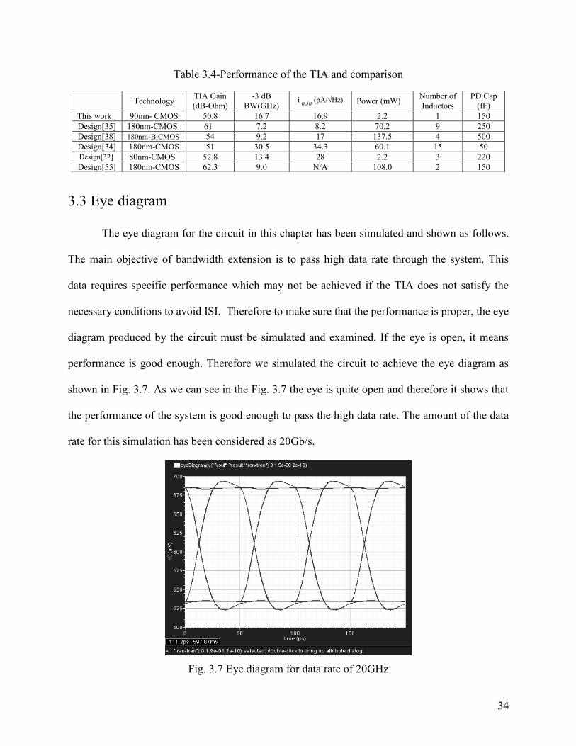
3.3 Eye diagram
The eye diagram for the circuit in this chapter has been simulated and shown as follows.
The main objective of bandwidth extension is to pass high data rate through the system. This
data requires specific performance which may not be achieved if the TIA does not satisfy the
necessary conditions to avoid ISI. Therefore to make sure that the performance is proper, the eye
diagram produced by the circuit must be simulated and examined. If the eye is open, it means
performance is good enough. Therefore we simulated the circuit to achieve the eye diagram as
shown in Fig. 3.7. As we can see in the Fig. 3.7 the eye is quite open and therefore it shows that
the performance of the system is good enough to pass the high data rate. The amount of the data
rate for this simulation has been considered as 20Gb/s.
Fig. 3.7 Eye diagram for data rate of 20GHz
Technology TIA Gain
(dB-Ohm) -3 dB
BW(GHz) i inn, (pA/√Hz) Power (mW)
Number of
Inductors
PD Cap
(fF) This work 90nm- CMOS 50.8 16.7 16.9 2.2 1 150
Design[35] 180nm-CMOS 61 7.2 8.2 70.2 9 250
Design[38] 180nm-BiCMOS 54 9.2 17 137.5 4 500
Design[34] 180nm-CMOS 51 30.5 34.3 60.1 15 50
Design[32] 80nm-CMOS 52.8 13.4 28 2.2 3 220
Design[55] 180nm-CMOS 62.3 9.0 N/A 108.0 2 150

35
3.4 Conclusion
In this chapter the zero pole cancellation for the inductive feedback technique for inverter
based transimpedance amplifier was shown mathematically and the process was proved by
detailed zero pole analysis. As an illustrative example the amount of photodiode capacitance was
chosen to be 150fF. Evaluation of the results shows that zero pole cancellation is the
phenomenon for bandwidth extension of the TIA. This method may be applied in mass
production of these circuits. However, because of mismatch problem, some extensive effort may
be required. The eye diagram for the circuit was also simulated and shown. The wide open eye
shows the success of the circuit to pass the high data rate without ISI and therefore with high
performance.
In the next chapter another mechanism of bandwidth extension using inductive feedback
for inverter based CMOS transimpedance amplifier is discussed. That is bandwidth extension
using compensation of the characteristics of complex conjugate poles.

36
Chapter 4
Bandwidth extension using complex conjugate
pole compensation
In chapter 3 the inductive feedback technique was detailed as an effective technique to
extend the bandwidth of the transimpedance amplifiers and the BW extension process was
explained. In the previous case the dominant pole of the system was cancelled using a newly
added zero by the inductive feedback and hence the bandwidth extension using the process of
zero-pole cancellation happened. The dominant pole of the system in that case is the pole
constructed by the photodiode capacitance (PD) since the value of the capacitance is such that

37
the pole concerned with that capacitance is the dominant pole in comparison with the other poles
in the system. Normally the dominant pole of a system can be constructed by large capacitances.
However, when we have a small photodiode capacitance in the system, we realize that in this
case there is no dominant pole constructed by the photodiode capacitance of the system. Even
though, we observe the extension of the bandwidth using the inductive feedback technique. For
the simplicity reasons we call the first case large PD and the second case small PD. In the case of
large PD the zero pole cancellation process happens whereas for the small PD case does not. In
this chapter [49] we will discuss the process of bandwidth extension for the case of the small PD
in detail. The feasibility of the process will be analyzed and the method will be confirmed
mathematically and by extensive simulations.
In this chapter the same TIA circuit using inductive feedback as chapter 3 is used. However,
instead of large PD (150fF) a small PD (50fF) is considered. It is shown that bandwidth
extension process is based on change in the characteristics of the complex conjugate poles.
4.1 Second order system
To explain the bandwidth extension process we will briefly look at the second order
system and its characteristics. Second order system with a pair of complex conjugate poles and
the mathematical characteristic of the poles and relations with frequency response are given as
follows. These relations shown in (4.1) are common equations for the second order system in
control system books [47].

38
22
2
2)(
nn
n
sssZ
(4.1)
Poles =-a± j b a, b>0 Poles= 21 nn j
22 ba
a
22 ban
BW= 1)21()21( 222 n
BWn )19.185.1( (for 0.3< <0.8)
In these relations and n are damping factor and natural frequency of the transfer function
Z(s). Poles of the system (roots of the denominator) have been shown in the relations. The -3dB
bandwidth of the transfer function is BW which has been calculated in the relation.
4.2 Complex conjugate poles compensation
Based on Fig. 4.1 which is the same as Fig. 3.2 in chapter 3 the transfer function of the
system is
Fig. 4.1 TIA with inductive feedback

39
DsCsBsA
csbsasZ
***
**)(
23
2
(4.2)
In which for the case of L=0 the coefficients are shown with the index 1 and we have:
01 a
fRcb 1
RGc m11
01 A
)(1 fiofoi ccccccRB (4.3)
)(1 mfofoioi GcgcgcRccC
mo GgD 1
Based on the transfer function the (delta) of the second order denominator is
11
2
1 4 DBC (4.4)
If we plug in the coefficients from the equations and simplify, we find boundary conditions as
2)1(
4
o
oi
Rg
GmRCC
(4.5)
If iC is large than this term the circuit will have a positive delta, therefore the circuit will
have real poles. In the case of negative delta the circuit will have a negative delta and therefore
the circuit will have complex conjugate poles. In this chapter we refer to the first case as large PD
and the second case as small PD.

40
In Fig. 4.1 for L≠ 0, we have the following coefficients
fLca 2
mf LGRcb 2
RGc m12 (4.6)
)(2 fiofoi ccccccLA
)()(2 mfofoifiofoi GcgcgcLccccccRB
)(2 mfofoioi GcgcgcRccC
mo GgD 2
In the case of small PD since the input capacitance is small based on Eq. (4.5) complex
conjugate poles exist. However, in the case of large PD real poles exist. In the case of small PD
these complex poles are the dominant poles of the circuit. By adding the inductor the coefficients
for the transfer function will change and therefore the characteristic of the poles will change and
the BW which is established based on these coefficients will change as well. We will explain this
mathematically in the following.
In a transfer function with two complex poles and one real pole, the denominator is a
third order polynomial as:
2223 )2()2( nnnn sss (4.7)
In this polynomial and n are damping factor and natural frequency of the complex conjugate
poles and is the real pole.

41
When the real pole is not dominant (i.e. is big) we can simplify the polynomial as:
223 2 nn sss (4.8)
In the case of L=0, we had a pair of complex conjugate poles with damping factor and natural
frequency as
1
1
1
11 5.0
D
B
B
C
1
1
1B
Dn (4.9)
)(1 fiofoi ccccccRB
)(1 mfofoioi GcgcgcRccC
mo GgD 1
After adding the inductor (applying the inductive feedback) we will have new damping factor
and natural frequency for the amplifier:
2
2
2
22 5.0
D
B
B
C
2
2
2B
Dn
(4.10)
)()(2 mfofoifiofoi GcgcgcLccccccRB
)(2 mfofoioi GcgcgcRccC
mo GgD 2
We can see that by adding the inductor we can control the damping factor and natural
frequency of the complex conjugate poles using the value of the inductor. Therefore by a judicial
choice of the value of the inductor we can extend the bandwidth.

42
4.3 Simulation results
In order to show the feasibility of the method, the circuit has been simulated using a well-
known sub-micron CMOS technology (i.e. 90nm CMOS STMicroelectronics). Simulations are
done with a single supply (i.e. Vdd =1.2 V) and in the presence of a 50fF photodiode capacitance
and 5fF loading capacitance. This loading capacitance is used to model an on-chip limiting
amplifier that would typically follow a TIA [46].
4.3.1 Zero-Pole Analysis
The zero pole analysis is performed using the schematic of the circuit (Fig. 4.1) with
ideal inductor. Based on the pole-zero analysis for the circuit when L=0 the circuit has two poles
and one zero and the poles are located in the LHP of the s-plane which shows the circuit is stable
[47]. For the case of L≠0 the circuit will have two zeros and three poles. Summary of the results
for zero pole analysis of the circuit is shown in table 4.1.
Table 4.1 Pole -Zero analysis for the circuit
L(nH) Zeros (GHz) Poles (GHz) Damping
Factor
Natural
Frequency (GHz)
Calculated
BW (GHz)
0 -20.1±13.5j 0.83 24.2
20.8
1
-56.8 -17.5±20.1j -52.4
0.65 26.6
28.6
2 -27.9
-10.6±20.7j -34.4
0.45
23.2 30.6
3 -18.5
-7.2±18.8j -30.6
0.36
20.1 28.5

43
4.3.2 Frequency response
The frequency response (TIA-Gain vs. Frequency) based on different values of the
inductor is shown in Fig. 4.2 and summarized in Table 4.2. These results are based on extracted
layout of the circuit in which the spiral inductor was modeled using typical models and values
available in the literature [48] as shown in Fig. 3.5 in chapter 3.
Fig. 4.2 Frequency response of the circuit

44
From Table 4.2 it can be seen that the -3dB bandwidth of 15.6GHz for L=0 was extended
using the inductive feedback technique to 29.7GHz. The power dissipation in this circuit is
2.2mW.
Table 4.2-AC simulation result of the TIA
M1(um) M2(um) R(Ohms) L(nH) G(dB-Ohms) BW(GHz) Peaking
12/0.1 12/0.1 400.7 0n 50.8 15.6 0
12/0.1 12/0.1 400.7 1n 50.8 29.7 0.6
12/0.1 12/0.1 400.7 2n 50.8 26.3 5.4
12/0.1 12/0.1 400.7 3n 50.8 23.5 7.5
In Table 4.3 we can see the comparison of this work with other previously published
works using other techniques. The circuit is very low power and compares favorably with other
works. The technique offers low-power dissipation, high bandwidth, using only one inductor.
Also noise performance in this circuit is competitive.
Table 4.3-Performance of the TIA and comparison
Technology TIA Gain
(dB-Ohm) -3 dB
BW(GHz) i inn, (pA/√Hz) Power (mW)
Number of
Inductors
PD Cap
(fF) This work 90nm- CMOS 50.8 29.7 13.5 2.2 1 50
Design[35] 180nm-CMOS 61 7.2 8.2 70.2 9 250
Design[38] 180nm-BiCMOS 54 9.2 17 137.5 4 500
Design[34] 180nm-CMOS 51 30.5 34.3 60.1 15 50
Design[32] 80nm-CMOS 52.8 13.4 28 2.2 3 220
Design[55] 180nm-CMOS 62.3 9.0 N/A 108.0 2 150

45
4.4 Eye diagram
The eye diagram for the circuit is simulated and shown in Fig. 4.3. The main objective of
bandwidth extension is to pass the data of high rate through the system without ISI. This high
data rate imposes specifications on the TIA. Therefore to make sure that the performance is
proper, the eye diagram produced by the circuit must be simulated and examined. If the eye is
open, it means performance is good enough. As we can see in the Fig. 4.3 the eye is quite open
and therefore it shows that the performance of the system is good enough to pass the high data
rate. For the inverter based TIA using inductive feedback in this simulation the amount of input
capacitance is 50fF. The amount of the inductor for this simulation is 1nH and the amount of
data rate is 40Gb/s.
Fig. 4.3 Eye diagram for the circuit for data rate= 40Gb/s

46
4.5 Estimation of BW Extension Ratio (BWER)
One of the important parameters to evaluate the Bandwidth extension techniques in
transimpedance amplifiers is theoretical bandwidth extension ratio (BWER). The definition for
this term is the comparison between the bandwidth before applying the technique to the circuit
and after applying the technique. The ratio of the new BW and the old BW will define the
BWER. The BW extension ratio can be found using simulations since the analytical calculation
of BWER can result on complicated and cumbersome equations and it has been avoided in the
literature. Because of the complexity of these analog systems when we face these kinds of
analyses, we have to make some assumptions. The discussion of the bandwidth extension ratio
for the two previously mentioned cases (i.e. large and small PD) were done and will be reported
in this part.
The analysis for BWER for the Inductive Feedback technique shows that for the first case
(large PD) where the zero-pole cancellation process is done the theoretical BWER is
approximately 2.7. For the second case (small PD) in which the BW extension process happens
based on the change in the characteristics of the complex conjugate poles BWER is
approximately 2.1. These figures of merits are competitive in comparison with other Bandwidth
extension techniques which will be discussed in this chapter.

47
4.5.1 BWER for large PD
The process for bandwidth extension in this case is zero pole cancellation. The circuit
before adding the inductor has two poles in which one of the poles is dominant and by adding the
inductor the dominant pole will be cancelled and the circuit will be left by a pair of complex
conjugate poles. In order to find the theoretical BWER we need to mathematically plot the
transfer functions of the systems before and after applying the technique.
The BWER based on the mathematical formula of the transfer function and typical values for the
circuit parameters has been shown in Fig. 4.4.
Fig. 4.4 Mathematical simulation of transfer function
From Fig. 4.4 with L=0 and L=1nH the values for the -3dB bandwidth are 165Grad/s and
455Grad/s. Therefore theoretical BWER of more than 2.7 can be achieved using this technique.

48
4.5.2 BWER for small PD
In this case the coefficient C1 is small and therefore the magnitude of this pole will be
large which means the real pole of the transfer function is not dominant. Therefore the BW
extension will happen using the inductive feedback by changing the characteristics of the
dominant poles (complex conjugate poles).
In this case the circuit already has a pair of complex conjugate poles. Based on the transfer
function, damping factor and natural frequency can be found using these relations
1
1
1
15.0D
B
B
C
1
1
B
Dn (4.15)
)(1 fiofoi ccccccRB
)(1 mfofoioi GcgcgcRccC
mo GgD 1
Based on the damping factor and the natural frequency we can calculate the -3dB bandwidth
from
BW= 1)21()21( 222 n (4.16)
We can approximately assume that the complex conjugate poles construct the frequency
response of the circuit which is not very far from reality.
2
2
2
25.0D
B
B
C
2
2
B
Dn (4.17)

49
)()(2 mfofoifiofoi GcgcgcLccccccRB
)(2 mfofoioi GcgcgcRccC
mo GgD 2
Based on the damping factor and the natural frequency we can calculate the -3dB bandwidth
from the relation
BW= 1)21()21( 222 n (4.18)
For the PD=50fF the same process was done and the result was shown in Fig. 4.5.
Fig. 4.5 Mathematical simulation of transfer function

50
The theoretical bandwidths based on values of inductors of L=0 and L=0.75nH are
276Grad/s and 556Grad/s respectively. It is shown in Fig. 4.5 that the theoretical BWER of more
than 2 can be achieved when the input capacitance is small.
The bandwidth reported in this part is the Matlab simulation of the transfer function of
the small signal model using ideal inductors with no parasitic elements [76]. In this simulation
the input capacitance is only considered to be the photodiode capacitance and the feedback
capacitances from input and output are ignored. This is the reason the bandwidth reported in this
part is more than the bandwidth reported from the actual bandwidth from extracted simulation.
4.6 Conclusion
In this chapter the theory of Bandwidth extension for small value of Photodiode (PD) was
explained by means of approximately considering the complex conjugate poles as dominant
poles of the circuit. The behavior of the circuit can be realized by explaining that the
characteristics of the complex conjugate poles are changed using the inductive feedback in order
to extend the bandwidth. The circuit achieves -3dB bandwidth of almost 30 GHz by only using
one inductor when draws 2.2mW. The eye diagram of the system has been simulated to show the
effectiveness of the circuit to pass the high data rate without ISI. In addition to that the
discussion of theoretical BWER for both the cases of large and small Photodiode (PD) was
shown. For the case of the large PD, BWER of more than 2.7 was achieved and for the case of
the small PD, BWER of more than 2. These results are competitive with other techniques. Shunt
peaking achieved the BWER of 1.7 [30] and that for inductor between the stages is 2.4 [37]. PIP
technique achieved 3.3 [34] and that for series peaking is 2.5 [35].

51
In chapter 3 inductive feedback was used to extend the BW (zero-pole cancellation) when
dominant pole was at the input of the circuit (large PD). In this chapter the other case was
discussed when the input pole is not dominant and BW extension is done by changing the
characteristics of the complex conjugate poles. The inductive feedback technique based on the
analysis and simulation results shows that, it is capable of extending the BW effectively without
reducing the DC gain.
In the next chapter another topology of transimpedance amplifiers using inductive
feedback will be analyzed. The process of bandwidth extension for common source based
transimpednace amplifier will be discussed and a new 3 stage TIA will be introduced.
52
Chapter 5
Wideband Common Source based TIAs
Optical receivers have a great role in today’s high data rate (Gb/s) wireline data
communication systems. To achieve such high data rate all the amplifiers in the signal path should
be wideband enough to be able to amplify the signals in those high frequencies. Transimpedance
amplifiers (TIAs) at the frontend of the optical receivers have the important task of amplifying the
small current received from the photodiode to an acceptable level of voltage for the next stage.
The bandwidth of CMOS TIAs is limited by the photodiode (PD) capacitance and parasitic

53
capacitances of the MOS transistors. Attempts have been made recently to extend the bandwidths
of TIAs to reach the data rate of 100Gb/s. In this chapter an attempt has been made to extend the
bandwidth of cs-based TIA using inductive feedback more by introducing a new three- stage TIA
to achieve data rates of more than 40Gb/s.
In this chapter, inductive feedback approach for BW extension of common source based
Transimpedance amplifier has been applied [39]. The effect of parasitic capacitances [51] of the
MOS transistor has been reduced using the mentioned approach. The process of zero-pole
cancellation for 3 different values of the photodiode capacitance (CPD) to extend the BW of the
amplifier is explained. A new and very wideband three stage transimpedance amplifier based on
common source amplifier is introduced. To demonstrate the feasibility of the technique
transimpedance amplifiers are simulated in a well-known CMOS technology (i.e. 90nm
STMicroelectronics).
Single stage common source based transimpedance amplifiers achieve 3-dB bandwidths of
32.1GHz, 21.8GHz, and 15.8GHz in the presence of a 50fF, 100fF, 150fF photodiode
capacitances and 5fF loading capacitance while only dissipating 2.03mW. The new three stage
amplifier achieves bandwidths of 42.8GHz, 35.5GHz, and 28.5GHz in the presence of 50fF,
100fF, 150fF photodiode capacitances. The power consumption for the new transimpedance
amplifier is 6.1mW. For all the structures noise performance is competitive in comparison with
other works. Eye diagrams for single stage and three stage transimpedance amplifiers have been
simulated and shown in this chapter.

54
5.1 Single stage common source based TIA using inductive feedback
The idea in this part is to extend the bandwidth of the TIA by deliberately adding a zero to
the transfer function of the TIA and hence cancel the dominant pole of the amplifier thereby
extending the BW. This can be done by adding an inductor to the feedback path of the TIA. The
newly introduced inductor in the feedback path (inductive feedback) adds one zero and one pole
to the transfer function of the TIA and by an appropriate design the newly added zero can cancel
the dominant pole of the amplifier and hence extend the BW [44].
In order to discuss the technique in detail we consider two TIAs shown in Figures 5.1 and
5.2. In this chapter we refer to the circuit in Fig. 5.1 as the common source based TIA (CS-based)
[78] with resistive feedback and the circuit in Fig. 5.2 as the common source TIA with inductive
feedback [44], [39].
The small signal model for the single stage common source based TIA with inductive
feedback is shown in Figure 5.3. The parasitic capacitances of the transistor are shown in this
figure as well. This small signal model is used to derive the mathematical transfer function of the
circuits. This mathematical model is used to analyze the circuits in this chapter.

55
Fig. 5.1 CS-TIA with resistive feedback
Fig. 5.2 CS-TIA with inductive feedback
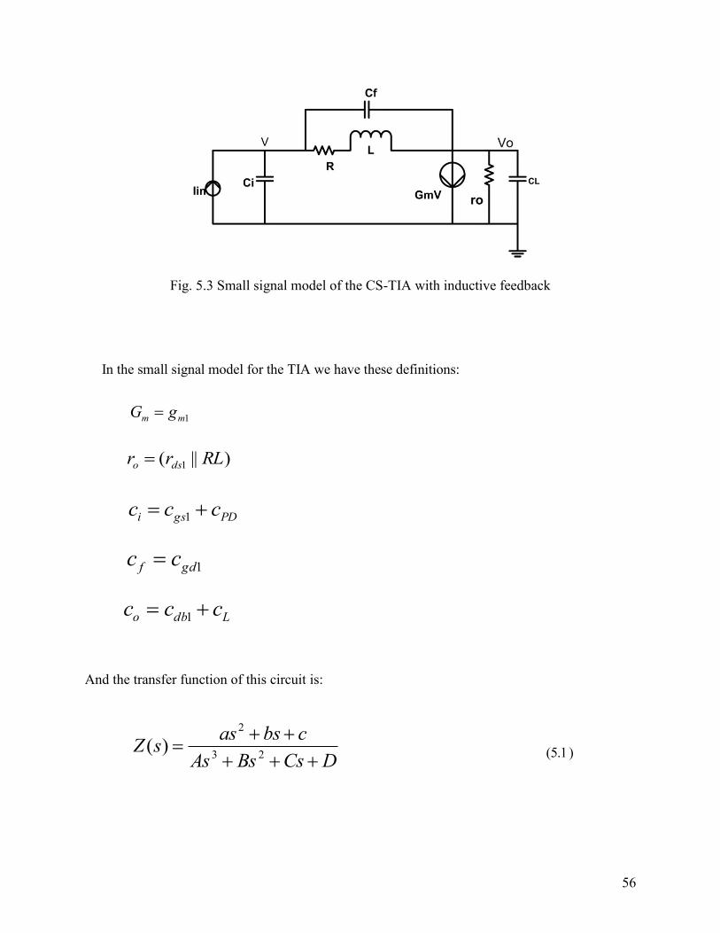
56
Fig. 5.3 Small signal model of the CS-TIA with inductive feedback
In the small signal model for the TIA we have these definitions:
1mm gG
)||( 1 RLrr dso
PDgsi ccc 1
1gdf cc
Ldbo ccc 1
And the transfer function of this circuit is:
DCsBsAs
cbsassZ
23
2
)(

57
In which for the case of the Figure 5.1 (L=0) the coefficients are shown with the index 1 and
we have:
01 a
fRcb 1
RGc m11
01 A
)(1 fiofoi ccccccRB
)(1 mfofoioi GcgcgcRccC
mo GgD 1
For the case of the circuit in Figure 5.2 we have the coefficients as (shown with the index 2):
fLca 2
mf LGRcb 2
RGc m12
)(2 fiofoi ccccccLA
)()(2 mfofoifiofoi GcgcgcLccccccRB
)(2 mfofoioi GcgcgcRccC

58
mo GgD 2
Considering the transfer function of the system in Figure 5.1, the dominant pole of the system
which defines the -3db BW, can be approximately calculated as D1/C1 which is
)( mfofoioi
mo
GCgCgCRCC
GgP
(5.2)
In this approach, the dominant pole is cancelled by introducing a new zero to the transfer
function. This can be achieved by adding an inductor in the feedback path of the amplifier of Fig.
5.1 which results in Figure 5.2. As we can see adding an inductor to the feedback path adds one
pole and one zero to the transfer function and the amount of newly added zero is approximately
L
RZ (5.3)
From the equations (5.1) and (5.2) by choice of the inductance we can cancel the dominant
pole of the circuit in Figure 5.1 hence extend the BW. An approximate value for the amount of the
inductor can be calculated by solving the equation P=Z so we will have
mo
mfoioi
Gg
GCgCRCCRL
)()( 2
(5.4)

59
5.2 Zero-Pole Cancellation Process
In order to show the bandwidth extension process in detail the circuit has been simulated
using a well-known sub-micron CMOS technology (i.e. 90nm CMOS STMicroelectronics).
Simulations are done with a single supply (i.e. Vdd=1.2 V). To show the validity of the zero-pole
cancellation process for BW extension, the simulations were done for 3 different PDs of
50,100,150fF. The load capacitance for these 3 circuits is 5fF. This loading capacitance is used to
model an on-chip limiting amplifier that would follow a TIA.
Based on the pole-zero analysis for the circuit in Figure 5.1 (TIA with resistive feedback),
the circuit has two poles and one zero and the poles are located in the LHP of the s-plane which
shows the circuit is stable. Considering the case in Figure 5.2 in which we have added the
inductor to the feedback, the circuit will have two zeros and three poles. By choosing the inductor
according to (5.4) we can cancel the dominant pole leaving a pair of complex conjugate poles in
the circuit. The circuit after having cancelled the single dominant pole will have two complex
conjugate poles with a damping factor and natural frequency which can be designed for the
desired frequency response. The zero-pole cancellation processes are shown in the tables 5.1, 5.2,
5.3 for CPD of 50,100,150fF and we can see that by changing the value of the inductor in the
circuit the newly added zero is moving towards the dominant pole of the circuit. In the end it
reaches to that pole and cancels it and hence this zero can extend the -3dB BW. We can also see
that the positions of the complex conjugate poles are changing by sweeping the value of the
inductor.

60
Table 5.1 Pole -Zero analysis for the circuit (PD=50fF)
L(nH) Zeros (GHz) Poles (GHz)
0 -15.5
-60.9
1
-50.5
-19.6
-45.4±32.3j
1.5
-33.1
-23.7
-32.7±25.1j
1.8
-27.4
-27.4
-27.8±22.1j
2
-24.7
-31.6
-23.4±20.1j
In the table 5.1 for the inductor amount of 1.8nH the pole and the zero of the circuit
become equal and zero pole cancellation happens for that value of the inductor. In this case the
complex conjugate poles will construct the -3dB bandwidth of the circuit.

61
Table 5.2 Pole -Zero analysis for the circuit (PD=100fF)
L(nH) Zeros (GHz) Poles (GHz)
0 -8.3
-63.6
1
-50.4
-9.1
-48.9±35.9j
3
-16.4
-13.1
-25.7±13.8j
3.25
-15.1
-15.1
-24±10.9j
3.5
-13.9
-20.3
-20.5±6.9j
In table 5.2 for the inductor amount of 3.25nH the pole and the zero of the circuit become equal
and zero pole cancellation happens for that value of the inductor.

62
Table 5.3 Pole-Zero analysis for the circuit (PD=150fF)
L
(nH)
Zeros
(GHz)
Poles
(GHz)
0 -5.6
-64.1
2
-24.6
-6.1
-33.7±25.7j
4
-12.2
-8.2
-24.7±9.1j
4.5
-10.2
-10.2
-23.5±2.8j
5
-9.7
-30.4
-12.2±2.1j
We can see that in the table 5.3 for the inductor amount of 4.5nH the pole and the zero of
the circuit become equal and zero pole cancellation happens for that value of the inductor.
In the tables 5.1, 5.2 and 5.3 zero pole cancellation process for the single stage common
source based transimpedance amplifier for different values of photodiode capacitance were
shown. In these tables the exact value of the inductor showing the process can be found.
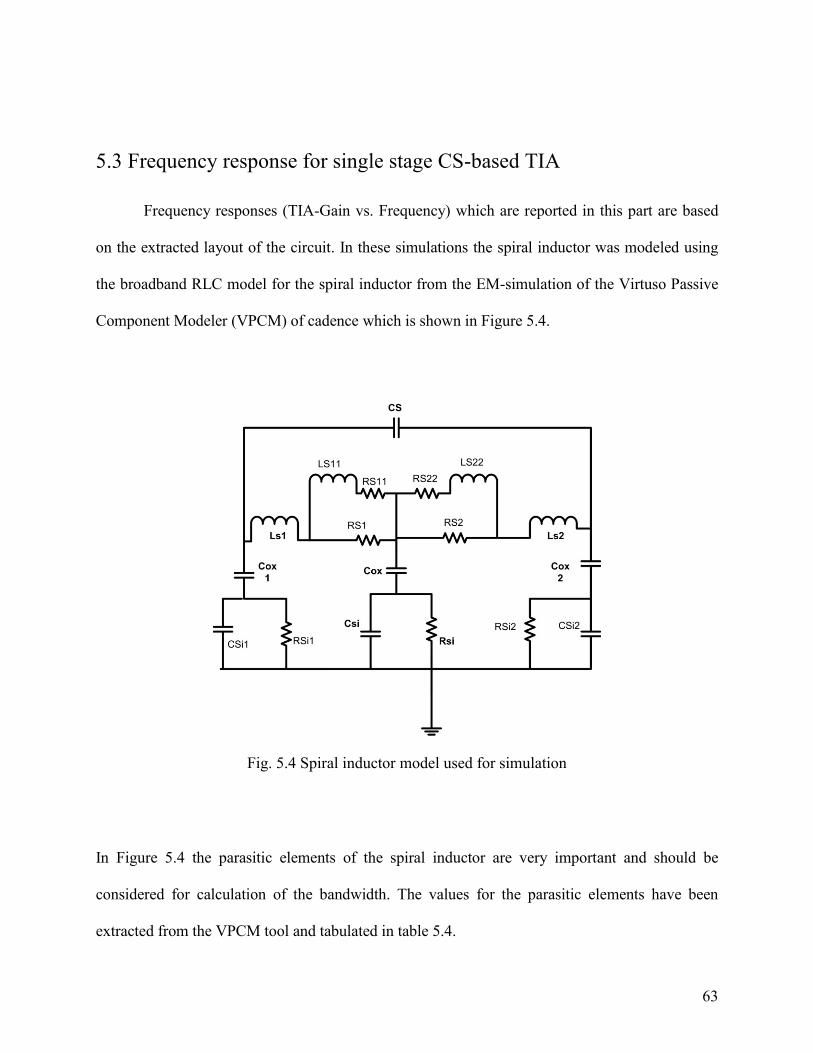
63
5.3 Frequency response for single stage CS-based TIA
Frequency responses (TIA-Gain vs. Frequency) which are reported in this part are based
on the extracted layout of the circuit. In these simulations the spiral inductor was modeled using
the broadband RLC model for the spiral inductor from the EM-simulation of the Virtuso Passive
Component Modeler (VPCM) of cadence which is shown in Figure 5.4.
Fig. 5.4 Spiral inductor model used for simulation
In Figure 5.4 the parasitic elements of the spiral inductor are very important and should be
considered for calculation of the bandwidth. The values for the parasitic elements have been
extracted from the VPCM tool and tabulated in table 5.4.

64
Table 5.4 Typical Values of the parasitic elements
Cs
Ls1
Rs1
Ls11
Rs11
Ls2
Rs2
Ls22
Rs22
Cox1
Cox
Cox2
Csi1
Rsi1
Csi
Rsi
Csi2
Rsi2
2.5 fF
1 nH
6.7 Ohms
176 pH
6.4 Ohms
1 nH
6.7 Ohms
176 pH
6.4 Ohms
6.5 pH
17.5 fF
5.1 fF
14.8 fF
641.6 Ohms
19.2 fF
493.8 Ohms
5.5 fF
1.7 KOhms
The frequency responses based on different values of the inductor are shown in Figures
5.5, 5.6, 5.7. In these figures two cases are shown. One case is the simulation for the frequency
response without the inductor L=0 and the other case is with the value of the inductor which gives
the bandwidth extension for the respective photodiode capacitance. Fig. 5.5 shows the simulation
for the photodiode capacitance of 50fF for which the value of the inductor is 2nH.
Fig. 5.5 Frequency response of the CS-TIA (PD=50fF)

65
Fig. 5.6 shows the simulation for the photodiode case of 100fF for which the value of the
inductor is 3nH. Fig. 5.7 shows the simulation for the photodiode capacitance of 150fF for which
the value of the inductor is 5nH. In each case the extension of the bandwidth can be observed.
Fig. 5.6 Frequency response of the CS-TIA (PD=100fF)

66
Fig. 5.7 Frequency response of the CS-TIA (PD=150fF)
The frequency responses are summarized in Tables 5.5, 5.6, 5.7. The amount of gain peaking
has been shown as well. From each table it can be observed that the bandwidth has been extended
from the value when L=0 to the value of that when L is not 0.

67
Table 5.5 AC simulation result of the TIA (CPD=50fF)
M1 R(Ohms) RL(Ohms) L(nH) G(dB-Ohms) BW (GHz) Peaking(dB)
12/0.1 400 400 0n 46.8 8.05 0
12/0.1 400 400 2n 47.1 21.8 0
Table 5.6 AC simulation result of the TIA (CPD=100fF)
Table 5.7 AC simulation result of the TIA (CPD=150fF)
M1 R(Ohms) RL(Ohms) L(nH) G(dB-Ohms) BW (GHz) Peaking(dB)
12/0.1 400 400 0n 46.8 5.6 0
12/0.1 400 400 5n 47.1 15.8 0
From tables it can be seen that Bandwidth Extension Ratio (BWER) of more than 2 has been
achieved. The technique offers low power dissipation, high bandwidth, using only one inductor.
M1 R(Ohms) RL(Ohms) L(nH) G(dB-Ohms) BW (GHz) Peaking(dB)
12/0.1 400 400 0n 46.8 14.1 0
12/0.1 400 400 3n 47.1 32.1 0

68
5. 4 Three Stage Common Source based Transimpedance amplifier
Cascaded amplifiers are one of the most common ways to widen the bandwidth of the
amplifiers [37] and therefore, we can cascade the common source transimpedance amplifiers to
get more Gain*Bandwidth from the amplifier. In this part we introduce cascaded three stage
common source Transimpedance amplifier with inductive feedback as a very wideband structure
for high speed optical receivers. Figure 5.8 shows this new TIA. As can be seen in the circuit
three single stage common source TIAs using inductive feedback have been cascaded together to
build a new TIA.
Fig 5.8 Three stage common source TIA using inductive feedback

69
In figures 5.9, 5.10, 5.11 we can see the frequency response for the three-stage TIA for
different values of the inductors for the photodiode capacitances (PD) of 50fF, 100fF, 150fF
respectively. The bandwidth for bigger values of the Photodiode is lower.
Fig 5.9 Frequency response of the three stage TIA (PD=50fF)

70
Fig 5.10 Frequency response of the three stage TIA (PD=100fF)
Fig 5.11 Frequency response of the three stage TIA (PD=150fF)

71
In tables 5.8, 5.9, 5.10, we can see the summary of the frequency response results
(bandwidth, gain, and gain peaking) of the three stage TIA for different values of the photodiode
capacitance. In the table 5.8 the results for the PD of 50fF is shown. From the table we can see
that the -3dB bandwidth has been extended from 10.7GHz to 42.8GHz and this corresponds to
BWER (Bandwidth Extension Ratio) of more than 4 for this circuit. In the table 5.9 the results
for the PD of 100fF are shown. The -3dB bandwidth for this case has been extended from
6.2GHz to 35.5GHz. This corresponds to BWER of around 6. In the table 5.10 for the PD of
150fF the bandwidth from 4.2 GHz for the case of resistive circuit (all L=0) has been extended to
28.5GHz which corresponds to BWER of 7.
Table 5.8 Three Stage CS based TIA with inductive feedback (CPD=50fF)
L1
(nH)
L2
(nH)
L3
(nH)
Gain
(dB-ohms)
BW
(GHz)
Peak
(dB)
2 2 2 46 42.8 2.7
0 0 0 42.9 10.7 0

72
Table 5.9 Three stage CS TIA with inductive feedback (CPD=100fF)
L1
(nH)
L2
(nH)
L3
(nH)
Gain
(dB-ohms)
BW
(GHz)
Peak
(dB)
3 3 3 46.5 35.5 1.9
0 0 0 42.9 6.2 0
Table 5.10 Three stage CS TIA with inductive feedback (CPD=150fF)
L1
(nH)
L2
(nH)
L3
(nH)
Gain
(dB-ohms)
BW
(GHz)
Peak
(dB)
5 5 5 48.1 28.5 2.1
0 0 0 42.9 4.2 0
These results show the effectiveness of the technique for bandwidth extension for
different values of the photodiode capacitance (CPD). By adjusting the value of the second
resistor the amount of the gain peaking can be adjusted. For the case of 50fF, 100fF, 150fF R2
can be 700 ohms, 800Ohms and 1.5Kohms respectively to mitigate the peaking.

73
5.5 Noise Analysis
The input referred noise current In, in is an important issue for TIA design, which
determines the sensitivity of the circuit. Also in cascaded structures normally the effect of the
first stage in the noise performance of the whole chain can be very important because the impact
of the noise from other stages can be mitigated through the gain of the previous stages. As for the
noise analysis of the CS-stage, studies show that noise characteristics of the device are
dominated by the drain thermal noise [52], [53]. Based on the discussion above we can model the
input referred noise based on the equivalent model for the noise performance for this circuit
which has been shown in the Figure 5.8.
Fig 5.12 Noise equivalent model of the CS-TIA
In order to analyze the input referred noise first we define the noise sources in the equivalent
circuit.

74
KTRV Rn 4,2
LRLn KTRV 4,2 (5.5)
141,
2
mMn gKTI
The value for is approximately mentioned as 2/3 and the exact amount for this parameter is
under active research [54]. In order to analyze this, we can apply the superposition to noise
sources and the result of the noise analysis will be the summation of the current noise at the
input. We can approximately write the relation for the input referred noise as
R
KT
Zg
ZCgKTI
Rm
RPD
minn
4)(14
22
22
,2
1
1
(5.6)
LsRZR
Based on the above equations, the inductive feedback technique can improve the noise
performance of the transimpedance amplifier. The reason is that the inductive feedback makes a
frequency dependent feedback factor which reduces the effect of the noise sources in the circuit.

75
It can be shown that the noise contribution from the load is very small. For the matter of
simplicity we ignore the noise effect of the output load to the input. In equation (5.5) for the case
of regular TIA (L=0) by increasing frequency only the numerator will increase and hence the
noise current will increase. However, for the case of inductive feedback the term including the
frequency appears in the denominator as well which decreases the noise contribution referred to
the input of TIA. Simulations for the noise analysis are done on the circuit and the results can be
seen in figures 5.13 and 5.14. Figures show the results for the one stage and also 3 stage CS-
Based TIAs.
In Fig. 5.13 the simulations for the input referred noise of the single stage common
source based transimpedance amplifier are shown. Simulations for different values of the
photodiode capacitances and respective values of the inductors can be seen in this figure.
The discussion in this part is related to noise PSD. In each case, it can be observed that
adding the inductor to the feedback path can improve the noise performance of the circuit.
.

76
Fig 5.13 Simulated In, in with different values of Cpd and L for one stage CS TIA
In Fig. 5.14 the simulations for the input referred noise of the three stage common source
based transimpedance amplifier are shown. Simulations for different values of the photodiode
capacitance and respective values of the inductors can be seen in this figure.
The simulation shows the noise PSD. For each case, it can be observed that adding the
inductor to the feedback path can improve the noise performance of the circuit.

77
Fig 5.14 Simulated In, in with different values of Cpd and L for three stage CS TIA
In table 5.11 we can see summary of the results and comparison with other works. The
first six rows show the results from this chapter. The single stage and the three stage common
source TIA with inductive feedback for 3 different values of the photodiode capacitance have
been simulated and the results for the circuitries of this chapter are compared in this table. As we
can see the circuits are very low power in comparison with other works. Despite having low
power the circuits have competitive noise performance. There is no figure of merit [74] which
can define all the parameters involved with the design of the transimpedance amplifiers. In this
table, it can be seen the circuits in this chapter are low power and high bandwidth in comparison

78
with other previously published works. The number of inductors used in the circuits in this
chapter is lower than the number of inductors of most of the TIAs.
Table 5.11 Summary of the results and comparison with other works
Technology
TIA Gain
(dB-Ohm)
-3 dB
BW(GHz)
i inn, (pA/√Hz) Power (mW)
Number of
Inductors
PD Cap
(fF)
This work
[Fig. 5.8]
90nm-CMOS 42.9 42.8
29.8 6.1 3 50
This work
[Fig. 5.8]
90nm-CMOS 42.9 35.5
33.5 6.1 3 100
This Work
[Fig. 5.8]
90nm-CMOS 42.9 28.5
38.4 6.1 3 150
This work
[Fig. 5.2]
90nm- CMOS 47.1 32.1 15.6
2.03 1 50
This work
[Fig. 5.2]
90nm- CMOS 47.1 21.8 17.3
2.03 1 100
This work
[Fig. 5.2]
90nm- CMOS 47.1 15.8 19.4
2.03 1 150
Design[44] 90nm-CMOS 50.8 16.7 16.9
2.2 1 150
Design[35] 180nm-CMOS 61 7.2 8.2 70.2 9 250
Design[37] 180nm-BiCMOS 54 9.2 17 137.5 4 500
Design[34] 180nm-CMOS 51 30.5 34.3 60.1 15 50
Design[32] 80nm-CMOS 52.8 13.4 28 2.2 3 220
Design[55] 180nm-CMOS 62.3 9.0 N/A 108.0 2 150
Design[39] 65nm-CMOS 8 29GHz N/A 6mW 1 N/A

79
5.6 Eye diagram
The eye diagram for the circuit in this chapter has been simulated and shown as follows.
The main objective of bandwidth extension is to pass high data rate. This data requires specific
performance which may not be achieved if the TIA does not satisfy the necessary conditions to
avoid ISI. Therefore to make sure of the performance, the eye diagram produced by the circuit
must be simulated and examined. If the eye is wide open, it shows performance is good.
Fig 5.15 shows the eye diagram for the three stage common source based
Transimpedance amplifier using inductive feedback with input capacitance of 50 fF. In this
simulation the value of L is 2nH the data rate of is 50Gb/S.
Fig. 5.16 shows the eye diagram for the one stage common source based transimpedance
amplifier using inductive feedback and for the input capacitance of 50fF. In this simulation the
data rate of 40Gb/s and L of 2nH have been used.
As we can see in these figures the eye is quite open and therefore it shows that the
performance of the system is good enough to pass the high data rate.
In comparison between the two topologies, simulations show that the one stage
transimpedance amplifier is incapable of passing the data rate of 50Gb/s without inter symbol
interference in opposed to the three stage amplifier.

80
Fig. 5.15 Eye diagram for the three-stage TIA (data rate=50Gb/s)
Fig. 5.16 Eye diagram for the one stage CS-TIA (data rate=40Gb/s)
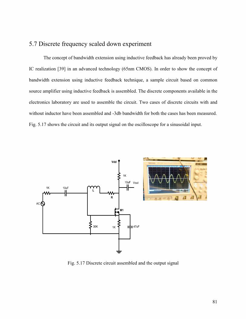
81
5.7 Discrete frequency scaled down experiment
The concept of bandwidth extension using inductive feedback has already been proved by
IC realization [39] in an advanced technology (65nm CMOS). In order to show the concept of
bandwidth extension using inductive feedback technique, a sample circuit based on common
source amplifier using inductive feedback is assembled. The discrete components available in the
electronics laboratory are used to assemble the circuit. Two cases of discrete circuits with and
without inductor have been assembled and -3db bandwidth for both the cases has been measured.
Fig. 5.17 shows the circuit and its output signal on the oscilloscope for a sinusoidal input.
Fig. 5.17 Discrete circuit assembled and the output signal

82
First, the circuit has been assembled without the inductor (L=0) and with the resistor value
of 100 Ohms. The -3dB cut-off frequency for this case is 22MHz. Then, the circuit is assembled
by adding the inductor to the feedback path. The value of the inductor which has been added to
the feedback path is L=100uH. In this case the measured -3dB cut-off frequency is 35MHz. This
experiment confirms that by adding the inductor to the feedback path the bandwidth of the circuit
is extended from 22MHz to 35MHz. This shows the technique can extend the bandwidth of the
transimpedance amplifier. In Fig. 5.18 the frequency response based on the experiment is shown.
The effect of loading of the oscilloscope has been considered in calculating the transimpedance
gain.
Fig. 5.18 Frequency response based on discrete experiment
Blue: without inductor
Red: with inductor
83
The reason for dropping the gain of amplifier at high frequencies is parasitic capacitances
of the transistor. The value of the impedance for a capacitance is related inversely to the
frequency. By increasing the frequency, the impedance values for these capacitances decrease.
Therefore these low impedance values can lower the gain of the amplifier at high frequencies. In
the second circuit the inductor is added to the feedback path (L≠0). The value of the impedance
for the inductor is proportional to the value of the frequency as opposed to impedance value of
capacitor. Therefore this impedance which is increasing by higher frequencies compensates the
impedance of the parasitic capacitances of the circuit. Therefore, this compensation of the
impedance results in rolling off the gain not as fast as the case when L=0. This will result in the
extension of the bandwidth. In this thesis it was shown that this inductor added a zero to the
transfer function of the circuit. By adding a zero to the transfer function, the slope of the
frequency response in the Bode plot can be compensated by 20dB. A pole which was created by
capacitance of transistor drops the slope of the frequency response by -20dB. These phenomena
will lower the pace at which the gain rolls off. Therefore as a result of adding the inductor to the
feedback path the -3dB bandwidth will be extended.
5.8 Conclusion
In this chapter the inductive feedback technique is applied to the CS-based TIA. The
process of zero pole cancellation for single stage CS-based transimpedance amplifier is
explained mathematically using the small signal model and transfer function. Simulation results
for frequency response are shown. HSpice zero-pole analysis is performed for different values of

84
the indcuotrs and photodiode capacitances (PD). In each case the process of zero pole
cancellation is analyzed. A 90nm CMOS process from STMicroelectronics is used to simulate
these circuits. A new three stage very wideband transimpedance amplifier based on the common
source TIA with inductive feedback is introduced. The simulation results for the frequency
response of the new TIA are shown. The new TIA offers high bandwidth for very low power
consumption. Based on the theory of the cascaded amplifiers, this circuit can have higher
Gain*Bandwidth than the single stage TIA. The combination of the inductive feedback technique
and the cascaded amplifiers can offer high BWER for these types of circuits. Eye diagrams for
the one stage and three stage circuits have been simulated and shown in this chapter. For high
data rates used in the simulation the eye is wide open for both the single stage and three stage
TIA. The open eye proves the capability of the circuit to pass the high data rate without
significant inter symbol interference (ISI). Noise analysis for single stage and three stage
transimpedance amplifiers for different values of photodiode capacitances and inductors are done
using 90nm CMOS STMicroelectronics. A sample of a frequency scaled down of the circuit has
been assembled and the measurement results are shown for this circuit. The evaluation of the
results shows the effectiveness of the technique to extend the bandwidth of the TIAs effectively.
In the next chapter the conclusions and contributions of the thesis and future works are
explained. Detailed contributions to knowledge of this thesis are explained. Insights for the
future work based on this thesis and also for other horizons in the field of TIAs are given.

85
Chapter 6
Conclusion
6.1 Conclusions and contributions of the thesis
Optical receivers have an important role in high data rate data communication systems.
These receivers have data rates of multi Gb/s. To achieve such high data rate in the design of
optical receivers, we need wideband amplifiers in the signal path. As a rule of thumb, the
bandwidth of the amplifiers in the optical receivers should be 70% of the data rate. For these
systems, CMOS technology is used which is the only candidate that can achieve the required
level of integration with reasonable cost.

86
The small current received from the photodiode is amplified using the transimpedance
amplifier which is one of the main building blocks in the receiver frontend. Due to high data rate
of fiber optic communication systems the bandwidth of transimpedance amplifiers should be
high and it should satisfy gain requirements.
It had been shown that inductive feedback technique was capable of extending the
bandwidth of CMOS transimpedance amplifiers effectively [39]. However, no mathematical
analysis was available in the literature explaining this phenomenon. The main focus of this thesis
was to explain mathematically the mechanism of bandwidth extension of CMOS transimpedance
amplifiers with inductive feedback.
The analysis of zero pole cancellation for bandwidth extension of transimpedance
amplifiers was discussed in detail and simulation results for this technique was given [44].
Another analysis for the inductive feedback technique which is based on complex conjugate pole
compensation for the bandwidth extension of the transimpedance amplifiers was shown in detail
as well [49]. When PD is small, the total input capacitance of the amplifier is so small that it
does not construct the dominant pole of the amplifier. In this thesis, it was shown that for small
PD how inductive feedback could change the characteristic of the complex conjugate poles of the
transfer function and hence extend the bandwidth of the TIA [49].
First, we applied the inductive feedback to an inverter type amplifier and showed that this
technique was effective to extend the bandwidth. Then, we applied the technique to common
source amplifier with a resistive load and showed the bandwidth extension process of zero pole
cancellation [56]. In this thesis a new three stage transimpedance amplifier which was based on
cascading [50] the common source amplifier was introduced as well.

87
Normally to design Ultra Wideband (UWB) amplifiers [73], only one amplification stage
is not enough. In fact, to design a very high bandwidth amplifier, a combination of bandwidth
extension techniques is used. Combination of the inductive feedback technique with other
techniques was the idea which could lead to new and very wideband transimpedance amplifier.
First the zero pole cancellation process for the single stage amplifier in which the inductive
feedback technique had been applied was discussed in detail for 3 values of the photodiode
capacitances of 50fF, 100fF, and 150fF. Next the new transimpedance amplifier which was the
three-stage common source based amplifier was introduced. The process of bandwidth extension
has been discussed and shown using extensive simulation [50],[56]. Moreover, the noise
analyses for both single stage and three-stage amplifiers for different values of the photodiode
capacitance i.e. 50fF, 100fF, and 150fF were shown in detail. The noise performance was shown
to be improved using the inductive feedback technique for transimpedance amplifiers. In
addition, eye diagrams for each transimpedance amplifier were simulated and shown. Wide open
eyes for the structures prove the capability of the circuitries to accommodate high data rate. A
discrete frequency scaled down sample circuit was built and the results were given to prove the
concept of bandwidth extension.
Major contributions of this thesis are:
Mathematical analysis of zero pole cancellation for the inverter based CMOS
transimpedance amplifier [44]
Mathematical analysis of bandwidth extension by compensation of complex conjugate
pole characteristics [49]

88
Mathematical analysis of bandwidth extension for common source based
transimpednace amplifiers with different input capacitances based on zero pole
cancellation [56]
Introduction of a new three stage CMOS transimpedance amplifier based on common
source stages using inductive feedback
Overall, this thesis provides insight and develops useful techniques to design high speed
optical receivers using CMOS integrated circuit technology. It gives detailed understanding
of mechanisms of bandwidth extension for tansimpedance amplifiers and emphasizes on
understanding these details which have been usually ignored in the literature.
6.2 Future work
In this thesis one of the effective methods to extend the bandwidth of transimpedance
amplifiers was taken into account. Detailed analysis for bandwidth extension of transimpedance
amplifiers using this technique was performed by mathematical analysis and extensive
simulation. Same method can be applied to other bandwidth extension techniques. Deep
understanding of these processes can help researchers to move forward towards better designs in
different aspects.
The three stage transimpedance amplifier circuit was introduced in this thesis and
effectiveness of the circuitry to extend the bandwidth of transimpedance amplifier was shown.
For the newly introduced transimpedance amplifier (cascaded amplifier) detailed mechanism of
bandwidth extension can be explored.

89
Moreover, the inductive feedback technique can be applied to other type of amplifiers and
the bandwidth extension can be analyzed for new circuits. Detailed process of bandwidth
extension for the amplifiers can be explored and possibilities for new methods to extend the
bandwidth of amplifiers can be discovered [57], [58].
Mostly, the effect of bandwidth extension techniques on the other parameters has been
ignored in the literature. A research can begin to consider the effect of the bandwidth extension
techniques on other parameters involved such as phase, group delay, etc with these types of
circuits [59], [60].

90
Appendix A
Why Silicon?
There are two major advantages in using silicon as substrate for integrated circuits. The
first one is that silicon has great potential for high density integration and the second one is the
cost. The main thing in every project is the cost. There are many good technologies such as SiGe,
GaAs, etc to develop these types of high speed circuits with much better quality and bandwidth.
However, these technologies are very expensive in comparison with silicon [71]. In this trend the
number of transistors in the microprocessor doubles every 18 months [61], [62] and the price of a
transistor drops by the factor of 100 in 15 years [62]. This is the reason that silicon is the best
candidate to design these circuits.

91
Appendix B
Impedance function
Impedance function is a function of frequency with no right half-plane poles. In this
function the numerator should be at most one degree higher than the degree of the denominator
[36]. It means that if the denominator’s degree is 3 the degree of the numerator can be at most 4.
Therefore all the transfer functions in this thesis satisfy the conditions for an impedance function.
The conditions for an impedance function have been discussed in detail in the literature [63].
92
Appendix C
Photo detectors (PD)
Photo detector (PD) is a device to convert photon (light) to electrical signal (current).
This device is connected to the input of the receiver and the duty of the device is to convert light
to current and this current is further will be amplified by the transimpedance amplifier. There are
two commonly used types of PD which are p-i-n diodes and metal semiconductor metal devices
[79]. In both these types, there is an electrical field between terminals of the device [64]. This
electrical field derives the electrons and holes to the terminals [64]. The result of this action and
reaction will be a current proportional to the incident. The photodiode converts the light (photon)
to electrical signal (current) based on this phenomenon [67], [75]. An equivalent circuit model of
the PD is often represented by a current source with a shunt capacitance [5]. There are more
complicated models for a photodiode in the literature [65], [66] instead of a simple capacitance.
In the design of amplifiers, for simplicity, the photodiode can be modeled as an easy model of a
capacitor [68], [69], [70].

93
References
[1] J. P. Powers, “An Introduction to fiber optic systems,” 2nd Edition, McGraw-Hill
Companies Inc. 1997
[2] J. E. Bowers and Y. G.Wey, High-speed photodetectors. In M. Bass, editor, “Handbook of
Optics: Fundamentals, Techniques and Design”, McGraw-Hill Inc., 2nd edition (1995).
[3] J. Savoj, and B. Razavi, “High speed CMOS Circuits for Optical Receivers,” Kluwer
Academic Publishers, Massachusettes 2001
[4] Sima Dimitrijev, “Understanding Semiconductor Devices”, Oxford university press, 2000.
[5] I. Song, “Multi Gb/s CMOS Transimpedance Amplifier with Integrated photodetector for
Optical interconnects,” Ph.D thesis ,Georigia institute of technology, Nov 2004
[6] S. E. Miller and I. P. Kaminow, “Optical fiber telecommunications II,” Academic Press,
1988
[7] P. E. Green, Jr., “Fiber Optic Networks,” Prentice-Hall, 1993
[8] Niloy K. Dutta and Qiang Wang, “ Semiconductor Optical Amplifiers”, World Scientific
Publishing Co. Ltd 2006
[9] B. Wilson, Z. Ghassemlloy, and I. Darwazeh, “Analog Optical Fiber Communication,” IEE
Press, 1995.

94
[10] Telcordia, “Synchronous Optical Network (SONET) Transport Systems: Common Generic
Criteria,” GR-253, Issue 3, 2000.
[11] SONNET Software, High frequency electromagnetic software [Online]. Available:
http://www.sonnetusa.com/
[12] R. Ballart and Y. Ching, “SONET: Now it’s the standard optical network,” IEEE
Communication Mag., pp. 9-15, 1989.
[13] ADN2820 Transimpedance amplifier Datasheet, Analog Devices Company, Available at:
http://www.analog.com/en/index.html
[14] P. Green Jr., “Fiber Optic Networks,” Prentice Hall, 1993.
[15] M.B. Das, “Optoelectronic detectors and receivers: speed and sensitivity limits,”
Conference on Optoelectronic and Microelectronic Materials Devices, pp. 15-22, 1999.
[16] Yi-Ju Chen, Monuko du Plessis, “An integrated 0.35 um CMOS optical receiver with clock
and data recovery circuit”, Microelectrocnis Journal Elsevier, pages 985-992, 2006
[17] P. Bhattacharya, “Semiconductor Optoelectronic Devices,” Prentice Hall, 1997.
[18] B. Razavi, “Prospects of CMOS Technology for High-Speed Optical Communication
Circuits,” , IEEE Journal of Solid-State Circuits, vol. 37, no. 9, pp. 1135-1145, 2002.
[19] J. Palais, “Fiber Optic Communication 4th Ed,” Prentice Hall, 1998.
[20] M. Hossain and A. Chan Carusone, “Multi-Gb/s Bit-by-Bit Receiver Architectures for 1-D
Partial Response Channels,” IEEE Transactions on Circuits and Systems I: Regular Papers,
pp. 270-279, January 2010
[21] E. Sackinger, “ Broadband Circuits for Optical Fiber Communication” John Wiley and
Sons, 2005

95
[22] S. Kasap, “Optoelectronics and Photonics: Principles and Practices,” Prentice Hall, 2000
[23] N. Grote and H. Venghaus, “Devices for Optical Communication Systems,” Telos Press,
2001
[24] B. Razavi, “A 622-Mb/s 4.5-pA/ Hz CMOS Transimpedance Amplifier” IEEE
International Solid-State Circuits Conference Digest of Technical Papers, pages 162-163,
Feb 2000
[25] F. Chien and Y. Chan, “Bandwidth Enhancement of TIA by a Capacitive-peaking Design,”
IEEE Journal of Solid-State Circuits, vol. 34, no. 8, pp. 1167-1170, 1999.
[26] C. Cuo, C. Hsiao, S. Yang, and Y. Chan, “2 Gbit/s TIA Fabricated by 0.35 um CMOS
Technologies,” Electronics Letters, vol. 37, no. 19, pp. 1158-1160, 2001.
[27] A. Tanabe, M. Soda, Y. Nakahara, T. Tamura, K. Yoshida, and A. Furukawa, “A Single-
chip 2.4-Gb/s CMOS Optical Receiver IC with Low Substrate Cross-talk Preamplifier,”
IEEE Journal of Solid-State Circuits, vol. 33, no. 12, pp. 2148- 2158, 1998.
[28] T. Yoon and B. Jalali, “Front-end CMOS Chipset for Fiber-based Gigabit Ethernet,” IEEE
Symposium on VLSI Circuits Digest of Technical Papers, pp. 188-191, 1998.
[29] Sung Min Park, and Hoi-Jun Yoo, “1.25-Gb/s Regulated Cascode CMOS Transimpedance
Amplifier for Gigabit Ethernet Applications”, IEEE Journal of Solid-State Circuits ,vol. 39,
NO. 1, Jan 2004
[30] S. S. Mohan, M. Hershenson, S. Boyd, and T.H.Lee, “Bandwidth Extension in CMOS with
Optimized On-Chip Inductors” IEEE J. of Solid-State Circuits, vol 35,No 3, pp 346-355,
Mar2000

96
[31] S.M. Rezaul Hasan, “Design of a Low-Power 3.5-GHz Broadband CMOS Transimpedance
Amplifier for Optical Transceiver” IEEE Transaction on circuits and systems, vol.52, No.6,
June 2005
[32] C. Kromer et al, “A low-power 20-GHz 52-dBOhms Transimpedance Amplifier in 80-nm
CMOS” IEEE J. of Solid-State Circuits, vol 39, No 6, pp 885-894 , June2004
[33] S. Mohan, M. Hershenson, S. Boyd, T. H. Lee “Simple accurate expressions for Planar
Inductors,”IEEE journal of Solid state circuits, October 1999
[34] J.-D Jin, and S. H. Hsu, “40-Gb/s Transimpedance Amplifier in 0.18-um CMOS
Technology,” European solid state circuits conference, 2006, pp.520-523
[35] C.-H. Wu, C.-H.Lee, W.-S. Chen, and S.-I. Liu, “CMOS wideband amplifiers using
multiple inductive-series peaking technique” IEEE J. of Solid-State Circuits, vol 40, pp.548-
552, Feb2005
[36] B. Analui, “Signal Integrity Issues in High speed wireline links,” Ph.D thesis, Caltech 2005
[37] B. Analui, and A. Hajimiri, “Bandwidth enhancement for transimpedance amplifier,” IEEE
J. of Solid-state Circuits, vol.39, pp. 2334-2340, Dec 2003
[38] B. Analui, and A Hajimiri “Multi-Pole Bandwidth enhancement technique for
Transimpedance amplifiers,” Proceeding of the ESSCIRC 2002
[39] T. Chalvatzis, K. Yau, R. Aroca, P. Schvan, M. Yang, and S. P. Voinigescu, “Low-Voltage
Topologies for 40-Gb/s Circuits in Nanoscale CMOS” IEEE Journal of solid state circuits,
vol. 42, NO.7, pp. 1564-1573, July 2007
[40] Y.-T Lin, H.-C Chen, T. Wang, Y.-S Lin, and S.-S Lu, “3-10GHz Ultra-Wideband Low-
Noise Amplifier Utilizing Miller Effect and Inductive Shunt-Shunt Feedback Technique,”
IEEE Transactions on Microwave Theory and Techniques, vol. 55, no. 9, Sept. 2007

97
[41] A. Sedra, and K. Smith, “Microelectronic Circuits” Fifth Edition, Oxford University Press
2004
[42] B. Razavi, “Fundamentals of Microelectronics”, John Wiley and Sons, INC , 2006
[43] R. Raut, O. Ghasemi, “A Power Efficient Wide Band Transimpedance Amplifier in sub-
micron CMOS Integrated Circuit Technology,” IEEE joint NEWCAS/TAISA conference
2008, Montreal, Canada
[44] O. Ghasemi, R. Raut, and G. Cowan, “A Low Power Transimpedance Amplifier Using
Inductive Feedback approach in 90nm CMOS,” IEEE International Symposium on Circuits
and Systems (ISCAS) 2009, Taipei, Taiwan
[45] B. Razavi “Design of Analog CMOS Integrated Circuits” Preliminary Edition, Mcgraw-Hill
2000
[46] M. Ingels and M. Steyaert “Integrated CMOS Circuits for Optical Communication”
Springer 2004
[47] Ogata Katsuhiko “Modern Control Engineering” Englewood cliffs, N.J Prentice-Hall 1970
[48] Ali Niknejad “Analysis, Design, and Optimization of Spiral Inductors and Transformers for
Si RF ICs” M.A.Sc Thesis, College of Engineering, University of California at Berkeley
[49] O. Ghasemi, R. Raut, and G. Cowan, “Complex Conjugate Pole Analysis for Bandwidth
Extension of Transimpedance Amplifiers,” IEEE Midwest symposium on Circuits and
Systems (MWSCAS) 2011, Seoul, Korea
[50] O. Ghasemi, “Bandwidth Extension for Transimpedance Amplifiers,” Photodiodes-World
Activities in 2011, chapter 7, INTECH Publishing, Publishing date: 2011-07-29

98
[51] W. Chen, and C. Lu, “Design and Analysis of A 2.5-Gbps Optical Receiver Analog Front-
End in a 0.35-mm Digital CMOS technology”, IEEE Trans. Circuits and Systems - Regular
Papers, 2006, 53, (4), pp. 977 - 983.
[52] K. Han, J. Gil, S.-S. Song, J. Han and H.Shin et al., “Complete high-frequency thermal
noise modeling of short-channel MOSFETs and design of 5.2-GHz low noise amplifier,”
IEEE J. Solid-State Circuits, vol. 40,no. 3, pp.726-735, Mar 2005
[53] K. Han, H. Shin, and K. Lee, “Analytical drain thermal noise current model valid for deep
submicron MOSFETs,” IEEE Trans. Electron Devices, vol. 51, no. 2, pp. 261-269, Feb. 2004
[54] H. Darabi, and A. Abidi, “Noise in RF-CMOS Mixers: A Simple Physical Model”, IEEE
Trans. on Solid State Circuits, vol. 35, no.1, pp. 15-25, Jan. 2000.
[55] A.K. Peterson, K. Kiziloglu, T. Yoon, F. Williams, Jr., M.R. Sander, “Front-end CMOS
chipset for 10 Gb/s communication,” IEEE RFIC Sym. Dig, June 2003
[56] O. Ghasemi, “Double zero pole cancellation for bandwidth extension of transimpedance
amplifiers,” Journal of Circuits, Systems, and computers, JCSC vol. 21, No. 3
[57] H-M. Hsu, T-H. Lee and J-S. Huang, “Ultra-wide-band low noise amplifier using inductive
feedback in 90nm CMOS technology,” ISCAS 2010
[58] H-H. Hsieh, P-Y. Wu, C-P. Jou, F-L. Hsueh G-W. Huang, “60 GHz high- gain low noise
amplifiers with a common gate inductive feedback in 65nm CMOS,” ISCAS 2011
[59] A. Chan Carusone, H. Yasotharan, T. Kao, “CMOS Technology Scaling Considerations for
Multi Gbps Optical Receivers with Integrated Photodetectors,” IEEE Journal of Solid-State
Circuits, August 2011

99
[60] T. Shuo-Chun Kao, F. A. Musa and A. Chan Carusone “A 5-Gbps CMOS Optical Receiver
with Integrated Spatially Modulated Light Detector and Equalization” IEEE Transactions on
Circuits and Systems I: Regular Papers, pp. 2844 – 2857, November 2010
[61] G. E. Moore, “Cramming More Components onto Integrated Circuits,” Electronics
Magazine, vol. 38, no. 8, April 1965
[62] G. E. Moore, “No Exponential Is Forever: But “Forever” Can Be Delayed,” IEEE
International Solid-State Circuits Conference Digest of Technical Papers, (ISSCC'03), pp.
20-23, Feb. 2003
[63] T. Wong, Fundamentals of Distributed Amplification, first edition, Artech House,
Boston, 1993.
[64] A. V. Krishnamoorthy, and K. W. Goossen. Optoelectronic-VLSI: Photonics Integrated
with VLSI Circuits. IEEE J. Selected Topics in Quantum Electronics, pages 899-912, Nov
1998.
[65] D. A. B. Miller. Dense Two-Dimensional Integration of Optoelectronics and Electronics
for Interconnections. Conference of SPIE's Symp. on Photonics West, Optoelectronics,
January 1998
[66] A. M. Moloney, “A CMOS Monolithically Integrated Photo-receiver Incorporating an
Avalanche Photodiode”, PhD thesis, University College Cork, Ireland. Apr 2003
[67] S. M. Sze, “The Physics of Semiconductor Devices”, New York: Wiley, 1981
[68] Nicholas Zicka, “High Speed Optical receviers in nanometer CMOS”, M.Eng Thesis McGill
University, April 2009

100
[69] T. Shuo-Chun Kao, F. A. Musa and A. Chan Carusone “A 5-Gbps CMOS Optical Receiver
with Integrated Spatially Modulated Light Detector and Equalization” IEEE Transactions on
Circuits and Systems I: Regular Papers, pp. 2844 – 2857, November 2010
[70] Tony Chan Carusone, Hemesh Yasotharan, Tony Kao, “ Multi-GBPS Optical Receivers
with CMOS Integrated Photodetectors” Integrated systems laboratory, University of Toronto
Februray 2, 2011
[71] S. Donati, “Devices, Circuits, and Application,” Prentice Hall, 2000.
[72] T. H. Lee, “The Design of CMOS Radio-Frequency Integrated Circuits,” 2nd
edition
Cambridge 2004
[73] G. D. Vendelin, A. M. Pavio, and U. L. Rohde, “Microwave Circuit Design Using Linear
and Nonlinear Techniques”, John Wiley & Sons, Inc., 1990.
[74] D. M. Pozar, “Microwave Engineering” Second edition, John Wiley and Sons, Inc, 1998
[75] C. Lin, “Optoelectronic Technology and Lightwave Communication Systems,” Van
Nostrand Reinhold, 1998.
[76] W. Chen, “Theory and Design of Broadband Matching Networks,” Pergamon Press,
Oxford, 1976
[77] ASITIC (Simulation of Spiral Inductors and Transformers), Wireless Research Center,
Berkeley, http://formosa.eecs.berkeley.edu/~niknejad/asitic.html
[78] A. Abidi, “Gigahertz Transresistance Amplifiers in Fine Line NMOS,” IEEE Journal of
Solid-State Circuits, vol. 19, no. 6, pp. 986-994, Dec. 1984
[79] G. P. Agrawal, Fiber-Optic Communication Systems, second edition, Wiley-Interscience,
1997