Embed Size (px)
Citation preview

THE DESIGN OF CMOS IMPULSE GENERATORS
FOR ULTRA-WIDEBAND COMMUNICATION
AND RADAR SYSTEMS
by
JU-CHING LI
Presented to the Faculty of the Graduate School of
The University of Texas at Arlington in Partial Fulfillment
of the Requirements
for the Degree of
DOCTOR OF PHILOSOPHY
THE UNIVERSITY OF TEXAS AT ARLINGTON
August 2011

Copyright © by Ju-Ching Li 2011
All Rights Reserved

iii
ACKNOWLEDGEMENTS
First and foremost, I would like to thank my advisor, Dr. Sungyong Jung, for his support
and encouragement throughout the years of my PhD researches. His guidance has been
invaluable to my work. I would also like to thank Dr. Alavi, Dr. Lee, Dr. Davoudi, and Dr. Gao for
being my dissertation defense committees. Moreover, I would like to thank Dr. Lu for the
research advice and Dr. Bredow for the equipment lending. I also want to say special thanks to
our department assistants, Gail, and Ann, for all the kind assistances.
During the years of my PhD study, I have been very lucky to be surrounded by good
friends. I want to thank them for their support, especially to Woody, Ike, Rae, Sean, Jane, Eric,
Winnie, Gary, Marcus, and Crystal. In addition, I would like to thank the former/current AMIC lab
numbers: Tim, David, Shin-Chih, Ashish, Shahrzad, Niranjan, and Varun. You all add so many
positive things and great memories into my research experiences.
Finally and most importantly, I would like to gratefully thank all my family, my parents,
David and Circle, and my brother, Jet. I love you all so much. Especially to my parents, without
your endless love and support, there is no way I can accomplish this. This dissertation is
dedicated to you all.
July 13, 2011

iv
ABSTRACT
THE DESIGN OF CMOS IMPULSE GENERATORS
FOR ULTRA-WIDEBAND COMMUNICATION
AND RADAR SYSTEMS
Ju-Ching Li, PhD
The University of Texas at Arlington, 2011
Supervising Professor: Sungyong Jung
Impulse generators play an important role in the ultra-wideband (UWB) systems.
Particularly in the transmitter, impulse generator performs an interface between input data and
the antenna determining the overall performance of the transmitter. After the federal
communication commission (FCC) revised the rules for UWB systems usages, the design of
impulse generators has been pursued and yet challenging especially using CMOS technology.
In this dissertation, three impulse generators are presented with analytical explanations,
simulations, and measurements. First, the design and simulation of an impulse generator using
TSMC 0.18 μm CMOS technology is presented. The operating frequency band of the impulse
generator is from 3.1 to 10.6 GHz for the application of UWB communications. The structure of
the impulse generator is based on the current-steering digital-to-analog converter (DAC). The
impulse generator has the feature of high-tunability and easy adoption of modulations. The
simulation results show that the output of the impulse generator complies with the FCC
regulations and has a power consumption of 27 mW at a 50 MHz pulse repetition frequency.

v
Secondly, an impulse generator using IBM 90 nm CMOS technology for the application of 3.1 to
10.6 GHz UWB systems is proposed. The impulse generator has a simplex architecture using
novel digital circuits and a compact passive band-pass filter (BPF). The measurement results
show great consistency with the simulation results. The impulse generator has a center
frequency of 5.8 GHz and consumes an average power of 0.9 mW at 200 MHz pulse repetition
frequency. Finally, an impulse generator using TSMC 0.13 μm CMOS technology is presented.
The operating frequency band of the transmitter is from 22 to 29 GHz for the application of UWB
vehicular short-range radar (SRR). The proposed design has a pulse-modulated carrier-based
architecture. The simulation results show that the power spectral density of the impulse
generator output complies with the FCC regulation with a center frequency tuning range of 800
MHz. The maximum achievable output swing is 1.14 V. The measurement results also show the
uniformity with simulation results verifying the work.

vi
TABLE OF CONTENTS
ACKNOWLEDGEMENTS ................................................................................................................ iii ABSTRACT ..................................................................................................................................... iv LIST OF ILLUSTRATIONS............................................................................................................... x LIST OF TABLES ........................................................................................................................... xv Chapter Page
1. INTRODUCTION ............................................................................................................. 1
2. BACKGROUND ............................................................................................................... 5
2.1 Brief History of Ultra-Wideband ........................................................................ 5
2.2 Definition of UWB Systems .............................................................................. 6
2.3 UWB Regulations ............................................................................................. 7
2.4 UWB Properties................................................................................................ 9
2.5 UWB Applications .......................................................................................... 10
2.6 UWB System Architectures ............................................................................ 11
2.6.1 IR-UWB System ............................................................................. 11
2.6.2 Carrier-Based UWB System .......................................................... 13
3. OVERVIEW OF UWB IMPULSE GENERATOR ........................................................... 16
3.1 Carrier-Free IR-UWB Impulse Generator ...................................................... 16
3.1.1 IR-UWB Waveforms ....................................................................... 16
3.1.2 Filtering-Based Impulse Generator ................................................ 19
3.1.3 DAC-Based Impulse Generator ..................................................... 21
3.1.4 Pulse Combination Type Impulse Generator ................................. 23

vii
3.2 Carrier-Based UWB Impulse Generator ........................................................ 24
3.2.1 Spread Spectrum UWB .................................................................. 24
3.2.2 Pulse Modulated UWB ................................................................... 25
3.3 IR-UWB Modulation ....................................................................................... 25
3.3.1 Modulation Methods ....................................................................... 25
3.3.2 Modulations and Output PSD ........................................................ 27
4. CURRENT-STEERING DAC-BASED CMOS IMPULSE GENERATOR ...................... 29
4.1 Design of Proposed UWB Impulse Generator ............................................... 30
4.1.1 Choice of Impulse Shape ............................................................... 30
4.1.2 DAC Impulse Generating Principle ................................................ 32
4.1.3 DAC-Based Impulse Generator Architecture ................................. 36
4.1.4 Circuit Implementation ................................................................... 40
4.1.5 Digital Switch Control Signals ........................................................ 43
4.1.6 Modulation Capability ..................................................................... 45
4.1.6.1 OOK ............................................................................... 45
4.1.6.2 BPM ............................................................................... 46
4.2 Simulation of Proposed IR-UWB Impulse Generator ..................................... 50
4.2.1 Single-Ended DAC Impulse Generator .......................................... 50
4.2.2 Single-Ended DAC Impulse Generator with OOK ......................... 51
4.2.3 Differential DAC Impulse Generator .............................................. 53
4.2.4 Single-Ended DAC Impulse Generator with Bi-Phase Modulator ................................................................................................ 53
5. A FULLY INTEGRATED CMOS UWB FILTERING-TYPE IMPULSE GENERATOR .................................................................................................................... 56
5.1 Design of Proposed IR-UWB Impulse Generator .......................................... 56

viii
5.1.1 Impulse Generation Principle ......................................................... 57
5.1.2 Design Parameters and Output PSD ............................................. 59
5.1.3 Gaussian Pulse Generator ............................................................. 61
5.1.4 Band-Pass Filter ............................................................................. 69
5.1.5 RLC Antenna Model ....................................................................... 70
5.2 Simulation and Measurement Results of Proposed Impulse Generator ........ 71
5.2.1 Simulation ...................................................................................... 71
5.2.2 Measurement ................................................................................. 75
6. A CARRIER-BASED IMPULSE GENERATOR FOR UWB VEHICULAR SHORT-RANGE RADAR APPLICATION ......................................................................... 80
6.1 Single-Ended Carrier-Based UWB Impulse Generator .................................. 81
6.1.1 VCO ................................................................................................ 82
6.1.2 RF Switch ....................................................................................... 88
6.1.3 Pulse Generator ............................................................................. 93
6.1.4 Simulation and Measurement Results of Proposed Impulse Generator ................................................................................................ 95
6.1.4.1 Simulation ...................................................................... 95
6.1.4.2 Measurement ................................................................. 99
6.2 Differential Carrier-Based UWB Transmitter ................................................ 102
6.2.1 VCO .............................................................................................. 103
6.2.2 RF SPST Switch .......................................................................... 104
6.2.3 Pulse Generator ........................................................................... 104
6.2.4 Bi-Phase Modulator ...................................................................... 105
6.2.5 Simulation Results ....................................................................... 106
7. CONCLUSION ............................................................................................................ 109

ix
REFERENCES ............................................................................................................................. 111 BIOGRAPHICAL INFORMATION ................................................................................................ 119
x
LIST OF ILLUSTRATIONS
Figure Page 2.1 UWB definitions. ......................................................................................................................... 7 2.2 FCC mask for UWB indoor/outdoor application. ........................................................................ 8 2.3 FCC mask for UWB automotive radar application. .................................................................... 9 2.4 The coherent IR-UWB receiver. ............................................................................................... 12 2.5 The non-coherent IR-UWB receiver. ........................................................................................ 13 2.6 The typical carrier-based UWB receiver. ................................................................................. 14 2.7 Frequency band plan of the MBOA proposal for the IEEE 802.15.3a PHY. ............................ 14 2.8 The typical UWB MB-OFDM receiver. ..................................................................................... 15 3.1 (a) time domain and (b) frequency domain of the Gaussian pulse. ......................................... 17 3.2 PSD of first to fifth order of Gaussian pulse. ............................................................................ 19 3.3 Architecture of the typical filtering based impulse generator. .................................................. 20 3.4 Architecture of the passive filtering impulse generator [10]. .................................................... 20 3.5 Block diagram of the FIR filtering impulse generator [12]. ....................................................... 21 3.6 Block diagram of the resistor ladder DAC impulse generator [9]. ............................................ 22 3.7 Block diagram of the current steering DAC impulse generator [29], [30]. ................................ 23 3.8 Architecture of the pulse combination impulse generator [7]. .................................................. 24 3.9 Architecture of the general spread spectrum impulse generator. ............................................ 24 3.10 Architectures of pulse modulated impulse generator:
(a) switch-based, (b) mixer-based. ........................................................................................ 25 3.11 Applicable UWB modulation methods:
(a) PPM, (b) BPM, (c) OOK, (d) PAM. ................................................................................... 26
xi
4.1 (a) 5th-order derivative of Gaussian pulse, (b) PSD of the signal............................................. 31 4.2 Comparison of transient response and PSD:
(a) ideal 5th-order derivative of Gaussian pulse, (b) modified 5th-order derivative of Gaussian pulse. ................................................................................................... 32
4.3 Comparison of UWB signal generation using different sampling rate [42]:
(a) Nyquist sampling, (b) peak sampling, (c) PSD of the two sampled signals. ...................... 33 4.4 Sampling of modified 5th-order derivative of Gaussian pulse:
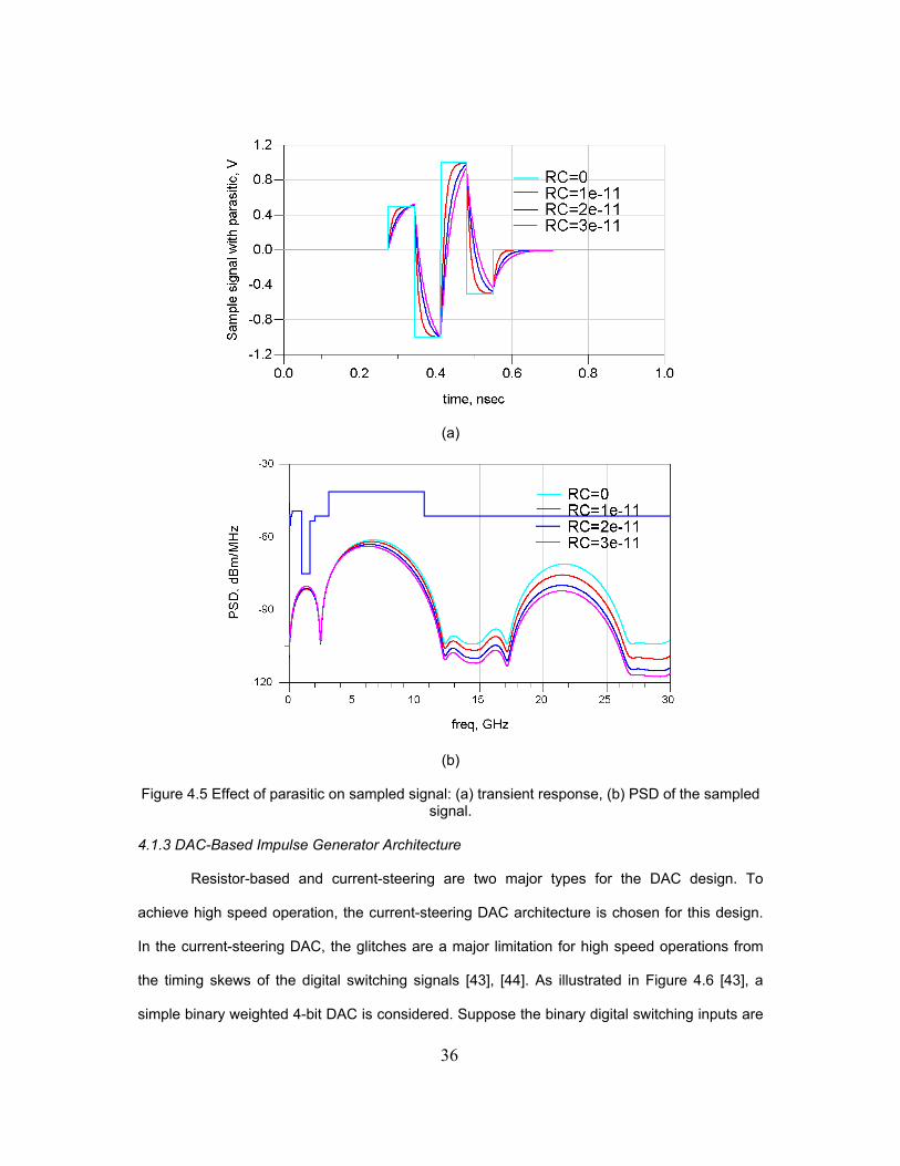
(a) peak sampling, (b) sampled signal, (c) PSD of the sampled signal. .................................. 35 4.5 Effect of parasitic on sampled signal:
(a) transient response, (b) PSD of the sampled signal. ........................................................... 36 4.6 Glitch in current-steering DAC: (a) transition from 1000 to 0001, (b) output glitch. ................. 37 4.7 Architecture of the proposed DAC impulse generator. ............................................................ 38 4.8 Timing diagram of pulse generation with sequence of switch inputs. ...................................... 39 4.9 Schematic of the proposed DAC impulse generator. ............................................................... 41 4.10 Equivalent small signal circuit of proposed DAC impulse generator. .................................... 42 4.11 Generation of digital switch control signals:
(a) digital circuit implementation, (b) timing diagrams. .......................................................... 44 4.12 Synchronization of switch control signals. ............................................................................. 45 4.13 OOK: (a) block diagram, (b) timing diagrams. ....................................................................... 46 4.14 The differential DAC impulse generator. ................................................................................ 47 4.15 Bi-phase operations with single-ended architecture. ............................................................. 48 4.16 Proposed digital BPM modulator. ........................................................................................... 49 4.17 Simulation of single-ended DAC impulse generator output with PRF of 50 MHz:
(a) transient response, (b) PSD. ............................................................................................ 50 4.18 Simulation of single-ended DAC impulse generator output with PRF of 100 MHz:
(a) transient response, (b) PSD. ............................................................................................ 51 4.19 Simulation of OOK output. ..................................................................................................... 52 4.20 Comparison of PSD at PRF of 50 MHz: (a) with OOK, (b) without OOK. .............................. 52

xii
4.21 Comparison of PSD at PRF of 100 MHz: (a) with OOK, (b) without OOK. ............................ 52 4.22 Simulation of differential DAC impulse generator:
(a) transient response, (b) PSD. ............................................................................................ 53 4.23 Simulation of bi-phase modulation output at PRF of 1 GHz. ................................................. 54 4.24 Comparison of PSD at PRF of 50 MHz:
(a) with BPM modulation, (b) without BPM modulation. ........................................................ 55 4.25 Comparison of PSD at PRF of 100 MHz:
(a) with BPM modulation, (b) without BPM modulation. ........................................................ 55 5.1 Architecture of the proposed UWB impulse generator. ............................................................ 57 5.2 (a) Gaussian pulse generator output spectrum, (b) BPF frequency
response, (c) BPF and antenna output spectrum. ................................................................... 58 5.3 BPF output PSD with different input Gaussian pulses. ............................................................ 61 5.4 CML inverter. ............................................................................................................................ 62 5.5 Pulse generations with XOR gate. ........................................................................................... 63 5.6 Static logic XOR gate: (a) circuit implementation, (b) RC equivalent circuit. ........................... 63 5.7 Compact XOR gate: (a) circuit implementation, (b) timing diagram. ....................................... 64 5.8 (a) Schematic of the proposed Gaussian pulse generator, (b) timing
diagram of the pulse generator out. ......................................................................................... 66 5.9 Transient and spectrum simulation results of the Gaussian pulse equation. ........................... 67 5.10 Propagation delay in the delay cell. ....................................................................................... 68 5.11 Schematic of the first-order Butterworth BPF. ....................................................................... 70 5.12 Schematic of RLC antenna model [48]. ................................................................................. 71 5.13 Gaussian pulse generator transient output. ........................................................................... 71 5.14 Impulse generator transient output. ....................................................................................... 72 5.15 Output PSD with PRF of 50 MHz. .......................................................................................... 72 5.16 Output PSD with PRF of 100 MHz. ........................................................................................ 73

xiii
5.17 Output PSD with PRF of 200 MHz. ........................................................................................ 73 5.18 OOK modulated output signals. ............................................................................................. 74 5.19 Comparison of PSD at PRF of 200 MHz: (a) with OOK, (b) without OOK. ............................ 74 5.20 PSD of the impulse generator output with 50-Ω load and with
RLC antenna model. .............................................................................................................. 75 5.21 Chip photo of the proposed impulse generator. ..................................................................... 76 5.22 Measurement setup................................................................................................................ 76 5.23 Measured transient response of the impulse generator......................................................... 77 5.24 Measured PSD of the impulse generator output:
(a) at 100 MHz PRF, (b) at 200 MHz PRF. ............................................................................ 78 6.1 Block diagram of the proposed carrier-based impulse generator. ........................................... 81 6.2 VCO and buffer. ....................................................................................................................... 83 6.3 VCO RLC model. ...................................................................................................................... 84 6.4 Negative resistance from the cross coupled NMOS pair. ........................................................ 84 6.5 Typical source follower with current source load. .................................................................... 86 6.6 RLC model of proposed VCO buffer. ....................................................................................... 87 6.7 Common switch types. ............................................................................................................. 89 6.8 Shunt switch simplified equivalent circuits. .............................................................................. 89 6.9 RF SPST switch. ...................................................................................................................... 90 6.10 Effect of gate biasing resistor. ................................................................................................ 91 6.11 Body floating technique [64]: (a) equivalent model of shunt
transistors in off-state, (b) without body resistor, (c) with body resistor. ................................ 92 6.12 Proposed pulse generator: (a) schematic, (b) timing diagram. .............................................. 94 6.13 Phase noise of VCO with buffer. ............................................................................................ 95 6.14 Insertion loss and isolation of RF shunt switch. ..................................................................... 95

xiv
6.15 Simulation of impulse generator. ............................................................................................ 96 6.16 Impulse generator output: (a) transient response, (b) PSD. .................................................. 97 6.17 Impulse generator output with varactor biased at -2.5 V:
(a) transient response, (b) PSD. ............................................................................................ 98 6.18 Impulse generator output with varactor biased at 2.5 V:
(a) transient response, (b) PSD. ............................................................................................ 99 6.19 Chip photo of the impulse generator. ................................................................................... 100 6.20 Measurement setup.............................................................................................................. 100 6.21 Measurement of transient impulse generator output. .......................................................... 101 6.22 Measurement of impulse generator output PSD. ................................................................. 102 6.23 Block diagram of the proposed transmitter. ......................................................................... 103 6.24 Schematic of the differential VCO with buffers. ................................................................... 103 6.25 Schematic of the cascaded RF SPST switches. .................................................................. 104 6.26 Schematic of the bi-phase modulator. .................................................................................. 106 6.27 Transient simulation of the transmitter. ................................................................................ 107 6.28 Comparison of the bi-phase transmitter outputs. ................................................................. 108 6.29 PSD of the transmitter out. ................................................................................................... 108
xv
LIST OF TABLES
Table Page 2.1 FCC emission limits .................................................................................................................... 8
4.1 Required switch input sequences ............................................................................................ 40
4.2 Truth table of the modulator ..................................................................................................... 49
5.1 Comparison table of existing CMOS filtering-type impulse generators ................................... 79

1
CHAPTER 1
INTRODUCTION
Ultra-wideband (UWB) technology has attracted a lot of academic and industrial
interests, since the United States Federal Communications Commission (FCC) classified the
using of UWB technologies in certain frequency bands in 2002 [1]. The UWB spectrum is
generally classified by: 0-960 MHz (Sub-GHz) band for ground penetrating radar systems
(GPRs), wall imaging systems, and through well imaging system, 3.1-10.6 GHz band for
communication systems and medical systems, 1.99-10.6 GHz band for wall imaging systems,
through-well imaging systems, and surveillance systems, and 22-29 GHz band for automotive
radar systems. Regardless of system classification, all of the bands have a -10 dB system
bandwidth within the band as well as an imposed average power spectral density restriction of -
41.3 dBm/MHz.
Among all the regulation bands, 3.1-10.6 GHz and 22-29 GHz bands have drawn most
of attentions because of the variety of the applications and direct benefits with UWB
implementations. They also provide the opportunity of system-on-chip realization using more
cost-effective CMOS technology. For current wireless communication applications, high data
rate, low power, and low cost are desirable because of the surging demand for enhanced
performance, battery-life, and cost efficiency of the electronic devices. The UWB technology
has been proven to satisfy the above requirements from its unique characteristics. As for the
automotive radar application, The 22-29 GHz radar is defined as the short range radar (SRR)
which can be operated with high range resolution and finds the applications such as anti-
collision sensing, adaptive cruise control (ACC) support, blind spot detection, and parking aid
[2], [3], which dramatically brings the convenience and increases the safety for drivers on the
hazardous roads.

2
Conventionally, for the UWB communication and radar systems, either carrier-based
UWB signals or carrier-free UWB signals are employed. Both architectures have advantages
and disadvantages over each other. The carrier-based UWB systems like pulse modulation,
spread spectrum, and orthogonal frequency division multiplexing (OFDM) require oscillators to
generate the wideband signal introducing the extra power consumption. Additionally, the pulse
modulation technique uses either RF switch or mixer to modulate the signal causing either
carrier-leaking from the finite isolation of the switch or larger power consumption from the mixer.
The spread spectrum technique uses pseudo-noise (PN) code generator modulating the signal
to achieve the wide bandwidth. However, the noise-like spread spectrum signal has a low
signal-to-noise ratio (SNR) and thus processing and extracting information become a challenge
for the receiver. In case of OFDM technology, the whole spectrum is divided into several sub-
bands having minimum bandwidth of 500 MHz. As different carrier frequencies are required for
different bands, system architecture becomes more complex. Despite the additional power
consumptions and complex architectures, the carrier-based UWB system has the advantages of
easy signal generations, more spectrum controllability, less passing antenna distortions, and
easing the design of all components because of the narrower bandwidth [4]. Meanwhile, the
carrier-free UWB directly generates very short-duration UWB impulses without using carrier
signals. Thus, carrier-free UWB systems can has lower power consumption and simpler
architectures comparing with carrier-based systems. However, the advantages of carrier-free
UWB are sometimes neutralized by certain disadvantages such as impulse signal generations,
critical synchronization requirements at the receiver end, and antenna distortions [5], [6].
Therefore, due to the trade-off between power consumptions and circuit realizations, designers
can choose either architecture depending on the application requirements.
Among all the UWB systems, impulse-radio UWB (IR-UWB), as opposed to continuous
wave UWB (CW-UWB), employs a pulsed-signal with very narrow pulse width producing a very
wide bandwidth in frequency, which can lower worst-case multipath fading, have an excellent

3
immunity to interference from other radio systems, and provide an enhanced range resolution
for the radar system. The IR-UWB is also the original concept of UWB from the definition by the
FCC [1].
For the IR-UWB system, many components have been developed and implemented
using CMOS or other Si-based processes, such as impulse generator [7]-[12], low-noise
amplifier [13]-[15], mixer [16]-[18], and power amplifier [19], [20]. Among all the components, the
impulse generator is a critical component generating the signal for the system to meet the FCC
emitting power regulation and to fully utilize the allocated spectrum, as the same copy of the
impulse generator will also be used in the receiver for signal acquisitions.
For the UWB communication systems, to date, several methods have been deployed
for IR-UWB pulse generation using CMOS technology such as the pulse-combination method
[7], [8], the digital-to-analog converter (DAC) method [9], and the filtering method [10]-[12]. The
pulse-combination method in [7], [8] employs more complex architectures of digital circuits to
realize the pulse generation requiring precise synchronization from the delay lines. For the DAC
method, the resistor-ladder DAC-based impulse generator shows high complexity owing to the
large number of the passive components [9]. The filtering method has been developed using
passive filters and active filters. The passive filter in [10] uses on-chip passive components such
as inductors and capacitors and occupies large chip area. Also, the off-chip passive filter is
implemented using a microstrip line, which is not fully integrated [11]. As an alternative filtering
method, the active FIR filter is employed for on-chip integration [12], but the design architecture
is complex and the power consumption is relatively high.
For the UWB automotive radar systems, the SiGe technology is mostly used since
there are still difficulties to overcome using CMOS technology. However, the more cost-effective
CMOS process can provide the opportunities of low cost and also low power characteristics into
the system. Up to date, only a few CMOS impulse generators have been proposed for UWB
SRR applications [21]-[23]. A Carrier-free impulse generator was proposed in [21]. However, the

4
transmitter in [21] has a complex architecture and requires critical device matching for delay
blocks to comply with the FCC regulation. For other UWB impulse generators in [22], [23], the
carrier-based architectures were presented. Because the designs use mixers and power
amplifiers, there will be additional power consumptions and less power efficiency.
In this dissertation, for UWB communication systems, the carrier-free IR-UWB impulse
generators based on the DAC and passive-filtering method are presented. The proposed DAC-
based impulse generator is designed using CMOS 0.18 μm technology employing a current-
steering architecture, which has the feature of high speed, high tuning-ability and simplex
architecture for the UWB communication systems. The passive-filtering impulse generator, fully
integrated in CMOS 90 nm process, consists of a novel pulse generator employing least
transistors among other existing designs with a compact on-chip band-pass filter providing low-
cost, low-power, and low-complexity for the UWB communication systems. For UWB
automotive radar systems, a carrier-based IR-UWB CMOS impulse generator using CMOS 130
nm process is proposed with a switch-based pulse modulation architecture generating a robust
UWB signals while achieving high power efficiency and high range resolution.
This dissertation is organized with seven chapters. In Chapter 2, the background of
UWB definition, FCC regulations, and UWB systems are discussed. Chapter 3 addresses the
existing architectures of the UWB impulse generator. Various modulation schemes in UWB
systems are also described. Chapter 4 presents the proposed UWB DAC-based impulse
generator with simulation results. The proposed filtering-type UWB impulse generator is
presented in Chapter 5 with simulation and measurement results. In Chapter 6, the carrier-
based impulse generator for UWB vehicular radar applications is presented with simulation and
measurement results. The final chapter summarizes and concludes the results of this research.

5
CHAPTER 2
BACKGROUND
In this chapter, the fundamentals of UWB technology are introduced. The history,
concept, and advantages of the UWB technology are presented. The UWB applications as well
as the emission regulations according to the FCC are examined showing the reasons that the
UWB technology is attractive and benefits the UWB technology can bring. Different UWB
systems and their architectures are also presented.
2.1 Brief History of Ultra-Wideband
The concept of UWB technologies is actually not new. UWB communications and radar
systems have been in existence for some time already, although they have not always been
referred to “Ultra-wideband”. Traditionally, UWB signals have been obtained by generating very
narrow pulses, rather than continuous waveforms (sinusoidal waves), with no radio frequency
(RF) modulation. This technique has been commonly used in radar applications as referred to
impulse radio (IR).
For wireless communication systems, unlike today’s dominant method of using
sinusoidal waves to transfer information, the technique was based on the emission of pulse-
based signals. Back in 1894-1896, Marconi carried out a spark-gap transmission experiment
which is considered as the first experiment of impulse radio. However, due to the technical
limitation and flavor for reliable communications, using continuous waveforms became the
major trend, and IR remained confined to the radar applications.
In 1973, the first patent was awarded to Ross for an UWB communication system, but
different nomenclature was used, and then the UWB field moved to a new direction. Through
the 1980’s, UWB technology was commonly referred to as carrier-free, base-band, or impulse
communication. It was not until 1989 that the term “Ultra-wideband” was coined by the United

6
States Department of Defense. The Department of Defense had been using the technology
since the early 1960’s, but much of the technological advances prior to 1994 were classified.
However, since the commercial market can benefit dramatically from UWB capable systems,
the Federal Communications Commission has passed legislation allowing the use of Ultra-
wideband systems. In the late 1990’s, the development of UWB systems was commercialized
by several companies such as Time Domain and Xtreme-Spectrum.
2.2 Definition of UWB Systems
According to the FCC report in 2002 [1], an UWB signal is defined to have a spectral
occupancy over 500 MHz or a fractional bandwidth of more than 20 %. Fractional bandwidth, as
defined by the FCC, is given by
(2.1)
where fU and fL are the upper and lower -10 dB emission points, respectively and fC is defined
as the center between fU and fL, as illustrated in Figure 2.1. The FCC specifies that a system
with center frequency in excess of 2.5 GHz must have a bandwidth of at least 500 MHz, but a
system whose center frequency is less than 2.5 GHz, must operate with a Fbw of at least 20 %
in order to be characterized as an UWB system. Comparing with narrowband (NB) signals,
UWB signals have a much wider bandwidth in frequency, which refers to a much narrower pulse
width in time domain with a pulse-based signal.
2)( )(
LU
LU
C
LUbw ff
fff
ffFrequencyCenter
BWBandwidthF+−
=−
==

7
fC fUfL
NB
UWB
f (Hz)
Pow
er S
pect
ral D
ensi
ty
-10 dB
Figure 2.1 UWB definitions.
2.3 UWB Regulations
In the April 2002, the Federal Communications Commission (FCC) established several
unlicensed bands and restricted transmitted power levels within those bands to be below the
noise floor, specifically below -41.3 dBm/MHz, thereby allowing for the possibility of commercial
UWB systems. Since UWB systems cover a large spectrum, the low output power restriction on
UWB systems ensures friendly coexistence with already available wireless systems with
tolerable mutual interference.
Table 2.1 summarizes the emission limits regulated by the FCC for the applicable UWB
applications. To the interests for this dissertation, the spectral mask transmission limits are
graphically depicted in Figure 2.2 and Figure 2.3, for UWB indoor/outdoor communication
systems operating in 3.1-10.6 GHz and UWB automotive radar applications operating in 22-29
GHz, respectively. EIRP stands for Equivalent Isotropically Radiated Power. The transmission
limit for the outdoor application is 10 dB lower from 1.61-3.1 GHz and the frequency above 10.6
GHz than the limit for indoor application to ensure better protection from harmful interference to
the U.S. Government operations within these bands as well as the operation of Digital Audio
Radio Service (DARS) and other communications systems operating within these bands under
outdoor environment. Regardless the different applications, all the regulated UWB bands have
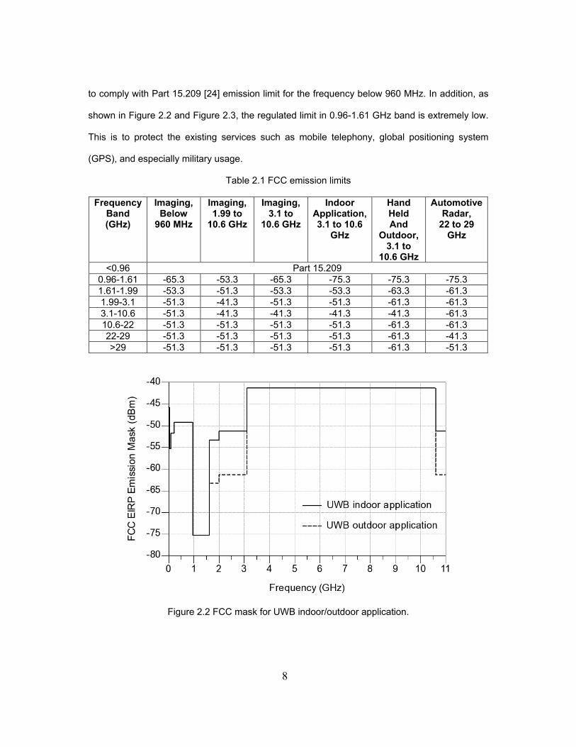
8
to comply with Part 15.209 [24] emission limit for the frequency below 960 MHz. In addition, as
shown in Figure 2.2 and Figure 2.3, the regulated limit in 0.96-1.61 GHz band is extremely low.
This is to protect the existing services such as mobile telephony, global positioning system
(GPS), and especially military usage.
Table 2.1 FCC emission limits
Frequency Band (GHz)
Imaging, Below
960 MHz
Imaging, 1.99 to
10.6 GHz
Imaging, 3.1 to
10.6 GHz
Indoor Application, 3.1 to 10.6
GHz
Hand Held And
Outdoor, 3.1 to
10.6 GHz
Automotive Radar,
22 to 29 GHz
<0.96 Part 15.209 0.96-1.61 -65.3 -53.3 -65.3 -75.3 -75.3 -75.3 1.61-1.99 -53.3 -51.3 -53.3 -53.3 -63.3 -61.3 1.99-3.1 -51.3 -41.3 -51.3 -51.3 -61.3 -61.3 3.1-10.6 -51.3 -41.3 -41.3 -41.3 -41.3 -61.3 10.6-22 -51.3 -51.3 -51.3 -51.3 -61.3 -61.3 22-29 -51.3 -51.3 -51.3 -51.3 -61.3 -41.3 >29 -51.3 -51.3 -51.3 -51.3 -61.3 -51.3
Figure 2.2 FCC mask for UWB indoor/outdoor application.

9
Figure 2.3 FCC mask for UWB automotive radar application.
2.4 UWB Properties
The distinct properties of UWB signals can provide various advantages to different
applications. For wireless communication systems, UWB signals have the capability to convey
the data with very high-speed. The qualities of UWB systems can be illustrated by Shannon’s
Information Capacity theorem. Shannon’s theorem states that maximum theoretical channel
capacity (C in bits per second) is a function of channel bandwidth (B), signal power(S), and
noise power (N) and is given by [25]
)1(log2 NSBC +⋅= (2.2)
In case of narrow band systems, bandwidth of channel is limited thus in order to
increase data rate, only choice is to increase signal power. While in UWB communication
systems, since available bandwidth is huge, the large data rates can be achieved with less
signal power transmitted. UWB communication systems are also inherently secure. Since the
maximum allowable emission spectrum of UWB signal is normally below environment noise,
only the receiver that acknowledges the action of transmitter can decode the receiving random
10
pulses. Other narrowband receivers may not even distinguish the difference between UWB
signals and the environment noise. This property of UWB is desirable in highly secure
communication systems, such as in military walkie-talkie systems.
For IR-UWB systems, the low-power and low-cost advantages stem from the
essentially baseband nature of the signal transmission. Comparing to conventional transceiver,
the IR-UWB transceiver has the simpler architecture with fewer components. At the receiver
end, there is no need of local oscillators generating the carriers and as the matched filter is
employed, the analog-to-digital converter (ADC) can operate at bit rate. On the other hand, the
transmitter needs no DAC and additional RF mixing stage generating the short duration signals
directly to the antenna without amplification.
As for the advantages of UWB signals mentioned above, there are also disadvantages
as follows. Although IR-UWB can have a simpler architecture, due to the narrow transmitting
pulses, the synchronization of matched filter in the receiver become critical. The antenna design
for the UWB systems become challenging to achieve wideband, compact, and low-cost. The
range of the UWB system is also limited especially for communication operating in higher data
rate owing to the low emission limits constrained by the FCC.
Since the IR-UWB pulses have very short pulse width, UWB radio systems are
potentially able to offer precision timing and fine range resolution much better than GPS and
other radio systems. And since the IR-UWB pulses are shorter than the target dimensions, the
UWB signals have remarkable sensitivity to scattering and good material penetrating comparing
to narrowband signals.
2.5 UWB Applications
UWB applications to wireless communications and radars are most widely appreciated.
For UWB wireless communications, the advantages of UWB systems are available in short
range applications. Since it achieves very low power at relatively low cost, UWB communication
systems are very advantageous in short-range wireless market. UWB technologies are primarily
11
targeting at indoor wireless communication applications around 10 meters at bit rates up to
hundreds of megabits per second, such as high-quality real-time video and audio distribution,
file exchange among storage systems, and cable replacement for home entertainment.
For the radar applications, the imaging systems and vehicular radar systems can be
enhanced by adopting UWB signals. Imaging systems include GPRs, wall imaging systems,
through-wall imaging systems, surveillance systems and medical systems, which can be
benefited since UWB waveforms exhibit pronounced sensitivity to scattering relative to
conventional radar signals. As for short-range vehicular radar system, using UWB signals
provides vary benefits since in UWB systems, pulses with very short duration are sent greatly
improving the radar range resolution as well as reducing the multipath fading.
2.6 UWB System Architectures
There are mainly two types of system architectures which can be employed to efficiently
use the regulated UWB spectrum. They are namely impulse type UWB (IR-UWB) and carrier-
based UWB (OFDM, spread spectrum). Both system architectures have certain advantages and
disadvantages over each other. Especially, the OFDM system and IR-UWB system were the
two major competing proposals for IEEE 802.15.3a standards. However, after several years of
deadlock, the IEEE 802.15.3a task group was dissolved in 2006. WiMedia Alliance supports a
type of OFDM architecture referred to as multiband OFDM (MB-OFDM) while the UWB forum
was proposing a form of IR-UWB called Direct Sequence UWB (DS-UWB). However, UWB
forum is now defunct after the majority members Motorola and Freescale left the grounp in
2006. Nonetheless, it is already decided that for 802.15.4 standard, IR-UWB is to be included
because of its low-power, simplicity, and localization capabilities.
2.6.1 IR-UWB System
In IR-UWB systems, pulses with very short duration (typically few nanoseconds) are
transmitted without using oscillator. The transmitted signals should comply with the FCC EIRP
mask with certain pulse repetition frequency.

12
There are basically two different types of receivers employed in IR-UWB systems,
namely coherent receiver and non-coherent receivers. Figure 2.4 shows the typical IR-UWB
coherent receiver. The analog correlator consisting of mixer, integrator, and dump correlates the
input RF signal to locally generated UWB impulses from template generator. The output of the
receiver is maximized when template and input RF signals are synchronized in time. Thus, if
template and input RF signal are not aliened then output cannot have all the energy from input
RF signal. The correlator provides the functionality of an optimum matched filter which
maximizes the signal-to-noise ratio (SNR). Since integrator and dump work as a low-pass filter,
the baseband output signal can be easily sampled by the ADC, relaxing the requirement on
sampling rate and reducing the possible excessive power consumption. However, as mentioned
before, due to the very narrow pulse signals, generating the precise timing control and fine step
template signals becomes critical, and synchronization takes longer time. Thus, it is sometimes
necessary to use serial search correlators to reduce the acquisition time.
Figure 2.4 The coherent IR-UWB receiver.
Figure 2.5 shows the non-coherent type receiver. In this type of receiver, input RF
signal self-correlated by one period delayed signal. The correlation operation reveals the
amplitude variations from one pulse to the other, carrying the transmitted information. Thus,
before each data signals, the transmitter should also send the reference pulses. This increases
the overhead as far as transmitter is concerned and increases the power requirements. Since
the adaptive noise in the receiver, the delay cell used to delay the reference pulses becomes
critical.

13
Figure 2.5 The non-coherent IR-UWB receiver.
In practical wireless communications, the channel suffers from multipath effect, where
reflections of the transmitted signals and other effects of the channel cause multiple copies of
the original transmitted pulse appearing at the receiver end. Therefore, a rake receiver is
usually used to improve reception at the cost of increased receiver complexity. The increased
complexity comes from the multi fingers of correlators required to estimate and track multiple
impulses while demodulating them.
2.6.2 Carrier-Based UWB System
In the carrier-based UWB system, oscillators are normally employed as the template for
correlation with the receiver input signal. Figure 2.6 shows the typical architecture of carrier-
based system. It contains two channels namely I and Q channels. Template signals are usually
continuous wave signals from local oscillators. I channel uses sine wave as a template signal
while Q channel uses 90o phase shifted sine wave (cosine wave) as a template. By using both I
and Q channels with 90o phase shifted template signals, the system can recover and obtain the
information of the received signal (magnitude and phase). Low pass filter is used to recover the
baseband signal. This type of receiver is traditionally called as ‘Envelope Detector’. This
approach gives less SNR value than the matched filter type receiver. And since the architecture
is more complex than that of the IR-UWB, more power is consumed from the excessive
components especially oscillators.
14
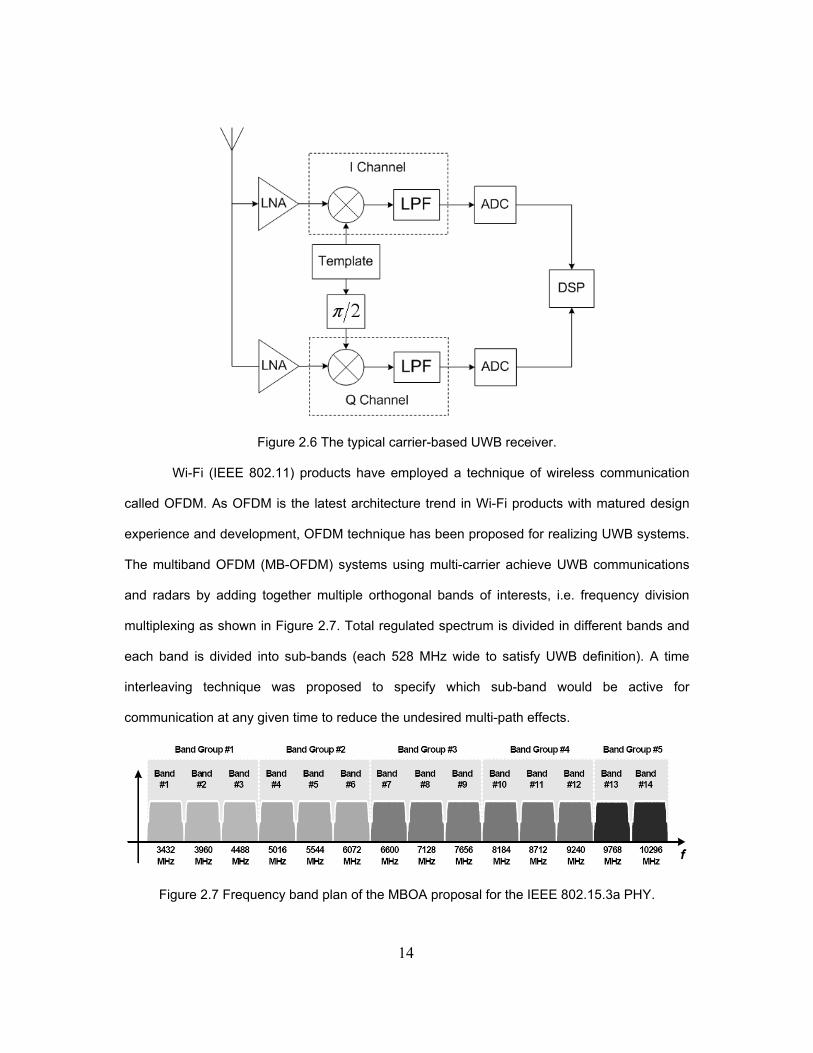
Figure 2.6 The typical carrier-based UWB receiver.
Wi-Fi (IEEE 802.11) products have employed a technique of wireless communication
called OFDM. As OFDM is the latest architecture trend in Wi-Fi products with matured design
experience and development, OFDM technique has been proposed for realizing UWB systems.
The multiband OFDM (MB-OFDM) systems using multi-carrier achieve UWB communications
and radars by adding together multiple orthogonal bands of interests, i.e. frequency division
multiplexing as shown in Figure 2.7. Total regulated spectrum is divided in different bands and
each band is divided into sub-bands (each 528 MHz wide to satisfy UWB definition). A time
interleaving technique was proposed to specify which sub-band would be active for
communication at any given time to reduce the undesired multi-path effects.
Figure 2.7 Frequency band plan of the MBOA proposal for the IEEE 802.15.3a PHY.

15
The PHY (physical) layer of proposed MB-OFDM is basically a descendant from 802.11
a/g systems. These systems have potential of achieving high data rates from the more utilized
frequency bands. However, like other carrier-based system, MB-OFDM suffers high power
consumption and high circuit complexity. Figure 2.8 shows the block diagram of the typical MB-
OFDM receiver proposed for IEEE 802.15.3a PH layer by the Multiband Alliance (MBOA). From
the figure it is evident that this architecture is much more complicated and consumes more
power compared to IR-UWB systems. This is the reason that this system architecture is not
chosen for IEEE 802.15.4 standard.
Figure 2.8 The typical UWB MB-OFDM receiver.

16
CHAPTER 3
OVERVIEW OF UWB IMPULSE GENERATOR
In UWB systems, impulse generator plays an important role to generate the transmitting
signals complying with the FCC regulations. The transmitting signals should sufficiently utilize
the designated UWB spectrum. Once the transmitting signal is generated, the design
specifications and requirements (speed, bandwidth, etc.) for the receiver components can be
also determined. Also, the impulse generator may be used as the template generator in the
receiver. Generally, for the UWB signal generation, there are two approaches: temporal or
frequential. Temporal approach, like IR-UWB, attempts to generate wideband signals with very
short duration in time directly from the baseband signal (Gaussian pulses). On the other hand,
frequential approach accomplishes the wide bandwidth directly from frequency domain using
techniques like up-converting or spectrum spreading. In the following subsections, several
existing architectures of the UWB impulse generator will be introduced and the applicable
modulation schemes and their characteristics for the IR-UWB impulse generator are also
discussed.
3.1 Carrier-Free IR-UWB Impulse Generator
3.1.1 IR-UWB Waveforms
As mentioned, since IR-UWB achieves wide bandwidth from time domain employing
short duration pulses, one of the most important design considerations is the selection of the
fundamental pulse shape. The Gaussian pulse, often referring to a monocycle, has been
theoretically proven to be a good fundamental baseband pulse for IR-UWB system [26]-[28].
The general Gaussian pulse is given by
)2
exp(2
)( 2
2
σσπtAtx −= (3.1)
17
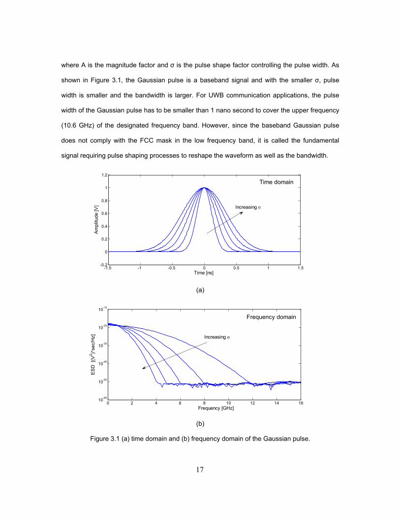
where A is the magnitude factor and σ is the pulse shape factor controlling the pulse width. As
shown in Figure 3.1, the Gaussian pulse is a baseband signal and with the smaller σ, pulse
width is smaller and the bandwidth is larger. For UWB communication applications, the pulse
width of the Gaussian pulse has to be smaller than 1 nano second to cover the upper frequency
(10.6 GHz) of the designated frequency band. However, since the baseband Gaussian pulse
does not comply with the FCC mask in the low frequency band, it is called the fundamental
signal requiring pulse shaping processes to reshape the waveform as well as the bandwidth.
-1.5 -1 -0.5 0 0.5 1 1.5-0.2
0
0.2
0.4
0.6
0.8
1
1.2
Time domain
Time [ns]
Am
plitu
de [V
] Increasing σIncreasing σIncreasing σIncreasing σIncreasing σ
(a)
0 2 4 6 8 10 12 14 1610-60
10-50
10-40
10-30
10-20
10-10
Frequency domain
Frequency [GHz]
ES
D [
(V2 )*
sec/
Hz] Increasing σIncreasing σIncreasing σIncreasing σIncreasing σ
(b)
Figure 3.1 (a) time domain and (b) frequency domain of the Gaussian pulse.

18
To shape the Gaussian pulse, several techniques have been developed (filtering
method, pulse combination method, etc.). As for the waveform of the reshaped UWB signals
complying with FCC regulations, the higher-order derivatives of the Gaussian pulse have been
analytically proven to sufficiently satisfy the spectrum and power requirements [27]. The n-th
derivative of Gaussian pulse can be determined as
)()(1)( )1(2
)2(2
)( txttxntx nnn −− −−
−=σσ
(3.2)
While the power spectral density (PSD) of the signals is given [20] by
)exp()2(exp)2()()(
22max
max nnffAfPAfP n
n
nt −−
==σπσπ
(3.3)
where Amax is the peak PSD the FCC permits and )( fPn is the normalized PSD. Thus, the
selection of parameters n and σ can determine the pulse shape as well as the PSD to comply
with the FCC mask. The PSD peak frequency, fpeak, can be related to n and σ with the
relationship given [27] by
πσ21nf peak = (3.4)
As can be seen, the higher order of Gaussian derivatives can result in a higher peak
frequency. Thus, through the differentiation, the energy can be moved to higher frequency
bands because of more zero crossings in the same duration of time. In [27], the 5-th order of
Gaussian derivatives is demonstrated to best satisfy the FCC mask for indoor UWB systems.
The PSD of different Gaussian derivatives (first to fifth order) with the FCC mask is shown in
Figure 3.2. With the same pulse shape factor σ, the higher the order is, the smaller the
bandwidth will be with the increasing of the peak frequency.

19
Figure 3.2 PSD of first to fifth order of Gaussian pulse.
3.1.2 Filtering-Based Impulse Generator
Figure 3.3 shows the typical filtering based impulse generator. The Gaussian pulse
generator usually consists of digital logic circuits generating the short-duration Gaussian pulses,
which requires a clock signal as the input that determines the output pulse repetition frequency.
As mentioned before, the generated Gaussian pulse width has to be narrow enough to cover
the desired frequency band. Then, the filter, also called pulse shaper, can be applied to remove
the unwanted spectrum especially in the low frequency band. For the type of filters, either
passive filters or active filters can be employed. The passive high-pass or band-pass filter can
be used as passive filter, while the finite impulse response (FIR) filter consisting of transistors
can be used as active filter.

20
Figure 3.3 Architecture of the typical filtering based impulse generator.
Figure 3.4 shows the example of filter based impulse generator proposed in [10]. The
baseband generator consists of digital delay cell and logic gate combining the edges of the
input signal to produce the Gaussian-like waveform. The on chip filter is implemented as a third
order passive Bessel band-pass filter constructed by three inductors and four capacitors. All the
circuits are implemented using CMOS technology allowing low cost and low power. However,
the large number of passive components occupies more chip area.
Figure 3.4 Architecture of the passive filtering impulse generator [10].
To reduce the using of passive components and the chip area, the active FIR filter can
be used as the pulse shaper as presented in [12]. Instead of the baseband pulse, the rising and
falling edges of the digital clock signal are directly employed as the input of the FIR filter to
generate the derivatives of the Gaussian pulse. The block diagram of the FIR filter impulse
generator is shown in Figure 3.5. The architecture consists of the digital delay line and taps of
FIR filter. The output UWB signal is obtained by adding time-shifted and scaled versions of the
clock edge. However, except FIR filter, extra circuitries are needed to generate the control

21
signals for the filter and a wideband balun is needed to convert the differential filter output to
single-ended signal. As a result, the design has a complex architecture and power consumption
is relatively high.
Figure 3.5 Block diagram of the FIR filtering impulse generator [12].
3.1.3 DAC-Based Impulse Generator
The digital-to-analog converter (DAC) has also been adopted as the method to convert
digital input data to analog UWB signals. In [9], resistive ladder based DAC is used as shown in
Figure 3.6. The resistor ladder divides the voltage source Vdd into different levels and the
combination of switches are controlled by pairs of digital input signal. By turning on and off the
switches in a particular sequence, the desired output impulse pattern can be formed. However,
the passive resistors employed increase the chip area and require device matching to ensure
evenly distributed output levels.

22
Figure 3.6 Block diagram of the resistor ladder DAC impulse generator [9].
On the other hand, the current-steering DAC is employed to reduce the using of
passive components [29], [30]. The architecture of the current-steering DAC impulse generator
is shown in Figure 3.7, which consists of load resistors and several current cells. By controlling
the timing of each switch in the current cell, the different output currents can be formed from
combinations of current drawn in each cell and thus the desired output waveform is generated.
However, these DAC-based impulse generators require on chip memory enlarging chip areas.
Moreover, these designs are implemented using BiCMOS technology. In spite of the types of
DAC employed, this method usually requires additional circuits to generate the switch control
signals raising the complexity of the circuit as well as the power consumption. The method also
requires high speed (high sampling rate) from the switching, which is a challenge for designing
the circuit.

23
Vdd
MSBLSB
VoutVout
Figure 3.7 Block diagram of the current steering DAC impulse generator [29], [30].
3.1.4 Pulse Combination Type Impulse Generator
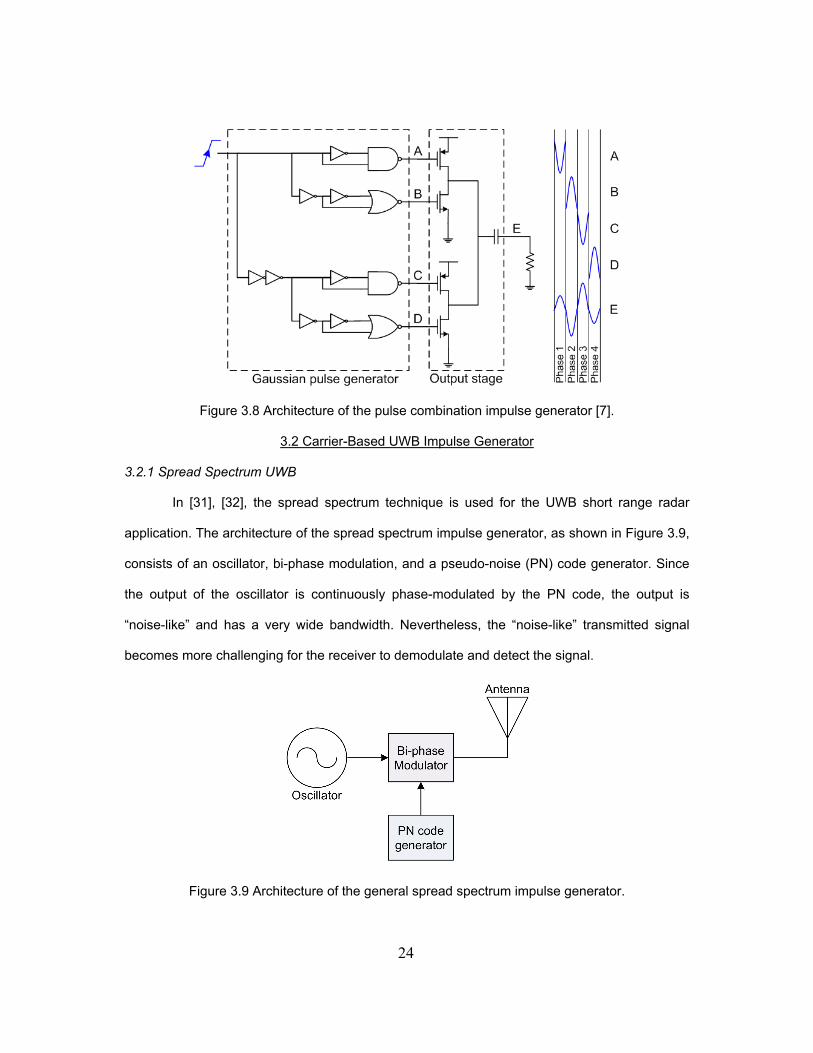
As shown in Figure 3.8, an impulse generator proposed in [7] is composed of Gaussian
pulse generators and combining output stage. The Gaussian pulse generators are digital
circuits producing Gaussian-like pulses (A, B, C, and D) in different phase and polar from
different delay and logics. The output stage containing two digital invertors then transforms the
variations of input pulses to single voltage output with combined waveform. The combined
output is an approximate 5-th order Gaussian derivative which can meet the FCC mask for
UWB indoor application. Using this method can produce the high order Gaussian derivative
directly from baseband pulses without employing any filtering process. However, it requires
more complex digital circuitries and needs the accurate synchronization from each of the delay
cells to correctly combine the pulses in phase.
24
Figure 3.8 Architecture of the pulse combination impulse generator [7].
3.2 Carrier-Based UWB Impulse Generator
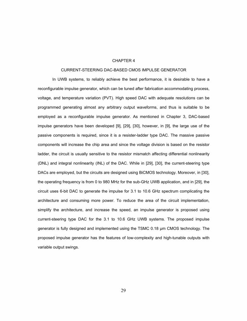
3.2.1 Spread Spectrum UWB
In [31], [32], the spread spectrum technique is used for the UWB short range radar
application. The architecture of the spread spectrum impulse generator, as shown in Figure 3.9,
consists of an oscillator, bi-phase modulation, and a pseudo-noise (PN) code generator. Since
the output of the oscillator is continuously phase-modulated by the PN code, the output is
“noise-like” and has a very wide bandwidth. Nevertheless, the “noise-like” transmitted signal
becomes more challenging for the receiver to demodulate and detect the signal.
Figure 3.9 Architecture of the general spread spectrum impulse generator.

25
3.2.2 Pulse Modulated UWB
Pulse modulated impulse generator, a carrier-based IR-UWB architecture, generates
short duration signals by modulating the carrier signal. In the pulse modulated signal
generation, there are mainly two methods employed; one is the mixer-based up-converting
method [33], the other is the switch-based on-off keying method [34]. The architecture of two
methods is shown in Figure 2.18. Both methods need a baseband pulse generator to modulate
the output of oscillator. At millimeter-wave frequencies, switch-based technique is more power
efficient [35] since the mixer, power amplifier, and other components in the mixer-based
technique are always “on” with a very low duty-cycle transmitting signal. However, one
drawback of the switch-based technique is the residual carrier leak owing to the limited isolation
from the RF switch [36].
(a) (b)
Figure 3.10 Architectures of pulse modulated impulse generator: (a) switch-based, (b) mixer-based.
3.3 IR-UWB Modulation
3.3.1 Modulation Methods
Since single UWB impulse does not contain information itself, the digital information
can be added by means of modulation. There are several modulation methods for UWB system
as shown in Figure 3.11. The methods can be categorized as time-based technique, like pulse
position modulation (PPM) and shape-based technique including bi-phase modulation (BPM),
on-off keying (OOK), and pulse amplitude modulation (PAM) [37].

26
1 0 0 1Data
(a)
(b)
(c)
(d)
Figure 3.11 Applicable UWB modulation methods: (a) PPM, (b) BPM, (c) OOK, (d) PAM.
The PPM has been the most common method. In the PPM, as depicted in Figure 3.11
(a), information is carried by whether delaying the un-modulated signal or not regarding to the
binary bit. Also this delay function can be described in the way that sent UWB pulse in advance
of a time. Therefore, the binary information can be delivered with a forward or backward shift in
time. Moreover, by specifying the time delay for each impulse, an M-ary system can be set.
However, for the UWB systems, since impulse is very narrow, the ultra fine time control of the
delay is needed for accuracy.
BPM is another commonly used method. As shown in Figure 3.11 (b), the signal is
modulated by inverting its phase when data is “0”. The advantage of using BPM is that the
mean of its pulse weight is 0, which can help diminishing the spectral spikes of the output PSD
without the need of dithering signals as in PPM [38], [39].

27
In Figure 3.11 (c), OOK modulates data with the presence of an impulse representing
“1” and absence representing “0”. The advantage of OOK is raised from its simplicity, but the
main disadvantage comes from the multipath. That is, it may become difficult to determine the
absence of the signal (“0”) from echoes of other signals. In Figure 3.11 (d), an example of pulse
amplitude modulation is given where a pulse with larger amplitude represents “1” and smaller
amplitude represents “0”. Generally, the PAM method representing logic ‘0’ with smaller
amplitude is not preferable to most short-range communications because the smaller amplitude
is more susceptible to noise interference than the larger amplitude as its counterpart.
3.3.2 Modulations and Output PSD
To understand the effect of modulations on the output spectrum, for example, as the
output impulse g(t) is linearly modulated by OOK or BPM, the sequence of the modulated
impulses can be expressed by the autocorrelation function as
∑∞
−∞=
⋅−⋅=k
Pk Tktgats )()( (3.5)
where Tp is pulse repetition interval and the sequence ak represents the information symbol. In
the case of OOK, ak is either 1 or 0. The PSD of the output sequence can be therefore found
from the Fourier transform of the autocorrelation function and is given by [40]
∑∞
−∞=
−+=j ppp
a
p
a
Tjf
TjG
TfG
TfPSD )()()()(
2
2
22
2
δµσ (3.6)
where G(f) is the Fourier transform of g(t); aµ and 2aσ are mean and variance of the sequence
data ak, respectively. The first term on the right hand side of equation 3.6 is the continuous
spectrum given in V2/Hz depending only on the spectral characteristic of g(t). The second term
presents a discrete spectrum given in V2 spaced apart by 1/Tp in frequency, which also refers as
spectral lines or spectral spikes. The magnitude of the discrete spectrum is proportional to
|G(f)|2 evaluated at f=j/Tp. Therefore, for a given bandwidth resolution (RBW) for measuring the

28
PSD, the ratio β of magnitudes between spectral lines and continuous spectrum at f=j/Tp can be
given as
RBWTpa
a
⋅⋅= 2
2
σµβ (3.7)
As PRF increases, Tp decreases, and β increases, which means that the magnitude of spectral
lines is higher than that of the continious spectrum at high PRF operations. This result limits the
capacity of the impulse generator to employ large-magnitude output signals since to meet the
FCC emmision regulation with higher PRF, |G(f)|2 has to be smaller, which is to reduce the
magnitude of output impulses. However, by applying modulations, as for OOK, aµ =0.5 and
2aσ =0.25, and for BPM, aµ =0 and 2
aσ =1, the ratio β is smaller than that without applying
modulations. This means the apearance of spectral lines can be recuced and thus the trade-off
between PRF and output magnitude can be suppressed though modulations.
29
CHAPTER 4
CURRENT-STEERING DAC-BASED CMOS IMPULSE GENERATOR
In UWB systems, to reliably achieve the best performance, it is desirable to have a
reconfigurable impulse generator, which can be tuned after fabrication accommodating process,
voltage, and temperature variation (PVT). High speed DAC with adequate resolutions can be
programmed generating almost any arbitrary output waveforms, and thus is suitable to be
employed as a reconfigurable impulse generator. As mentioned in Chapter 3, DAC-based
impulse generators have been developed [9], [29], [30], however, in [9], the large use of the
passive components is required, since it is a resister-ladder type DAC. The massive passive
components will increase the chip area and since the voltage division is based on the resistor
ladder, the circuit is usually sensitive to the resistor mismatch affecting differential nonlinearity
(DNL) and integral nonlinearity (INL) of the DAC. While in [29], [30], the current-steering type
DACs are employed, but the circuits are designed using BiCMOS technology. Moreover, in [30],
the operating frequency is from 0 to 980 MHz for the sub-GHz UWB application, and in [29], the
circuit uses 6-bit DAC to generate the impulse for 3.1 to 10.6 GHz spectrum complicating the
architecture and consuming more power. To reduce the area of the circuit implementation,
simplify the architecture, and increase the speed, an impulse generator is proposed using
current-steering type DAC for the 3.1 to 10.6 GHz UWB systems. The proposed impulse
generator is fully designed and implemented using the TSMC 0.18 μm CMOS technology. The
proposed impulse generator has the features of low-complexity and high-tunable outputs with
variable output swings.

30
4.1 Design of Proposed UWB Impulse Generator
4.1.1 Choice of Impulse Shape
For the UWB communication systems, various kinds of the transmitted signals can
potentially be used, such as Gaussian pulse, Gaussian monocycle, and Scholtz monocycle [41].
The main reason for choosing the pulse shape is to make the PSD of the generated pulse
meeting the FCC mask more efficiently, which allows the transmitted signal to carry more power
within the regulated bandwidth. The derivatives of the Gaussian pulse have been examined to
have the above feature. Specifically, in [27], the 5th-order derivative of Gaussian pulse is
analyzed and is proven to have the highest bandwidth occupation for UWB indoor
communication system from 3.1 GHZ to 10.6 GHz. The 5th-order derivative of Gaussian pulse
can be expressed as
)2
exp()215
210
2()(5_ 2
2
79
3
11
5
σσπσπσπttttAtG th −⋅+−⋅= (4.1)
where A is the magnitude index of the pulse and σ is the shape index that determines the pulse
width. By plotting equation 4.1 and simulating its PSD in Matlab, as shown in Figure 4.1, it can
be seen that the 5th-order derivative of Gaussian pulse has five finite roots and two roots at
infinity and the PSD of the pulse meets the FCC mask very efficiently. For the proposed impulse
generator, the revised 5th-order derivative of Gaussian pulse is used by removing both of the
small end lobes of the pulse. The reason to modify the pulse is to simplify the pulse generation
and thus the architecture of the circuits while still meeting the FCC mask sufficiently. The
modified pulse can be expressed as
)()(5_)(_5_ tRecttGtrivisedG thth ⋅= (4.2)
where Rect(t) represents a rectangular pulse function as
≤
=therwiseo t orf
tRect0
2/1)(
τ (4.3)
31
to exam the usage of modified Gaussian pulse, as shown in Figure 4.2, the transient response
and the frequency response of the ideal 5th-order derivative of Gaussian pulse and the its
modified pulse are compared. As can be seen, the modified Gaussian pulse is truncated from
the ideal one by removing the two ending lobes. Comparing with the PSD of the ideal Gaussian
pulse, the PSD of the modified pulse has a slightly smaller bandwidth and has a side-lobe in the
low frequency region. The side-lobe in the low frequency is formed from the sinc function. From
equation 4.2, since modified Gaussian pulse contains a rectangular function in time domain, it
transforms to the sinc function and convolutes with the frequency response of the ideal 5th-order
derivative of Gaussian pulse. Thus, it is proven that the truncated 5th-order derivative of
Gaussian pulse can be approximately employed as an ideal 5th-order derivative of Gaussian
pulse for the transmitting signal for the 3.1 to 10.6 GHz UWB systems.
(a)
(b)
Figure 4.1 (a) 5th-order derivative of Gaussian pulse, (b) PSD of the signal.

32
(a)
(b)
Figure 4.2 Comparison of transient response and PSD: (a) ideal 5th-order derivative of Gaussian pulse, (b) modified 5th-order derivative of Gaussian pulse.
4.1.2 DAC Impulse Generating Principle
The DAC-based impulse generator usually requires Nyquist rate sampling to
reconstruct the signal for the designated spectrum. However, since the designated spectrum is
from 3.1 to 10.6 GHz for the UWB application, it requires a sampling rate over 20 Gs/s. This
high sampling rate gives a challenging task for DAC design itself, as well as for generating the
high speed input data streams. This is why several existing DAC-based impulse generators are
designed using more costly high speed SiGe BiCMOS technology [29], [30], and using high
speed digital logic circuits such as current-mode logic, consuming higher power.
To alleviate the required sampling rate, a technique called peak sampling [42] can be
adopted. As seen from Figure 4.2, the proposed modified 5th-order derivative of Gaussian pulse
has the band-pass spectrum from its alternating peak and zero-crossing points in the transient

33
waveform. Thus, the sampling rate can possibly be reduced by sampling only peak points. That
is, as demonstrated in [42], the Nyquist rate sampling of 20 Gs/s is employed to generate UWB
signal covering 3 to 10 GHz band as in Figure 4.3 (a), while the sampling rate is reduced to half
at 10 Gs/s when sampling only at the peak points without the need of sampling at zero point as
in Figure 4.3 (b). By comparing the PSD of these two sampled signals, as shown in Figure 4.3
(c), there is only slight difference especially for the -10 dB bandwidth within the preferable UWB
spectrum. Thus, the peak sampling is an effective way to reduce required sampling rate and is
adopted in the proposed UWB DAC-based impulse generator simplifying the circuit architecture
and reducing the power consumption.
Figure 4.3 Comparison of UWB signal generation using different sampling rate [42]: (a) Nyquist sampling, (b) peak sampling, (c) PSD of the two sampled signals.
Therefore, the modified 5th-order derivative of Gaussian pulse adopted in our proposed
impulse generator can be peak sampled as shown in Figure 4.4 (a). The peak sampling rate in

34
this case is about 14 Gs/s. The normalized sampled signal waveform is generated using Matlab
codes as shown in Figure 4.4 (b) and is expressed as
+≤≤+−+≤≤++≤≤+−+≤≤
=
SS
SS
SS
S
th
ttt for ttt for ttt for
ttt for
tsampledG
τττττττ
435.032121
5.0
)(_5_
11
11
11
11
(4.4)
where Sτ is the sampling period. The PSD of the sampled signal, as shown in Figure 4.4 (c),
sufficiently meets the regulated UWB spectrum. Again, the side-lobe at the low frequency region
is from the sinc function and the harmonic peak spectrum at high frequency band is the imaging
component of the sampling product. Practically, the parasitic in the actual circuit will introduce
the low-pass filtering effect from the RC time constant increasing the rising and falling time of
the sampled signal. Thus, it is important to know the parasitic effect on the output waveform and
its PSD in advance, which confines the DAC circuit performance. To exam the parasitic effect,
the RC time constant is first obtained by assuming a first-order system and the impulse
response of the system can be therefore expressed as
)exp(1)(RCt
RCthRC −⋅= (4.4)
Then, the sampled signal with parasitic effect can be obtained by convoluting
)(_5_ tsampledG th with )(thRC , that is
)()(_5_)(_5_ thtsampledGtparaG RCthth ∗= (4.5)
by simulating equation 4.5 with different RC time constants, the effect of the parasitic can be
found both in time domain and frequency domain, as shown in Figure 4.5. The rising and falling
time increase with larger RC time constant, which means that the high frequency component is
suppressed as shown in Figure 4.5 (a). As for the frequency response, as expected, higher RC
time constant reduces the magnitude of PSD in high frequency region and decreases the center
frequency.
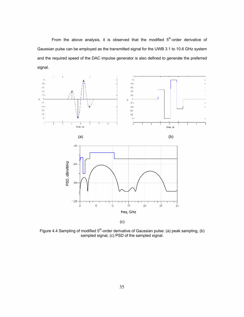
35
From the above analysis, it is observed that the modified 5th-order derivative of
Gaussian pulse can be employed as the transmitted signal for the UWB 3.1 to 10.6 GHz system
and the required speed of the DAC impulse generator is also defined to generate the preferred
signal.
(a) (b)
(c)
Figure 4.4 Sampling of modified 5th-order derivative of Gaussian pulse: (a) peak sampling, (b) sampled signal, (c) PSD of the sampled signal.
36
(a)
(b)
Figure 4.5 Effect of parasitic on sampled signal: (a) transient response, (b) PSD of the sampled signal.
4.1.3 DAC-Based Impulse Generator Architecture
Resistor-based and current-steering are two major types for the DAC design. To
achieve high speed operation, the current-steering DAC architecture is chosen for this design.
In the current-steering DAC, the glitches are a major limitation for high speed operations from
the timing skews of the digital switching signals [43], [44]. As illustrated in Figure 4.6 [43], a
simple binary weighted 4-bit DAC is considered. Suppose the binary digital switching inputs are

37
switching from 1000 to 0111 and thus the output is connected from only the most significant bit
(MSB) current source to only the three remaining current source with one IRL level change.
However, once the digital input signals driving the switches suffer from finite rising and falling
time as well as timing skews, all four current sources maybe partially off or on for a short time
during the transition from 1000 to 0111 and causing glitches at the output. Thus, to reduce the
glitch, it is desired to have less number of current switching during transitions.
8I 4I 2I 1I 8I 4I 2I 1I
RL RLtransition
(a)
-8IRL
-7IRL
(b)
Figure 4.6 Glitch in current-steering DAC: (a) transition from 1000 to 0001, (b) output glitch.
For this design, since the designated modified 5th-order derivative of Gaussian pulse
has only five magnitudes levels in the waveform, it can be generated using a 3-bit DAC. The
architecture of the impulse generator is shown in Figure 4.7, which consists of one load resistor
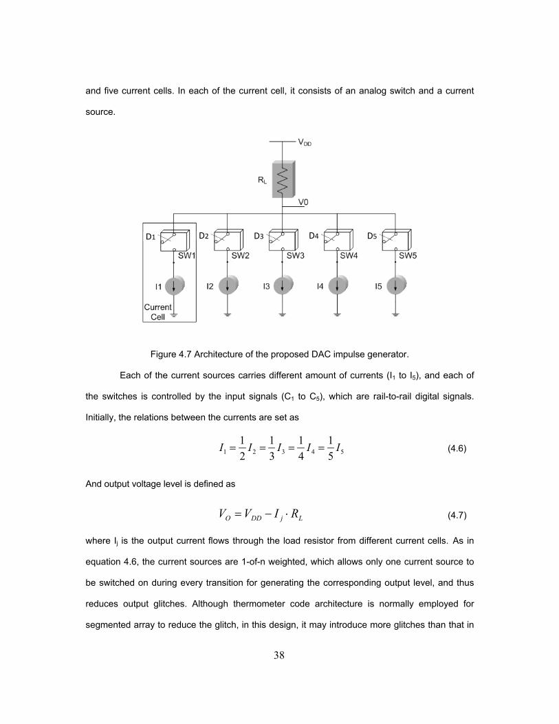
38
and five current cells. In each of the current cell, it consists of an analog switch and a current
source.
D1 D2 D3 D4 D5
Figure 4.7 Architecture of the proposed DAC impulse generator.
Each of the current sources carries different amount of currents (I1 to I5), and each of
the switches is controlled by the input signals (C1 to C5), which are rail-to-rail digital signals.
Initially, the relations between the currents are set as
54321 51
41
31
21 IIIII ==== (4.6)
And output voltage level is defined as
LjDDO RIVV ⋅−= (4.7)
where Ij is the output current flows through the load resistor from different current cells. As in
equation 4.6, the current sources are 1-of-n weighted, which allows only one current source to
be switched on during every transition for generating the corresponding output level, and thus
reduces output glitches. Although thermometer code architecture is normally employed for
segmented array to reduce the glitch, in this design, it may introduce more glitches than that in
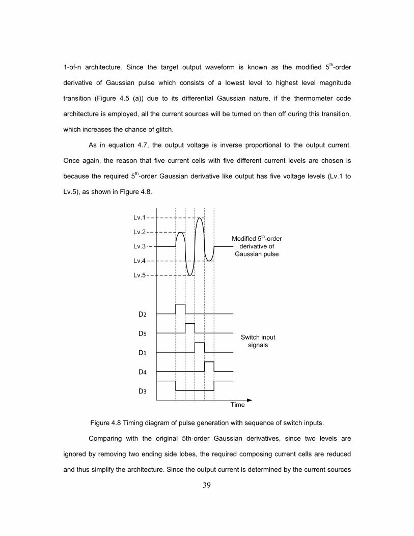
39
1-of-n architecture. Since the target output waveform is known as the modified 5th-order
derivative of Gaussian pulse which consists of a lowest level to highest level magnitude
transition (Figure 4.5 (a)) due to its differential Gaussian nature, if the thermometer code
architecture is employed, all the current sources will be turned on then off during this transition,
which increases the chance of glitch.
As in equation 4.7, the output voltage is inverse proportional to the output current.
Once again, the reason that five current cells with five different current levels are chosen is
because the required 5th-order Gaussian derivative like output has five voltage levels (Lv.1 to
Lv.5), as shown in Figure 4.8.
D1
D2
D3
D4
D5
Figure 4.8 Timing diagram of pulse generation with sequence of switch inputs.
Comparing with the original 5th-order Gaussian derivatives, since two levels are
ignored by removing two ending side lobes, the required composing current cells are reduced
and thus simplify the architecture. Since the output current is determined by the current sources
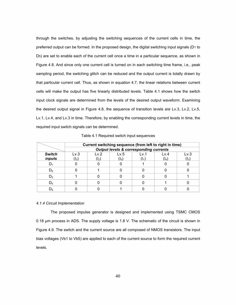
40
through the switches, by adjusting the switching sequences of the current cells in time, the
preferred output can be formed. In the proposed design, the digital switching input signals (D1 to
D5) are set to enable each of the current cell once a time in a particular sequence, as shown in
Figure 4.8. And since only one current cell is turned on in each switching time frame, i.e., peak
sampling period, the switching glitch can be reduced and the output current is totally drawn by
that particular current cell. Thus, as shown in equation 4.7, the linear relations between current
cells will make the output has five linearly distributed levels. Table 4.1 shows how the switch
input clock signals are determined from the levels of the desired output waveform. Examining
the desired output signal in Figure 4.8, the sequence of transition levels are Lv.3, Lv.2, Lv.5,
Lv.1, Lv.4, and Lv.3 in time. Therefore, by enabling the corresponding current levels in time, the
required input switch signals can be determined.
Table 4.1 Required switch input sequences
Current switching sequence (from left to right in time) Output levels & corresponding currents
Switch inputs
Lv.3 (I3)
Lv.2 (I2)
Lv.5 (I5)
Lv.1 (I1)
Lv.4 (I4)
Lv.3 (I3)
D1 0 0 0 1 0 0 D2 0 1 0 0 0 0 D3 1 0 0 0 0 1 D4 0 0 0 0 1 0 D5 0 0 1 0 0 0
4.1.4 Circuit Implementation
The proposed impulse generator is designed and implemented using TSMC CMOS
0.18 μm process in ADS. The supply voltage is 1.8 V. The schematic of the circuit is shown in
Figure 4.9. The switch and the current source are all composed of NMOS transistors. The input
bias voltages (Vb1 to Vb5) are applied to each of the current source to form the required current
levels.

41
RL
Cb
Nc1 Nc2 Nc3 Nc4 Nc5
Vb1 Vb2 Vb3 Vb4 Vb5
D2Ns1
D1Ns2 Ns3 Ns4 Ns5
D3 D4 D5
1.8V
50 Ω
Vout
Figure 4.9 Schematic of the proposed DAC impulse generator.
In each of the current cell, transistors in the current source (Ncj) and the switch (Nsj)
form a cascode stage, and thus the output impedance of each current cell can be expressed as
1,2,3,4,5j rorogmR CjSjSjjout =⋅⋅= ;_ (4.8)
where gmS is the transconductance of the switch transistor and roSj and roCj are the intrinsic
output resistances of the switching transistor and current source transistor, respectively.
Equation 4.8 is obtained by assuming both the transistors are in saturation region, which is the
preferable condition to maintain larger output impedance. If the switching transistor is in deep
triode region, the output impedance will be reduced to
1,2,3,4,5j RroR onSjCjjout =+= ;_ (4.9)

42
where RonS is the on-resistance. The high output impedance of the current cell can improve the
linearity of the circuit. The nonlinearity of the circuit mainly comes from two contributions: first,
the output current variation caused by the finite output resistance in each current cell from the
output voltage variation; second, the output voltage variation due to different output impedances
in each current cell when loading to the output. To clarify these nonlinearity contributions,
consider the equivalent small signal model of the DAC impulse generator as illustrated in Figure
4.10, where roCj represents the output resistance of each current source in saturation and R1 is
the equivalent resistance from parallel combination of RL and 50-Ω load. Thus, the output
voltage can be found as
1,2,3,4,5j RroIjV Cjout =⋅⋅−= );//( 1 (4.10)
where roCj in each current source are different because different currents are supplied.
Figure 4.10 Equivalent small signal circuit of proposed DAC impulse generator.
During the impulse generating operation, as different currents drawn from different
current sources, different roCj are loaded from output to ground causing integral nonlinearity to
the output, which comes from the dependence of the term in parentheses in equation 4.10.
Moreover, roCj and supplied currents in each current source vary with different level of output
voltage because of the short-channel effect causing nonlinearity also. Thus, these imply that the

43
high output impedance can improve the linearity by suppressing variations at the output and
making the current source more ideal.
Therefore, for sizing the transistors, the length of current source transistors (Ncj) and
width of switch transistors (Nsj) are chosen to increase the output impedance while the length of
current source transistors is also adjusted inverse proportionally to their supply currents
compensating the effect on roCj variations. To achieve high speed, the length of switch
transistors is kept as minimum. The current source itself may be employed as a cascode stage
to further increase the output impedance, but the output voltage headroom will be limited. Thus,
the simple two transistors stack in each of the current cell allows the large voltage swing of the
output and also reduces the capacitance from the transistors, then increases the speed. Since
the output pulse repetition frequency (PRF) can be tuned by the switch input signals while the
output swing can be tuned by the current source bias voltages, the proposed impulse generator
has a high-tunability to generate various outputs with different data rate while sufficiently
complying with the FCC regulations.
4.1.5 Digital Switch Control Signals
As illustrated in Figure 4.8 in the previous section, to properly generate the preferred
impulse signal, particular sequences of digital switch control signals have to be generated (Dj).
These low duty cycle digital pulses can be generated using digital logic circuits without the need
of high-speed digital processing and programming unit, as shown in Figure 4.11 (a). The digital
pulses generator contains two AND gates, two NOR gates, four buffering inverter, and one
XNOR gate. The input-output timing diagrams are shown in Figure 4.11 (b). The sequence of
digital switch control pulses is generated at every rising edge of the input master clock signal.
The master clock signal is sequentially delayed and inverted through buffering inverters and
sent to each logic gate to produce the corresponding output signal. Thus, the output pulse width
is controlled by the buffering inverters, which is also the DAC sampling period.

44
AND
AND
NOR
NOR
XNOR
D2
D5
D1
D4
D3
D2D5D1D4
CLKA
B
C
D
CLK
A
B
C
D
D2
D5
D1
D4
D3
(a) (b)
Figure 4.11 Generation of digital switch control signals: (a) digital circuit implementation, (b) timing diagrams.
Nonetheless, to maximally reduce the output glitches, the need of precisely timed
edges of digital switch control signals is critical especially for the high-speed application. As
depicted in Figure 4.12, the rising and falling time of each switch control signal are synchronized
at the 50 % voltage points to ensure that the switches are turned on and off simultaneously.
For this design, to prove the concept of DAC impulse generation, the logic circuits and
digital control signals are implemented and simulated using simulink in Matlab.

45
D1
D2
Figure 4.12 Synchronization of switch control signals.
4.1.6 Modulation Capability
4.1.6.1 OOK
Since the digital control signals are generated only on every rising edge of the input
clock signal, which means that the DAC impulse generator also generates output on every
rising edge of the input clock, the proposed DAC impulse generator can simply employ OOK at
the input digital domain. For example, as shown in Figure 4.13 (a), the input clock signal is sent
to the OOK modulator with the digital data stream, which generates the modulated digital trigger
signal as the input of the switch control signals generator. Thus, the DAC impulse generator
generates the output on the rising edges of the trigger signal realizing the OOK as shown in
Figure 4.13 (b). Because the modulation is done in digital domain before the impulse signal
generation, it much alleviates the design requirements on the modulator. If the modulation is
done in RF domain after the impulse generation, a RF modulator is required with the need of
large bandwidth and higher power. Furthermore, as in Figure 4.13 (b), the modulated signal is
actually a return-to-zero data, which means that the proposed DAC impulse generator can be
triggered directly by the return-to-zero clocked data without the need of additional master clock
signal and modulator.

46
Input data
OutputDAC Impulse Generator
Switch Control Signals
Generator
CLKOn-OffKeying
Modulator
Trigger
(a)
Input data
CLK
Trigger
Output
1 1 0 1 0
(b)
Figure 4.13 OOK: (a) block diagram, (b) timing diagrams.
4.1.6.2 BPM
To achieve bi-phase modulations, the differential output impulses have to be generated.
The proposed DAC impulse generator can be implemented as a differential architecture. As
shown in Figure 4.14, the switch in each of the current cells is replaced by a differential pair of
transistors comparing with that in the single-ended DAC impulse generator. The differential
switches are driven by the differential control signals (Dj, Dj¯ ). The differential swing between the
control signals has to be large enough to ensure that one branch turns off completely for the
maximum output swing. The differential control signals also need precisely synchronized edges
to drive the differential switches on and off simultaneously.

47
RL
Cb
Nc1
Vb1
Ns1D1
Ns2
1.8V
50 Ω
Vout
D1
RL
Cb
50 Ω
Vout
Nc2
Vb2
Ns3D2 Ns4D2
Nc3
Vb3
Ns5D3 Ns6D3
Nc4
Vb4
Ns7D4 Ns8D4
Nc5
Vb5
Ns9D5 Ns10D5
Figure 4.14 The differential DAC impulse generator.
The sizing of transistors for the differential DAC impulse generator follows the same
principle as that for the single-ended topology while the size of transistors in each differential
switch is kept the same for the fully symmetrical implementation. However, recall that for Dj, the
signals are generated to ensure that only the corresponding one of five current sources
connects to the output at a time (Table 4.1), and thus the differential Dj¯ signals make four
current sources connect to the output at a time instead. Therefore, the common mode voltage
at
Since the differential signals are generated in RF domain, a RF modulator (e.g., a RF
switch) is needed to process these differential impulse signals and pass either one of them to
the output according to the state of the data stream. The differential architecture also consumes
more power than that of the single-ended architecture because each current source is always
steering to either one of the differential branches. Thus, when one of the differential outputs is
Vout before Cb is lower than that at Vout before Cb causing smaller allowable output swing to
prevent transistors in triode region, which means the current supplied in each of the current
sources is smaller than that in the single-ended architecture.
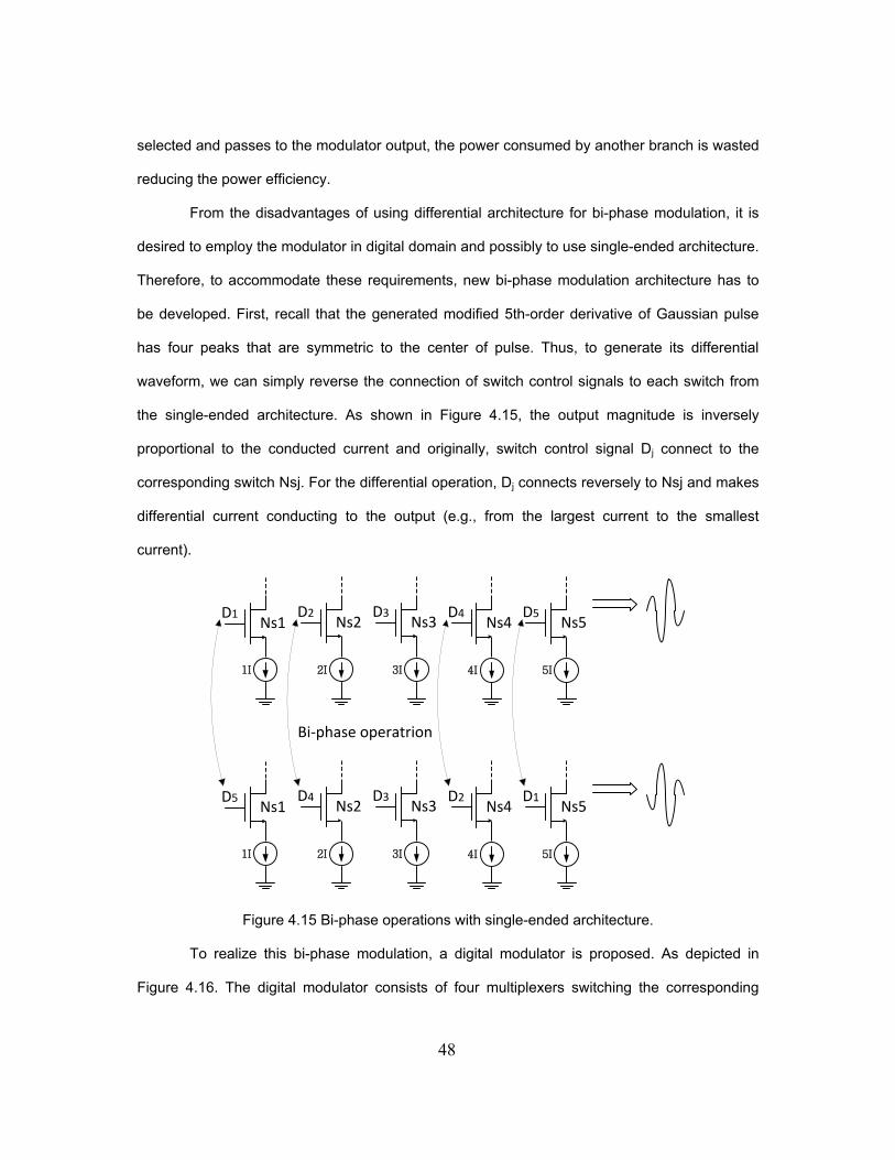
48
selected and passes to the modulator output, the power consumed by another branch is wasted
reducing the power efficiency.
From the disadvantages of using differential architecture for bi-phase modulation, it is
desired to employ the modulator in digital domain and possibly to use single-ended architecture.
Therefore, to accommodate these requirements, new bi-phase modulation architecture has to
be developed. First, recall that the generated modified 5th-order derivative of Gaussian pulse
has four peaks that are symmetric to the center of pulse. Thus, to generate its differential
waveform, we can simply reverse the connection of switch control signals to each switch from
the single-ended architecture. As shown in Figure 4.15, the output magnitude is inversely
proportional to the conducted current and originally, switch control signal Dj connect to the
corresponding switch Nsj. For the differential operation, Dj connects reversely to Nsj and makes
differential current conducting to the output (e.g., from the largest current to the smallest
current).
D2 Ns2D1 Ns1 Ns3 D4 Ns4D5 Ns5
D3
Bi-phase operatrion
1I 2I 3I 4I 5I
D4 Ns2D5 Ns1 Ns3 D2 Ns4D1 Ns5
D3
1I 2I 3I 4I 5I
Figure 4.15 Bi-phase operations with single-ended architecture.
To realize this bi-phase modulation, a digital modulator is proposed. As depicted in
Figure 4.16. The digital modulator consists of four multiplexers switching the corresponding
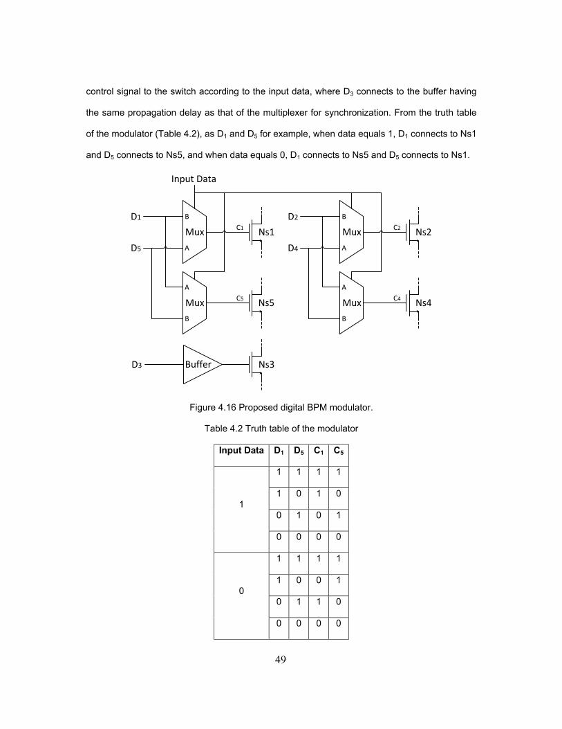
49
control signal to the switch according to the input data, where D3 connects to the buffer having
the same propagation delay as that of the multiplexer for synchronization. From the truth table
of the modulator (Table 4.2), as D1 and D5 for example, when data equals 1, D1 connects to Ns1
and D5 connects to Ns5, and when data equals 0, D1 connects to Ns5 and D5 connects to Ns1.
D5
D1
Ns1
Ns5
Mux
Mux
B
A
A
B
D3 Ns3Buffer
D4
D2
Ns2
Ns4
Mux
Mux
B
A
A
B
Input Data
C1 C2
C5 C4
Figure 4.16 Proposed digital BPM modulator.
Table 4.2 Truth table of the modulator
Input Data D1 D5 C1 C5
1
1 1 1 1
1 0 1 0
0 1 0 1
0 0 0 0
0
1 1 1 1
1 0 0 1
0 1 1 0
0 0 0 0

50
The proposed digital modulator accomplishes the bi-phase modulation in digital domain
with single-ended DAC impulse generator having lower power consumption, higher power
efficiency, and larger output swing than that of the differential architecture. Like the switch
control signal generator, the digital modulator is also implemented and simulated with simulink
in Matlab.
4.2 Simulation of Proposed IR-UWB Impulse Generator
4.2.1 Single-Ended DAC Impulse Generator
The simulations of proposed DAC impulse generator have been done in ADS. There
are two sets of outputs with different PRFs. In Figure 4.17, the generated modified 5th-order
derivative of Gaussian pulse and its PSD are shown.
(a) (b)
Figure 4.17 Simulation of single-ended DAC impulse generator output with PRF of 50 MHz: (a) transient response, (b) PSD.
The output has a 320 ps pulse width, 335 mV peak-to-peak voltage with a 50 MHz PRF.
The PSD of the output complies with the FCC mask and has a center frequency of 6.7 GHz and
a -10dB bandwidth from 3.4 GHz to 10.3 GHz. In Figure 4.18, the generated output has a 310
ps pulse width, 86 mV peak-to-peak voltage with a 100 MHz PRF. And the PSD of the output
also complies with the FCC regulation and has a center frequency of 6.7 GHz and a -10 dB
bandwidth from 3.6 GHz to 10.2 GHz. The power consumptions are 27 mW at a PRF of 50 MHz
and 28 mW at a PRF of 100 MHz. The simulation results show that the proposed design has the

51
ability to adjust the outputs with respect to different PRF while the outputs sufficiently utilize the
spectrum and meet the FCC mask.
(a) (b)
Figure 4.18 Simulation of single-ended DAC impulse generator output with PRF of 100 MHz: (a) transient response, (b) PSD.
4.2.2 Single-Ended DAC Impulse Generator with OOK
To verify the OOK capability of the circuit, the return-to-zero coded data is employed as
the input of the switch control signals generator. As shown in Figure 4.19, the output impulses
are triggered/generated on every rising edge of the input data and thus it is proven that the
proposed DAC impulse generator can achieve OOK without the need of OOK modulator.
The PSD of the OOK modulated output is also simulated to exam the effect of OOK.
Figure 4.20 shows the comparison of the PSD with and without OOK at the PRF of 50 MHz
while Figure 4.21 shows the comparison at the PRF of 100 MHz. As can be seen, with OOK,
the magnitude and the spectral spikes are reduced, which is the benefit of modulation allowing
either larger output swing (longer transmission range) or higher PRF (faster communication
rate) while meeting the FCC regulation.

52
Figure 4.19 Simulation of OOK output.
(a) (b)
Figure 4.20 Comparison of PSD at PRF of 50 MHz: (a) with OOK, (b) without OOK.
(a) (b)
Figure 4.21 Comparison of PSD at PRF of 100 MHz: (a) with OOK, (b) without OOK.

53
4.2.3 Differential DAC Impulse Generator
As shown in Figure 4.22, the differential architecture generates the differential outputs
with a maximum swing of 135 mV which is smaller than that of the single-ended output. The
PSD is simulated at a PRF of 50 MHz and the total power consumption is 48 mW.
(a) (b)
Figure 4.22 Simulation of differential DAC impulse generator: (a) transient response, (b) PSD.
4.2.4 Single-Ended DAC Impulse Generator with Bi-Phase Modulator
The BPM modulator is simulated in simulink with the co-simulation of the single-ended
DAC impulse generator in ADS. As shown in Figure 4.23, with synchronization of the input data
and the master clock, the bi-phase output impulses are generated on every rising edge of the
input data. To facilitate the observation on bi-phase signals, PRF of 1 GHz is employed, which
also means the proposed impulse generator can work properly at high data rates.

54
Figure 4.23 Simulation of bi-phase modulation output at PRF of 1 GHz.
The PSD of the BPM modulated output is also simulated. Figure 4.24 shows the
comparison of the PSD with and without BPKK modulation at the PRF of 50 MHz while Figure
4.25 shows the comparison at the PRF of 100 MHz. Again, it is observed that with the
modulation, the magnitude and the spectral spikes are reduced.
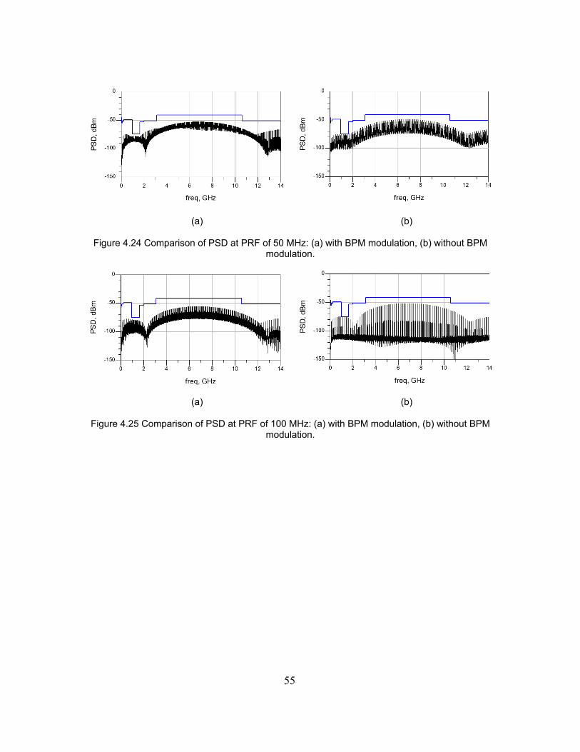
55
(a) (b)
Figure 4.24 Comparison of PSD at PRF of 50 MHz: (a) with BPM modulation, (b) without BPM modulation.
(a) (b)
Figure 4.25 Comparison of PSD at PRF of 100 MHz: (a) with BPM modulation, (b) without BPM modulation.

56
CHAPTER 5
A FULLY INTEGRATED CMOS UWB FILTERING-TYPE IMPULSE GENERATOR
As mentioned in Chapter 3, for the UWB impulse generator, the passive filtering method
is attractive for its low power and low complexity potentialities. A passive filtering type IR-UWB
impulse generator with a simpler architecture is presented in this chapter to resolve the high
complexity and high power consumption of the existing filtering methods employing least
number of transistors and passives compared with other filtering methods. It is fully
implemented using 90 nm CMOS technology for high performance and low power. As a result,
the proposed impulse generator can achieve low cost, low power, and low complexity for the
3.1-10.6 GHz UWB systems.
5.1 Design of Proposed IR-UWB Impulse Generator
The architecture of the proposed design is shown in Figure 5.1, which consists of three
parts: a Gaussian pulse generator, a pulse shaper, and an antenna load. The Gaussian pulse
generator is designed employing a modified-XOR gate which has the simpler architecture than
the traditional one using delay cells and XOR gate [45]. The pulse shaper built by the band-pass
filter (BPF) reshapes the baseband output pulse train from the pulse generator and make its
center frequency reside in the designated frequency band. For the antenna load, the realistic
passive antenna model is used in the simulation instead of the typical 50 Ω to determine the
minimum order of BPF that can satisfy the FCC power emission regulation since the antenna
alters the bandwidth and the center frequency of output power spectrum. Unlike the proposed
DAC impulse generator in Chapter 4, the filtering-type impulse generator realizes the impulse
generation with frequency-domain approach instead of time-domain approach. The proposed
simplex architecture of the filtering-type impulse generator increases the speed of the circuit,

57
and also decreases the power consumption. All the circuits are designed using IBM 90 nm
CMOS technology with the supply voltage of 1.2 V.
Figure 5.1 Architecture of the proposed UWB impulse generator.
5.1.1 Impulse Generation Principle
To understand the design principle of the frequency-domain approach of the proposed
impulse generator, the frequency response of each node in the impulse generator has to be
understood. Figure 5.2 illustrates the frequential characteristics of each block output in the
impulse generator. As mentioned in chapter 3.1.1, the output of the Gaussian pulse generator
should have a pulse width narrow enough to have a wide power spectrum covering the
designated frequency band (e.g., 3.1-10.6 GHz) as shown in Figure 5.2 (a). Then, as in Figure
5.2 (b), with considering the antenna effect, BPF should have a center frequency in the middle
of the regulated frequency band, a -3 dB bandwidth within the regulated frequency band, and a
minimum order that provides the enough attenuation response at the stop band to shape the
output spectrum. Finally, the antenna removes the excessive bandwidth and makes the output
spectrum meeting the FCC mask as shown in Figure 5.2 (c). Therefore, the main goal of the
design is to have a BPF output spectrum that sufficiently utilizes the UWB band within the
designated band. Even though the -10 dB bandwidth may be too wide and out of the regulated
band, the antenna will eliminate this excessive bandwidth.

58
Figure 5.2 (a) Gaussian pulse generator output spectrum, (b) BPF frequency response, (c) BPF and antenna output spectrum.

59
5.1.2 Design Parameters and Output PSD
As the design principle is in frequency domain, it is important to investigate the
relationship between the design parameters (e.g., pulse width, magnitude, and PRF) and the
output PSD. As shown in Figure 5.1 above, the Gaussian pulse is generated to excite the BPF.
Thus, the output of the BPF g(t) can be expressed as the convolution of the Gaussian pulse x(t)
and the impulse response of the BPF hb(t); which is given by
)()2
exp(2
)()()(
2
2
thtA
thtxtg
∗−=
∗=
σσπ (5.1)
where A and σ are the magnitude parameter and the pulse width parameter, respectively. Thus,
the Fourier transform of g(t) can be found as
LfHfAfG )()
2exp(
2)(
22
⋅−=σ
π (5.2)
where the first term on the right hand side is the Fourier transform of the Gaussian pulse [27],
and second term is the normalized transfer function with the loss L. It can be seen that the
frequency response of the Gaussian pulse also contains a Gaussian function which is one of
the distinct characteristics of Gaussian pulse.
By assuming BPF output signals is uniformly spaced in time or linearly modulated (e.g.,
OOK, BPM), the output signals can be thus expressed by the autocorrelation function as
∑∞
−∞=
⋅−⋅=k
Pk Tktgats )()( (5.3)
where Tp is pulse repetition interval and the sequence ak represents the information symbol.
The PSD of the BPF output can be therefore found from the Fourier transform of the above
autocorrelation function and can be expressed using the equation 3.6 in Chapter 3. By
evaluating the spectrum at f=j/Tp and applying equation 5.2 into equation 3.6, we can find the
expression of BPF output PSD with design parameters as

60
−+⋅
⋅⋅
⋅−=
−+⋅=
−+=
∑
∑
∑
∞
−∞=
∞
−∞=
∞
−∞==
j pp
aa
p
j pp
aa
p
j ppp
a
p
aTjf
Tjf
TTL
fHfA
Tjf
TTfG
Tjf
TjG
TfG
TfPSD
p
)(1
)()2
exp(2
)()(
)()()(),(
22
222
22
2
2
2
22
2
/
δµσ
σπ
δµσ
δµσ
(5.4)
from equation 5.4, it appears that the magnitude of the PSD linearly depends on A, Tp, and L
when Gaussian pulse width and BPF response are fixed. As Gaussian pulse width is small; σ is
small, the exponential function has a flat decay in frequency producing power spectrum at the
higher frequency. Once this frequency is larger than the upper cutoff frequency of the BPF, the
bandwidth and the center frequency of the output PSD is determined by H(f). Otherwise, if the
Gaussian pulse width is large, exponential function will introduce a fast decay in frequency and
output bandwidth and center frequency will be reduced and determined by the degree of this
spectrum decay.
To illustrate the above statement, normalize Gaussian pulses with different pulse widths
are sent to an ideal first order Butterworth BPF with 3 GHz bandwidth. The resulting normalized
PSDs are shown in Figure 5.3. It is observed that when σ is larger than 1e-11, the decaying
response dominates and center frequency as well as bandwidth shift to lower frequency. Note
that the magnitude at lower frequency band of each PSD is higher with larger pulse width. It is
because with the same normalized magnitude, Gaussian pulse with larger pulse width contains
more signal power resulting higher peak PSD magnitude at baseband.

61
Figure 5.3 BPF output PSD with different input Gaussian pulses.
5.1.3 Gaussian Pulse Generator
The purposes of designing the Gaussian pulse generator are to generate the baseband
Gaussian-like pulse with very narrow pulse-width while having the capability to drive the next
stage and to reduce the power consumption from its simple structure. For high-speed operation,
it is normal to use current-mode logic (CML) circuits for pulse generation. For example, a CML
inverter is shown in Figure 5.4. Although the logic transition time can be decreased with this
source-coupled current-mode architecture, the power consumption is high because of the static
power from the constant current flowing through Vdd and the digital output swing is limited by
the minimum overdrive voltages across switching transistors (N1, N2) and the current source.
By employing the CML circuits as a Gaussian pulse generator, the constrained output
magnitude results a limited output power spectrum magnitude, as mentioned in the previous
subsection. Therefore, the driving capacity, as well as the peak power, can be improved by
using rail-to-rail logic.
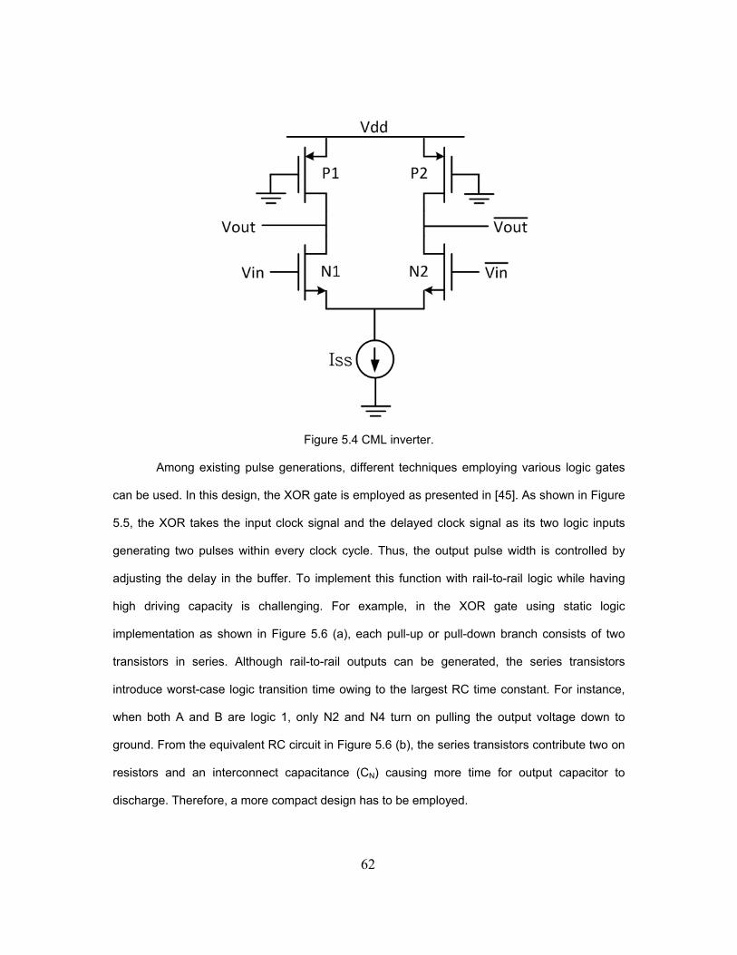
62
Figure 5.4 CML inverter.
Among existing pulse generations, different techniques employing various logic gates
can be used. In this design, the XOR gate is employed as presented in [45]. As shown in Figure
5.5, the XOR takes the input clock signal and the delayed clock signal as its two logic inputs
generating two pulses within every clock cycle. Thus, the output pulse width is controlled by
adjusting the delay in the buffer. To implement this function with rail-to-rail logic while having
high driving capacity is challenging. For example, in the XOR gate using static logic
implementation as shown in Figure 5.6 (a), each pull-up or pull-down branch consists of two
transistors in series. Although rail-to-rail outputs can be generated, the series transistors
introduce worst-case logic transition time owing to the largest RC time constant. For instance,
when both A and B are logic 1, only N2 and N4 turn on pulling the output voltage down to
ground. From the equivalent RC circuit in Figure 5.6 (b), the series transistors contribute two on
resistors and an interconnect capacitance (CN) causing more time for output capacitor to
discharge. Therefore, a more compact design has to be employed.

63
XORCLK
Buffer
AOut
CLK
A
Out
Figure 5.5 Pulse generations with XOR gate.
Vdd
BN3 N4
P1 P2
AN1 N2
P3 P4
A
B
B
A
A
B
A B
Cout
CN
RN2
RN4
Vout
+
-
Idis
(a) (b)
Figure 5.6 Static logic XOR gate: (a) circuit implementation, (b) RC equivalent circuit.
In [46], a compact XOR circuit is presented as shown in Figure 5.7 (a). Although the
circuit contains only one pull-up/pull-down transistor, the output magnitude is irregular from
different input logic combinations. As illustrated in Figure 5.7 (b), by assuming output is at logic
1 initially, when A and B are 0, P2 turns on pulling output to logic 0. However, since P2 requires

64
minimum |Vgs| as its threshold voltage |Vtp| to keep it conducting, the minimum output level is
|Vtp|. The similar problem happens when A is 0 and B is 1, where N2 is conducting and pulling
logic 1 to the output. The maximum output is Vdd-Vtn as output node becomes the source of N2
requiring minimum Vgs as Vtn. Therefore, while this compact XOR gate may work with other
logic function gates with proper phase margin design, it can be hardly used as the Gaussian
pulse generator.
(a) (b)
Figure 5.7 Compact XOR gate: (a) circuit implementation, (b) timing diagram.
To eliminate the problems from the above compact XOR gate while achieving proper
Gaussian pulse generation, a novel pulse generator is therefore proposed. The pulse generator
is implemented by embedding delay cells into a XOR gate resulting in the modified compact
XOR gate as shown in Figure 5.8 (a). The delay cell contains two CMOS inverters (P1, N1 and
P2, N2) in series followed by the third inverter (P3, N3) as the modified compact XOR gate. The
input to the third inverter is the delayed pulse while the original input clock signal is supplied as
the Vdd (another input) to the third inverter. Output of the third inverter is “1” only when its Vdd
is “1” and its input is “0”, and thus the modified XOR function can be formed to generate the
desired pulse on every rising-edge of the input clock, as shown in Figure 5.8 (b) for the output
timing diagram. Comparing to the compact XOR gate in Figure 5.7, since source of the NMOS
here in the last inverter is connected to ground instead of A , the output pulse with constrained

65
magnitude Vdd-Vtn can be eliminated. The modified XOR function can be therefore expressed
as
BA
BBA
A BABABA m
⋅=
⋅+⋅=
=⋅+⋅=⊕
0
0;
(5.5)
However, as mentioned above, when the input to the third inverter and its Vdd are both 0 and
the output has an initial voltage larger than |Vtp|, the output voltage is constrained to |Vtp| instead
of zero. Moreover, when the output has an initial voltage smaller than |Vtp| instead, both PMOS
and NMOS in the third inverter are not conducting and the output node is floating. At this
moment, the output voltage is very susceptible to noise and clock feedthrough during high-
speed switching. Thus, a discharge path has to be provided to the output node to solve above
problems. In this design, this is accomplished by connecting a NMOS (N4) after the third
inverter and uses the output of the first inverter as its gate input.
The proposed simplex architecture can has the faster speed and smaller input
capacitance than the conventional XOR circuit, since the later has a stack of two transistors on
both NMOS and PMOS sides, which increases the rise and fall time of the pulse. Therefore, the
generated output Gaussian-like pulses can have a very narrow pulse width and have a very
wide spectrum bandwidth. Moreover, since the pulse generation is designed to generate the
pulse only on every rising-edge of the input clock signal, the power dissipation can be
eliminated comparing to the normal XOR gate. Hence, the total power consumption can be
reduced within one clock period.

66
Figure 5.8 (a) Schematic of the proposed Gaussian pulse generator, (b) timing diagram of the pulse generator out.
For designing the pulse generator and choosing the proper transistor sizes, the
required output pulse shape is first determined. The output magnitude should be rail-to-rail and
the pulse width should make the power spectrum covering the regulated UWB band. As shown
in Figure 5.9, by simulating the Gaussian pulse equation, the required pulse has the magnitude
of 1.2 V (Vdd) and pulse width of 0.16 ns to have a -10 dB bandwidth at about 10.6 GHz which
is the upper limit of the UWB band.
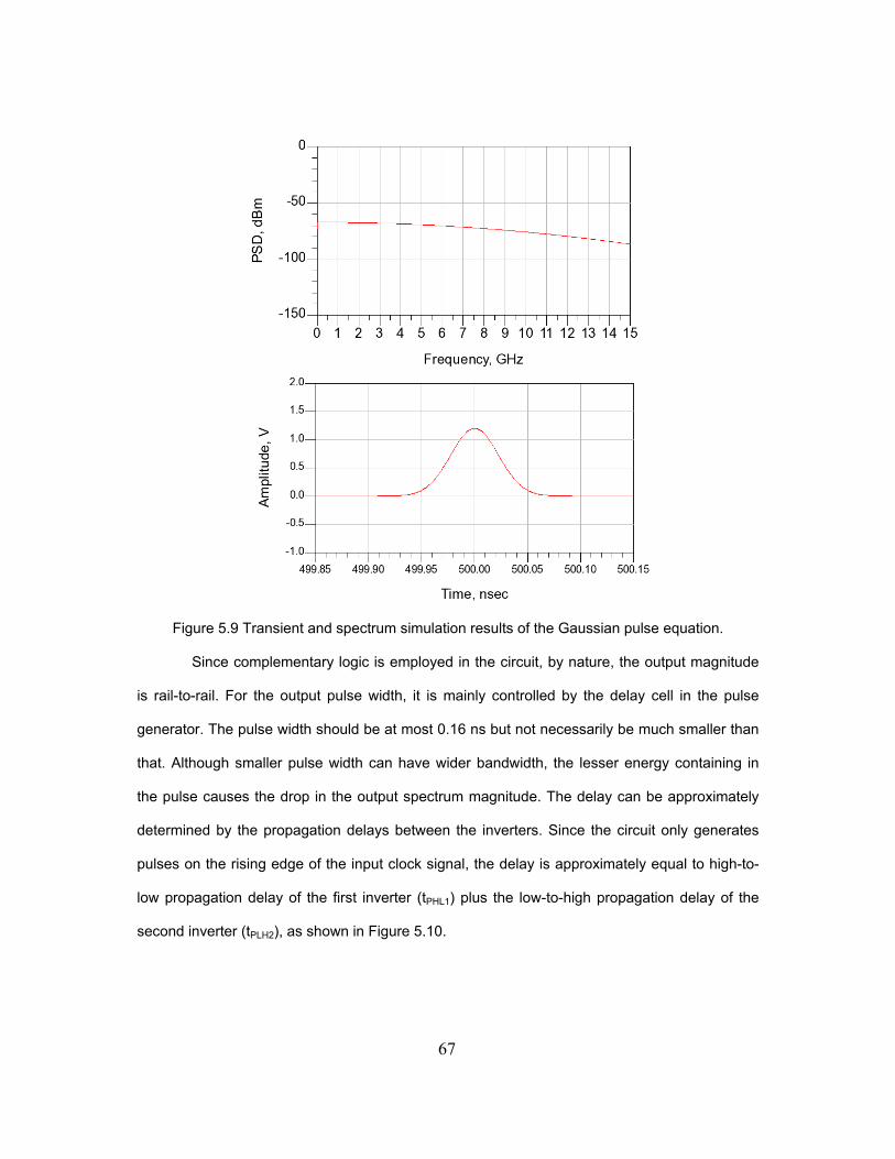
67
Figure 5.9 Transient and spectrum simulation results of the Gaussian pulse equation.
Since complementary logic is employed in the circuit, by nature, the output magnitude
is rail-to-rail. For the output pulse width, it is mainly controlled by the delay cell in the pulse
generator. The pulse width should be at most 0.16 ns but not necessarily be much smaller than
that. Although smaller pulse width can have wider bandwidth, the lesser energy containing in
the pulse causes the drop in the output spectrum magnitude. The delay can be approximately
determined by the propagation delays between the inverters. Since the circuit only generates
pulses on the rising edge of the input clock signal, the delay is approximately equal to high-to-
low propagation delay of the first inverter (tPHL1) plus the low-to-high propagation delay of the
second inverter (tPLH2), as shown in Figure 5.10.

68
Figure 5.10 Propagation delay in the delay cell.
The propagation delays, tPHL1 and tPLH2, are defined as the time interval between 50%
voltage points of input and output of each inverter. The formulations of the propagation delays
can be found [46] by
)2ln(5.0
ln 111 nDD
DDnPHL V
Vt ττ =
= (5.6)
where
)( 1
1
1'
11
TnDDn
nn
outn
VVLWK
C
−=τ (5.7)
)2ln(5.0
ln 222 pDD
DDpPLH V
Vt ττ =
= (5.8)
where
)( 2
2
2'2
21
TpDDp
pp
outp
VVLW
K
C
−=τ (5.9)
In equation 5.7, Cout1, the total capacitance seen at output of first inverter, contains the gate-
drain and drain-bulk capacitances contributed from the transistors in the first inverter plus the
gate capacitances from the second inverter. While in equation 5.9, Cout2 contains the gate-drain
and drain-bulk capacitances from the transistors in the second inverter plus the gate

69
capacitances from the third inverter. Thus, by proper sizing the transistors (Wn1, Wp2), the
desired delay can be achieved. However, since third inverter, working as the modified XOR,
also contributes the propagation delay to the final output pulse width, the transistor size of the
third inverter should be determined first with the output load capacitance to minimize the
propagation delay. Then, with considering the propagation delay of the third inverter, the delay
from the first two inverters can be determined.
5.1.4 Band-Pass Filter
The BPF is designed to have less number of orders limiting the loss in the filter,
occupying less chip area, and to shape the output bandwidth that allocates the center frequency
within 3.1-10.6 GHz band. As shown in the schematic of the filter in Figure 5.11, the first-order
Butterworth BPF consisting of a resistor, an inductor, and a capacitor is chosen in this design.
The Butterworth filter can have smooth response in both pass-band and stop-band while
providing sufficient attenuation (roll-off) beyond pass-band. The first-order BPF is chosen
considering the effect of the antenna load to satisfy the FCC power regulation. The s-domain
transfer function of the filter is defined as in
)/1()/1(
)/1()( 2 LCCRssCRssT++
= (5.10)
Conventionally, higher ordered Butterworth BPF is designed and transformed from the
nominal low-pass filter model using frequency and impedance scaling techniques [47].
However, since first-order Butterworth BPF is used, the passives values can be determined
directly from the equations of center frequency (Fc) and bandwidth (BW) given by
LC
FC π21
= (5.11)
CRR
BWL )(2
1π
= (5.12)
The L and C values are chosen to have center frequency at 6 GHz and to be capable of
driving the antenna load. R is the filter input impedance which determines the filter characteristic

70
impedance matching to the load impedance (RL) once output is terminated. Not only
determining the bandwidth of the filter, the value of R can also give the degree-of-freedom on
choosing L and C values, since for RF application, sometimes the small value of capacitor or
inductor is hard to be fabricated while achieving enough intrinsic quality factor. For this design,
the symmetrical spiral inductor and MIM capacitor are implemented. Although the low order
BPF may have insufficient steep-response at the edges of stop-band, the excessive bandwidth
can be easily filtered out by the following transmitting antenna.
Figure 5.11 Schematic of the first-order Butterworth BPF.
5.1.5 RLC Antenna Model
To incorporate the frequency characteristic in the antenna load, the passive model of a
planner UWB antenna in [48] is applied, since it fits with the real antenna impedance by a large
bandwidth. The passive antenna model allows circuit designers understand the effect of
antenna easily from the simulation and then adjust the other circuit parameters to achieve the
preferred overall output performance. The schematic of the antenna model is shown in Figure
5.12. The LC series resonators (C1L1 and C3L3) and parallel resonators (C2L2 and C4L4) model
the flat printed dipole. The transmission line, transformer, and Cs model the short circuit located
at one end of the dipole, the coupling between the microstrip line and the short circuited dipole,
and the series stub, respectively. And Rrad presents the radiation resistor that the voltage across
can be scaled to the transmitted far field waveform.

71
Figure 5.12 Schematic of RLC antenna model [48].
5.2 Simulation and Measurement Results of Proposed Impulse Generator
5.2.1 Simulation
The proposed UWB impulse generator is fully designed and simulated using IBM 90 nm
CMOS process in Cadence design tool. In Figure 5.13, from the top to bottom, the input clock
signal, delayed clock signal, and the Gaussian pulse generator output are shown. It can be
seen that the proposed modified XOR gate generates signal on every rising edge of the input
clock. The Gaussian pulse output has a pulse width about 0.16 ns and has a rail-to-rail
amplitude of 1.2 V. Figure 5.14 shows the transient output of the impulse generator with the 50-
Ω load termination. The output pulse width is 0.45 ns and peak-to-peak amplitude is 70 mV.
Figure 5.13 Gaussian pulse generator transient output.

72
Figure 5.14 Impulse generator transient output.
The PSD of the impulse generator output 50-Ω load is shown in Figure 5.15 to Figure
5.17 with PRF of 50 MHz, 100 MHz, and 200 MHz, respectively. With higher PRF, the
bandwidth and center frequency are kept the same, which means the proposed impulse
generator can work with higher data rates. The center frequency is about 6 GHz with the
maximum magnitude of -59 dBm/MHz at 50 MHz PRF, -53 dBm/MHz at 100 MHz PRF, and -47
dBm/MHz at 200 MHz PRF. The -10 dB bandwidth is 9.5 GHz.
Figure 5.15 Output PSD with PRF of 50 MHz.

73
Figure 5.16 Output PSD with PRF of 100 MHz.
Figure 5.17 Output PSD with PRF of 200 MHz.
Since the proposed filter-type impulse generator generates output only at the rising
edge of the input clock signal, as the DAC impulse generator in Chapter 4, this impulse
generator can easily adapt OOK in the digital domain or can be directly triggered by return-to-
zero coded data. As shown in Figure 5.18, the OOK modulated output impulses are generated
with the return-to-zero data as the input trigger signal. The PSD of the modulated signals is also
simulated and compared with that of un-modulated signals as shown in Figure 5.19, where the
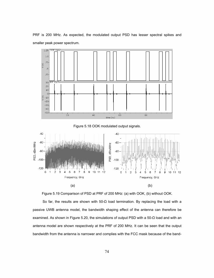
74
PRF is 200 MHz. As expected, the modulated output PSD has lesser spectral spikes and
smaller peak power spectrum.
Figure 5.18 OOK modulated output signals.
(a) (b)
Figure 5.19 Comparison of PSD at PRF of 200 MHz: (a) with OOK, (b) without OOK.
So far, the results are shown with 50-Ω load termination. By replacing the load with a
passive UWB antenna model, the bandwidth shaping effect of the antenna can therefore be
examined. As shown in Figure 5.20, the simulations of output PSD with a 50-Ω load and with an
antenna model are shown respectively at the PRF of 200 MHz. It can be seen that the output
bandwidth from the antenna is narrower and complies with the FCC mask because of the band-

75
pass nature of the antenna. Thus, the first-order BPF employed can meet the FCC power
regulation including the antenna characteristics.
Figure 5.20 PSD of the impulse generator output with 50-Ω load and with RLC antenna model.
5.2.2 Measurement
The proposed UWB impulse generator is fabricated using IBM 90 nm CMOS process.
Figure 5.21 shows the chip photo of the impulse generator and the die area is 0.27 mm2 with
pads. The measurement setup for the impulse generator is shown in Figure 5.22. Tektronix
DG2040 is used as the input clock signal source. For transient response acquisition, the
oscilloscope Agilent DCA 86100B is employed, while the spectrum analyzer Agilent 8563EC is
used for measuring the PSD. Since the UWB antenna is not fabricated for this design, all the
measurements present the results with 50-Ω load terminations as from the instruments.

76
Figure 5.21 Chip photo of the proposed impulse generator.
DUT
Cascade Microtech Probe Station
Tektronix DG2040
Agilent DCA 86100B
Agilent 8563EC
Clock Generator
Spectrum Analyzer
Oscilloscope
Figure 5.22 Measurement setup.
Figure 5.23 shows the measured transient output result of the impulse generator with
50-Ω load termination at 200 MHz PRF, which is consistent with the simulation result. The
output pulse width is 0.45 ns and peak-to-peak amplitude is 68 mV. In Figure 5.24, the
measured output PSDs with 100 MHz and 200 MHz PRF are shown. The center frequency is
about 6 GHz with the magnitude of -56 dBm/MHz at 100 MHz PRF. The center frequency is
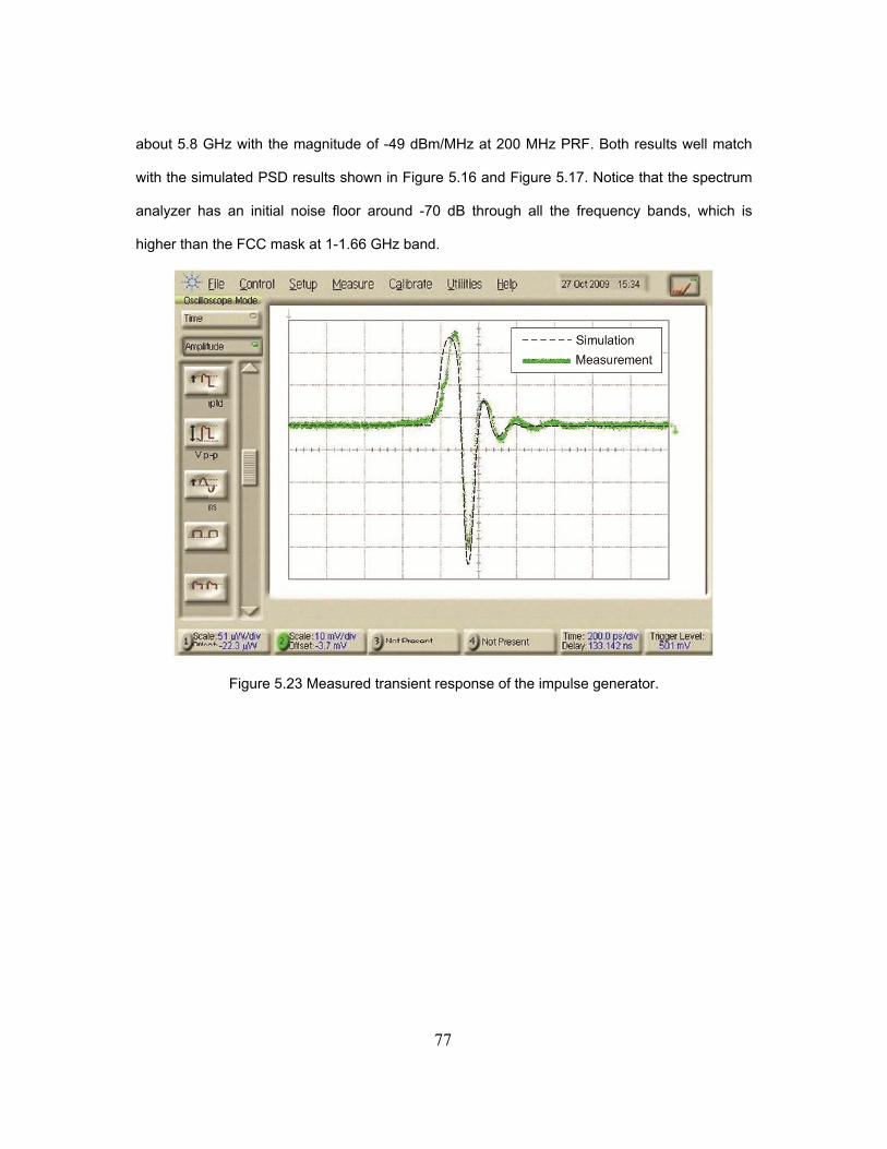
77
about 5.8 GHz with the magnitude of -49 dBm/MHz at 200 MHz PRF. Both results well match
with the simulated PSD results shown in Figure 5.16 and Figure 5.17. Notice that the spectrum
analyzer has an initial noise floor around -70 dB through all the frequency bands, which is
higher than the FCC mask at 1-1.66 GHz band.
Figure 5.23 Measured transient response of the impulse generator.

78
(a)
(b)
Figure 5.24 Measured PSD of the impulse generator output: (a) at 100 MHz PRF, (b) at 200 MHz PRF.

79
Table 5.1 summarizes the performance of the proposed impulse generator compared
with other existing filtering-type impulse generators.
Table 5.1 Comparison table of existing CMOS filtering-type impulse generators
This Work [49] [50] [10] [11] [12] Process 90 nm 0.18 um 0.18 um 0.13 um 0.35 um 90 nm
Filter type Passive BPF
Passive HPF
Passive BPF
Passive BPF
Passive BPF
Active FIR
Output Vpp 70 mV 160 mV 48 mV 1.42 V *18 mV 220 mV Power
consumption 0.9 mW 0.4 mW 1.2 mW 3.84 mW - 227 mW
PRF 200MHz 100MHz - 100 MHz 100 MHz 1.8 GHz
Die area 0.27 mm2 - 0.35 mm2 0.54 mm2 **0.5 mm2 2.83 mm2
Bandwidth 9.2 GHz 6.3 GHz - 6.8 GHz *1.5 GHz 3 GHz * Measured from 1 m distance with antennas.
** Excluding the off-chip BPF.
80
CHAPTER 6
A CARRIER-BASED IMPULSE GENERATOR FOR UWB VEHICULAR SHORT-RANGE RADAR APPLICATION
For UWB vehicular short-range range (SRR) applications, since power consumption is
not the primary concern, the carrier-based systems can provide many benefits over carrier-free
systems as mentioned in Chapter 1. The research and development of the automotive radar
have been undergoing for years after FCC classified the usage of the system. Nonetheless, one
of the main barriers to broadly beneficiate the general public for utilizing this technology has
been the ability to achieve the crucial technical requirements at a low cost level.
Among existing automotive radars, mainly three generic architectures can be
categorized as [36]: 1) frequency chirp radars; 2) continuous wave (CW) pseudorandom noise
(PN) coded radars; and 3) pulsed radar [51]. Frequency chirp radars require a well-defined chirp
to achieve a good resolution and a low phase noise oscillator under the short-range UWB
condition, which is challenging for the cost-effective concern. PN coded radars need high-speed
code generators to be run at a well-defined frequency with a constant offset between one
another requiring extra phased-locked loops. Moreover, PN coded radars have a strict
constraint between dynamic range and the isolation between Tx and Rx antennas from its full-
duplex operation. On the other hand, pulsed radars can realize the cost-effective potentiality
from its simple architecture. The isolation between the Tx and Rx as well as the dynamic range
can also be increased from its pulse-modulated nature. Other benefits of pulsed radars include
good range accuracy, clutter reduction, and multipath resolution [51].
Therefore, a carrier-based impulse generator is proposed for the UWB pulsed radar
systems with simple architecture implementing with cost-effective CMOS technology. The
proposed impulse generator employs the switch-based architecture without using mixer and
power amplifier improving the power consumption and power efficiency. The proposed impulse
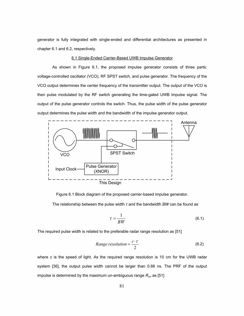
81
generator is fully integrated with single-ended and differential architectures as presented in
chapter 6.1 and 6.2, respectively.
6.1 Single-Ended Carrier-Based UWB Impulse Generator
As shown in Figure 6.1, the proposed impulse generator consists of three parts:
voltage-controlled oscillator (VCO), RF SPST switch, and pulse generator. The frequency of the
VCO output determines the center frequency of the transmitter output. The output of the VCO is
then pulse modulated by the RF switch generating the time-gated UWB impulse signal. The
output of the pulse generator controls the switch. Thus, the pulse width of the pulse generator
output determines the pulse width and the bandwidth of the impulse generator output.
SPST Switch
Antenna
Pulse Generator(XNOR)
VCO
This Design
Input Clock
Figure 6.1 Block diagram of the proposed carrier-based impulse generator.
The relationship between the pulse width τ and the bandwidth BW can be found as
BW1
=τ (6.1)
The required pulse width is related to the preferable radar range resolution as [51]
2τ⋅
=cresolution Range (6.2)
where c is the speed of light. As the required range resolution is 10 cm for the UWB radar
system [36], the output pulse width cannot be larger than 0.66 ns. The PRF of the output
impulse is determined by the maximum un-ambiguous range Run as [51]

82
PRFcRun ⋅
=2
(6.3)
In the case of 25 m as the maximum un-ambiguous range, PRF has to be equal or lesser than 6
MHz. The output of the impulse generator should have a center frequency larger than 24 GHz
and the -10 dB bandwidth within 22-29 GHz as regulated by the FCC.
The VCO, RF switch and the pulse generator are fully designed and implemented using
CMOS 130 nm technology with the supply voltage of 1.2 V. The design and circuit description of
each component are presented in the following subsections.
6.1.1 VCO
VCO is one of the most important components in the radar and communication
applications such as the recovery clock and frequency translation, the output frequency of the
ideal VCO is a linear function of the control voltage. VCO is divided on the two major groups,
resonator less oscillators and resonator oscillators. Ring oscillator and the relaxation oscillator
are common examples for the resonator less oscillator [52]. Although ring oscillator and the
relaxation oscillator have excellent capability in the integration and tunability, these oscillators
suffer from the poor phase noise, stability and quality factor so they are not used in the RF
circuit [52], [53]. In contrast, the resonator oscillators have better phase noise and stability
making them preferable in the RF circuit. A good example of the resonator oscillator is LC tank
circuit, where the periodic signal is excited by switching back and forth from a magnetic field
made from an inductor to an electric field enabled by a capacitor.
In this design, a NMOS cross-coupled LC VCO is employed with the output buffer as
shown in Figure 6.2. The VCO has a differential topology, which greatly rejects the undesired
common-mode disturbances from other building blocks on the same substrate providing better
noise immunity. The minimal number of active components employed helps in reduction of
transistor parasitic which constitute nonlinear capacitors making the VCO frequency shifted as
supply varies introducing extra noise translations. The minimal number of passive components

83
employed helps reducing the chip area and maximizing the Q of the tank, and thus the phase
noise. The output swing can be also maximized at voltage-limit region.
Vdd
Vb
Cvaractor
L
M1 M2
M3
M4
L
Ls
Vout
VCO Buffer
Figure 6.2 VCO and buffer.
The topology of the VCO is also called negative-Gm oscillator. The term negative-Gm
comes from the required negative resistance produced from the active components to initiate
the oscillation. As depict in Figure 6.3 [54], the RLC equivalent circuit of the VCO is shown,
where 2Rp represents the parasitic resistive component of the LC tank. With this resistive
component, the energy reciprocating within the LC tank is lost in the resistor producing a
damping oscillation signal.

84
2L C 2RpActive
Circuitry
-2Rp
Figure 6.3 VCO RLC model.
Thus, a negative resistance –2Rp have to be provided by the active circuitry that is in
parallel with 2Rp producing an equivalent infinite resistance. The cross coupled NMOS pair in
the VCO can achieve this negative resistance as its small signal equivalent circuit is shown in
Figure 6.4, where the 2nd order effects are neglected.
M1
-2Rp
M2
gm1V2 gm2V1
Vx Ix
V2V1
Figure 6.4 Negative resistance from the cross coupled NMOS pair.
By applying KVL around the small signal circuit, the input impedance of the circuit can
be found as
+−==
21
11
mmin ggIx
VxR (6.4)
If two transistors are identical, which is normally the case, the input impedance becomes
min g
R 2−= (6.5)

85
Therefore, the negative resistance can be therefore be generated. To ensure the oscillation
start-up, the magnitude of Rin should be equal to or great than that of 2Rp, that is
p
mpm
pin RgR
gRR 1222 ≥⇒≥⇒≥ (6.6)
The result in equation 6.6 can be also obtained from the Barkhausen criteria [55], as the loop
gain Al of the oscillator has be equal to or great than 1. The expression can be found as
pmpml R
gRgA 11)( 2 ≥⇒≥⋅= (6.7)
practically, to guarantee oscillation start-up at all operating temperatures and under worst-case
process variations, Al should be 3 to 5 under nominal conditions [56].
In the LC tank, the capacitor varactor is implemented with accumulation-mode MOS
varactors. The MOS varactor has the advantage of higher Cmax/Cmin ratio than that of the p-n
junction varactor [57] and the accumulation-mode varactor has less parasitic resistance than the
inversion-mode device and hence has higher Q [57].
For designing the VCO, the value of L and Cvaractor are chosen to satisfy the required
output frequency as
GHz CL
factor
o 2422
1
var
≥⋅⋅
=π
(6.8)
while L is chosen to have a Q larger than 6. After extracting the parasitic resistance of the LC
tank, the size of the cross-coupled NMOS pair can be determined for proper oscillation start-up.
The size of the tail current source transistor (M3) is chosen large enough to reduce flicker noise,
which is translated to phase noise by the cross-coupled NMOS pair. The tail current produced
also determines the VCO differential output swing Vod in voltage-limited region as [58]
ptailod RIV ⋅∝ (6.9)
where the maximum output swing is constrained by the maximum saturated tail current when
M3 reaches triode region.
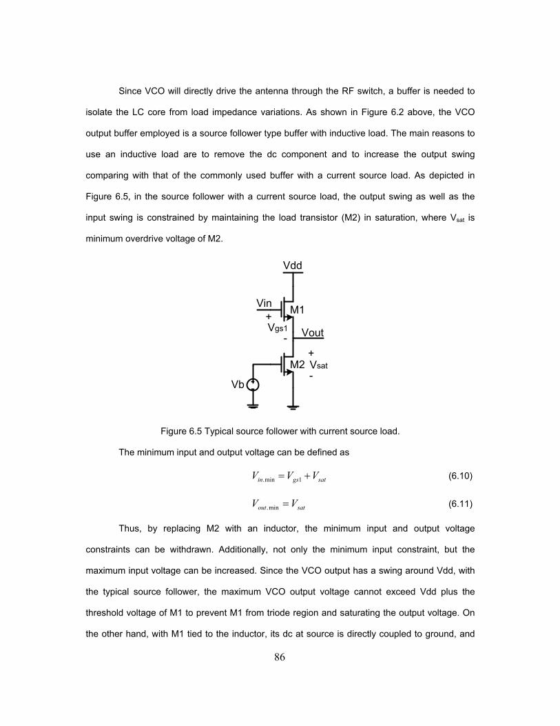
86
Since VCO will directly drive the antenna through the RF switch, a buffer is needed to
isolate the LC core from load impedance variations. As shown in Figure 6.2 above, the VCO
output buffer employed is a source follower type buffer with inductive load. The main reasons to
use an inductive load are to remove the dc component and to increase the output swing
comparing with that of the commonly used buffer with a current source load. As depicted in
Figure 6.5, in the source follower with a current source load, the output swing as well as the
input swing is constrained by maintaining the load transistor (M2) in saturation, where Vsat is
minimum overdrive voltage of M2.
Vb
M2
M1
Vdd
Vin
Vsat
Vgs1
+
-
+
- Vout
Figure 6.5 Typical source follower with current source load.
The minimum input and output voltage can be defined as
satgsin VVV += 1min. (6.10)
satout VV =min. (6.11)
Thus, by replacing M2 with an inductor, the minimum input and output voltage
constraints can be withdrawn. Additionally, not only the minimum input constraint, but the
maximum input voltage can be increased. Since the VCO output has a swing around Vdd, with
the typical source follower, the maximum VCO output voltage cannot exceed Vdd plus the
threshold voltage of M1 to prevent M1 from triode region and saturating the output voltage. On
the other hand, with M1 tied to the inductor, its dc at source is directly coupled to ground, and

87
the drain current of M1 only depends on the buffer input voltage. Thus, the drain current of M1
can have a large range of linear response to the input large signal variation even when M1 is in
triode region especially for the short-channel device, and therefore the larger voltage swing
across the inductor can be obtained from the larger current variations. Note that since the
transistor (M1) employs deep-nwell process, the negative voltage appearing at the source will
not turn on the junction diode between body and source since two can be tied together.
Moreover, without using the extra transistor, the extra noise from the transistor can be avoided.
Figure 6.6 shows the small signal equivalent RLC model of the proposed buffer, where
Cgs and Cgd are ignored and CL represents the load capacitance including all the parasitic
capacitances at output node to ground.
M1
Ls
Vout
CL
Vdd
Ls CL rogmV1
V1+ -
Vin
Vin
Figure 6.6 RLC model of proposed VCO buffer.
The output impedance of this RLC model can be written as
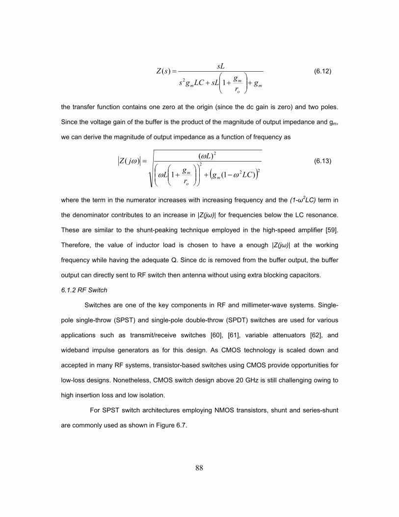
88
mo
mm g
rgsLLCgs
sLsZ+
++
=1
)(2
(6.12)
the transfer function contains one zero at the origin (since the dc gain is zero) and two poles.
Since the voltage gain of the buffer is the product of the magnitude of output impedance and gm,
we can derive the magnitude of output impedance as a function of frequency as
( )22
2
2
)1(1
)()(
LCgrgL
LjZ
mo
m ωω
ωω
−+
+
= (6.13)
where the term in the numerator increases with increasing frequency and the (1-ω2LC) term in
the denominator contributes to an increase in |Z(jω)| for frequencies below the LC resonance.
These are similar to the shunt-peaking technique employed in the high-speed amplifier [59].
Therefore, the value of inductor load is chosen to have a enough |Z(jω)| at the working
frequency while having the adequate Q. Since dc is removed from the buffer output, the buffer
output can directly sent to RF switch then antenna without using extra blocking capacitors.
6.1.2 RF Switch
Switches are one of the key components in RF and millimeter-wave systems. Single-
pole single-throw (SPST) and single-pole double-throw (SPDT) switches are used for various
applications such as transmit/receive switches [60], [61], variable attenuators [62], and
wideband impulse generators as for this design. As CMOS technology is scaled down and
accepted in many RF systems, transistor-based switches using CMOS provide opportunities for
low-loss designs. Nonetheless, CMOS switch design above 20 GHz is still challenging owing to
high insertion loss and low isolation.
For SPST switch architectures employing NMOS transistors, shunt and series-shunt
are commonly used as shown in Figure 6.7.
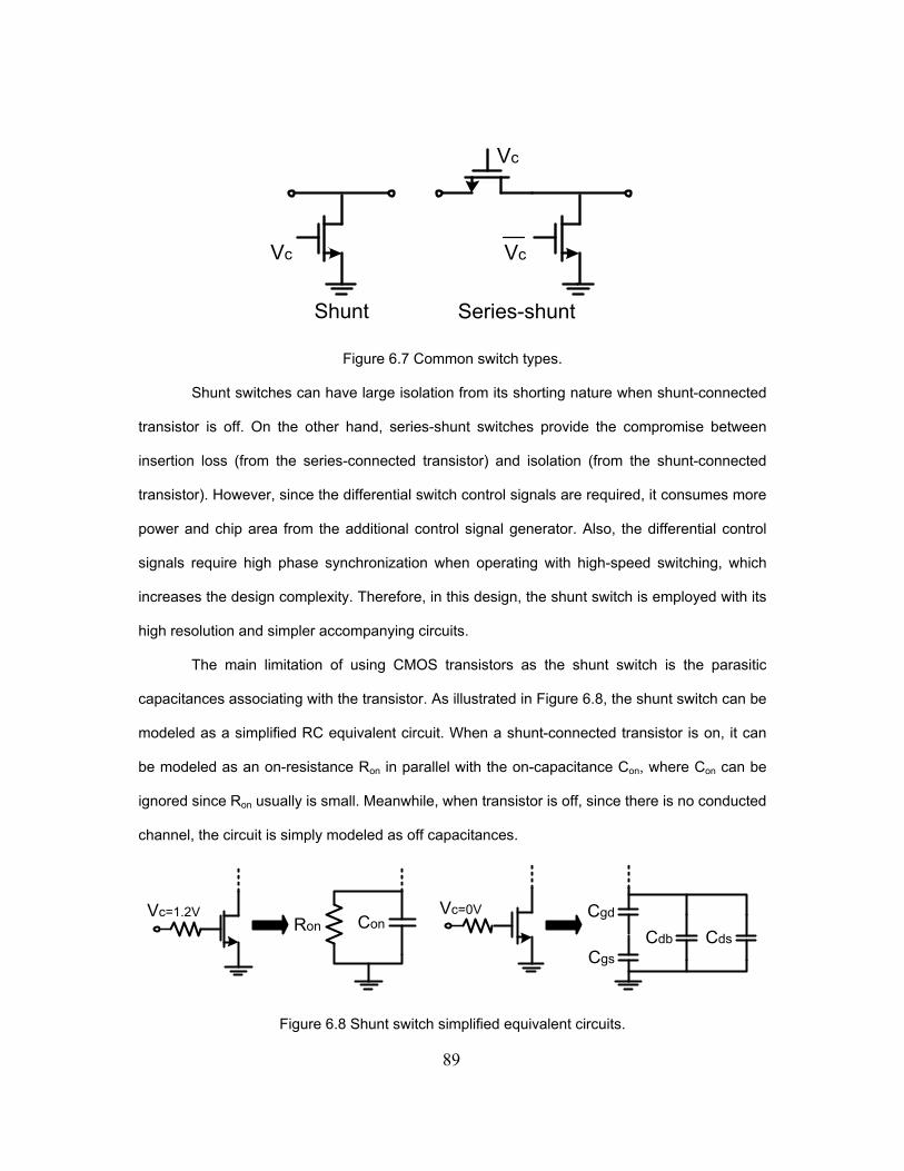
89
Vc
Shunt
Vc
Series-shunt
Vc
Figure 6.7 Common switch types.
Shunt switches can have large isolation from its shorting nature when shunt-connected
transistor is off. On the other hand, series-shunt switches provide the compromise between
insertion loss (from the series-connected transistor) and isolation (from the shunt-connected
transistor). However, since the differential switch control signals are required, it consumes more
power and chip area from the additional control signal generator. Also, the differential control
signals require high phase synchronization when operating with high-speed switching, which
increases the design complexity. Therefore, in this design, the shunt switch is employed with its
high resolution and simpler accompanying circuits.
The main limitation of using CMOS transistors as the shunt switch is the parasitic
capacitances associating with the transistor. As illustrated in Figure 6.8, the shunt switch can be
modeled as a simplified RC equivalent circuit. When a shunt-connected transistor is on, it can
be modeled as an on-resistance Ron in parallel with the on-capacitance Con, where Con can be
ignored since Ron usually is small. Meanwhile, when transistor is off, since there is no conducted
channel, the circuit is simply modeled as off capacitances.
Vc=1.2VConRon
Vc=0V
Cgs
Cgd
Cdb Cds
Figure 6.8 Shunt switch simplified equivalent circuits.
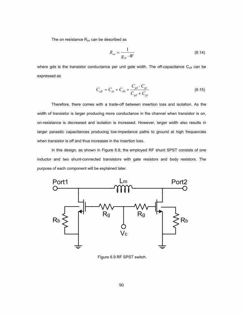
90
The on resistance Ron can be described as
WgR
dson ⋅=
1 (6.14)
where gds is the transistor conductance per unit gate width. The off-capacitance Coff can be
expressed as
gsgd
gsgddbdsoff CC
CCCCC
+⋅
++= (6.15)
Therefore, there comes with a trade-off between insertion loss and isolation. As the
width of transistor is larger producing more conductance in the channel when transistor is on,
on-resistance is decreased and isolation is increased. However, larger width also results in
larger parasitic capacitances producing low-impedance paths to ground at high frequencies
when transistor is off and thus increases in the insertion loss.
In this design, as shown in Figure 6.9, the employed RF shunt SPST consists of one
inductor and two shunt-connected transistors with gate resistors and body resistors. The
purpose of each component will be explained later.
Port1
Rb
Lm
Rg RgRb
Port2
Vc
Figure 6.9 RF SPST switch.

91
As large substrate resistances is usually preferred to float the junction capacitances to
substrate reducing the signal loss [63], in this design, the transistors in the switch employ deep
nwell process for better substrate isolation from its additional PN junction as in [63], [64].
The gate biasing resistors are typically used in RF switch to float the gate at RF so that
the switch power handling performance and linearity can be improved [65]. As illustrated in
Figure 6.10, during the negative cycle of the source signal, when switch is in on-state (transistor
is off), without using the biasing resistor, the transistor will be turned on once the negative
voltage larger than |Vtn|. On the other hand, when gate resistor is applied, the voltage of the
floating gate is mainly determined by the voltage divider from Cgd and Cgs, and thus only
portion of the negative voltage appears at gate allowing larger voltage swing to pass the switch
without distortions. Although large gate resistors are usually preferred to improve isolation at
RF, the resulting large RC time constant at the gate will slow down the transition time of the
input switch control signal. Since for this design the RF switch is used to define the output
impulse pulse width, the value of the gate resistor has to be carefully determined to prevent
larger pulse width than expected.
off off
Figure 6.10 Effect of gate biasing resistor.
As the floating gate affects the power handling performance of the switch, another
reason influencing this performance is from the junction diodes between drain/source and the
substrate. The large negative voltage passing to the switch turns on the junction diode
(especially Cdb for shunt switch) of the transistor limiting the power performance of the switch.

92
To improve this, one way is to use deep-nwell devices to isolate the substrate from drain of the
transistor. However, even with deep-nwell process, the junction diode between drain and body
of the transistor still exists with the same effect on power performance. Therefore, the body-
floating technique is adopted to solve the issue [64]. As shown in Figure 6.9, the body of the
transistors is connected with a resistor to ground. The value of this resistor is usually big to
prevent abrupt current flowing from body when transistor is off and a large negative voltage
passes to the switch. That is, as depicted in Figure 6.11 (a), when transistor is off, it can be
modeled as the Coff with two junction diodes. In Figure 6.11 (b), with body directly connects to
ground, large negative voltage turns on the diode between drain and body resulting large
current since the on-resistance of diode rd is small. When body connects to a large resistor Rb
as in Figure 6.11 (c), the current flowing is reduced by the large resistance in the path. Thus,
the signal loss through the body can be reduced increasing the power handling capability of the
shunt switch.
Coff Coffrd
Coffrd
BodyCd
Rbi
i
(a) (b) (c)
Figure 6.11 Body floating technique [64]: (a) equivalent model of shunt transistors in off-state, (b) without body resistor, (c) with body resistor.
The inductor (Lm) in the RF shunt switch is used to match the transistors’ off-
capacitances (Coff) when switch is in on-state providing a flat frequency response of the
insertion loss. The inductor together with off-capacitance forms a C-L-C π matching network.
Thus, the size of the inductor and transistors are chosen to provide the impedance matching
between the VCO buffer output and load (50 Ω). The minimum length of the transistors is

93
employed to minimize parasitic capacitances while the width is adjusted to have isolation larger
than 30 dB for the switch.
6.1.3 Pulse Generator
The purpose of the pulse generator is to generate the switch control signals
determining the on-off time of the switch and thus defining output impulse pulse width.
Therefore, the generated pulses should have a rail-to-rail output with narrow pulse width (less
than 0.6 ns) producing UWB impulses after the switch. Furthermore, the pulse generator has to
have high driving capability achieving fast rising and falling time for the switch control signals.
Due to the above requirements, the proposed pulse generator is redesigned and
modified from the previously proposed Gaussian pulse generator presented in chapter 5.1.3.
Since the RF shunt switch is in on-state when control signal is “low”, and vice versa, an
inverting output should be generated comparing with the Gaussian pulse generator. Therefore,
instead of using modified XOR gate, the proposed pulse generator has the combination of delay
cell and modified compact XNOR gate as shown Figure 6.12 (a). The delay cell contains
several CMOS inverters (even numbers) in series in order to achieve the required delay (pulse
width) and followed by the last inverter as modified compact XNOR gate.
The gate input of the last inverter (Pn and Nn) is the delayed clock signal while the
original input clock signal is supplied as the Vss (another input) to the last inverter. Output of the
last inverter is “0” only when its Vss is “0” and its input is “1”. Thus, the modified XNOR function
can be formed and generates the required pulse on every falling edge of the input clock signal
as shown in Figure 6.12 (b). The frequency of the input clock signal will determine the PRF of
the output. However, as the same reasons when using modified XOR gate, when the input to
the last inverter and its Vss are both “1” (1.2V), depending on the initial output node voltage, the
output may be either charged only to Vdd-Vtn or floating and susceptible to noise and clock
feedthrough. To avoid the problem, a PMOS (P0) is connected after the last inverter and uses
the output of the first inverter as its gate input to charge the output to “1” when floating. The

94
pulse generator can generate a rail-to-rail output with a fast rising and falling time because of its
simplicity.
(a)
1
2
3
4
t
(b)
Figure 6.12 Proposed pulse generator: (a) schematic, (b) timing diagram.

95
6.1.4 Simulation and Measurement Results of Proposed Impulse Generator
6.1.4.1 Simulation
The proposed UWB impulse generator is fully designed and simulated using TSMC 130
nm CMOS process in Cadence design tool. Figure 6.13 shows the phase noise of VCO with
buffer. The VCO can achieve the phase noise of -105 dBc/Hz at 1 MHz offset, where VCO is
biased at current-limit region with gate of the varactor biased at 1.2 V.
Figure 6.13 Phase noise of VCO with buffer.
As In Figure 6.14, the RF shunt switch has an insertion loss around 2 dB and isolation
higher than 30 dB within the 22-29 GHz band.
Figure 6.14 Insertion loss and isolation of RF shunt switch.

96
In Figure 6.15, from the top to bottom; the input clock signal of the pulse generator,
pulse generator output, and the impulse generator output are shown. Pulse generator generates
the rail-to-rail pulse on every falling edge of the input clock with a PRF of 4 MHz.
Figure 6.15 Simulation of impulse generator.
The close view of the impulse generator output and its PSD are shown in Figure 6.16.
The output has a pulse width of 0.45 ns and a 950 mV peak to peak magnitude. The PSD of the
output has a center frequency of 26 GHz and a -10 dB bandwidth of 4 GHz. Note that the
impulse is generated when VCO is biased at current-limit region with varactor biasing at 1.2 V.
The total power consumption of the impulse generator is 40 mW.

97
(a)
(b)
Figure 6.16 Impulse generator output: (a) transient response, (b) PSD.
When the tail current source is biased at 1.2 V, VCO goes to voltage-limit region. While
varying the biasing the varactor at -2.5 V and 2.5 V, the corresponding impulse generator
outputs and PSDs are shown in Figure 6.17 and Figure 6.18, respectively. The maximum
achievable output swing is 1.14 V. The output spectrum has a center frequency tuning range of
800 MHz from 25.5 GHz to 24.8 GHz. The power consumption is 51 mW.

98
(a)
(b)
Figure 6.17 Impulse generator output with varactor biased at -2.5 V: (a) transient response, (b) PSD.
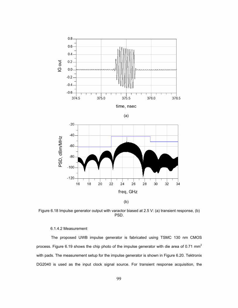
99
(a)
(b)
Figure 6.18 Impulse generator output with varactor biased at 2.5 V: (a) transient response, (b) PSD.
6.1.4.2 Measurement
The proposed UWB impulse generator is fabricated using TSMC 130 nm CMOS
process. Figure 6.19 shows the chip photo of the impulse generator with die area of 0.71 mm2
with pads. The measurement setup for the impulse generator is shown in Figure 6.20. Tektronix
DG2040 is used as the input clock signal source. For transient response acquisition, the

100
oscilloscope Agilent DCA 86100B is employed, while the spectrum analyzer Agilent 8563EC is
used for measuring the PSD.
Figure 6.19 Chip photo of the impulse generator.
DUT
Cascade Microtech Probe Station
Tektronix DG2040
Agilent DCA 86100B
Agilent 8563EC
Clock Generator
Spectrum Analyzer
Oscilloscope
Figure 6.20 Measurement setup.

101
The transient response of the impulse generator output and its PSD are shown in
Figure 6.21 and Figure 6.22, respectively. The measured output pulse width is 0.55 ns with a
swing of 720 mV. Because of the noise level of spectrum analyzer, the output PSD obtained is
with a PRF of 200 MHz to observe the shape of output spectrum. The center frequency is 23.5
GHz. The circuit consumes a DC power of 36 mW. The outputs are obtained from the same
biasing condition as that in the simulation shown in Figure 6.16. Comparing with the simulation
results, the pulse width is slightly increased while the swing is decreased. The center frequency
also shifted down by 2.5 GHz. This is due to the model inaccuracy in the design kit used by the
time of fabrication. The unexpected parasitics degrade the preferable performance of the
impulse generator. Although measurement results are not matched to the simulation results, it
still validates the proposed impulse generator architecture for the UWB automotive radar
application.
Figure 6.21 Measurement of transient impulse generator output.

102
Figure 6.22 Measurement of impulse generator output PSD.
6.2 Differential Carrier-Based UWB Transmitter
In chapter 6.1, since the VCO employed generates differential signals by nature, it is
advantageous to utilize the bi-phase signals with modulation schemes. Therefore, based on the
structures and circuits in the single-ended impulse generator, a differential architecture with bi-
phase modulation is proposed. Bi-phase modulation provides the tolerance of the multi-path
interference [66] and reduces the spectral spikes in the PSD of the transmitting signal [31].
The architecture of the proposed transmitter is shown in Figure 6.23. The design
consists of one VCO, two RF single-pole-single-throw (SPST) switches, one pulse generator,
and one bi-phase modulator. The VCO generates differential outputs with required carrier
frequency. The continuous VCO outputs are then modulated through the RF SPST switches.
The pulse generator generates a train of pulses that controls the RF switches and thus
determines the output pulse-width and the output bandwidth of the switches. The bi-phase
modulator decides either one of the differential switch outputs will pass to antenna by the input
data control signal. All the above components are designed and implemented using TSMC 130
nm CMOS technology with the supply voltage of 1.2 V.

103
Figure 6.23 Block diagram of the proposed transmitter.
6.2.1 VCO
Based on the VCO and buffer presented in chapter 6.1.1, the cross-coupled LC VCO
connects both the differential outputs to output buffers as shown in Figure 6.24. The circuit and
design principles are the same as that for the single-ended VCO in chapter 6.1.1.
Figure 6.24 Schematic of the differential VCO with buffers.

104
6.2.2 RF SPST Switch
The SPST switch used in this design is a shunt switch as for its benefits of high
isolation and simpler associating circuits as mentioned previously. However, from the results of
single-ended impulse generator, it is observed that the finite isolation from the switch
introducing a spectrum spike owing to the carrier leakage. Therefore, to further suppress the
spectrum spike, two cascaded shunt switches are employed in this design to increase the
overall isolation as shown in Figure 6.25. The two cascaded switches form two π matching
networks and thus provide flexibility on choosing inductor and transistors sizes for impedance
matching between VCO and the load at the cost of higher insertion loss and extra chip area.
Figure 6.25 Schematic of the cascaded RF SPST switches.
6.2.3 Pulse Generator
Since the cascaded shunt switches are controlled by the same pulse signals. The same
pulse generator presented in chapter 6.1.3 is employed to achieve the high driving capability to
the switch. Nonetheless, the generated output pulse width is slightly smaller than that of the
previous design to compensate larger RC time constants introduced by cascaded switches at
the gate of the transistors.

105
6.2.4 Bi-Phase Modulator
The schematic of the bi-phase modulator is shown in Figure 6.26. The architecture of
the bi-phase modulator is actually a SPDT switch. The modulator consists of two shunt SPST
switches and output λ/4 matching networks terminating together to the load. The shunt SPDT
switch is chosen in this design since it has the better performance than other switches from its
π-network and λ/4-based architecture especially at higher frequency up to millimeter wave
frequency [63], [67], [68].
The input control signals of the switches are differential and turn on either one of the
switches allowing signal from either port 1 or port 2 to pass to the output. Hence, these control
signals are the input signals for the modulator that provide the modulation data code. The shunt
switches at the first stage of the SPDT switch is designed to have high isolation while providing
the impedance matching between the front SPST switches and the load. However, during the
SPDT operation, when the switch on one side is off, the shunt-connected transistors short the
signals to ground and thus the passing signals on the other side will be directed to this shorting
path instead of the load. Therefore, a λ/4 network can be employed after the switch on both
sides to isolate the shorting path from one another. This concept comes from the λ/4
transmission line. When one end of the λ/4 transmission line is “short”, the “open” is seen at the
other end, and vice versa.
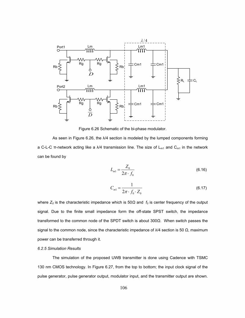
106
Port1
Rb
Lm
Rg RgRb
D
Port2
Rb
Lm
Rg RgRb
D
Cm1
RL CL
Lm1
Lm1
Cm1
Cm1 Cm1
4/λ
Figure 6.26 Schematic of the bi-phase modulator.
As seen in Figure 6.26, the λ/4 section is modeled by the lumped components forming
a C-L-C π-network acting like a λ/4 transmission line. The size of Lm1 and Cm1 in the network
can be found by
0
01 2 f
ZLm ⋅=
π (6.16)
001 2
1Zf
Cm ⋅⋅=
π (6.17)
where Z0 is the characteristic impedance which is 50 Ω and f0 is center frequency of the output
signal. Due to the finite small impedance form the off-state SPST switch, the impedance
transformed to the common node of the SPDT switch is about 300 Ω. When switch passes the
signal to the common node, since the characteristic impedance of λ/4 section is 50 Ω, maximum
power can be transferred through it.
6.2.5 Simulation Results
The simulation of the proposed UWB transmitter is done using Cadence with TSMC
130 nm CMOS technology. In Figure 6.27, from the top to bottom; the input clock signal of the
pulse generator, pulse generator output, modulator input, and the transmitter output are shown.

107
As desired, the frequency of the input clock determines the PRF of the final output and pulse
generator generates the rail-to-rail pulse on every falling edge of the input clock. The transmitter
output has a pulse width about 0.5 ns and has the amplitude of 640 mV when VCO is in the
voltage-limit region. The PRF of 6 MHz is achieved to avoid the ambiguous detection.
Figure 6.27 Transient simulation of the transmitter.
In Figure 6.28, by synchronizing and comparing the two transmitter outputs when
modulator input signal is “1” and “0”, it can be seen that the bi-phase signals are properly
generated. The PSD of the transmitter output is shown in Figure 6.29, which has a center
frequency of 25.2 GHz, a -10 dB bandwidth from 22.9 GHz to 27.6 GHz with the maximum
power spectral density of –54 dBm/MHz, and complies with the FCC requirements. Since the
isolation of the switches is enhanced, carrier leak is diminished and there is no appreciable
single-tone spectral spike in the PSD. The transmitter has a power consumption of 75 mW.

108
Figure 6.28 Comparison of the bi-phase transmitter outputs.
Figure 6.29 PSD of the transmitter out.

109
CHAPTER 7
CONCLUSION
In this dissertation, two impulse generators were proposed for UWB communication
systems and one impulse generator was proposed for UWB automotive radar systems. All the
impulse generators presented were implemented with CMOS technologies overcoming the
design challenges while providing low-cost features. In the first proposed DAC-based impulse
generator for the UWB communication systems, the design can provide high tunabilities varying
output pulse shapes and magnitudes regarding to different PRFs while meeting the FCC mask.
The design can easily adopt OOK and BPM with a novel modulator, which was implemented
and verified from the simulation. The 50 MHz tuning range of PRF was achieved with an output
voltage swing of 335 mV at a 50 MHz PRF and 86 mV at a 100 MHz PRF.
Next, for the UWB communication systems, another filtering-type impulse generator
was proposed. The design composes of a novel and the most compact Gaussian pulse
generator with a compact passive first order BPF. Due to its simplicity, the design has the ultra
low average power consumption of only 0.9 mW at the PRF of 200 MHz. The output of the
impulse generator can be easily modulated with OOK from the feature of modified XOR pulse
generator. The output has a center frequency of 6 GHz, a bandwidth of 9.2 GHz with 50-Ω load
and 6.7 GHz with antenna load. The measured results show great consistencies with the
simulation results.
At last, a new CMOS UWB impulse generator consisting of the VCO, RF switches, and
pulse generator was proposed. The design is fully integrated and designed for 22-29 GHz UWB
automotive radar applications. The design is implemented with single-ended type and
differential architecture with bi-phase modulator. The simulation results show that the proposed
designs complies with the FCC regulations. The PSD of the impulse generator output has a

110
center frequency tuning range of 800 MHz from 25.5 GHz to 24.8 GHz and a -10 dB bandwidth
of 4 GHz providing great range resolution for the UWB radar. Although the measurement results
have a little mismatch with the simulations owing to the model inaccuracy, it still validates the
promises of the proposed design. The proposed impulse generator is power efficient, simplex,
and provides system-on-chip realization.

111
REFERENCES
[1] The Federal Communications Commission, “First Report and Order”, April 2002.
[2] J. Wenger, “Automotive radar - status and perspectives”, Compound IEEE Semiconductor
Integrated Circuit Symposium, CSIC, pp. 4, 30 Oct.-2 Nov. 2005.
[3] M. Schneider, “Automotive Radar- Status and Trends”, In Proc. German Microwave
Conference GeMiC, pp. 144-147, Ulm, Germany, April 2005.
[4] R. J. Fontana and J. F. Larrick, “Waveform adaptive ultra-wideband transmitter,” U.S.
Patent 6026 125, Feb. 15, 2000.
[5] W. Wu, W. Wang, Huarui Yin, and D. Wang, "Carrier-less, single and multi-carrier UWB
radio technology," Ultra Wideband Systems, 2004. Joint with Conference on Ultrawideband
Systems and Technologies. Joint UWBST & IWUWBS. 2004 International Workshop on ,
vol., no., pp. 192- 196, 18-21 May 2004.
[6] V.S. Somayazulu, J. R. Foerster, and S. Roy, "Design challenges for very high data rate
UWB systems," Signals, Systems and Computers, 2002. Conference Record of the Thirty-
Sixth Asilomar Conference on , vol.1, no., pp. 717- 721 vol.1, 3-6 Nov. 2002.
[7] H. Xie, X. Wang, A. Wang, B. Zhao, Y. Zhou, B. Qin, H. Chen, and Z. Wang, “A varying
pulse width 5th-derivative gaussian pulse generator for UWB transceivers in CMOS”, IEEE
Radio and Wireless Symposium, pp. 171 – 174, Jan. 2008.
[8] H. Kim, Y. Joo, and S. Jung, “A Tunable CMOS UWB Pulse Generator”, The 2006 IEEE
2006 International Conference on Ultra-Wideband, pp. 109 – 112, Sept. 2006.
[9] S. Choobkar and A.J. Nabavi, ”A Low Power Programmable CMOS Circuit for Generating
Modulated Pulses for UWB Applications”, The 2nd International Conference on Wireless

112
Broadband and Ultra Wideband Communications, 2007, AusWireless 2007, pp. 5 – 5, Aug.
2007.
[10] S. Bourdel, Y. Bachelet, J. Gaubert, R. Vauche, O. Fourquin, N. Dehaese, and H.
Barthelemy, "A 9-pJ/Pulse 1.42-Vpp OOK CMOS UWB Pulse Generator for the 3.1–10.6-
GHz FCC Band," Microwave Theory and Techniques, IEEE Transactions on , vol.58, no.1,
pp.65-73, Jan. 2010.
[11] J. Lee, Y.-J. Park, M. Kim, C. Yoon, J. Kim, and K.-H. Kim, "System-on-package ultra-
wideband transmitter using CMOS impulse generator," Microwave Theory and Techniques,
IEEE Transactions on, vol.54, no.4, pp. 1667- 1674, June 2006.
[12] M. Demirkan, R. R. Spencer, ”A Pulse-Based Ultra-Wideband Transmitter in 90-nm CMOS
for WPANs”, IEEE Journal of Solid-State Circuits, Volume 43, Issue 12, pp. 2820 – 2828,
Dec. 2008.
[13] Yu-Tso Lin; Hsiao-Chin Chen; Tao Wang; Yo-Sheng Lin; Shey-Shi Lu; , "3–10-GHz Ultra-
Wideband Low-Noise Amplifier Utilizing Miller Effect and Inductive Shunt–Shunt Feedback
Technique," Microwave Theory and Techniques, IEEE Transactions on , vol.55, no.9,
pp.1832-1843, Sep. 2007.
[14] Chung-Yu Wu; Yi-Kai Lo; Min-Chiao Chen; , "A 3–10 GHz CMOS UWB Low-Noise Amplifier
With ESD Protection Circuits," Microwave and Wireless Components Letters, IEEE , vol.19,
no.11, pp.737-739, Nov. 2009.
[15] Reja, M.M.; Moez, K.; Filanovsky, I.; , "An Area-Efficient Multistage 3.0- to 8.5-GHz CMOS
UWB LNA Using Tunable Active Inductors," Circuits and Systems II: Express Briefs, IEEE
Transactions on , vol.57, no.8, pp.587-591, Aug. 2010.
[16] Jeong-Bae Seo; Jong-Ha Kim; Hyuk Sun; Tae-Yeoul Yun; , "A Low-Power and High-Gain
Mixer for UWB Systems," Microwave and Wireless Components Letters, IEEE , vol.18,
no.12, pp.803-805, Dec. 2008

113
[17] Pei-Zong Rao; Tang-Yuan Chang; Ching-Piao Liang; Shyh-Jong Chung; , "An Ultra-
Wideband High-Linearity CMOS Mixer With New Wideband Active Baluns," Microwave
Theory and Techniques, IEEE Transactions on , vol.57, no.9, pp.2184-2192, Sept. 2009.
[18] Jouri, M.; Golmakani, A.; Yahyabadi, M.; Khosrowjerdi, H.; , "Design and simulation of a
down-conversion CMOS mixer for UWB applications," Electrical Engineering/Electronics
Computer Telecommunications and Information Technology (ECTI-CON), 2010
International Conference on , vol., no., pp.937-940, 19-21 May 2010
[19] Makarov, D.G.; Krizhanovskii, V.V.; Chang Shu; Krizhanovskii, V.G.; , "CMOS 0.18-μm
integrated power amplifier for UWB systems," Ultrawideband and Ultrashort Impulse
Signals, 2008. UWBUSIS 2008. 4th International Conference on , vol., no., pp.153-155, 15-
19 Sept. 2008
[20] Sew-Kin Wong; Maisurah, S.; Osman, M.N.; Kung, F.; Jin-Hui See; , "High efficiency CMOS
power amplifier for 3 to 5 GHz ultra-wideband (UWB) application," Consumer Electronics,
IEEE Transactions on , vol.55, no.3, pp.1546-1550, August 2009.
[21] A. Oncu, B. B. M. W. Badalawa, and M. Fujishima, ”22–29 GHz Ultra-Wideband CMOS
Pulse Generator for Short-Range Radar Applications”, IEEE Journal of Solid-State Circuits,
Volume 42, Issue 7, pp.1464 – 1471, July 2007.
[22] H. Krishnaswamy, H. Hashemi, “A 4-Channel 24-27 GHz UWB Phased Array Transmitter in
0.13um CMOS for Vehicular Radar”, IEEE Custom Integrated Circuits Conference, CICC.
pp. 753 – 756, Sept. 2007.
[23] J. Wernehag, and H. Sjoland, "A 24-GHz Automotive Radar Transmitter with Digital Beam
Steering in 130-nm CMOS," Research in Microelectronics and Electronics 2006, Ph. D.,
vol., no., pp.481-484, 0-0 0.
[24] http://edocket.access.gpo.gov/cfr_2002/octqtr/pdf/47cfr15.209.pdf

114
[25] C. E. Shannon, R. G. Gallager, and E. R. Berlekamp, “Lower bounds to error probability for
coding on discrete memoryless channels,” Infor. And Control,vol. 10, 1967, pp.65-103 (Part
I), pp. 522-552 (Part II).
[26] Welborn, M.; McCorkle, J.; , "The importance of fractional bandwidth in ultra-wideband
pulse design," Communications, 2002. ICC 2002. IEEE International Conference on , vol.2,
no., pp. 753- 757 vol.2, 2002.
[27] Hongsan Sheng; Orlik, P.; Haimovich, A.M.; Cimini, L.J., Jr.; Jinyun Zhang; , "On the
spectral and power requirements for ultra-wideband transmission," Communications, 2003.
ICC '03. IEEE International Conference on , vol.1, no., pp. 738- 742 vol.1, 11-15 May 2003.
[28] M. Di Benedetto, G. Giancola, Understanding Ultra Wide Band Radio Fundamentals,
Prentice Hall, 2004.
[29] D. Baranauskas and D. Zelenin, "A 0.36W 6b up to 20GS/s DAC for UWB Wave
Formation," Solid-State Circuits Conference, 2006. ISSCC 2006. Digest of Technical
Papers. IEEE International , vol., no., pp.2380-2389, 6-9 Feb. 2006.
[30] A. Jha, R. Gharpurey, and P. Kinget, "Quadrature-DAC based pulse generation for UWB
pulse radio transceivers," Circuits and Systems, 2006. ISCAS 2006. Proceedings. 2006
IEEE International Symposium on , vol., no., pp.4 pp., 0-0 0, 2006.
[31] Veenstra, H.; van der Heijden, E.; van Goor, D.; , "15-27 GHz pseudo-noise UWB
transmitter for short-range automotive radar in a production SiGe technology," Solid-State
Circuits Conference, 2005. ESSCIRC 2005. Proceedings of the 31st European , vol., no.,
pp. 275- 278, 12-16 Sept. 2005.
[32] Fukuda, T.; Negoro, N.; Ujita, S.; Nagai, S.; Nishijima, M.; Sakai, H.; Tanaka, T.; Ueda, D.; ,
"A 26GHz Short-Range UWB Vehicular-Radar Using 2.5Gcps Spread Spectrum
Modulation," Microwave Symposium, 2007. IEEE/MTT-S International , vol., no., pp.1311-
1314, 3-8 June 2007.

115
[33] C. Shu; M.S. Kang; S.K. Han, and S.G. Lee, "A single chip CMOS transmitter for UWB
impulse radar applications," Microwave Conference, 2008. APMC 2008. Asia-Pacific , vol.,
no., pp.1-4, 16-20 Dec. 2008.
[34] V. Cojocaru, H. Kurata, D. Humphrey, B. Clarke, T. Yokoyama, V. Napijalo, T. Young, and
T. Adachi, "A 24GHz Low-Cost, Long-Range, Narrow-Band, Monopulse Radar Front End
System for Automotive ACC Applications," Microwave Symposium, 2007. IEEE/MTT-S
International , vol., no., pp.1327-1330, 3-8 June 2007.
[35] R. Xu, Y. Jin, and C. Nguyen, "Power-efficient switching-based CMOS UWB transmitters for
UWB communications and Radar systems," Microwave Theory and Techniques, IEEE
Transactions on , vol.54, no.8, pp.3271-3277, Aug. 2006.
[36] Gresham, I.; Jenkins, A.; Egri, R.; Eswarappa, C.; Kinayman, N.; Jain, N.; Anderson, R.;
Kolak, F.; Wohlert, R.; Bawell, S.P.; Bennett, J.; Lanteri, J.-P.; , "Ultra-wideband radar
sensors for short-range vehicular applications," Microwave Theory and Techniques, IEEE
Transactions on , vol.52, no.9, pp. 2105- 2122, Sept. 2004.
[37] M. Ghavami, L. B. Michael, and R. Kohno, Ultra wideband, signal and systems in
communication engineering, 2004.
[38] M. L. Welborn, “System considerations for ultra-wideband wireless networks,” in IEEE
Radio and Wireless conf., Boston, MA, August 19-22, 2001, pp. 5-8.
[39] J. W. McCorkle, Ultra wideband communication system, method, and device with low noise
pulse formation, U.S. Patent 6735238, May 11, 2004.
[40] J. G. Proakis, Digital Communications. New York: McGraw-Hill, 3rd ed., 1995.
[41] H. Kim, D. Park, and Y. Joo, "Design of CMOS Scholtz's monocycle pulse generator," Ultra
Wideband Systems and Technologies, 2003 IEEE Conference on , vol., no., pp. 81- 85, 16-
19 Nov. 2003.

116
[42] Y. Zhu; J.D. Zuegel, J.R. Marciante, and H. Wu, "Distributed Waveform Generator: A New
Circuit Technique for Ultra-Wideband Pulse Generation, Shaping and Modulation," Solid-
State Circuits, IEEE Journal of, vol.44, no.3, pp.808-823, Mar. 2009.
[43] B. Ravazi, Principles of Data Conversion System Design. New York: Willey, 1995.
[44] J. Martin, Analog Integrated Circuit Design: Willey, 1997.
[45] Y. Jeong, S. Jung, and J. Liu, A CMOS impulse generator for UWB wireless communication
systems, International Symposium on Circuits and Systems, pp. 129-132, May 2004.
[46] J. P. Uyemura, CMOS Logic Circuit Design:Kluwer Academic Publishers, 2001.
[47] S. Winder, Analog and Digital Filter Design, Newnes, 2002.
[48] F. Demeestere, C. Delaveaud, and J. Keignart, "A compact UWB antenna with a wide band
circuit model and a time domain characterization," Ultra-Wideband, The 2006 IEEE 2006
International Conference on , vol., no., pp.345-350, 24-27 Sept. 2006.
[49] B. Jung, Y. Tseng, J. Harvey, and R. Harjani, ”Pulse generator design for UWB IR
communication systems” IEEE International Symposium on Circuits and Systems, ISCAS,
pp. 4381- 4384 Vol. 5, May 2005.
[50] Y. Wang, S. M. Kilambi, K. Iniewski, and V. Gaudet, ”A fully integrated CMOS transmitter
design for IR-UWB communication systems”, Midwest Symposium on Circuits and Systems,
MWSCAS, pp. 738 – 741, Aug. 2007.
[51] M. I. Skolnik, Introduction to Radar Systems: McGraw-Hill, 2003.
[52] P. Sameni,C. Siu, S. Mirabbasi, H. Djahanshahi, M. Hamour, K. Iniewski, and J. Chana
“Modeling and Characterization of VCOs with MOS Varactors for RF Transceivers”
EURASIP Journal on Wireless Communications and Networking, Volume, Issue 2, pp. 1–
12, 2006.
[53] O. T. Ogunnika “A Simple Transformer-Based Resonator Architecture for Low Phase Noise
LC Oscillators” Theses, MIT, 2004.

117
[54] B. Ravazi, Designof Analpg CMOS Integrated Circuits: McGraw-Hill, 2002.
[55] N.M. Nquyen and R.G. Meyer, “Start-up and Frequency Stability in High-Frequency
Oscillators,” IEEE Journal of Solid-State Circuits, vol. 27, pp. 810-829, May 1992.
[56] R. G. Meyer, “Advanced integrated circuits for communications,” EECS 242 Class Notes,
University of California, Berkeley, 1998.
[57] P. Andreani and S. Mattisson, “On the use of MOS varactors in RF VCOs,” IEEE Journal of
Solid-State Circuits, vol. 35, no. 6, pp. 905–910, 2000.
[58] A. Hajimiri and T. H. Lee, “Design issues in CMOS differential LC oscillators,”IEEE Journal
of Solid-State Circuits, vol. 34, no. 5, pp. 717–724, May 1999.
[59] T. H. LEE, The Design of CMOS Radio-Frequency Integrated Circuits: Cambridge, 2004.
[60] Z. Li, H. Yoon, F.-J. Huang, and K. K. O, “5.8 GHz CMOS T/R switches with high and low
substrate resistances in a 0.18 um CMOS process,” IEEE Microw. Wireless Compon. Lett.,
vol. 13, no. 1, pp. 1–3, Jan. 2003.
[61] N. A. Talwalkar, C. P. Yue, H. Gan, and S. S.Wong, “Integrated CMOS transmit-receive
switch using LC-tuned substrate bias for 2.4 GHz and 5.2 GHz applications,” IEEE J. Solid-
State Circuits, vol. 39, no. 6, pp. 863–870, Jun. 2004.
[62] A. Tomkins, P. Garcia, and S. P. Voinigescu, "A 94GHz SPST Switch in 65nm Bulk CMOS,"
Compound Semiconductor Integrated Circuits Symposium, 2008. CSIC '08. IEEE , vol., no.,
pp.1-4, 12-15 Oct. 2008.
[63] B.-W. Min and G. M. Rebeiz, "Ka-Band Low-Loss and High-Isolation Switch Design in 0.13-
um CMOS," Microwave Theory and Techniques, IEEE Transactions on , vol.56, no.6,
pp.1364-1371, June 2008.
[64] M.-C. Yeh, Z.-M. Tsai, R.-C. Liu, K.-Y. Lin, Y.-T. Chang and H. Wang, "Design and analysis
for a miniature CMOS SPDT switch using body-floating technique to improve power
118
performance," Microwave Theory and Techniques, IEEE Transactions on , vol.54, no.1, pp.
31- 39, Jan. 2006.
[65] C. Tinella, J. M. Fournier, D. Belot, and V. Knopik, "A high-performance CMOS-SOI
antenna switch for the 2.5-5-GHz band," Solid-State Circuits, IEEE Journal of , vol.38, no.7,
pp. 1279- 1283, July 2003.
[66] Y. Kawano, Y. Nakasha, T. Suzuki, T. Ohki, T. Takahashi, K. Makiyama, T. Hirose, and K.
Joshin, "Sub-10 ps Pulse Generator with Biphase Modulation Function in 0.13-um InP
HEMT," Radar Conference, 2006. EuRAD 2006. 3rd European , vol., no., pp.342-345, 13-
15 Sept. 2006
[67] K.-Y. Lin, W.-H. Tu, P.-Y. Chen, H.-Y. Chang, H. Wang, and R.-B. Wu, "Millimeter-wave
MMIC passive HEMT switches using traveling-wave concept," Microwave Theory and
Techniques, IEEE Transactions on , vol.52, no.8, pp. 1798- 1808, Aug. 2004.
[68] M. Uzunkol, and G. M. Rebeiz, "A Low-Loss 50–70 GHz SPDT Switch in 90 nm CMOS,"
Solid-State Circuits, IEEE Journal of , vol.45, no.10, pp.2003-2007, Oct. 2010.

119
BIOGRAPHICAL INFORMATION
Ju-Ching Li was born in Taipei, Taiwan. He graduated from TamKang University,
Taiwan with his Bachelor’s degree in Mechanical Engineering in 2001. He received his Master’s
degree in Electrical Engineering from the University of Texas at Arlington in 2005. He joined the
Analog and Mixed signal IC design lab and worked toward his PhD degree under Dr. Sungyong
Jung at the University of Texas at Arlington from 2006. His research interests include analog,
mixed-signal, and RF integrated circuit design especially for the Ultra-Wideband (UWB)
communication and radar systems.


![Code No: HIGH VOLTAGE ENGINEERING - padhle.com · impulse generator circuits. [7] 5 a) ... Explain about tripping and control of impulse generators. [7] 5 a) With neat sketch,](https://img.dokumen.tips/doc/110x75/5b55ff9d7f8b9ad9688c03ab/code-no-high-voltage-engineering-impulse-generator-circuits-7-5-a-.jpg)