Embed Size (px)
Citation preview

D~5C-c::t\ +~VI u ~ -,. ANALOGW DEVICES
+5VPoweredCMOSRS-232Drivers/Receivers
FEATURESSingle 5 V Power SupplyMeets All RS-232-C and V.28 SpecificationsMultiple Drivers and ReceiversOn-Board DC-DC Converters:t:9 V Output Swing with +5 V Supplylow Power CMOS: 5 mA Operationlow Power Shutdown $1 p.A3-State TTl/CMOS Receiver Outputs:t:30 V Receiver Input levelsPlug-In Replacement for MAX230-241
APPLICATIONSComputersPeripheralsModemsPrintersInstruments
GENERAL DESCRIPTIONThe AD230 family of 5 V only, RS-232 line drivers/receiversprovides a variety of configurations to fit most communicationneeds, especially in applications where :t 12 V is not available.The AD230, AD235, AD236 and AD241 feature a low powershutdown mode which reduces power dissipation to less than5 j.LW making them ideally suited for battery powered equip-ment. The AD233 and AD235 do not require any external com-ponents and are particularly useful in applications where printedcircuit board space is critical.
1\ll members of the AD230 family, except the AD231 and theAD239, include tWointernal charge pump voltage converterswhich allow operation from a single +5 V supply. These con-verters convert the + 5 V input power to the :t 10 V required forRS-232 output levels. The AD231 and AD239 are designed tooperate from +5 V and + 12 V supplies. An internal + 12 V to- 12 V charge pump voltage converter generates the - 12 Vsupply.
In order to minimize the package count in all applications, awide selection of driver/receiver combinations is available (seetable below).
SELECTION TABLE
Information furnished by Analog Devices is believed to be accurate andreliable. However, no responsibility is assumed by Analog Devices for itsuse; nor for any infringements of patents or other rights of third partieswhich may result from its use. No license is granted by implication orotherwise under any patent or patent rights of Analog Devices.
"
One Technology Way, P.O. Box 9106, Norwood, MA 02062-9106, U.S.A.Tel: 617/329-4700 Fax: 617/326-8703 Twx: 710/394-6577Telex: 924491 Cable: ANALOG NORWOODMASS
No. of No. of Low Power TTLPart Power RS-232 RS-232 External Shutdown Three-State No. ofNumber Supply Voltage Drivers Receivers Capacitors (SD) EN Pins
AD230 +5 V 5 0 4 Yes No 20AD231 +5 V & +7.5 V 2 2 2 No No 14
to 13.2VAD232 +5 V 2 2 4 No No 16AD233 +5 V 2 2 None No No 20AD234 +5 V 4 0 4 No No 16AD235 +5 V 5 5 None Yes Yes 24AD236 +5 V 4 3 4 Yes Yes 24AD237 +5 V 5 3 4 No No 24AD238 +5 V 4 4 4 No No 24AD239 +5 V & +12 V 3 5 2 No Yes 24AD241 +5 V 4 5 4 Yes Yes 28
OBSOLETE

SPECIFICATIONS(Vee = +5 V:t 10% (AD231,AD232,AD234,AD236,AD238,AD239,AD241);Vee= +5 V :t 5% (AD233,AD235);V+ = 7.5Vto 13.2V (AD231)&V+ = 12 V :t 10% (AD239);All Specifications Tminto Tmaxunlessotherwisenoted.)
NOTE'Sample tested to ensure compliance.
Specifications subject to change without notice.
ABSOLUTE MAXIMUM RATINGS*(T A = 25°C unless otherwise noted)
Vcc 0.3Vto+6V
V+ (Vcc-0.3V)to+13VV- +0.3Vto-13VInput Voltages
TIN 0.3Vto(Vcc+0.3V)R1N ::I::30V
Output Voltages
TOUT' . . . . . . . . . . . . . . (V+, +0.3 V) to (V-, -0.3 V)ROUT O.3Vto(Vcc+O.3V)
Short Circuit Duration
TOUT Continuous
Power DissipationCerdip (Derate 9.5 mW/OCabove +70°C) 675 mWPlastic DIP (Derate 7 mW/OCabove +70°C) 375 mWSOIC (Derate 7 mW/oC above +70°C) 375 mW
Operating Temperature RangeCommercial (J Version) 0 to +70°CIndustrial (A Version) . . . . . . . . . . . . . . . -40°C to +85°CExtended (S Version) """"""" -55°C to + 125ac
Storage Temperature Range. . . . . . . . . . . -65ac to + 150acLead Temperature (Soldering, 10 secs) . . . . . . . . . . . + 300°C
*This is a stress rating only and functional operation of the deviceat these or any other conditions above those indicated in theoperation sections of this specification is not implied. Exposureto absolute maximum rating conditions for extended periods oftime may affect reliability.
CAUTION
ESD (electrostatic discharge) sensitive device. The digital control inputs are diode protected;however, permanent damage may occur on unconnected devices subject to high energy electro-static fields. Unused devices must be stored in conductive foam or shunts. The protective foamshould be discharged to the destination socket before devices are removed.
-2-
~--- -
Parameter Min Typ Max Units Test Conditions/Comments
Output Voltage Swing ::I::5 ::I::9 Volts All Transmitter Outputs Loaded with 3 kil to GroundVcc Power Supply Current 4 10 mA No Load, T A = 25°C
0.4 1 mA AD231, AD239V+ Power Supply Current 5 10 mA No Load, V+ = 12 V AD231 & AD239 OnlyShutdown Supply Current 1 10 f.LA TA = +25°CInput Logic Threshold Low, VINL 0.8 V TIN' EN, SDInput Logic Threshold High, VINH 2.0 V TIN' EN, SDLogic Pullup Current 15 200 f.LA TIN = 0 VRS-232 Input Voltage Range -30 +30 VRS-232 Input Threshold Low 0.8 1.2 V Vcc = 5 V, TA = +25°CRS-232 Input Threshold High 1.7 2.4 V Vcc = 5 V, TA = +25°CRS-232 Input Hysteresis 0.2 0.5 1.0 V Vcc=5VRS-232 Input Resistance 3 5 7 kil Vcc = 5V, TA = +25°CTTL/CMOS Output Voltage Low, VOL 0.4 V lOUT = 3.2 mATTL/CMOS Output Voltage High, VOH 3.5 V lOUT = -1.0 mATTL/CMOS Output Leakage Current 0.05 ::1::10 f.LA EN = Vceo0 V ::; ROUT::;VccOutput Enable Time (TEN) 400 ns AD235, AD236, AD239, AD241
(Figure 25. RL = 1 kil, CL = 150 pF)Output Disable Time (Tod 250 ns AD235, AD236, AD239, AD241
(Figure 25. RL = 1 kil, CL = 150 pF)Propagation Delay 0.5 f.Ls RS-232 to TTLInstantaneous Slew Ratel 30 V/f.LS CL = 10pF, RL = 3-7kil, TA = +25°CTransition Region Slew Rate 3 V/f.LS RL = 3 kil, CL = 2500pF
Measured from +3 V to -3 V or -3 V to +3 VOutput Resistance 300 il Vcc = V+ = V- = 0 V, VOUT= ::1::2VRS-232 Output Short Circuit Current ::1::10 mA
OBSOLETE

)
)
)
)
)
T30UT
T10UT
T20UT
T21N
T1IN AD230TOP VIEW
(Not to Scale)GND
Vcc
C1+
V+
NC =NO CONNECT
Figure 1. AD230 DIP/SOIC Pin ConfigurationGND-
6-"INTERNAL 400kfl PULL.UP RESISTORON EACH TTLiCMOS INPUT
Figure 2. AD230 Typical Operating Circuit
DIP
AD231TOP VIEW
(Not to Scale)T10UT
A1oUT
T21N T11N
SOIC
.C+C-V-
T20UT
A21N
AD231TOP VIEW
(Not to Scale) II!!!A11N
A2oUT
T21N
NC
NC =NO CONNECT
Figure 3. AD231 DIP & SOIC Pin Configurations
{
T11NTTLICMOSINPUTS*
T21N
{
R10UT
TTL/CMOSOUTPUTS
R2oUT
AD231GND-
12-"INTERNAL 400kfl PULL.UP RESISTORON EACH TTL/CMOS INPUT
**INTERNAL 5kfl PULL.DOWN RESISTORON EACH RS.232 INPUT
Figure 4. AD231 Typical Operating Circuit
-3-
10l-lF
I+ 16V
T1INT 12 . T1oUT
T21N4 3
T2oUT
TTL/CMOS i T31N14 1 2"
INPUTS* T30UT OUTPUTS
15 20T41N T4oUT
T5'N19 16
T50UT,
NC18
AD23017
SD
1N914 OR EQUIVALENTVcc I..T
C+ V++12V TO -12V
VOLTAGECONVERTERv-h4.71-lF
C- I+16V
81 1_'-...- 111
. T1. }
RS-232OUTPUTS
71 I_- 14 . T2oUT
91 _"""':-1 110
RI'"}
.RS-232
_./ I 15INPUTS**
61R21N
OBSOLETE

AD232TOP VIEW
(Not to Scale)
Figure 5. AD232 DIP/SOIC Pin Configuration
+5VINPUT
10".F...L+6.3VI
161 '(;1+ Vcc
+5V TO +10V 23Ic1-VOLTAGE DOUBLERV+
641C2+ +10V TO -10V V-
C2-VOLTAGEINVERTER5
10".F
~+16:0"'
}RS-232OUTPUTS
T2oUT
R1'N
}RS-232INPUTS"
R2'N
-'INTERNAL 400kil PULL-UP RESISTORON EACH TTLiCMOS INPUT
**INTERNAL 5kil PULL-DOWN RESISTORON EACH RS-232 INPUT
+5VINPUT
7
Vcc
{n'N
TTL/CMOSINPUTS'
T2'N
C2+
~
11
C2+ 15
C2- 10
AD232GND-
15
Figure 6. AD232 Typical Operating Circuit
T21N
T11N
R1oUT
R11N
T1oUT AD233TOPVIEW
(Not to Scale)GND
VCC
C1+
GND
Figure 7. AD233 DIP Pin Configuration
2
{R10UT
TTL/CMOSOUTPUTS
R2oUT -
DO NOT MAKE
{CONNECTIONS TOTHESE PINS
INTERNAL
{-10V POWERSUPPLY
INTERNAL+10V POWERSUPPLY
3
20
8C1+
~C1-
121V- AD23317
V-C2- .16
14. V+2,ND
6~
9
-'INTERNAL 4O0kil PULL-UP RESISTORON EACH TTLiCMOS INPUT
"INTERNAL 5kil PULL-DOWN RESISTORON EACH RS-232 INPUT
Figure 8. AD233 Typical Operating Circuit
-4-~- ---
5T1oUT
}
RS-232OUTPUTS
T2oUT
R1'N
}RS-232INPUTS"
R2'N
18
4
19
{ T1,"1
1_"'- 114
TTL/CMOSINPUTS'
T2'N11_"'- 17
{ RI, I
_/.I 113
TTL/CMOSOUTPUTS
R2oUT- 91 __I 18OBSOLETE

J+5VINPUT
Vcc
7. VC1+ cc+5V TO +10V 8
9Ic1-VOLTAGE DOUBLERV+12
101C2+ +10V TO -10V V-C2-VOLTAGE INVERTER
6
10l1F
~+16V
T10UT
T2oUT
V+ C1-
T21N
T11NAD234
TOP VIEW(Not to Scale)GND
C1+
)Figure 9. AD234 DIP/SOIC Pin Configuration AD234
GND~-
'INTERNAL 400kfi PULL-UP RESISTORON EACH TTL/CMOS INPUT
Figure 10. AD234 Typical Operating Circuit
) +5VINPUT
12
v:T1'N 8 3 T10UT
T20N 7 4 T2oUT
TIL/CMOS ~ 15 2 I RS-232
INPUTS' I T3'N T30UT r OUTPUTS
T~: :~ ~T~15'N 15 15ouTAD235
R1ouT 9 10 R1'N
R2oUT 6 5 R2'N
TIL/CMOS I 23 24 ~RS-232
OUTPUTS 1 R3oUT R3'N I INPUTS"
R4oUT 17 18 R4.N
14 13R5oUT R5'N
- ~ ~EN SD
GND
~11'INTERNAL4OOkU PUll-UP RESISTOR ON EACH TTlfCMOS INPUT
"INTERNAl SkU PUll-DOWN RESISTOR ON EACH RS-232 INPUT
Figure 12. AD235 Typical Operating Circuit
-5-
Figure 11. AD235 DIP Pin Configuration
)
T1'N4
T10UT
T2'N3 2
T20UT
TTL/CMOS i RS-232INPUTS* OUTPUTS
T3'N13 16
T30UT
T4'N . 141 I P5 .T40UT
T4oUT
T30UT
T10UT
\ ) T2OUT
R21N
R2 AD235TOP VIEW
T21N 7 (Not to Scale)
T1IN
R1oUT
OBSOLETE

Figure 13. AD236 DIP/SOIC Pin Configuration
10".F10 ~ T-
6.3VC1+ Vcc +
121C1- vo~i:G~OD~0°~lER V+ 11
131C2+ +10VTO-10V V- 15C2- VOLTAGE INVERTER
14 -
T30UT
T1oUT
T2oUT
R11N
R1oUT
T21N AD237TOP VIEW
(Not to Scale)T11N
GND
Vcc
Figure 15. AD237 DIP/SOIC Pin Configuration
GND-8
-='INTERNAl400kU PUll-UP RESISTOR ON EACH TTl/CMOS INPU-;
ulNTERNAl 5kU PUll-DOWN RESISTOR ON EACH RS-232 INPUT
10".F
J::+16V
2
3
-6-
Figure 16. AD237 Typical Operating Circuit
10".F
*+16V
T1'N2
T10UT
T2'N6 3
T2ouT
TTL/CMOS 1RS-232
INPUTS' OUTPUTS18 1
TJON T30uT
AD23619 24
T4'N T4 T4oUT
5 4R1oUT R1 R1'N
TTL/CMOS122 23
I RS-232
OUTPUTS R2oUT R2'N INPUTS'
R30UT17 16
R30N
EN20 21
SDGND
-4-8
'INTERNAL400kH PUll.UP RESISTORON EACHTTl/CMOS INPUTuiNTERNAl5kH PUll.DOWN RESISTORON EACHRS.232 INPUT
Figure 14. AD236 Typical Operating Circuit
T30UT 11 I .
T10UT
T2oUT
R1'N
R1oUT
T2"; AD235TOP VIEW
T11N 7 (Notto Scale)GND
Vcc
7T1'N-
6T2'N-
TTLICMOSi18
TJON-INPUTS'
19T4'N-
21T5'N-
R1oUT..--2.
22
TTLICMOS iR2oUT-
OUTPUTS
17R30UT
AD23724
20
4
23
16
T10UT
"-. "'.,'T30UT OUTPUTS
T4ouT
T50UT
:
R1'N
"mR2oN INPUTS"
R:lIN
OBSOLETE

AD238TOP VIEW
(Not to Scale)
10f.'F
*+16V
}
R11N
2T10UT
T2oUT
nOUT
R2'N
R2oUT
n'N
R1oUT24
AD23820
GND
Vcc
) 23
16
Figure 17, AD238 DIP/SOIC Pin ConfigurationGND---e=
'INTERNAL 400k1l PUll.UP RESISTOR ON EACH TTliCMOS INPUT"INTERNAl 5k1l PUll-DOWN RESISTOR ON EACH RS.232 INPUT
) Figure 18. AD238 Typical Operating Circuit
NC= NO CONNECT
) Figure 19. AD239 DIP/SOIC Pin Configuration
GND~=
'INTERNAL 400k1l PUll.UP RESISTOR ON EACH Tn/CMOS INPUT"INTERNAl 5kll PUll.DOWN RESISTOR ON EACH RS.232 INPUT
Figure 20, AD239 Typical Operating Circuit
-7-
T20UTRS-232OUTPUTS
IT30UT
T4ouT
R1'N
R2'N,
RS-232INPUTS"
,R3'N
R4'N
+12V:10%
1N914OREQUIVALENT
10f.'F
{'
n'N n nOUT
TTL/CMOS 23 20 RS-232INPUTS. T2'NT20UT OUTPUT!>
--;--4TJ'N T3 T30UTAD239
R1oUT. "I O<.R1R1'N
22 21R2oUT R2'N
TTLiCMOS J 17 18
IRS-232
OUTPUTS R30UT R3'N INPUTS"
R4oUT11 12
R4'N
R50u,10 9
R5'N
EN14 15
NC
R1oUT
)R1'N
GND
VCC
V+
C+ AD239TOP VIEW
(Not to Scale)V-
R5'N
OBSOLETE

12 .C1+ Vcc
I +5V TO +10V 1314 C1- VOLTAGE DOUBLERV+
17151C2+ +10V TO -10V V- 10",F
VOLTAGE INVERTERI
16VC2- +
16 -= ,n'N 7 2 nOUT
T2'N 6 3 T2oUT~~~ I~INPUTS' I r OUTPUTS
T3'N 20 1 T30uT
~~T4'N~- ITy I - T4oUT
AD2418 9
R1oUT R1'N
R2oUT 5 4 R2'N
TTL/CMOS -1 26 27 L RS-232
OUTPUTS I R30UT R3'N r INPUTS"
R4oUT 22 23 R4'N
R50UT 19 18 R5'N
- 24 25EN SD
GND
-4:- 10'INTERNAL400kU PUll-UP RESISTORON EACHTTl/CMOSINPUT
ulNTERNAl SkU PUll-DOWN RESISTORON EACHRS-232INPUT
Figure 22. AD241 Typical Operating Circuit
Figure 21. AD241 SOIC Pin Configuration
-8-
T30UT I1 I.
nOUT
T2OUT
R21N
R2oUT
T21NAD241
T11N 7 TOP VIEW
R1oUT B (NottoScale)
R11NOBSOLETE

')
PIN FUNCTIONDESCRIPTION
Mnemonic Function
Vcc Power Supply Input 5 V :!: 10% (AD231, AD232, AD234, AD236, AD238, AD239, AD241).5 V:!: 5% (AD233, AD235).
Internally generated positive supply (+ 10 V nominal) on all parts except AD231 and AD239.AD231 requires external 7.5 V to 13.2 V supply; AD239 requires external 10.8 V to 13.2 V supply.
V+
V-
GND
Internally generated negative supply (-10 V nominal).
Ground pin. Must be connected to 0 V.
C+
C-
(AD231 and AD239 only). External capacitor (+ terminal) is connected to this pin.
(AD231 and AD239 only). External capacitor (- terminal) is connected to this pin.
C1+ (AD230, AD232, AD234, AD236, AD237, AD238, AD241) External capacitor (+ terminal) isconnected to this pin.(AD233) The capacitor is connected internally and no external connection to this pin is required.
(AD230, AD232, AD234, AD236, AD237, AD238, AD241) External capacitor (- terminal) isconnected to this pin.(AD233) The capacitor is connected internally and no external connection to this pin is required.
)Cl-
C2+ (AD230, AD232, AD234, AD236, AD237, AD238, AD241) External capacitor (+ terminal) isconnected to this pin.(AD233) The capacitor is connected internally and no external connection to this pin is required.
(AD230, AD232, AD234, AD236, AD237, AD238, AD241) External capacitor (- terminal) isconnected to this pin.(AD233) The capacitor is connected internally and no external connection to this pin is required.
Transmitter (Driver) Inputs. These inputs accept TTL/CMOS levels. An internal 400 kG pull-upresistor to Vcc is connected on each input.
Transmitter (Driver) Outputs. These are RS-232 levels (typically:!: 10 V).
Receiver Inputs. These inputs accept RS-232 signal levels. An internal 5 kG pull-down resistor toGND is connected on each input.
Receiver outputs. These are TTL/CMOS levels.
Enable Input (AD235, AD236, AD239, AD241). This is an active low input which is used toenable the receiver outputs. With EN = 0 V, the receiver outputs are enabled. With EN = 5 V,the outputs are placed in a high impedance state. This facility is useful for connecting tomicroprocessor systems.
NC
Shutdown input. (AD230, AD235, AD236, AD241). With SD = 5 V, the charge pump is disabled,the receiver outputs are placed in a high impedance state and the driver outputs are turned off. Thesupply current reduces to <5 f.LAmaking these parts ideally suited for battery operation.
No Connect. No connections are required to this pin.
)
-9-~~- ~-
C2-
) TIN
TOUT
R1N
ROUT
EN
)SD
OBSOLETE
GENERAL INFORMATIONThe AD230-AD241 family of RS-232 drivers/receivers are de-signed to solve interface problems by meeting the RS-232-Cspecifications while using a single digital + 5 V supply. The RS-232-C standard requires transmitters which will deliver ::t5 Vminimum on the transmission channel and receivers which canaccept signal levels down to ::t3 V. The AD230-AD241 meetthese requirements by integrating step up voltage converters andlevel shifting transmitters and receivers onto the same chip.CMOS technology is used to keep the power dissipation to anabsolute minimum. A comprehensive range of transmitter/receiver combinations is available to cover most communicationsneeds.
The AD230, AD235, AD236 and AD241 are particularly usefulin battery powered systems as they feature a low power shut-down mode which reduces power dissipation to less than 5 f.-lW.
The AD233 and AD235 are designed for applications wherespace saving is important as the charge pump capacitors aremolded into the package.
The AD231 and AD239 include only a negative charge pumpconverter and are intended for applications where a positive12 V is available.
To facilitate sharing a common line or for connection to a mi-croprocessor data bus the AD235, AD236, AD239 and AD241feature an enable (EN) function. When disabled, the receiveroutputs are placed in a high impedance state.
CIRCUIT DESCRIPTIONThe internal circuitry in the AD230-AD241 consists of threemain sections. These are:
(a) A charge pump voltage converter(b) RS-232 to TTL/CMOS receivers(c) TTL/CMOS to RS-232 transmitters
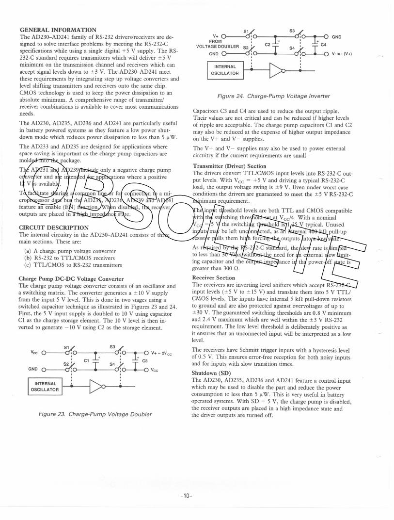
Charge Pump DC-DC Voltage ConverterThe charge pump voltage converter consists of an oscillator anda switching matrix. The converter generates a ::t10 V supplyfrom the input 5 V level. This is done in two stages using aswitched capacitor technique as illustrated in Figures 23 and 24.First, the 5 V input supply is doubled to 10 V using capacitorCl as the charge storage element. The 10 V level is then in-verted to generate -10 V using C2 as the storage element.
51/ ~ 3
vcc o cr;C '~ V+=2Vcc. + ' +'C1 ' C3
52 ~ - T 54';' T--GNDo cr:o 4 <::~ Vcc, ,, ,
~~
Figure 23. Charge-Pump Voltage Doubler
~--
51/ ~ 3V+ o <Ji(. .0-+-0 GND
FROM : + :.J.: ~.VOLTAGE DOUBLER S2./ C2 T S4';' T C4
GND 0--<:5:~:~ V-=-(V+). ,. ,~,~
INTERNAL
OSCILLATOR
Figure 24. Charge-Pump Voltage Inverter
Capacitors C3 and C4 are used to reduce the output ripple.Their values are not critical and can be reduced if higher levelsof ripple are acceptable. The charge pump capacitors Cl and C2may also be reduced at the expense of higher output impedanceon the V+ and V-supplies.
The V+ and V- supplies may also be used to power externalcircuitry if the current requirements are small.
Transmitter (Driver) SectionThe drivers convert TTL/CMOS input levels into RS-232-C out-put levels. With Vcc = +5 V and driving a typical RS-232-Cload, the output voltage swing is ::t9 V. Even under worst caseconditions the drivers are guaranteed to meet the ::t5 V RS-232-Cminimum requirement.
The input threshold levels are both TTL and CMOS compatiblewith the switching threshold set at Vcc/4. With a nominalVcc = 5 V the switching threshold is 1.25 V typical. Unusedinputs may be left unconnected, as an internal 400 kil pull-upresistor pulls them high forcing the outputs into a low state.
As required by the RS-232-C standard, the slew rate is limitedto less than 30 V/f.-lSwithout the need for an external slew limit-ing capacitor and the output impedance in the power-off state isgreater than 300 il.
Receiver Section
The receivers are inverting level shifters which accept RS-232-Cinput levels (::t5 V to ::tIS V) and translate them into 5 V TTL/CMOS levels. The inputs have internal 5 kil pull-down resistorsto ground and are also protected against overvoltages of up to::t30 V. The guaranteed switching thresholds are 0.8 V minimumand 2.4 V maximum which are well within the ::t3 V RS-232requirement. The low level threshold is deliberately positive asit ensures that an unconnected input will be interpreted as a lowlevel.
The receivers have Schmitt trigger inputs with a hysteresis levelof 0.5 V. This ensures error-free reception for both noisy inputsand for inputs with slow transition times.
Shutdown (SO)The AD230, AD235, AD236 and AD241 feature a control inputwhich may be used to disable the part and reduce the powerconsumption to less than 5 f.-lW. This is very useful in batteryoperated systems. With SD = 5 V, the charge pump is disabled,the receiver outputs are placed in a high impedance state andthe driver outputs are turned off.
-10-
---
OBSOLETE

, Enable InputThe AD235, AD236, AD239 and AD241 feature an enable in-put (EN). It is used to enable the receiver outputs. WithEN = 0 V the outputs are enabled. With EN = 5 V the outputsare placed in a high impedance state. This function allows theoutputs to be connected directly to a microprocessor data bus. Itcan also be used to allow receivers from different devices toshare a common data line. The timing diagram for the enablefunction is shown in Figure 25.
Figure 25. Enable Timing
) APPLICATION HINTS
Protection for Shorts to z15 V SuppliesThe driver outputs are internally protected against shorting toground, to other driver outputs, to V+ or to V-. In practice,these are the highest voltages likely to be encountered in an ap-plication. lithe possibility exists for shorting to :t 15 V, then itis recommended that external protection be provided. This maybe done by connecting a series 220 !1 resistor on each transmit-ter output.
)
AD230-AD241
Figure 26. Protection for Shorts to :!::15 V
)
Over.Voltag~ Protection for AD231, AD239The AD231 and AD239 require an external + 12 V supply asthey do not contain an internal V+ generator. It is importantthat this supply be switched on before the 5 V, Vcc supply.
If there is a possibility that the Vcc supply will be switched onfirst, or if the 12 V supply may be inadvertently shorted toground, then it is recommended that a diode (IN914 or equiva-lent) be connected in series with the 12 V input. This will notaffect normal operation but it ensures that under fault condi-tions, the device will be protected.
Figure 27. Diode Protection Scheme for AD231 and AD239
High Baud Rate OperationThe RS-232-C standard requires that "For Data and TiminginterchangeCircuits, the timefor the signal to pass through the tran-sition regionshall not exceed one millisecondorfour percent of thenominal duration of the signal elementon that interchangecircuit,whichever is the lesser." With the maximum transmission rate of19.2 kbaud, this translates into a minimum slew rate of 3 V/J.Ls.The typical slew rate of the AD230-AD241 is 3 V/J.Lsundermaximum loading conditions and therefore meets the standard.
The V.28 standard is more stringent and requires a transitiontime which will not exceed three percent of the nominal signalduration. This translates into a slew rate of 4 V/J.Lsat the maxi-mum 19.2 kbaud rate. In practice, less than ideal slew rates willhave negligible affect on the data transmission. The result is thatthe valid mark/space duration is slightly shorter than the opti-mum because the signal spends more time in the transition re-gion. The valid duration remains more than adequate for error-free reception even at maximum transmission rates and underworst case load conditions.
Driving Long CablesIn accordance with the RS-232-C standard, long cables are per-missible provided that the total load capacitance does not exceed2500 pF. For longer cables which do exceed this, then it is pos-sible to trade off baud rate vs. cable length. Large load capaci-tances cause a reduction in slew rate, and hence the maximumtransmission baud rate is decreased. The AD23D-AD241 aredesigned so that the slew rate reduction with increasing loadcapacitance is minimized.
For the receivers, it is important that a high level of noise im-munity be inbuilt so that slow rise and fall times do not causemultiple output transitions as the signal passes slowly throughthe transition region. The AD230-AD241 have 0.5 V of hystere-sis to guard against this. This ensures that, even in noisy envi-ronments, error-free reception can be achieved.
-11-~ --
3V
\EN
IovI I
I I
I I
TENI
T DlSII
.......- -... ..-)
I I
t3.SV
' VOH- O.1V
ROUT DATA VALID
O.8V +- VOL+O.1V
+SV +12V
Lf:.
Vcc V+
AD231 & AD239
{/OBSOLETE

ORDERINGINFORMATION
*= 0.6" DIP package (all other DIP packages = 0.3")
-12-
~--
Temperature Temperature TemperaturePart Range Package Part Range Package Part Range Package
AD230 AD23! AD232
AD230JN 0 to +70'C 20-Lead AD23IJN 0 to + 70'C 14-Lead AD232JN 0 to +70'C 16-LeadPlastic DIP Plastic DIP Plastic DIP
AD230JR 0 to + 70'C 20-Lead AD23IJR 0 to +70'C 16-Lead AD232JR 0 to +70'C 16-LeadSOIC SOIC SOIC
AD230AN -40'C to +85'C 20-Lead AD23IAN -40'C to +85'C 14-Lead AD232AN -40'C to +85'C 16-LeadPlastic DIP Plastic DIP Plastic DIP
AD230AR -40'C to +85'C 20-Lead AD23lAR -40'C to +85'C 16-Lead AD232AR -40'C to +85'C l6-LeadSOIC SOIC SOIC
AD230AQ -40'C to +85'C 20-Lead AD23lAQ -40'C to +85'C 14-Lead AD232AQ -40'C to +85'C 16-LeadCerdip Cerdip Cerdip
AD23ISQ -55'C to + l25'C 14-Lead AD232SQ -55'C to + l25'C l6-Lead
Cerdip Cerdip
AD233 AD234 AD235
AD233JN 0 to + 70'C 20-Lead AD234JN 0 to + 70'C l6-Lead AD235JN 0 to + 70'C 24-LeadPlastic DIP Plastic DIP Plastic DIP*
AD233AN -40'C to +85'C 20-Lead AD234JR 0 to + 70'C 16-Lead AD235AN -40°C to +85°C 24-LeadPlastic DIP SOIC Plastic DIP*
AD234AN -40°C to +85°C 16-Lead AD235AQ -40°C to +85°C 24-LeadPlastic DIP Ceramic*
AD234AR -40'C to +85°C 16-LeadSOIC
AD234AQ -40'C to +85°C 16-Lead
Cerdip
AD234SQ -55°C to + 125°C l6-Lead
Cerdip
AD236 AD237 AD238
AD236JN 0 to +70°C 24-Lead AD237JN 0 to + 70'C 24-Lead AD238JN 0 to + 70'C 24-LeadPlastic DIP Plastic DIP Plastic DIP
AD236JR 0 to + 70°C 24-Lead AD237JR 0 to + 70°C 24-Lead AD238JR 0 to + 70°C 24-LeadSOIC SOIC SOIC
AD236AN -40°C to +85°C 24-Lead AD237AN -40°C to +85°C 24-Lead AD238AN -40°C to +85°C 24-LeadPlastic DIP Plastic DIP Plastic DIP
AD236AR -40°C to +85'C 24-Lead AD237AR -40°C to +85°C 24-Lead AD238AR -40°C to +85°C 24-LeadSOIC SOIC SOIC
AD236AQ -40°C to +85°C 24-Lead AD237 AQ -40'C to +85°C 24-Lead AD238AQ -40°C to +85°C 24-LeadCerdip Cerdip Cerdip
AD236SQ -55°C to + 125°C 24-Lead AD238SQ -55°C to + 125'C 24-LeadCerdip Cerdip
AD239 AD24!
AD239JN 0 to +70°C 24-Lead AD24IJR 0 to +70°C 28-LeadPlastic DIP SOIC
AD239JR 0 to +70°C 24-Lead AD24lAR -40°C to +85'C 28-LeadSOIC SOIC
AD239AN -40'C to +85°C 24-LeadPlastic DIP
AD239AR -40°C to +85°C 24-LeadSOIC
AD239AQ -40°C to +85°C 24-Lead
Cerdip
AD239SQ - 55'C to + 125°C 24-Lead
Cerdip
OBSOLETE

)
)
)
)
)
14-Lead Plastic DIP (N-14)
04 8TPIN1 0.28017.111" 0.240 16.101
1 7 -1.. .
IV V 0.795 (20.19111 11 Ir-- 0.725118.421---1 0.06011.52)
.. ~ ,.," ,,~,
0.210
~15.33)SEATINGL-- - - - - - -
PLANE 0.20015.051
~ ~
to.150 (3.81)0.125 (3.181 l.
~~ -I i- 0.070(1.77)0.022 (0.5581 0.10012.54) 0.045 (1.1510.014 10.3561
16-Lead Plastic DIP (N-16)
""~~~:::::: ~I~:::::IV V V 0.840 (21.33) V V Ir--- 0.745118.931 10.060 11.521
-.-~.."'~'
0.210 ..(5.331 ----.
S~~~~O.~- - - - -
~
-
U
- t~~1~0.125(3.181 --L-,- ". . I I. 0.070 (1.771
-II'""" -I I'""" 0.045 (1.1510.02210.5581 0.10012.5410.01410.3561
16-Lead SOIC (R-16)
r-- 0.413(10.50)---1
I R R ,0.348(10.10)I R R-I~T0.29917.60)
0.291 (7.401
OUTLINE DIMENSIONS
0.325 (8.251
h10.30017.621.--Lr \ 0.19514.951
-~ ,T5 12.931
10.419 (10.65)
0.404 (10.26)
O.O50UUUUUUUU L11.27) -j I- -j I- 0.018 (0.46) t 0.364 (9.246)
jTYP 0.014 (0.361 0.344 18.738)+
6t::Jt::Jt::Jt::Jt::Jt::J~.i.~.id( ~ ~~====== t t T -+11-
0.010 (0.25) 0.015 (0.38) 0.045 11.15)0.004 (0.101 0.00716.18) 0.02010.501
14-Lead Cerdip (Q-14)
~: ~ ~ ~ ~ ~ I~I I:::I. 0.780 (19.81) -' . 0.300 17.6
~2)
r- ~ -1 r- REF
wmw '.'M"'"a0.133 (3.378)
~ 0.21+(5.33)
0.12~\~1711
L~3.81) 1f~
T--:[ +II.- -.J I- 0.012(0.305)0.0611.52) 0.0210.5) 0.1112.79) 0.008 (0.20310.05 (1.27) 0.016 (0.4061 0.09912.281
16-Lead Cerdip (Q-16)
[~~~ ~~~I~::=:II 0.300(7.62)
r-0.780(19.81)~~14.14) ir-REF=iJ
~"~"m' ~--.~ 0.21 (5.33) 150
0.12~\~17)1
L~.81) o~
~ II I I- 0.01210.3051-+j -I t+- -t 0 008 (0.20310061152) 0.0210.5) 0.11(2.791 .
0:0511:27) 0.016 (0.406) 0.09912.28)
lO-Lead Plastic DIP (N-lO)
- ,~ ~ : ~ ~ : : ~ ~ : ~ I ~:;:;:IV V V 'u1.060 (26.901 11 V 11 Ir 0.925 (23.50) I0.060 (1.52)
.~ '.m"'"
0.210 .15.331 --,
S~~~~O~I - - - - - - -
~
-
~- t r:ilil01
0.125(3.18) i..
~i- -j I-0.02210.5581 0.10012.541 0.07011.781O~01410.3561 0.045 (1.151
-13-
OBSOLETE

20-Lead Cerdip (Q-20)
f;:::,:I:,::::I~:~:::~i0.20 (5'0[J~ "kl(,10.14 13.56) 0.125 (3.18)
0.15 (3.81 - tJ 0.011 10.28)0.12513.18)
UII '
l
O'009(0.23)
,- ~ --H-- -J ~ "I0.02 10.5) 0.11 12.79) ~
0.016 10.411 0.09 (2.28) 00.07 (1.78)0.05 (1.27)
LEAD NO.1 IDENTIFIED BY DOT OR NOTCHLEADS ARE SOLDER OR TIN-PLATED KOVAR OR ALLOY 42
24-Lead Plastic DIP (N-24A)
10.55 (13.911
J3.411
I VVVVVVVVVVVV I
1.25 (31.15) 0.606 (15.41
L . 1.24131.5) . ~r--D~I I
u~ ...~,Ir ,I15.081 ~MAX =---*- ~~ 0115(4451 D.OI2(D.305)
J l ~.12(3.;") t 0.008(0.203) ~-01j.- ...j I- --r
0.065 (1.66) 0.02 (0.5081 0.105 (2.6110.45 (1.151 0.015 (0.38" D.'" (2.421
24-Lead Plastic DIP (N-24)
f0.260 ...00116.61 .0.031
---1.
I 1=131.19) I. 1.226(31.14) 1.
~.~~0.128(3.251
SEATI~- - - - - - - - - - -- - ---,
PLA -.j fo- -.j fo- j L --{.0.0210.51 0.1112.79' 0.07(1.78)
0.01610.41) ii]9jffij 0.0511.271
NOTES,. lEAD NO.1 IOEN""ED 8V OOT OR NOTCH.
2. PLASTIC LEADS WILL 8E EITHER SOLDER DIPPED OR TIN lEAD PLATEDIN ACCORDANCE WITH Mll.M.38510 REOUIREMENTS.
24-Lead Ceramic DIP (0-24)
..r::'~[~I~ : r~~
I I 10-- 0.610"5.491 I, 1.200(32.77) . 0.07511.911L_..~_I
.~--I~~ ~
SEA.zl~--'-- - - - -- - - - - - - -- 0.150 0.01510.38'0.200 15.G8I
J Lf 13.811 II 0.00810.20'
0.120 (3.051 ---1.. U~ II 0.
.02310.58' I I 0.07011.78' I 0.620 (15.751 I
""Ir+-001410.361 -t r+- 0.03010.76' "'--0.59011499'---"0.11012.791
0.090 12.291
24-Lead Cerdip (Q-24)
[::~~::::]JI I 0.3208128
~. 1.200(32.77IMAX. 1 0.200(7.3661
,J;;'~ <- =15.715) 14.572)MAX ~X
SEATlNG~ - - -- - - - - - - - - :::;:-t --PLANE 0.125 T 001210305113.1751
j L~ II
I0:00810:203,
MIN 0.02010.5081 U TV'
~~ -.j fo- --{~~~:i~;~~: ~~:g::: ~~~i:;;:: 1fTVP TVP
,. lEAD NO. llDENTlAED 8V OOT OR NOTCH.
2 CERDIP lEADS WILL 8E EITHER TIN PLATED OR SOLOER OIPPEDIN ACCORDANCE WITH Mll.M.3"'0 REQUIREMENTS.
-14-
OBSOLETE

)
)
)
)
:~:Jr~~ ~ ~ ~ ~;:'::o:c;;~~, :+j~ ~ ~ ~ ~ ~ ~ ~ ~~ ~ ~ ~ ~I~.~::
.,:: '.'"
I I. ~ .- ,,-, .1..""" .. .".
I
~ "696(17671 --L -+jt+- 0.01310.321-'u r--, ,..,_.
0608(15.451 0.0'612.441 00210.511 ~-iI.~ ~ ~ ~ ~... "." .~. ~, ., ,.. ".., l1J-1J-1J-1J-1J-1J-1J-1J-1}-1}-1J-1HI-1JL*,T,~ I"r--- , , I~ ~, " -II- """", 0 -- 10-~~ L~,J. ~ I- 0
.01910
.491 0.00610151 0..0421'
.
0671
-'fT -F-.c j I! 00511271 00141035) 0018104571
I I -II- 0.01 10.2541
-+f t- ~ 000610151 0.04211.05710.05 (1.271 0.'014 (0.351 " 0.018 (0.4571
28-Lead SOIC (R-28)
,. LEAD NO.1 IDENTIFIED BY A DOT.
2. SOIC LEADS WILL BE EITHER TIN PLATED OR SOLDER DIPPEDIN ACCORDANCE WITH MIL.M.'851O REQUIREMENTS.
,. LEAD NO. "DENTIF'ED BY A DOT
2. SOIC LEADS WILL BE EITHER TIN PLATED OR SDLDER DIPPEDIN ACCORDANCE WITH MIL.M.'851O REQUIREMENTS
-15-
-~ -
OBSOLETE