Embed Size (px)
Citation preview

PRECISION CMOS RECEIVERS FOR VLSI TESTING
APPLICATIONS
A DISSERTATION
SUBMITTED TO THE DEPARTMENT OF
ELECTRICAL ENGINEERING
AND THE COMMITTEE ON GRADUATE STUDIES
OF STANFORD UNIVERSITY
IN PARTIAL FULFILLMENT OF THE REQUIREMENTS
FOR THE DEGREE OF
DOCTOR OF PHILOSOPHY
Daniel K. Weinlader
November 2001

ii
© Copyright by Daniel K. Weinlader 2001
All Rights Reserved

iii
I certify that I have read this dissertation and that, in my opinion, it is fully adequatein scope and quality as a dissertation for the degree of Doctor of Philosophy.
Mark A. Horowitz Principal Adviser
I certify that I have read this dissertation and that, in my opinion, it is fully adequatein scope and quality as a dissertation for the degree of Doctor of Philosophy.
Thomas H. Lee
I certify that I have read this dissertation and that, in my opinion, it is fully adequatein scope and quality as a dissertation for the degree of Doctor of Philosophy.
James A. Gasbarro
Approved for the University Committee on Graduate Studies:

iv
v
Abstract
Testing CMOS parts is becoming more difficult due to the proliferation of high-speed I/O
circuits that operate at frequencies exceeding the performance capabilities of modern
testers. The performance gap between high-speed chip I/O frequencies and tester
frequencies is further extended by the rapid performance scaling of CMOS, compared to
bipolar and GaAs technologies which are commonly used in tester electronics.
Furthermore, as VLSI parts integrate increased amounts of functionality and become more
complex, testing of the parts becomes more difficult due to insufficient observability of
the high-speed interactions between circuits within the chip. Integrating high-speed test
capabilities onto production die would permit testing of parts incorporating high-
frequency I/O in addition to increasing the observability of internal signals on the die.
The key challenge is to achieve high-precision timing measurements using a process
technology that may be no better than the one used to build the part being tested. To
overcome the frequency limitations of the process technology, an oversampled receiver
with time-interleaved samplers clocked by a multi-phase clock generator is utilized. While
this enables a high receiver sample rate, sampler input offsets and static phase spacing
errors in the clocks limit timing accuracy. This dissertation presents techniques to measure
and compensate for static errors in both the clock generator and input samplers. In
addition to static errors, jitter in the clock generator can significantly degrade timing
accuracy. Therefore, a technique that measures and subtracts jitter from the timing
measurements is proposed.
The aforementioned techniques enable the construction of an input receiver with
timing accuracy suitable for testing applications and are demonstrated with a 0.25µm
CMOS test chip. Techniques are also presented to integrate a small oversampling receiver
onto VLSI parts to increase observability and enable timing measurements of internal
signals.

vi

vii
Acknowledgments
“Art is I; science is we.” - Claude Bernard
While this work solely bears my name as the author, it is actually the result of efforts on
the part of many people.
This work would not have been possible without the guidance and wisdom of my
advisor, Mark Horowitz. He has been both generous with his time and patient and as a
result, I have benefitted greatly from my interactions with him. A large part of this thesis
is based on work by students who preceded me, Stefanous Sidiropolous, Chih-Kong Ken
Yang, John Maneatis and Jim Gasbarro. I can only hope future students will find this work
as beneficial. I have been fortunate to work with many wonderful people including, Ken
Mai, Bharadwaj Amrutur, James Smith and Gu-Yeon Wei. They have made my research
more productive and my time spend at Stanford enjoyable. Ron Ho deserves special
mention, not only as a good friend, but for all his help in construction of the test chip. He
spent countless hours with unselfish dedication, certainly more than anyone could or
should ask of a friend.
While the research and researchers are the primary focus of attention at Stanford, there
are a great number of support people who make the work possible. Those who I have had
the privilege of working with include Darlene Hadding, Deborah Harber, Charlie Orgish
and Joe Little.
My parents taught me the importance of dedication, perseverance, and work ethic, and
as a result, my dissertation is a product of their efforts as much as it is of mine. My
brother, John, and sister, Karen, have provided me with much support and encouragement.
This work has required a great deal of patience, support and love from my wife,
Terese, for which I am eternally grateful. My son Nolan and daughter Audrey have, truth
be told, hindered more than helped the completion of this work, but they give new purpose
to everything I do and therefore I would be remiss not to mention them.

viii

ix
Contents
Abstract ............................................................................................................................................vAcknowledgements....................................................................................................................... viiList of Figures ................................................................................................................................ xi
Chapter 1: Introduction ................................................................................................................11.1 Test Overview......................................................................................................................11.2 Goals ....................................................................................................................................4
1.2.1 Organization................................................................................................................4
Chapter 2: Background................................................................................................................ 52.1 The Allure of CMOS ...........................................................................................................52.2 I/O Channel Requirements...................................................................................................82.3 Timing Performance ..........................................................................................................10
2.3.1 Detailed Timing Information ....................................................................................112.3.2 Over-Sampling Receiver...........................................................................................12
Chapter 3: Timing Accuracy ......................................................................................................153.1 Multi-Phase Clock Generation...........................................................................................153.2 Timing Accuracy ...............................................................................................................183.3 Static Phase Offsets ...........................................................................................................19
3.3.1 Sources of Static Phase Offset ..................................................................................203.3.2 Measurement and Calibration ...................................................................................22
3.4 Deterministic Jitter.............................................................................................................243.4.1 Measurement and Compensation..............................................................................26
3.5 Input Samplers ...................................................................................................................273.6 Summary ............................................................................................................................30
Chapter 4: Implementation and Timing Performance ............................................................334.1 Test Chip............................................................................................................................334.2 Clock Generation ...............................................................................................................34
4.2.1 Basic Elements..........................................................................................................344.2.2 Delay-Line Based Clock Generator ..........................................................................384.2.3 Ring Oscillator Based Clock Generator....................................................................41
Adjustable Interpolation ..............................................................................................44Array Layout ................................................................................................................46
4.2.4 Control Loop Design ................................................................................................474.2.5 Clock Drivers ............................................................................................................504.2.6 Measured Phase Results............................................................................................514.2.7 Phase Alignment Considerations ..............................................................................54
Duty Cycle ...................................................................................................................564.2.8 Phase Adjustment Summary .....................................................................................574.2.9 Timing Jitter..............................................................................................................57

x
4.3 Samplers.............................................................................................................................634.3.1 Offset Compensation ................................................................................................664.3.2 Aperture ....................................................................................................................69
4.4 Floorplan ............................................................................................................................694.5 Summary ............................................................................................................................71
Chapter 5: Integrated Testing ....................................................................................................735.1 A Minimal Sampling System.............................................................................................735.2 Output Data........................................................................................................................79
5.2.1 Compression and Decimation ...................................................................................795.2.2 Jitter Compensation ..................................................................................................825.2.3 Edge Filtering ...........................................................................................................83
5.3 Testing the Tester...............................................................................................................835.4 Conclusion .........................................................................................................................84
Chapter 6: Conclusion.................................................................................................................85
Appendix A...................................................................................................................................89
References.....................................................................................................................................95

xi
List of FiguresFigure 1.1: Basic tester architecture ....................................................................................2
Figure 2.1: Comparison of fT for GaAs, Bipolar and CMOS devices .................................6
Figure 2.2: A modern VLSI tester (Teradyne J973) ............................................................7
Figure 2.3: Pin count trends .................................................................................................8
Figure 2.4: A time digitizer................................................................................................11
Figure 2.5: An oversampled receiver.................................................................................12
Figure 2.6: Fanout-of-4 inverter delay...............................................................................13
Figure 2.7: A CMOS implementation of an over-sampling receiver ................................13
Figure 3.1: Multi-phase clock generators ..........................................................................16
Figure 3.2: Interpolator operation......................................................................................18
Figure 3.3: Sample DNL and INL for a six-phase clock generator ...................................19
Figure 3.4: Multiple clock phases and their noise sensitivity functions ............................21
Figure 3.5: Histogram measurement of static clock phase alignment ...............................23
Figure 3.6: DLL and PLL jitter accumulation ...................................................................25
Figure 3.7: Ideal input sampler ..........................................................................................27
Figure 3.8: Differential input receiver with non-idealities ................................................28
Figure 3.9: Effect of input offset voltage on timing accuracy ...........................................30
Figure 4.1: Test chip block diagram ..................................................................................34
Figure 4.2: Differential delay element ...............................................................................35
Figure 4.3: Replica bias generator for delay elements.......................................................35
Figure 4.4: Differential interpolator...................................................................................36
Figure 4.5: An adjustable interpolator with a 3-bit adjustment range ...............................37
Figure 4.6: Initial interpolation strategy for DLL..............................................................38
Figure 4.7: Interconnect techniques for phase interpolation..............................................39
Figure 4.8: Final DLL interpolation topology ...................................................................40
Figure 4.9: DLL interconnect wrap around .......................................................................41
Figure 4.10: Multiple, uncoupled ring oscillators..............................................................42
Figure 4.11: Coupled rings with top and bottom rings uncoupled ....................................43
Figure 4.12: Fully interconnected ring oscillators .............................................................43
xii
Figure 4.13: Four by five array oscillator ..........................................................................44
Figure 4.14: Array oscillator layout...................................................................................46
Figure 4.15: PLL control loop ...........................................................................................47
Figure 4.16: DLL control loop...........................................................................................48
Figure 4.17: Control loop charge pump.............................................................................49
Figure 4.18: Reduced ripple charge pump.........................................................................50
Figure 4.19: Low-to-high swing converter and clock buffers ...........................................51
Figure 4.20: Architecture for histogram measurements of phase offsets ..........................52
Figure 4.21: Histogram plot of interpolator output............................................................53
Figure 4.22: Correlation of histogram measurements to phase spacing ............................54
Figure 4.23: Compensated DLL phase spacing .................................................................55
Figure 4.24: Adjustable timing vernier with buffer delay range .......................................56
Figure 4.25: Low-swing constant current output driver ....................................................58
Figure 4.26: Timing jitter with no induced noise ..............................................................59
Figure 4.27: Timing jitter with induced noise ...................................................................60
Figure 4.28: Sampler configuration for sampling high-frequency jitter............................62
Figure 4.29: Correlation of high-frequency DLL jitter......................................................63
Figure 4.30: Input sampler.................................................................................................64
Figure 4.31: Monte-Carlo analysis of sampler offset voltage ...........................................65
Figure 4.32: Input sampler with offset compensation .......................................................65
Figure 4.33: Histogram plot of sampler input referred offset voltage ...............................66
Figure 4.34: Measured sampler offset adjustment range ...................................................66
Figure 4.35: Sampler offset compensation stability versus temperature ...........................67
Figure 4.36: Sampler offset compensation stability versus input common-mode.............67
Figure 4.37: Sampler beta compensation stability versus common-mode ........................68
Figure 4.38: Sampler step and impulse responses .............................................................68
Figure 4.39: Frequency spectrum of sampling impulse.....................................................69
Figure 4.40: Experimental test chip micrograph ...............................................................70
Figure 5.1: Interconnect between instrumented logic and sampling system .....................75
Figure 5.2: Topology for measuring interconnect delay....................................................76
Figure 5.3: Increasing static delay measurement with induced jitter.................................77

xiii
Figure 5.4: Matching for 800µm of interconnect ..............................................................78
Figure 5.5: Logarithmically encoded edge information ....................................................80
Figure 5.6: Window based decimation of sampler data.....................................................81
Figure 5.7: Edge detection and compression .....................................................................81
Figure 5.8: Real-time jitter compensation .........................................................................82
Figure A.1: Interpolator operation .................................................................................... 89
Figure A.2: Interpolator model ..........................................................................................90
Figure A.3: Linearity of interpolator model with unit step inputs.....................................90
Figure A.4: Interpolator current versus input rise time .....................................................91
Figure A.5: Linearity of interpolator model with finite-risetime inputs............................93
Figure A.6: Linearity of interpolator SPICE model ..........................................................93

xiv
1.1 Test Overview
1
Chapter 1
Introduction
“If I had more time, I would write a shorter story.”
- Mark Twain
Every CMOS VLSI chip that is produced needs to be tested to ensure it was manufactured
correctly. Test and possible debug has always been a challenging task that requires
specialized hardware “testers.” Furthermore, the rapid scaling of chip performance is
making test increasingly difficult. Until recently, testers were able to leverage process
technologies with intrinsic performance greater than CMOS to obtain sufficient timing
capabilities to accurately test CMOS parts. However, because the performance of CMOS
technology has scaled faster than the performance of other process technologies, using
non-CMOS process technologies to build testers suitable for testing modern VLSI parts is
becoming more difficult.
CMOS process scaling has not only enabled faster clock rates, but also increased chip
functionality. As technology scales, more complex designs can be integrated on a chip to
improve performance, because on-chip communication is vastly faster than external
interconnects. However, an undesirable effect of integration is a reduction in the
observability of the system, and, as a result it is more difficult and costly to test and debug
a part. Building the tester pin electronics in CMOS and in some cases, even integrating the
pin electronics into production parts can address both performance and observability and
lead to easier test and debug. This thesis addresses key issues in building high-speed
testers in CMOS.
1.1 Test OverviewThe purpose of a VLSI tester is to drive a part with known values and to verify that the
outputs of the part are correct. In addition to pass/fail production test, testers are also used
for debugging and performance characterization. A block diagram of a tester’s basic

1.1 Test Overview
2
function blocks is shown in Figure 1.1. While this figure only shows a single transmitter
and receiver channel, modern testers are typically composed of hundreds, or thousands, of
such channels. The device under test (DUT) is socketed on a custom printed circuit board
(PCB), known as a load board, that interfaces the part to the tester. The tester drives the
DUT with data vectors that are either algorithmically generated at run time or pre-
generated and stored in a memory. The tester samples the DUT outputs and compares
them to expected values which are also read from memory or generated on-the-fly. The
pin electronics drives input data and samples the DUT with specified timing. Building
high-speed pin electronics with precise timing that can scale with the performance of
CMOS parts is a significant challenge.
The I/O frequencies of CMOS parts have historically scaled in a very limited manner
primarily due to signal integrity issues at the system level [15].1 This has been beneficial
for test because the same tester could be used to test multiple generations of CMOS parts.
But eventually higher speed I/O is required because insufficient chip I/O bandwidth limits
the part functionality. This problem has been partly addressed by increasing the number of
1. As an example, the I/O bus on Intel IA32 processors has increased in frequency by a factor offour (33MHZ to 133Mhz) over a period of roughly a decade (from 1990 to 2000). However, pro-cessor performance has increased by roughly a factor of thirty over the same period.
Timing Generator
Timing Generator
DUTData
Generator
DataAcquisition Rx
Tx
Pin Electronics
Input to DUT
Outputof DUT
Figure 1.1: Basic tester architecture
1.1 Test Overview
3
I/O pins with advanced packaging techniques, such as flip-chip bonding, but these
solutions are limited by routing considerations in both the chip substrate and the printed
circuit board. Further efforts have focused on high-speed I/O techniques, which are
becoming an increasingly common method for improving system bandwidth. This is
evident in high-end networking chips, which can have I/O frequencies in excess of 3GHz
[45], and in more mainstream systems, such as personal computers, that contain a number
of parts with high-speed interfaces such as RDRAM [44], DDR-SDRAM [43], and AGP
[42] graphics chips.
Testing parts with high-speed I/O is difficult because data must be driven and sampled
by the tester at high frequencies and with precise timing. In the past, manufactures of test
equipment have been able to leverage the intrinsic performance of expensive process
technologies, such as Gallium Arsenide (GaAs) and Silicon bipolar. These technologies,
while not supporting the integration densities of CMOS, have had faster devices and thus
could be used to build a tester with sufficient performance to test CMOS parts. However,
the performance of CMOS technology now matches or exceeds the performance of many
GaAs and bipolar technologies, primarily due to the larger research and development
efforts directed towards it. The result is that performance of technologies that have
historically been faster than CMOS, such as GaAs, can no longer be leveraged to build
testers capable of testing the fastest CMOS parts.
The increase in chip and I/O frequencies has not only made traditional testing more
difficult but has also created a demand for more advanced test and measurement
capabilities. Modern testers obtain minimal timing information because they only test the
output of a part at specified times for the correct value. However, knowing when edges
transition is more useful when dealing with timing issues. For debugging, edge transition
information allows a better understanding of the characteristics and effects of jitter. For
production, this information can potentially enable faster characterization of part
performance and margins.
An alternative to building parts with high-speed I/O is integrating the parts that must
communicate at high speeds onto a single chip (termed a system-on-a-chip or SOC for
short). While this avoids the problems of testing parts with high-speed interfaces, the

1.2 Goals
4
communication between components integrated on the SOC can no longer be easily
observed because probing on-chip signals is much more difficult than probing printed
circuit board traces. This makes test and debug more difficult and expensive. A solution to
this problem is to embed part of the tester onto the die so that it can capture the state of the
internal signals and restore observability.
1.2 GoalsThe goal of this thesis is to build a CMOS input receiver with high timing accuracy
and edge-detection capabilities that is suitable for both stand-alone and embedded testing
applications. This work is focused on receivers rather than transmitters because edge
detection requires more sophisticated receivers, but not transmitters, and for embedded
applications, a receiver is more useful because it increases circuit observability.
1.2.1 Organization
To better understand tester constraints and technology options, Chapter 2 surveys the
evolution of tester technology and existing research work. This includes state-of-the-art
testers, experimental CMOS tester architectures and future trends. Challenges and
requirements of next-generation testers are described which leads to a promising
approach, CMOS oversampled receivers. Oversampled receivers can record detailed
timing information and are well suited for implementation in CMOS. CMOS however, has
not been historically competitive with GaAs and bipolar for building circuits with precise
timing. Therefore, Chapter 3 investigates the timing limitations of a CMOS oversampled
receiver. It includes the sources and characteristics of timing errors and compensation
techniques which make CMOS timing accuracy competitive with other process
technologies. Chapter 4 explores the implementation issues of a CMOS, multi-channel,
oversampled receiver and presents experimental results for the compensation techniques
presented in Chapter 3. As parts gets larger and more complex, integrating tester receivers
onto production part becomes more attractive. Chapter 5 considers the issues involved
including required hardware, inter-connect issues, and data processing. Chapter 6
concludes this work.

2.1 The Allure of CMOS
5
Chapter 2
Background
“A man with a watch knows what time it is. A man with two watches is never sure.”
- Segal's Law
The evolution of VLSI parts has required changes in tester design. In the past, the changes
have been primarily focused on I/O pin density rather than operating frequency or timing
accuracy because the technologies used to build pin electronics, bipolar and GaAs, were
well suited for high performance applications, but less capable of supporting high levels of
integration. Prior research has explored CMOS alternatives to address the integration
issues, but because of the performance gap between CMOS and bipolar or GaAs, pin
electronics continue to be built with GaAs or bipolar.
CMOS is a very attractive technology because the performance and integration is
scaling at a sustained rate that is faster than any other process technology. The next section
examines how the advantages of CMOS relate to testing and the potential benefits of a
CMOS tester. This is followed with two sections, 2.2 and 2.3, that expand on integration
and performance issues, which are the two primary issues confronting the design of
testers. All described in Section 2.3 are some promising circuits that provide sufficient
performance for high speed test and prepares the reader for a more detailed examination of
the timing issues presented in Chapter 3.
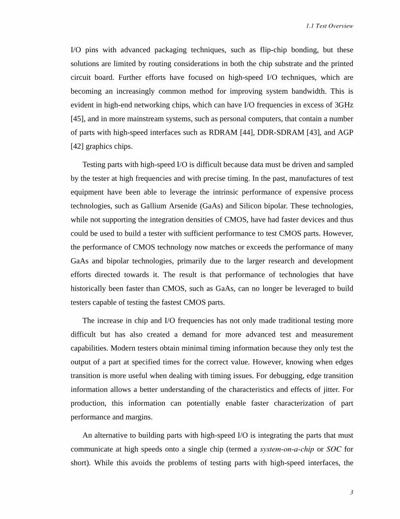
2.1 The Allure of CMOSTester pin electronics are commonly built in GaAs and bipolar technologies because
they have historically had a performance advantage over CMOS, but the rapid scaling of
CMOS technology makes it an attractive alternative, as evident in Figure 2.1. Because of
2.1 The Allure of CMOS
6
the rapid scaling of CMOS, extrapolating the data in Figure 2.1 indicates that in the near
future, the performance of CMOS devices will exceed that of GaAs and bipolar devices.
While the performance of CMOS devices is just becoming comparable with GaAs and
bipolar devices, CMOS does have the distinct advantage of superior process integration.
This enables the construction of highly integrated testers that can support the large
numbers of pins required by modern parts. Using technologies with less integration
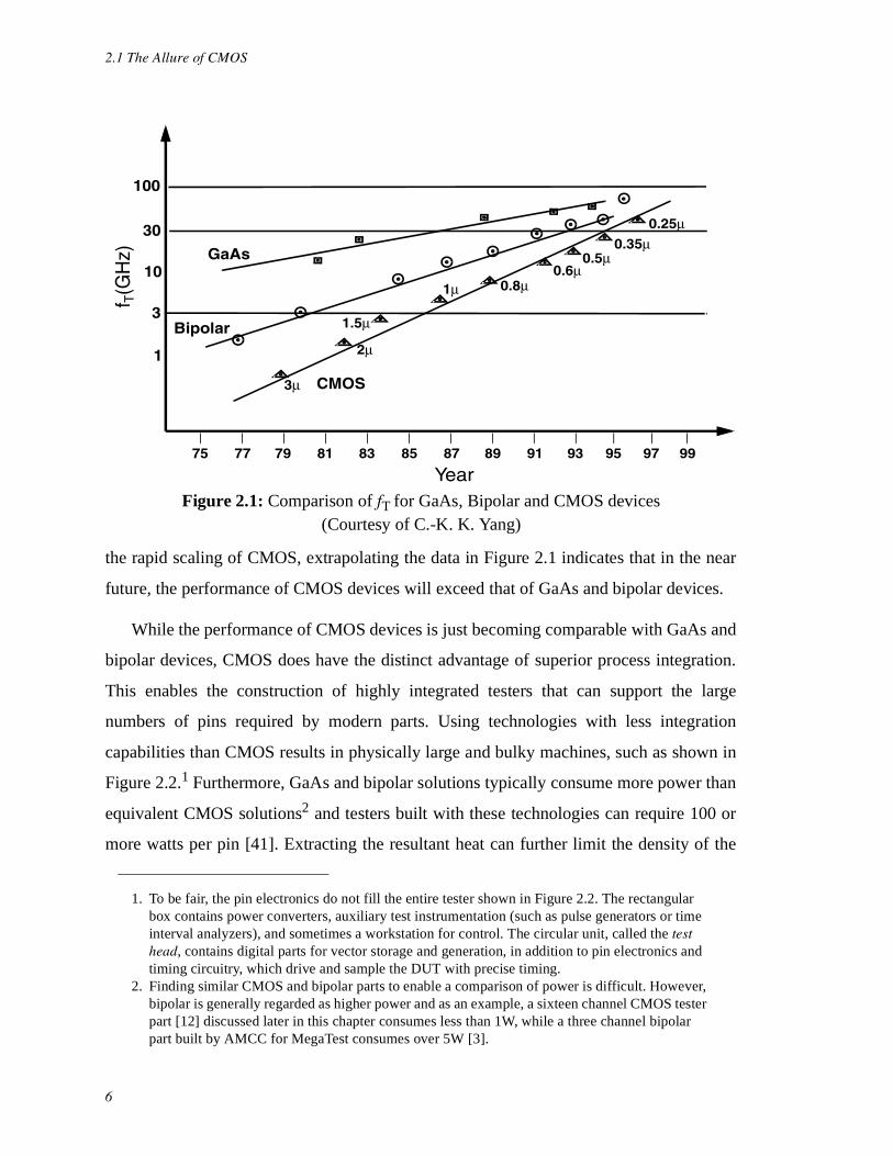
capabilities than CMOS results in physically large and bulky machines, such as shown in
Figure 2.2.1 Furthermore, GaAs and bipolar solutions typically consume more power than
equivalent CMOS solutions2 and testers built with these technologies can require 100 or
more watts per pin [41]. Extracting the resultant heat can further limit the density of the
1. To be fair, the pin electronics do not fill the entire tester shown in Figure 2.2. The rectangularbox contains power converters, auxiliary test instrumentation (such as pulse generators or timeinterval analyzers), and sometimes a workstation for control. The circular unit, called the testhead, contains digital parts for vector storage and generation, in addition to pin electronics andtiming circuitry, which drive and sample the DUT with precise timing.
2. Finding similar CMOS and bipolar parts to enable a comparison of power is difficult. However,bipolar is generally regarded as higher power and as an example, a sixteen channel CMOS testerpart [12] discussed later in this chapter consumes less than 1W, while a three channel bipolarpart built by AMCC for MegaTest consumes over 5W [3].
10
1
75 77 79 81 83 85 87 89 91 93
3µ
2µ
1.5µ
1µ 0.8µ0.6µ
GaAs
CMOS
f T(G
Hz)
Year95 97 99
0.5µ0.35µ
0.25µ30
100
3Bipolar
Figure 2.1: Comparison of fT for GaAs, Bipolar and CMOS devices(Courtesy of C.-K. K. Yang)
2.1 The Allure of CMOS
7
electronics. Because of these integration constraints, bipolar and GaAs pin electronics are
usually not highly integrated and one or more parts are required per pin. However, given
the integration potential of CMOS, significantly more integrated testers are feasible. A
decade old CMOS part presented in the next section integrates sixteen I/O channels and it
is reasonable to envision even higher integration using more modern CMOS processes.
In a sense, modern chip testers are analogous to mainframe computers. They are both
hand assembled to custom specifications provided by the customer, they eschew high-
integration for the sake of performance and the result is similar: large, expensive machines
that cost millions of dollars. In years past, the cost of a mainframe was justified by using it
to serve many users via remote terminals. Modern testers are similar: to lower the
amortized cost of testing, many parts are tested in parallel on a single tester.
The problem with the mainframe model is that despite being amortized across many
desktops, they are still expensive. Furthermore, the complexity of the machines makes the
design cycles long. For processors, new and simpler solutions that better leverage the
advantages of CMOS have significantly closed the performance gap. The result is that
mainframes are now confined to a niche market, while personal computers proliferate. If
testers were to follow a similar path, the result would be smaller, less expensive and
higher-performance machines.
Figure 2.2: A modern VLSI tester (Teradyne J973)

2.2 I/O Channel Requirements
8
2.2 I/O Channel RequirementsThe cost and size of a tester is greatly influenced by the number of I/O channels it
contains. Unfortunately, as CMOS VLSI parts increase in performance and functionality
so do the I/O requirements. This is quantified by the empirical formula known as Rent’s
rule:
where Np is the number of external connections, Ng is the number of gates on the chip,
and Kp and β are empirically determined constants. When originally formulated, this
equation assumed that the I/O speed was the same as that of the internal clock, however, in
modern parts this is not the case. Nevertheless, the observation that an increase in I/O is
required as parts become larger and more complex, is still valid and historical data
indicates that the number of I/O pins on a chip has scaled by about 12% per year as shown
in Figure 2.3 [8]. Contemporary testers can have thousands of pins and must continue to
scale with the pin counts of VLSI parts.
1980 1985 1990 1995 2000 2005 201010
1
102
103
104
Figure 2.3: Pin count trends
Year
Pin
Co
un
t
Np Kp Ngβ,⋅=

2.2 I/O Channel Requirements
9
Physically large pin electronics are required to support large numbers of I/O channels
because of limited integration. Connecting the pin electronics to the DUT then requires
long cables or PCB traces. If the wavelength of the highest frequency of interest is
comparable to the length of the signal path, then the connection cannot be viewed as a
lumped model and the transmission line characteristics, such as reflections, must be taken
into account. Reflections will distort the waveform unless the line is properly terminated,
but this is only possible if the driver is capable of driving the termination impedance.
While most tester pin electronics and high-speed I/O drivers are capable of driving
terminated transmission lines, this is not a general characteristic of all CMOS parts.
Furthermore, frequency dependant attenuation in the transmission line can still reduce
timing accuracy even in a properly terminated transmission line1. The result is that small,
integrated pin electronics are desirable to maintain short signal paths between the tester
and DUT.
To achieve better integration and lower costs, two CMOS architectures, the Data
Generator Receiver (DGR) and Testarossa, were developed at Stanford University in the
late 1980’s. Increased integration permits the placement of multiple I/O channels and
additional tester circuitry onto a single die. This enables the construction of testers with
large numbers of I/O channels while at the same time, maintaining short signal paths
between the tester and DUT.
The DGR integrated sixteen I/O channels and a 256 cycle vector memory onto a single
chip [23]. It was intended only for functional test and therefore could only to drive and
sample the DUT on clock cycle boundaries. Nevertheless, this part demonstrated the
feasibility of building a complete single-chip, CMOS functional tester.
The Testarossa improved on the DGR by adding pin electronics and timing
capabilities [12]. Pin electronics enable the tester to drive more complex waveforms than
the DGR for richer test capabilities. The timing features allow the tester to generate output
and sampling signals that transition at arbitrary locations within the clock cycle. Tunable
1. Dielectric loss and skin effect are the dominant loss mechanisms in printed circuit boards andcables, respectively. Attenuation of the high-frequency components can cause intersymbol inter-ference which is a form of a data dependant timing error.

2.3 Timing Performance
10
timing verniers constructed from static CMOS gates permitted fine edge placement.
Precise timing accuracy was achieved by using a high-precision external delay generator.
Because timing issues such as skew and jitter were not significant issues at the time
the Testarossa was built (1989), little attention was focused on these issues when
designing the circuits. So while the Testerossa demonstrated the potential of CMOS
testers, it lacked sufficient timing performance to test modern parts and unfortunately,
these timing issues are only becoming worse.
2.3 Timing PerformanceIdeally, a tester drives data to the DUT and samples the outputs at exact moments in
time as specified by the test program. However, timing uncertainty limits the accuracy of
when an edge is driven or when an output is sampled. This timing uncertainty is due to
both the tester pin electronics and the connection between the tester and DUT.
To compensate for this uncertainty, testers are run conservatively with a timing margin
that is sufficiently large to ensure a part that cannot meet timing requirements will not be
incorrectly marked as functional. This timing margin is termed the guard band and is
equal in magnitude to the timing error of the tester. The larger the tester guard band, the
more conservative the test margin. Conservative testing implies that marginal parts are
discarded despite meeting specified timing requirements. As I/O rates increase, the size of
the required guard band is an important parameter and timing uncertainty becomes a
critical performance metric for VLSI testers.
Unfortunately, the timing accuracy of testers is not scaling with the cycle time which
is a problem because they are consuming an increasing large percentage of the cycle. A
tester for 100MHz SDRAM has a cycle time of 10ns and a timing uncertainty +/-125ps
[46]which is 2.5% of the cycle, but a modern RDRAM tester has +/- 50ps uncertainty,
which is 8% of a 800MHz cycle [41]. The implies that parts with high-speed I/O either
have a lower yield or are binned into slower frequency ranges because of tester
limitations.
Testing methodologies can increase the impact of guard bands because it is not
uncommon for parts to be tested by multiple parties while transitioning from

2.3 Timing Performance
11
manufacturing to final product integration. If each party tests the parts with the same
guard band, then it is possible for the part to pass an initial test but fail a subsequent test. It
is important that the supplier provides the integrators with parts that meet or exceed the
published timing specification. Testing a part with a double guard band ensures that it will
always pass tests that use a single guard band. However, a double guard band provides no
margin for error and so at times, manufactures test with an even more conservative triple
guard band.
2.3.1 Detailed Timing Information
One way to reduce some of the overhead due to guard bands is to capture edge timing
information. Traditional testers verify DUT outputs by sampling at preset positions within
the cycle to determine if the outputs are correct. But knowing when edges transition
enables a test program to interpret the magnitude of a timing failure rather than treating all
errors as identical.
Edge timing information also provides cycle to cycle jitter and timing margin
measurements which are very useful when characterizing high-speed designs. Zargari
recognized the need for increased timing information during testing and the result was a
BiCMOS time digitizer that incorporates edge detection capabilities for 2 input channels
[37]. A simplified block diagram for the time digitizer architecture is shown in Figure 2.4.
The input signal clocks a register that captures the state of a high-speed counter to record
the time of the input transition. The resolution of the part is 90ps with an accuracy of 38ps
Multi-Phase ClockGenerator
RegisterClockDriver
InputRef.
Register ClockDriver
InputRef.
Figure 2.4: A time digitizer

2.3 Timing Performance
12
in a 0.6um BiCMOS process. High levels of integration are possible by sharing the multi-
phase clock generator among multiple input channels.
An interesting characteristic of the time digitizer is that it only outputs a digital value
when the input edge transitions. Thus, the output data rate is set by the number of
transitions of the input. For some applications where timing information is desired for
relatively infrequent events, such as physics experiments, this results in a form of output
data compression. However, in a tester application, sampling on transitions is less of an
advantage because the inputs can transition at higher rates which result in a large output
data bandwidth. Furthermore, the output data rate is dependent on the input transition rate.
A series of closely spaced input edges can cause the output data from one edge to
overwrite the data from a previous edge.
The main limitations of this approach are due to the data signal being used as a clock.
The input samplers require a clock of finite width, so narrow data glitches cannot be
captured. Low-swing input signals are also a problem because they are less effective as
clocks compared to full-swing signals. This is a significant problem because low-swing
signals are common in high-speed I/O. The clock can be amplified to full-swing, but the
amplifier will add timing uncertainty to the system.
2.3.2 Oversampling Receiver
Switching the role of the clock and data results in an oversampled receiver that
eliminates the drawbacks associated with the time digitizer. A block diagram of an
oversampled receiver is shown in Figure 2.5. By sampling the data signal at a very high
Clock Generator
D QInput @ freq = f
Freq = nf
n = oversampling rate
output bit-rate = nf bits/sec
0 0 1 1 0 0 0 1 1 1 1 1
2x oversamping
bit-time boundries
input
output data
Figure 2.5: An oversampled receiver
2.3 Timing Performance
13
rate, as compared to the input frequency, input transitions are captured with precise
timing. If a cycle is defined as 1/f where f is the maximum input frequency, then the
number of samples in a cycle is termed the oversampling rate (or for brevity, just the
sampling rate).
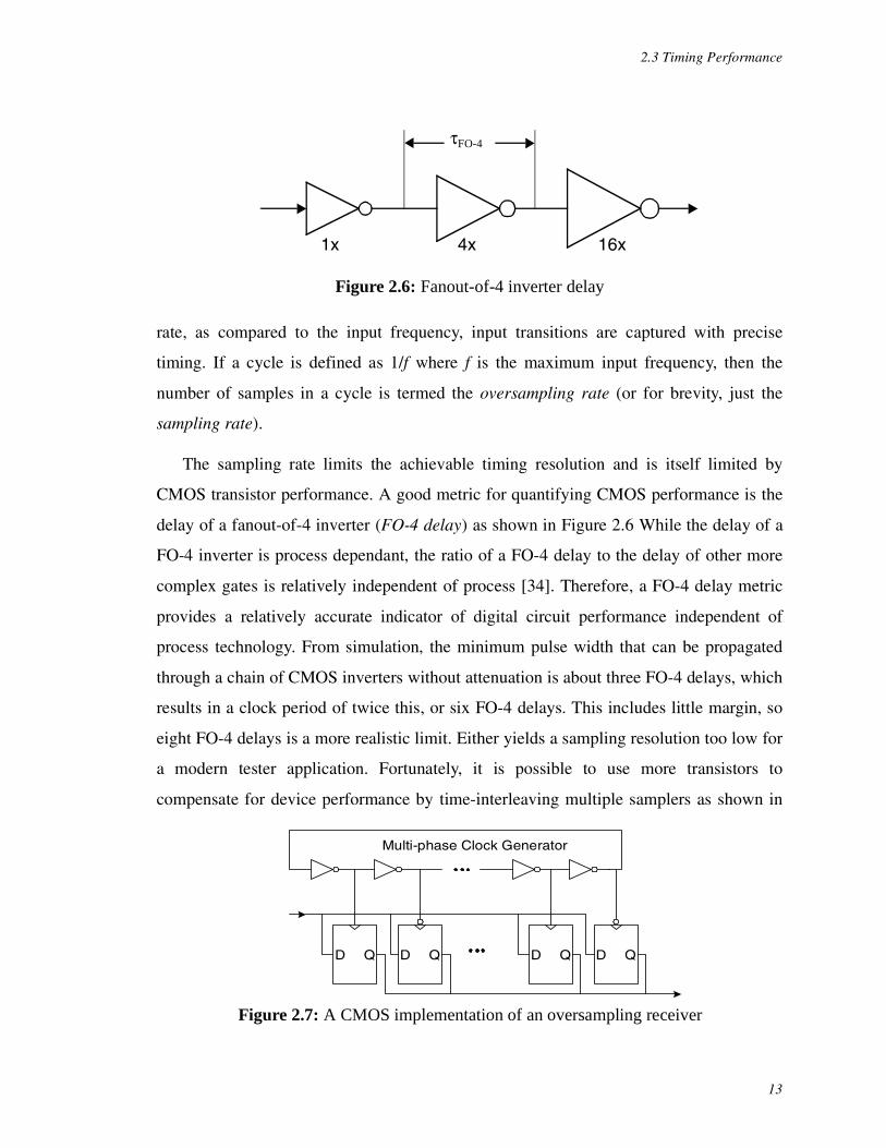
The sampling rate limits the achievable timing resolution and is itself limited by
CMOS transistor performance. A good metric for quantifying CMOS performance is the
delay of a fanout-of-4 inverter (FO-4 delay) as shown in Figure 2.6 While the delay of a
FO-4 inverter is process dependant, the ratio of a FO-4 delay to the delay of other more
complex gates is relatively independent of process [34]. Therefore, a FO-4 delay metric
provides a relatively accurate indicator of digital circuit performance independent of
process technology. From simulation, the minimum pulse width that can be propagated
through a chain of CMOS inverters without attenuation is about three FO-4 delays, which
results in a clock period of twice this, or six FO-4 delays. This includes little margin, so
eight FO-4 delays is a more realistic limit. Either yields a sampling resolution too low for
a modern tester application. Fortunately, it is possible to use more transistors to
compensate for device performance by time-interleaving multiple samplers as shown in
1x 4x 16x
Figure 2.6: Fanout-of-4 inverter delay
τFO-4
D Q D Q D QD Q
Multi-phase Clock Generator
Figure 2.7: A CMOS implementation of an oversampling receiver
2.3 Timing Performance
14
Figure 2.7. The set of time-interleaved flip-flops that samples the input is termed an input
channel. Multiple input channels can share a single clock generator to permit highly
integrated testers. This type of CMOS receiver has found previous application in high-
speed communication systems [36].
In an oversampled architecture, the sampling flip-flops can be clocked sense
amplifiers which allows the receiver to capture both low-swing and glitching input edge
transitions. The samplers generate a constant stream of data representing the state of the
input signal. While an oversampled receiver does not compress the output data as with a
time digitizer, it does has the advantage of generating data that is synchronous with
sampling clock. This can simplify the circuits required for acquisition and processing of
the data. The sampling frequency is set by the design of the oversampled receiver and is
independent of input signal transitions.
While an oversampled receiver can be used to capture input transition information and
serve as the basis for a tester input receiver, the timing accuracy limitations are not clear.
Chapter 3 explores how static phase offsets, jitter and input bandwidth restrictions limit
timing accuracy.

3.1 Multi-Phase Clock Generation
15
Chapter 3
Timing Accuracy
“In theory, there is no difference between theory and practice; In practice, there is”
- Chuck Reid
High-speed interfaces require testers with high timing accuracy. However, timing
accuracy in an oversampled receiver is limited by numerous error sources. To understand
the applicability of this technology to chip testing and to categorize the potential
performance, this chapter identifies and characterizes these error sources. Once this has
been done, compensation techniques are considered to yield an understanding of the
fundamental timing limitations.
This chapter starts by examining multi-phase clock generators since they are a
significant source of timing errors in an oversampled receiver. Sections 3.2 through 3.4
cover error sources within clock generators that limit timing resolution. Also presented are
measurement and calibration techniques to maximize timing performance in the presence
of error sources. The chapter ends with a discussion of the timing errors introduced by the
clocked sampling receivers.
3.1 Multi-Phase Clock GenerationThe discrete sampling nature of an oversampled receiver fundamentally limits the
achievable timing accuracy to ±τ/2 for a sample spacing of τ. Increasing the sampling
resolution requires high-frequency or finely spaced sampling clocks. The maximum
frequency of a clock generator is fundamentally limited by the ability to propagate clock
pulses through CMOS inverters which are the most basic form of a clock buffer. As
mentioned in Chapter 2, the minimum pulse width that can be propagated reliably without
attenuation is about four FO-4 delays which results in a clock period of twice this, or eight
FO-4 delays. This sets an absolute limit on the sampler clock frequency.1
3.1 Multi-Phase Clock Generation
16
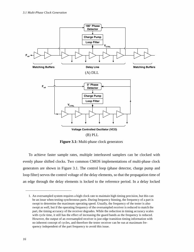
To achieve faster sample rates, multiple interleaved samplers can be clocked with
evenly phase shifted clocks. Two common CMOS implementations of multi-phase clock
generators are shown in Figure 3.1. The control loop (phase detector, charge pump and
loop filter) servos the control voltage of the delay elements, so that the propagation time of
an edge through the delay elements is locked to the reference period. In a delay locked
1. An oversampled system requires a high clock rate to maintain high timing precision, but this canbe an issue when testing synchronous parts. During frequency binning, the frequency of a part isswept to determine the maximum operating speed. Usually, the frequency of the tester is alsoswept as well, but if the operating frequency of the oversampled receiver is reduced to match thepart, the timing accuracy of the receiver degrades. While the reduction in timing accuracy scaleswith cycle time, it still has the effect of increasing the guard bands as the frequency is reduced.However, the output of an oversampled receiver is just edge transition timing information withno inherent concept of cycles, and therefore the tester receiver can be run at maximum fre-quency independent of the part frequency to avoid this issue.
180° PhaseDetector
Charge Pump
Loop Filter
Delay LineMatching Buffers
VCTRL
Matching Buffers
Fref
VCTRL
Fref
Voltage Controlled Oscillator (VCO)
0° PhaseDetector
Charge Pump
Loop Filter
Figure 3.1: Multi-phase clock generators
(A) DLL
(B) PLL
3.1 Multi-Phase Clock Generation
17
loop (DLL), the delay elements delay the incoming clock, while in a PLL, the delay
elements are connected in a ring to form a voltage controlled oscillator (VCO). By
matching the buffer elements that compose the delay line or VCO, multiple, uniformly
spaced clock phases are created. In Figure 3.1, the delay line is locked to only half the
period of the reference clock because differential buffers can generate the complementary
outputs. For single-ended delay elements, the number of delay elements in the delay line
can be doubled and locked to 360° rather than 180°. The matching buffers at the beginning
of the DLL pre-condition the input edge rate and signal swing so the first delay line buffer
has an identical input edge as the last buffer element. Those at the end equally load the last
buffer cell to reduce phase offsets.
In both the PLL and DLL, the spacing of the clock phases is limited to the minimum
propagation time through a delay element. If the loads on the DLL or PLL are much
smaller than the delay cells themselves, the minimum phase spacing can asymptotically
approach a FO-1 delay. While one might expect a FO-1 delay to be a quarter of a FO-4
delay, it is actually not quite that small. This is due to the additional self-loading of the
inverter diffusion capacitance. This capacitance is typically a factor of one-half to one of
the input gate capacitance. Therefore, a FO-1 delay is only 2-3 times smaller than a FO-4
delay, which, in a 0.25µm process, results in a FO-1 delay of roughly 50ps. Not only is
this larger than the resolution required to test a modern part, but it does not include a
mechanism to control the delay of the buffers. Delay tuning transistors or capacitors will
almost certainly increase the minimum delay. Finally, even if a FO-1 delay were
sufficient, there is no provision to increase the resolution (other than changing processes)
should it be required to do so in the future. So while this would enable a tester to scale
with process technology, it does not allow scaling at a rate faster than process technology.
What is needed is a technique to generate phase spacings that are a fraction of a gate delay.
Phase interpolation is an established technique for generating edges with finer timing
resolution compared to what can be achieved with individual buffers. This is
accomplished by blending two phase-shifted edges to produce a new edge that transitions
in between the existing edges. An interpolating element composed of two inverters is
shown in Figure 3.2. On the right side of the figure are three output waveforms. The top

3.2 Timing Accuracy
18
and bottom waveforms are the result of passing the two inputs through normal inverters.
The middle output waveform is created by shorting the outputs of two inverters together.
The result is a “smeared” output curve formed by the merged drivers.
Finely space clock edges can be generated by interpolating between coarsely spaced
clock edges created with a traditional clock generator, such a PLL or DLL. In theory,
interpolation can be recursively applied to create arbitrarily small phase spacings.
However, in practice, the achievable phase spacing is limited by numerous error sources
that are discussed in the following sections.
3.2 Timing AccuracyStatic and dynamic variations in the position of clock edges from their ideal locations
is a significant obstacle to building high-precision clock generators. Static variations,
termed static phase offsets, are clock edge placement errors caused by fixed error sources
such as device variations, circuit mismatches and layout asymmetries. Dynamic
variations, termed jitter, can be grouped into two categories: deterministic and random
[21]. Random jitter (RJ) is caused by fundamental noise sources in the clock generator
such flicker and thermal noise. Deterministic jitter (DJ) is caused by variations in the
clock edge due to deterministic and bounded sources, such as power supply noise.
∆T
Ain
Bin
Aout
Bout
Time averagedoutput
Figure 3.2: Interpolator operation
size=1
size=α
size=1
size=1-α
3.3 Static Phase Offsets
19
Deterministic error sources dominate on large digital chips, such as microprocessors, that
are the target environment of this work. For this reason, RJ is not considered further.1
3.3 Static Phase OffsetsGenerating precisely aligned clocks requires precise matching between the circuits
that produce and buffer each phase. However, device mismatch and physical limitations in
layout reduce this symmetry and therefore disturb the ideal phase alignment and produce
timing offsets. As the spacing between clock phases is reduced and becomes a small
fraction of a gate delay, static offset errors becomes a more significant fraction of the
timing resolution.
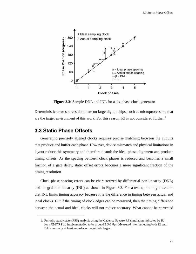
Clock phase spacing errors can be characterized by differential non-linearity (DNL)
and integral non-linearity (INL) as shown in Figure 3.3. For a tester, one might assume
that INL limits timing accuracy because it is the difference in timing between actual and
ideal clocks. But if the timing of clock edges can be measured, then the timing difference
between the actual and ideal clocks will not reduce accuracy. What cannot be corrected
1. Periodic steady state (PSS) analysis using the Cadence Spectre RF simulation indicates 3σ RJfor a CMOS PLL implementation to be around 1.3-1.8ps. Measured jitter including both RJ andDJ is normally at least an order or magnitude larger.
Figure 3.3: Sample DNL and INL for a six-phase clock generator
Ideal sampling clock
Actual sampling clock
Clock phases
Ph
ase
Po
siti
on
(d
egre
es)
0
60
120
180
240
300
0 1 2 3 4 5
β
α
γ
γ = INL
α = Ideal phase spacingβ = Actual phase spacingα−β = DNL

3.3 Static Phase Offsets
20
though, are DNL errors which are due to non-uniform spacing of the sampling clocks. In
the context of an oversampled receiver, the time between two clocks is termed a sampling
bin, and in places within this dissertation, abbreviated simply as bin.
It is interesting to note that DNL errors that result in smaller than expected bin sizes
will not introduce timing errors by themselves. In fact, timing accuracy is increased over
the part of the period where the edges are compressed, since the input edge position can be
determined with greater precision. However, a PLL or DLL control loop will drive the
sum of the DNL errors to zero and therefore, negative DNL errors implies the existence of
positive DNL errors which do reduce timing accuracy by increasing the size of the
corresponding sampling bin.
3.3.1 Sources of Static Phase Offset
A significant source of timing errors is device mismatch and asymmetries in circuits
and layout. These errors are not fundamental limitations, since device mismatch can be
reduced with larger devices and layout asymmetries can be reduced with multiple
fabrication trials, but they do present practical limitations. In all real designs, both
transistor sizes and design time are limited.
In both a DLL and a PLL, the control loop feedback clock increases the load on one of
the output phases. To maintain symmetry, dummy loads are used to balance loading on all
phases, but this requires additional area and power. DLLs have further circuit asymmetries
because of delay elements required at the ends to the delay line. The buffers at the end of
the DLL only cost area and power, but those at the beginning will contribute additional
jitter, as described in Section 3.4, because the reference clock edge must traverse through
these buffers before going through the delay line. Care must be taken to ensure changes
made to improve matching do not create additional jitter.
The layout of multi-phase clock generators, especially those with large numbers of
clocks is difficult because of matching and the resulting asymmetries are a significant
source of static phase offsets. First-order matching of layout capacitance is
straightforward, but matching second-order effects, such as coupling between active
signals is more challenging. Extraction tools can produce detailed models of the parasitic
3.3 Static Phase Offsets
21
capacitances, but the effect of coupling capacitances depends on the edge rate of the
coupling signals, which can change over process corners.
Static phase offsets are also caused by synchronous supply noise at the same
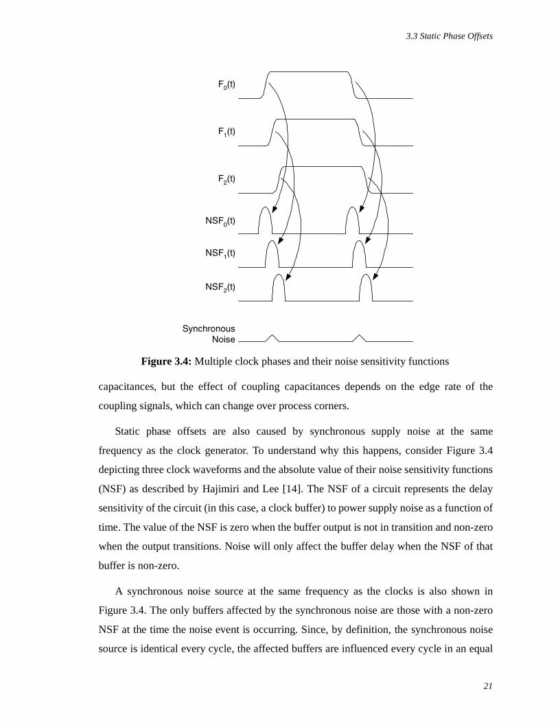
frequency as the clock generator. To understand why this happens, consider Figure 3.4
depicting three clock waveforms and the absolute value of their noise sensitivity functions
(NSF) as described by Hajimiri and Lee [14]. The NSF of a circuit represents the delay
sensitivity of the circuit (in this case, a clock buffer) to power supply noise as a function of
time. The value of the NSF is zero when the buffer output is not in transition and non-zero
when the output transitions. Noise will only affect the buffer delay when the NSF of that
buffer is non-zero.
A synchronous noise source at the same frequency as the clocks is also shown in
Figure 3.4. The only buffers affected by the synchronous noise are those with a non-zero
NSF at the time the noise event is occurring. Since, by definition, the synchronous noise
source is identical every cycle, the affected buffers are influenced every cycle in an equal
F0(t)
F1(t)
NSF0(t)
F2(t)
NSF1(t)
NSF2(t)
SynchronousNoise
Figure 3.4: Multiple clock phases and their noise sensitivity functions

3.3 Static Phase Offsets
22
manner and hence are consistently fast or slow depending on the nature of the noise
source. This assumes that the phase relationship between the synchronous noise and the
clocks is constant. If the alignment of the noise and the clock varies slowly (perhaps due to
temperature variations perhaps) then static offsets due to synchronous noise that are
measured and calibrated at start-up can re-manifest themselves as the temperature and
supply voltage of the part changes over time. If synchronous noise constitutes a large
fraction of the static phase offsets, calibration is more difficult since it must be run often
enough to the track changes in the noise characteristics. Fortunately, the effect of these
error sources need not be large and, at least for the design presented in Chapter 5, they are
not a significant issue.
3.3.2 Measurement and Calibration
Static phase errors are a significant source of timing errors, but can be reduced with
calibration. The position of the clock edges can be measured with averaged phase timing
measurements using histogram counters [18]. Given the static position of the clock
phases, static phase errors are removed by tuning adjustable interpolators within the clock
generators. The timing accuracy after calibration is limited by the resolution of the
interpolators. Published results have demonstrated interpolators that can be adjusted over
a range of a FO-4 delay with 4 bits of resolution and a DNL of less than one LSB (1/16 of
a FO-4) [30].
Averaged phase timing measurements do not limit the achievable timing accuracy
provided they are performed over sufficiently long periods so that dynamic errors due to
jitter average to zero. The measurement is performed by sampling a random signal with
the multiple clock phases, as shown in Figure 3.5. Histogram counters record the number
of input transitions between adjacent samplers. An additional counter limits the
acquisition period by counting system cycles. If the input signal edges are randomly
distributed within the cycle and the sampling clock edges are evenly spaced, then the
histogram counters will have identical values. If the sampling clocks are unevenly spaced
due to static phase errors, the counters will not be equal and the difference will be
proportional to the phase spacing error.
3.3 Static Phase Offsets
23
Input transitions are detected within sampling bins when the XOR of two adjacent
sampler outputs is a logical one. While a random input signal is sufficient, it is useful to
consider the desired characteristics of the input signal with more detail. The frequency of
the input signal must be constrained so that it evenly cycles through the sampling bins. For
instance, if the input signal is the same frequency as the clock generator, the input
transitions will not cycle through all the bins and an accurate histogram cannot be
measured. If the input signal has a period that is two-thirds of the clock generator, then the
input edge placement will repeat every 3 cycles. To ensure that quantization noise in the
measurement does not limit calibration, the input signal must be constrained such that,
Fsys is frequency of the clock generatorFinp is the frequency of the input signal
Tbin is the resolution of a binTadj is the resolution of a LSB
Random Input
Sampling Clocks
Edge Detect
Hit Counters
Sampled Data
Figure 3.5: Histogram measurement of static clock phase alignment
LeastCommonMultiple Fsys Finp,( )Fsys
----------------------------------------------------------------------------------------- BinCountTbin
Tadj
--------- .⋅>
3.4 Deterministic Jitter
24
This implication of this equation is that there must be enough unique input edges
within a cycle so that the measurement resolution is at least as large as the resolution of
the interpolation adjustment. Otherwise, the interpolator would be able to move an edge
with greater resolution than could be measured. Sampling clock jitter does not affect this
measurement because it is just as likely to make a sampling bin smaller than larger and
thus averages out for a sufficiently large histogram period. Sampler input offsets will skew
the histogram measurements and need to be minimized before this measurement technique
is used.
Given the ability to position to a clock edge within 1/16 of a FO-4 delay [31] and
measure the timing of clock edges to an arbitrary precision [17], it appears possible to
constrain phase errors to within about 3% of a FO-4 delay. This is significantly better than
previously reported data for multi-phase clock generators. Maneatis in [23] reports DNL
phase spacing errors of 14.3% of a FO-4 delay in a 2µm process and Yang reports similar
DNL measurements in [37] for uncompensated clock generators. Potentially even more
important however, is the robustness of the technique as unexpectedly large static phase
offsets are a reoccurring theme found in many papers that report DNL measurement for
multi-phase clock generators [6][23][37]. Even the test chip presented in Chapter 5 had
larger than expected phase errors due to matching issues within the DLL that went
unnoticed during the initial design. With sufficient adjustment range, even large
unexpected errors can be compensated rather than requiring a redesign, new masks and the
associated manufacturing delay. Given that static phase offsets can be controlled, system
performance will then be limited by jitter which is described next.
3.4 Deterministic JitterDeterministic jitter is caused by variations in the propagation time of delay elements
and clock buffers. It is caused by noise modulating the delay of clock buffers and delay
elements and limits the timing accuracy of an oversampled receiver by introducing timing
uncertainty in the acquired data. The delay sensitivity of a circuit to supply noise can be
quantified as:
Power Supply Delay Sensitivity% change in delay
% change in power supply---------------------------------------------------------------.=
3.4 Deterministic Jitter
25
Jitter can be reduced by decreasing the supply sensitivity of the clock generator. This
has been the focus of much research and the result is delay elements with a supply
sensitivity that is more than an order of magnitude better than a CMOS inverter [25].
Unfortunately, clock buffers are still generally built with CMOS inverters. Jitter
introduced by the clock buffers is a significant limitation to achieving low-jitter sampling
clocks in a multi-channel oversampled receiver because long clock chains are required to
drive the large clock loads.
Power supply noise is typically the dominant source of jitter in CMOS parts primarily
because the circuit styles and architectures currently employed have large transient current
variations. CMOS logic draws little or no power when idle, but large currents when
switching. Furthermore, the common practice of aggressive clock gating in modern parts
to conserve power can cause significant current spikes. Current transients combine with
the inductance and resistance of the power supply network to produce voltage fluctuations
that ripple through the supply network. This problem is becoming more severe with each
generation of VLSI parts as the supply voltage is trending downward, but the dissipated
power is remaining relatively constant. Therefore, the required supply current and
associated dI/dt spikes are increasing.
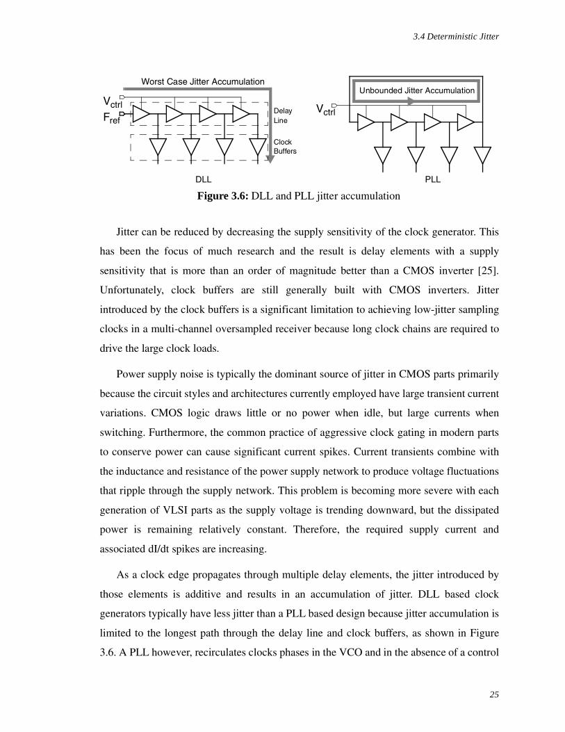
As a clock edge propagates through multiple delay elements, the jitter introduced by
those elements is additive and results in an accumulation of jitter. DLL based clock
generators typically have less jitter than a PLL based design because jitter accumulation is
limited to the longest path through the delay line and clock buffers, as shown in Figure
3.6. A PLL however, recirculates clocks phases in the VCO and in the absence of a control
Fref
Worst Case Jitter Accumulation
DLL
VctrlVctrl
Unbounded Jitter Accumulation
PLL
DelayLine
ClockBuffers
Figure 3.6: DLL and PLL jitter accumulation

3.4 Deterministic Jitter
26
loop, jitter accumulation is unbounded. Given a control loop, the jitter accumulation in the
VCO is bounded, but even under optimistic conditions, it is still about six times the peak
of a delay line [32]. In practice however, such a major discrepancy in jitter performance
does not exist because, as described in the previous section, the noise sensitivity of the
delay elements is much better than that of the clock buffers.
Jitter can be quantified as either absolute or cycle-to-cycle. Absolute jitter is the
difference between an ideal clock edge and the actual edge, while cycle-to-cycle jitter is
the difference between clock periods. In some applications, such as microprocessors,
absolute jitter is unimportant because there is no other internal timing reference. For such
applications though, cycle-to-cycle jitter is important because it requires adding timing
margin to logic circuits to ensure that the results is properly clocked into the following
latches or flip-flops. For chip testers absolute jitter is important since the part being tested
may contain a PLL or other type of VCO structure that does not track absolute jitter in the
tester. The only time base that the two systems have in common is real time and therefore,
absolute jitter cannot be ignored.
3.4.1 Measurement and Compensation
Both cycle-to-cycle and absolute jitter can be measured by sampling an externally
generated reference clock with an input channel. If the reference has low-jitter relative to
the sampling system clock generator, any jitter in the measured position of the reference
clock can be attributed to the sampling system.1 If this jitter is correlated between
channels, then the jitter measurement from one channel can be used to compensate
sampled data from the other channels. While the achievable degree of correlation between
channels is not clear, it is reasonable to assume that if the principal source of jitter is the
clock generator and drivers, a design that has a minimum of local clock buffering in each
channel might have a high degree of correlation in jitter between channels. Data
supporting this assumption is presented in the next chapter.
1. External crystal and hybrid SAW oscillators with only a few picoseconds rms jitter are availablefrom Vectron International and other suppliers.

3.5 Input Samplers
27
The bandwidth of the jitter can limit the effectiveness of the compensation. Because
the jitter is sampled once a cycle (or twice if both edges of the reference clock are
measured), we know by Nyquist’s theorem that the maximum frequency that can be
measured is one-half the reference clock frequency. Jitter at higher frequencies is aliased
down to lower frequencies by the sampling operation and appears as noise in the jitter
measurement. The size of the error is determined by the frequency of the reference clock
and the power spectrum of the jitter. Fortunately, this does not need to be a significant
source of error because high-frequency (multi-GHz) reference clocks can be used in
conjunction with the liberal application of on-chip bypass capacitance which limits high
frequency noise.
3.5 Input SamplersHaving described a technique for generating and measuring the multi-phase clocks,
this section explores the issues with input sampler design. A model for an ideal input
sampler is shown in Figure 3.7. The input switches are toggled every cycle to
instantaneously capture the state of the input signal. The amplifier permits the digital latch
to resolve arbitrarily small differences in the sampled inputs. Unfortunately, physically
realizable samplers have many non-idealities, not modeled in Figure 3.7, which introduce
timing errors.
Device mismatch in both the input switches and amplifier is significant sampler
limitation in an oversampled receiver. Mismatch results is a non-zero differential
amplifier output for a zero volt differential input. The input voltage that causes a zero
differential output voltage is termed the input referred offset voltage and can be modeled
as a random, but static, error source added to the input signal.
A
nT
Input Latch
Figure 3.7: Ideal input sampler

3.5 Input Samplers
28
The amplifier has a limited gain-bandwidth product and for small input signals, the
amplifier may lack the required gain to overwrite the data latch or storage elements that
follow. This introduces hysteresis into the system. However, gain can be increased at the
expense of an additional pipeline delay. For this reason, hysteresis in the data latch is not a
limiting factor. A model of the input sampler with these effects is shown in Figure 3.8.
A further limitation is the finite bandwidth of the sampling operation. Thus, rather
than instantaneously sampling the input signal, the sampler takes a weighted average of
the input signal over a finite window in time. The shape of the window depends on both
the edge rate of the clocks and type of circuit used. The weighting function is termed the
sampling impulse or aperture function and represents the period over which the sampler is
sensitive to the input signal. The minimum width of this curve that includes 50% of the
area is termed the sampling aperture. The sampling aperture is a useful metric because it
specifies the minimum input pulse width that can be captured by the sampler. While
described in the time domain, the aperture can also be modeled in the frequency domain as
a low-pass filter preceding ideal input switches. All sampling amplifiers have a finite
aperture even if they do not have explicit sampling switches. In addition to the input filter
due to the sampling impulse, an additional filter exists, formed by the input source
resistance and the capacitive load of the sampler inputs. The signal must flow through this
low-pass RC filter before it appears at the input of the samplers. Hence, the effective filter
is a cascade of the two.
The sampler input filter distorts the shape of the DUT output waveform and can create
a static timing error. Prior to test, the delay between the tester and the DUT (due to the test
socket, load board and tester cables) is measured so that it can be subtracted from the
actual test measurements. Because of the filtering due to the input samplers, the
nT
HS(s) A HA(s)HF(s)
Figure 3.8: Differential input receiver with non-idealities
Input RC Sampling Ideal Regeneration LatchFilter Aperture Amplification Time Constant Hysteresis Latch
S
RQ
Data

3.5 Input Samplers
29
magnitude of the delay depends on the threshold voltage of the input receiver. Testing a
part at a threshold voltage different from the threshold used for calibration results in a
static timing error.1 Higher input bandwidths filter the signal less and result in lower
timing errors. The interconnect between the DUT and tester will also filter the input so
extending the input bandwidth of the sampler significantly past the bandwidth of the
interconnect yields diminishing returns.2
The input filter is dominated by the input capacitance of the samplers rather than the
aperture. An aperture of about 1/4 of a FO-4 delay can be achieved in a modern VLSI
processes and results in a very high -3dB frequency [37]. The input capacitance can be
quite significant a large number of samplers are connected to the input in an interleaved
oversampled receiver. The timing error due to input filtering can only be reduced by
increasing the -3dB frequency of the filter. Unfortunately, the source impedance is usually
fixed at 50Ω, or thereabouts,3 and thus the only way to increase the -3dB frequency is to
reduce the capacitive loading. In some cases, such as the experimental test chip described
in Chapter 4, the input capacitance is dominated by ESD protection devices. However, the
inputs of embedded testers only sample signals within the die and do not need ESD
protection. Therefore, reducing the input capacitance of the samplers and associated wire
loading is vital to maintain high timing accuracy.
Reducing the capacitive loading of a sampler requires small input devices.
Unfortunately, transistor mismatch is inversely proportional to the square root of the
device area. As the devices are made smaller to reduce capacitive loading, the input offset
voltage of the sampler increases. The input offset results in a timing error dependant on
the input signal slew rate, as shown in Figure 3.9. For signals with a high-slew rate, the
effective error due to a given offset voltage is less than for a signal with a slower slew rate.
1. Sweeping the input receiver threshold voltage allows the creation of a shmoo plot of the inputsignal.
2. For this reason, and to minimize TDR errors, it is beneficial to build a tester load board withhigh-quality printed circuit board material with low dielectric loss even if the part being tested isintended for use with a lower quality PCB material.
3. Or 25Ω for lines with double termination.
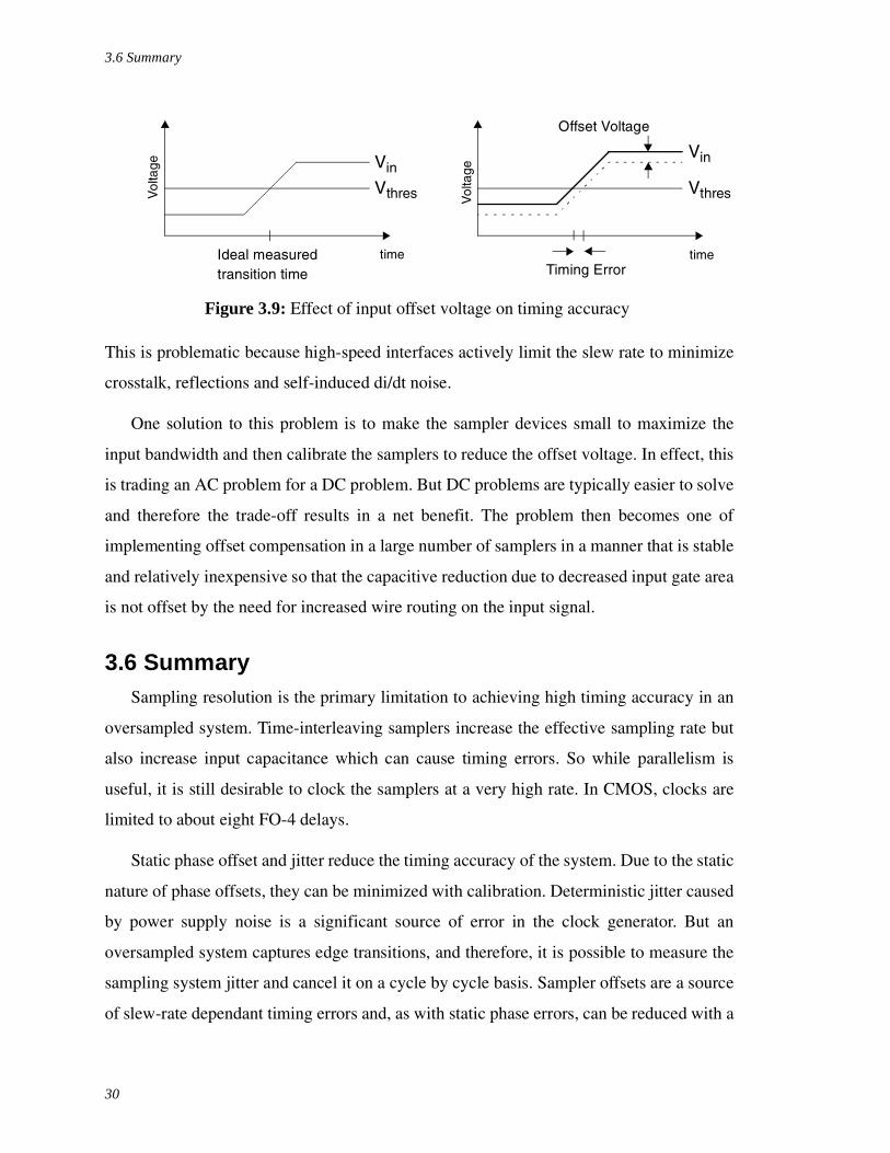
3.6 Summary
30
This is problematic because high-speed interfaces actively limit the slew rate to minimize
crosstalk, reflections and self-induced di/dt noise.
One solution to this problem is to make the sampler devices small to maximize the
input bandwidth and then calibrate the samplers to reduce the offset voltage. In effect, this
is trading an AC problem for a DC problem. But DC problems are typically easier to solve
and therefore the trade-off results in a net benefit. The problem then becomes one of
implementing offset compensation in a large number of samplers in a manner that is stable
and relatively inexpensive so that the capacitive reduction due to decreased input gate area
is not offset by the need for increased wire routing on the input signal.
3.6 SummarySampling resolution is the primary limitation to achieving high timing accuracy in an
oversampled system. Time-interleaving samplers increase the effective sampling rate but
also increase input capacitance which can cause timing errors. So while parallelism is
useful, it is still desirable to clock the samplers at a very high rate. In CMOS, clocks are
limited to about eight FO-4 delays.
Static phase offset and jitter reduce the timing accuracy of the system. Due to the static
nature of phase offsets, they can be minimized with calibration. Deterministic jitter caused
by power supply noise is a significant source of error in the clock generator. But an
oversampled system captures edge transitions, and therefore, it is possible to measure the
sampling system jitter and cancel it on a cycle by cycle basis. Sampler offsets are a source
of slew-rate dependant timing errors and, as with static phase errors, can be reduced with a
Vthres
Vin
Ideal measuredtransition time
Vthres
Vin
Timing Errortime
Vol
tage
Vol
tage
time
Offset Voltage
Figure 3.9: Effect of input offset voltage on timing accuracy
3.6 Summary
31
calibration sequence performed prior to operation. The next chapter details a test chip built
to investigate the trade-offs and issues encountered when implementing these techniques
along. The chapter also includes test measurements to determine the achievable timing
accuracy.

3.6 Summary
32

4.1 Test Chip
33
Chapter 4
Implementation and Timing Peformance
“I have not failed 10,000 times. I have successfully found 10,000 ways that will not work”
- Thomas Edison
The previous chapter examined implementation independent timing issues in an
oversampled system. This chapter describes oversampled input receiver implementation
details and measured lab results. The first section of this chapter provides an overview of
the sampling system included on the test chip. The timing accuracy is primarily limited by
the clock generators which are described in Section 4.2. This includes interpolation
circuits for creating finely spaced clocks and architectural trade-offs for building multi-
phase clock generators with tunable output phases. The section concludes with test results
for static phase and jitter compensation techniques for two clock generators. Having
explored methods to build clock generators, Section 4.3 then examines clocked input
samplers that can capture high-speed signals while having a minimal impact on timing
accuracy.
4.1 Test ChipTo better understand the trade-offs described in the previous chapter, and to test the
compensation methods, a sampling receiver test chip was designed and measured. A block
diagram of the test chip is shown in Figure 4.1. The part was fabricated in a standard
0.25µm, five metal layer process. It contains eight sampling channels that feed either an
SRAM memory or an on-chip histogram counter. The sampling rate per channel is
36Gsamples/s with a 900MHz reference clock and 40 sampling phases. The eight
sampling channels generate 288Gb/s of digital data but to reduce the required bandwidth
of the acquisition memory, the data rate is reduced by oversampling only half the cycle.
The memory is capable of storing the resulting 144Gb/s data stream with no further loss of
information. The chip contains two circuits that can be used to generate the finely spaced
(27ps) clocks. One uses a delay line with interpolation and the other uses an array of

4.2 Clock Generation
34
oscillators. Since the clock generators are the most critical circuits, they are discussed
next.
4.2 Clock GenerationThe clock generators drive the input sampling receivers and set the timing of the entire
system. To compare design trade-offs and performance, both a phase-locked loop and
delay-locked loop were included on the test chip. The performance of the delay elements
in the clock generators significantly impacts the jitter performance, so this section starts
with a description of a low-jitter differential delay element. The delay element is then
transformed into a tunable interpolator to permit fine phase spacing. The section continues
with a discussion of the issues involving the incorporation of tunable interpolators into a
delay line and VCO to achieve a large adjustment range without compromising
performance. The control loops and clock buffers are then described along with
techniques to minimize the static phase offsets and jitter caused by these elements.
4.2.1 Basic Elements
The clock generators are implemented with Maneatis style self-biased control loops
and replica biased, variable delay, differential buffers with symmetric loads [25]. A buffer
is shown in Figure 4.2. The two PMOS devices that form the load structures are termed
symmetric loads in [23]. If the output swing is equal to the bias voltage Vbp, then the
resistance of the loads is symmetric about the crossing of the differential outputs. This
Input[7:0]
0 1 19x8
Array oscillator
DLL
φ
Sync D/C
900MHz
160 320
450MHz
320x128SRAM
20b histogram
20b histogramφ2
FSM Testb
us
Figure 4.1: Test chip block diagram

4.2 Clock Generation
35
reduces the jitter caused by common-mode supply noise. Vbp is driven by the control loop,
described in section 5.2.4, to set the delay of the buffer. Vbn is dynamically set by the
replica biasing circuit in Figure 4.3 to set the output signal swing equal to Vbp which
maintains the symmetric nature of the loads. The differential topology, symmetric loads,
and replica biasing yields a delay element with a low sensitivity to supply noise. A
standard inverter has a delay sensitivity of roughly 1, while this element has a delay
sensitivity of about 0.05, which is an improvement by a factor of twenty.1
Vdd Vdd
GND
Vbn
Vbp
A
X
M1 M2 M3 M4
M5M6
M7
A
X
Figure 4.2: Differential delay element
Vdd
GND
Vbn
VbpM1 M2
M3
M4
Vdd
+-
Figure 4.3: Replica bias generator for delay elements

4.2 Clock Generation
36
An interpolator can be built with two differential buffers by shorting their outputs
together, as shown in Figure 4.4 [23]. In this figure, the PMOS loads from the two buffers
have been merged and the A and B inputs are the clocks being interpolated. The output
phase is set by the relative strengths of the two sides. While ideally all devices in the
buffers should be scaled to change the output phase, only the size of the current source
devices, M9 and M10, really matter. To maintain constant signal swings, the sum of the
currents in the two current sources must remain constant.
In previously published multi-phase clock generators, current sources M9 and M10
were fixed to a value that optimized the simulated phase spacing [37]. On the test chip, the
current sources are implemented as 3-bit current DACs, as shown in Figure 4.5, to permit
run-time adjustment of the clock phases. This adjustment allows for correction of small
static errors in the clock phases. The DAC is binary rather than thermometer encoded
because monotonicity is not required.1 Standard matching techniques are used to layout
1. Recall delay sensitivity, as defined in Chapter 3, is the percent change in delay divided by thepercent change in supply voltage and is unitless.
1. Previous application of the adjustable interpolators use a thermometer coded DAC to permitdynamic changes to the current weights [31]. However, for this application, the adjustmentcodes are only changed during an initial calibration sequence so less complex binary weightingis instead used. The DAC currents do not even have to be monotonic as the calibration algorithmcan check all possible adjustment codes and pick the best one.
Vdd Vdd
GND
Vbn
Vbp
A B
X
M1 M2 M3 M4
M5 M6 M7 M8
M9 M10
BA
X
Figure 4.4: Differential interpolator
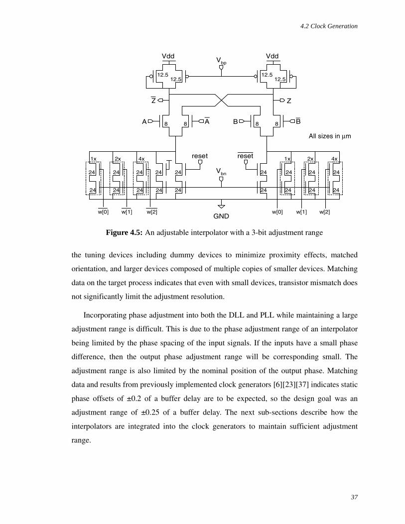
4.2 Clock Generation
37
the tuning devices including dummy devices to minimize proximity effects, matched
orientation, and larger devices composed of multiple copies of smaller devices. Matching
data on the target process indicates that even with small devices, transistor mismatch does
not significantly limit the adjustment resolution.
Incorporating phase adjustment into both the DLL and PLL while maintaining a large
adjustment range is difficult. This is due to the phase adjustment range of an interpolator
being limited by the phase spacing of the input signals. If the inputs have a small phase
difference, then the output phase adjustment range will be corresponding small. The
adjustment range is also limited by the nominal position of the output phase. Matching
data and results from previously implemented clock generators [6][23][37] indicates static
phase offsets of ±0.2 of a buffer delay are to be expected, so the design goal was an
adjustment range of ±0.25 of a buffer delay. The next sub-sections describe how the
interpolators are integrated into the clock generators to maintain sufficient adjustment
range.
Vdd Vdd
GND
Vbn
Vbp
A B
Z
24
24
24
24
24
12.512.5
12.512.5
8 8 88
reset
2424
24
24
24
24
24
1x 2x 4x
w[0] w[1]
A
Z
w[2]
B
reset
24
24
1x
w[0]
24
24
2x
w[1]
24
24
4x
w[2]
Figure 4.5: An adjustable interpolator with a 3-bit adjustment range
All sizes in µm
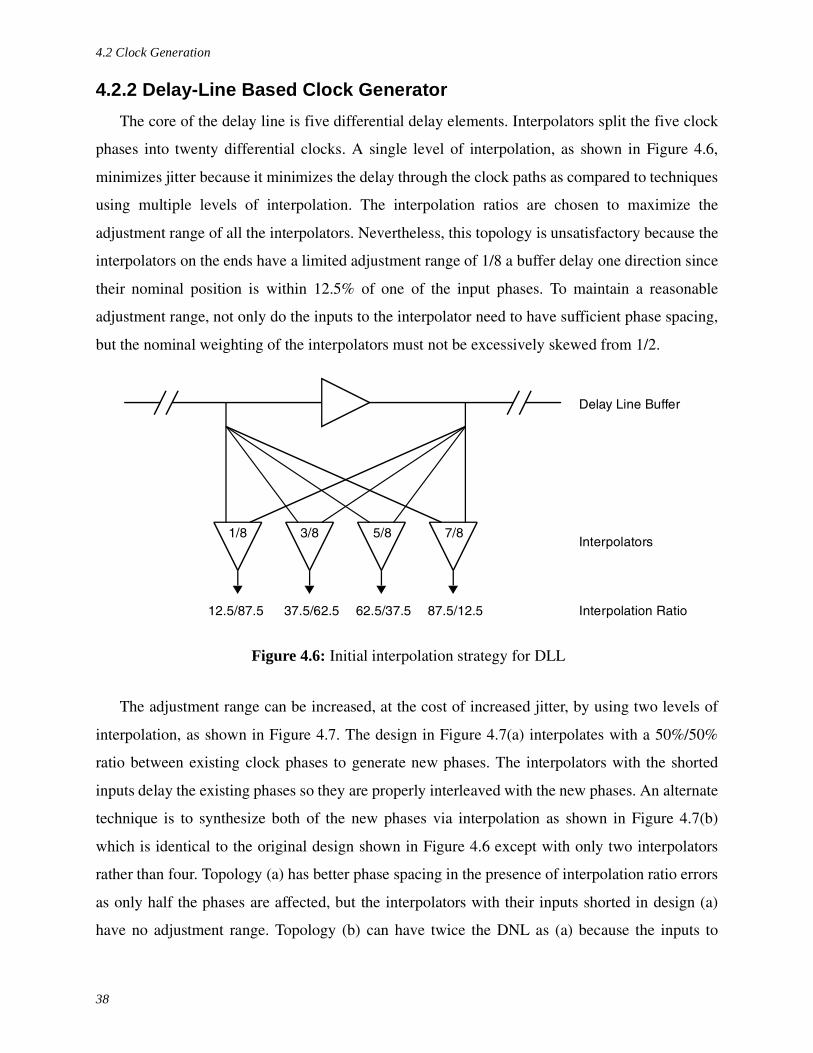
4.2 Clock Generation
38
4.2.2 Delay-Line Based Clock Generator
The core of the delay line is five differential delay elements. Interpolators split the five clock
phases into twenty differential clocks. A single level of interpolation, as shown in Figure 4.6,
minimizes jitter because it minimizes the delay through the clock paths as compared to techniques
using multiple levels of interpolation. The interpolation ratios are chosen to maximize the
adjustment range of all the interpolators. Nevertheless, this topology is unsatisfactory because the
interpolators on the ends have a limited adjustment range of 1/8 a buffer delay one direction since
their nominal position is within 12.5% of one of the input phases. To maintain a reasonable
adjustment range, not only do the inputs to the interpolator need to have sufficient phase spacing,
but the nominal weighting of the interpolators must not be excessively skewed from 1/2.
The adjustment range can be increased, at the cost of increased jitter, by using two levels of
interpolation, as shown in Figure 4.7. The design in Figure 4.7(a) interpolates with a 50%/50%
ratio between existing clock phases to generate new phases. The interpolators with the shorted
inputs delay the existing phases so they are properly interleaved with the new phases. An alternate
technique is to synthesize both of the new phases via interpolation as shown in Figure 4.7(b)
which is identical to the original design shown in Figure 4.6 except with only two interpolators
rather than four. Topology (a) has better phase spacing in the presence of interpolation ratio errors
as only half the phases are affected, but the interpolators with their inputs shorted in design (a)
have no adjustment range. Topology (b) can have twice the DNL as (a) because the inputs to
12.5/87.5 37.5/62.5 62.5/37.5 87.5/12.5 Interpolation Ratio
Delay Line Buffer
Interpolators
Figure 4.6: Initial interpolation strategy for DLL
1/8 3/8 5/8 7/8

4.2 Clock Generation
39
every other interpolators are reversed so adjacent phases are pushed in opposite directions.
However, the interpolators in (b) do have a larger adjustment range of at least 0.25 of a
FO-4 delay.
For a two-level DLL, the first level of interpolators need not be adjustable. It is
sufficient that the phases in the second level are tunable. Thus, the interpolation topology
in Figure 4.7(a) is used for the first level. It was initially assumed that the second level
could be the topology shown in Figure 4.7(b). But this results in a phase adjustment range
of only 12.5% of a FO-4 delay since the input clocks to the second level interpolators are
spaced by half a buffer delay rather than a full buffer delay as in the case of the first level
interpolators. The result is that rather than having an adjustment range of 25% of a buffer
delay, the interpolators in the second level only have an adjustment range of half that, or
12.5%, which again is unsatisfactory.
The solution for the second level is to interpolate between every other input clock
rather than adjacent clocks. The increased phase spacing does not cause adjustment
linearity problems with the interpolators because every other clock is spaced apart by one
buffer delay. The resulting interpolation topology is shown in Figure 4.8. An added benefit
is that because of the interleaved interpolation in the second level, the interpolation ratio is
37.5/62.5, which results in a reasonably good range. Because of device size quantization
due to the layout tool used, the final ratio was 36/64 which resulted in a built-in DNL of
3% of a FO-4 delay, or about 4ps.
25/75 75/2550/50 50/50 50/50
(a) (b)
Figure 4.7: Interconnect techniques for phase interpolation
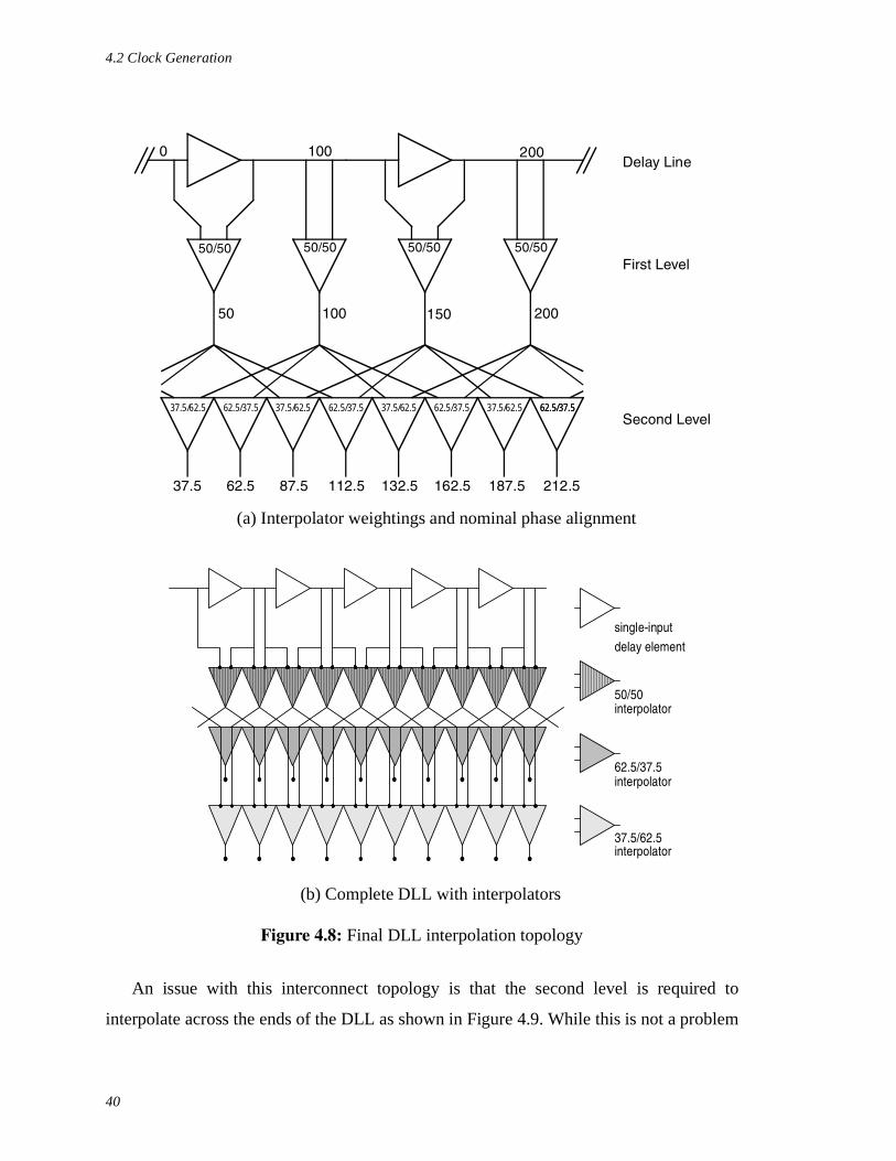
4.2 Clock Generation
40
An issue with this interconnect topology is that the second level is required to
interpolate across the ends of the DLL as shown in Figure 4.9. While this is not a problem
0 100 200
50 100 150 200
87.5 112.5 132.5 162.5 187.562.537.5 212.5
50/50 50/50 50/50 50/50
37.5/62.5 37.5/62.5 37.5/62.5 37.5/62.562.5/37.5 62.5/37.5 62.5/37.5 62.5/37.562.5/37.5
Delay Line
First Level
Second Level
single-input
delay element
62.5/37.5interpolator
37.5/62.5interpolator
50/50interpolator
(a) Interpolator weightings and nominal phase alignment
(b) Complete DLL with interpolators
Figure 4.8: Final DLL interpolation topology

4.2 Clock Generation
41
if the delay is exactly 180°, it is usually slightly off because of mismatch in other elements
in the feedback control loop, specifically the charge pump. Most of the interpolators in the
second level see a fraction of this error as it is spread evenly across them. However, the
interpolators that interpolate across the ends of the delay line see the entire error which
results in a large offset error for these phases. This is a common problem in DLLs and was
expected, but it was also expected that the interpolator adjustment range would be
sufficient to correct it. The adjustment range was unfortunately was not sufficient, as data
presented in the following sections demonstrates.
Increasing the interpolator adjustment range solves this problem but is costly because
additional adjustment range is added to all the interpolators despite only those on the ends
of the DLL requiring it. A potentially better solution is to include an adjustable current
DAC on the control line of the DLL. The DAC can be programmed to add or remove
sufficient current to compensate for offset errors in the control loop and would directly
correct the observed problem.1
4.2.3 Ring Oscillator Based Clock Generator
The previously described interpolation techniques are also applicable to a
conventional ring oscillator based VCO. Yang describes such a clock generator in [36]
1. Two issues with such a solution are the offset of the phase detector used to drive the loop con-trolling the DAC, as this will cause an uncompensated timing error, and the need to generate avery small correction current with the DAC. Neither appear to be significant obstacles, but theperformance of these circuits will limit the achievable duty-cycle.
Figure 4.9: DLL interconnect wrap aroundwrap-around

4.2 Clock Generation
42
with 24 phases for over-sampling a 2.5 Gb/s SONET signal. However, given the need for
interpolation, possibly a more interesting architecture is the array oscillator as described
by Maneatis in [23]. This structure uses multiple, coupled ring oscillators to create equally
phase shifted clocks.
To those unfamiliar with an array oscillator, the operation can be confusing so it is
briefly reviewed before proceeding with the details of adding phase tuning to the structure.
First, consider a series of uncoupled ring oscillators as shown in Figure 4.10. In an ideal
environment, the ring oscillators will oscillate with identical frequencies, but with an
arbitrary phase alignment. While this produces multiple output clocks, the arbitrary phase
alignment of the clocks makes this solution uninteresting. To generate equally spaced
output clocks, a forced phase alignment between the rings is required. This can be
achieved by replacing each of the single input buffers with a two-input interpolator and
coupling the rings together. The second input to the interpolator is derived from the
adjacent clock ring as shown in Figure 4.11.
In this configuration, the top and bottom rings are left uncoupled. The minimum
energy point of the system occurs when the input to the interpolators arrive at the same
time and hence the rings will oscillate in phase and multiple clocks will have the same
phase offset.
A phase shift can be forced between the rings by coupling the top and bottom rings as
shown in Figure 4.12. The symmetry of the design yields many favorable characteristics.
The phase shift is spread evenly between the rings to create equally spaced sampling
Figure 4.10: Multiple, uncoupled ring oscillators
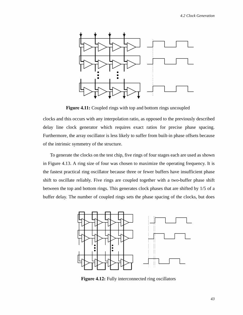
4.2 Clock Generation
43
clocks and this occurs with any interpolation ratio, as opposed to the previously described
delay line clock generator which requires exact ratios for precise phase spacing.
Furthermore, the array oscillator is less likely to suffer from built-in phase offsets because
of the intrinsic symmetry of the structure.
To generate the clocks on the test chip, five rings of four stages each are used as shown
in Figure 4.13. A ring size of four was chosen to maximize the operating frequency. It is
the fastest practical ring oscillator because three or fewer buffers have insufficient phase
shift to oscillate reliably. Five rings are coupled together with a two-buffer phase shift
between the top and bottom rings. This generates clock phases that are shifted by 1/5 of a
buffer delay. The number of coupled rings sets the phase spacing of the clocks, but does
Figure 4.11: Coupled rings with top and bottom rings uncoupled
Figure 4.12: Fully interconnected ring oscillators

4.2 Clock Generation
44
not affect the maximum oscillation frequency of the array. In fact, additional rings can
increase the frequency of oscillation because as more rings are added, the phase shift
between interpolator inputs is reduced which decreases the interpolator delay. While a two
buffer phase shift limits the maximum frequency of operation, it is required to allow the
integration of static phase tuning, as is described in the next section.
Adjustable Interpolation
Maintaining a large phase adjustment range in the array oscillator is a challenge as it is
with the delay line, but for a different reason. Phase adjustment in the delay line is difficult
because some of the interpolators have limited range due to an asymmetric interpolation
ratio. With the array however, the interpolators all can be designed to have 50/50 ratio so
the adjustment has sufficient range in both directions. But the phase difference between
0 5 10
18 3 8 13
16 1 6 11
14 19 4 9
12 17 2 7
15
17 2 7 12
denotes cross of differential pairs
Figure 4.13: Four by five array oscillator

4.2 Clock Generation
45
the inputs to the interpolator is set by the coupling between the first and last rings in the
array. If a one buffer phase shift is forced between the rings, then that delay will be spread
evenly across the rings and the inputs to the interpolators will have a phase difference of 1/
N times a buffer delay, where N is the number of coupled ring oscillators.
On the test chip, N=5 so the inputs would be spaced 22ps. But because the adjustment
range of an interpolator is set by the phase spacing of the inputs, the adjustment range of
the outputs is limited to only +/-11ps, which is insufficient to fully correct for the expected
offset errors.1 Therefore, increasing the array coupling factor to 2 increases the adjustment
range to 44ps (+/-22ps). However, this comes at the expense of reducing the maximum
oscillation frequency due to increased interpolator delay.
Because of coupling, adjusting a single phase in the array shifts all the phases.
Therefore, array calibration is more complex than with the DLL, where phases can be
independently adjusted. However, the output of the interpolator being tuned exhibits the
largest change. Hence, convergence is assured using an iterative calibration algorithm.
Incorporating adjustment into the array oscillator has an addional benefit besides
phase tuning: the adjustment devices can be used to reset the array. This is important
because the boundary conditions established by the ring coupling can be satisfied by
multiple stable modes. If the rings are coupled with a single buffer delay, then a one-buffer
delay phase shift would satisfy the boundary conditions, in addition to a phase shift of one
cycle plus one buffer delay. For normal operation, the state with the maximum operating
frequency is desired, but in both simulation and laboratory testing, the array sometimes
resets into a slower mode. The rings can be uncoupled using the adjustment devices and
the resulting series of stand-alone ring oscillators will oscillate at a frequency higher than
that of a coupled array.2 As the coupling is re-enabled, the ring oscillation frequency is
reduced slightly and the array enters into the desired mode. In the laboratory this proved to
be a very effective way to reset the array oscillator.
1. Mismatch in wire delay alone causes an error close to this value.2. Provided the coupling factor is positive. It is possible to couple the array with a negative factor
and actually cause it to oscillate at a frequency higher than a standalone ring oscillator.
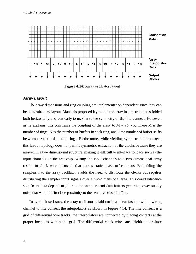
4.2 Clock Generation
46
Array Layout
The array dimensions and ring coupling are implementation dependant since they can
be constrained by layout. Maneatis proposed laying out the array in a matrix that is folded
both horizontally and vertically to maximize the symmetry of the interconnect. However,
as he explains, this constrains the coupling of the array to M = yN - k, where M is the
number of rings, N is the number of buffers in each ring, and k the number of buffer shifts
between the top and bottom rings. Furthermore, while yielding symmetric interconnect,
this layout topology does not permit symmetric extraction of the clocks because they are
arrayed in a two dimensional structure, making it difficult to interface to loads such as the
input channels on the test chip. Wiring the input channels to a two dimensional array
results in clock wire mismatch that causes static phase offset errors. Embedding the
samplers into the array oscillator avoids the need to distribute the clocks but requires
distributing the sampler input signals over a two-dimensional area. This could introduce
significant data dependent jitter as the samplers and data buffers generate power supply
noise that would be in close proximity to the sensitive clock buffers.
To avoid these issues, the array oscillator is laid out in a linear fashion with a wiring
channel to interconnect the interpolators as shown in Figure 4.14. The interconnect is a
grid of differential wire tracks; the interpolators are connected by placing contacts at the
proper locations within the grid. The differential clock wires are shielded to reduce
ConnectionMatrix
ArrayInterpolatorCells
Output
0 19 1 18 2 17 3 16 4 15 5 14 6 13 7 12 8 11 9 10
Figure 4.14: Array oscillator layout
Clocks

4.2 Clock Generation
47
coupling to other clock wires. While the grid provides equal capacitive loading, the length
of interconnect between interpolators is not uniform and introduces a built-in DNL of
about 8ps. Despite this limitation, the linear layout proves to be very useful when
designing the array as it permits freedom in setting the ring coupling factor while at the
same time allowing the matching of the physical placement of clock phases with the DLL.
This is important because the histogram counters are designed for a specific temporal
arrangement of the output data. Furthermore, the interconnect flexibility permits the
aforementioned trade-off between maximum oscillation frequency and adjustment range.
A drawback is that it does limit the operating frequency since every buffer must drive a
long wire.
4.2.4 Control Loop Design
The delay line and array oscillator create clocks evenly spaced within a period, but this
is insufficient by itself to achieve accurate timing, as the period must also be precisely
maintained by the control loop. Figure 4.15 and Figure 4.16 show the control loops for the
PLL and DLL respectively. The control loops are similar. Both have a phase detector to
measure the phase error between the two inputs and produce two outputs, UP and DOWN.
The width of the UP and DOWN output pulses depends on the arrival time of the input
edges. In response to the UP and DOWN pulses, the charge pump drives the control
I
IR
C
PhaseDetector
Fref
Fosc
LoopFilter
ChargePump
Vctrl
Figure 4.15: PLL control loop
Cextra
Implicit3rd Pole
UP
DOWN

4.2 Clock Generation
48
voltage with a current proportional to the pulses. The loop filter integrates the charge and
stabilizes the loop. The PLL phase detector is often slightly more complex than that of the
DLL because it contains additional logic to check for both frequency and phase lock to
prevent false frequency locking. In addition, the loop filter for the PLL is more complex
because it needs a zero to stabilize the additional pole introduced by the VCO. Cextra is
formed by the loading capacitance on Vctrl and introduces a 3rd pole in the transfer
function of the PLL control loop. This pole is leveraged later in this section to increase the
timing accuracy of the VCO.
An ideal phase detector generates no output when the input edges are exactly
coincident. When the inputs edges are not aligned, the output is UP or DOWN pulses with
widths proportional the phase shift between inputs. Real phase detectors however, cannot
transition from a zero to finite output for an arbitrarily small input phase difference. This
results in a deadband in the control loop when tracking small input phase errors. The
established practice to avoid this problem is to build a phase detector that always
generates output pulses. When the inputs edges are perfectly aligned, the UP and DOWN
output pulses are identical which, in theory, causes no change on the control voltage
because the net output of the charge pump is zero.
Unfortunately, real charge pumps have mismatch in the UP and DOWN paths which
causes synchronous ripple on the control voltage node. The charge pump used for both the
Figure 4.16: DLL control loop
I
I C
PhaseDetector
DLL Phase 0
LoopFilter
ChargePump
VctrlDLL Phase 20
UP
DOWN

4.2 Clock Generation
49
DLL and PLL is shown in Figure 4.17. When the UP and DOWN signals are asserted
simultaneously, the charge pump will initially remove charge from the control node
because M4 will be enabled before M8 due to the extra PMOS device, M6, that is in the
UP path. When M8 is turned on, the up and down currents will match and no additional
charge is added or removed from the control node. When the UP and DOWN pulses are
de-asserted, M4 will be turned off before M8 and charge will be injected onto the control
node.
The ripple on control voltage appears as synchronous noise to the buffers and
interpolators and, as described in Chapter 3, this results in static phase offsets. There are a
number of solutions to this problem; possibly the simplest for the PLL, and the one
implemented on the test chip, is to explicitly reduce the frequency of the 3rd pole as much
as possible while maintaining sufficient phase margin for stability. Typically this allows
the 3rd pole to be reduced to about an order of magnitude higher than the explicit pole set
by the loop filter.
A more complex, but effective design simulated for the test chip but not implemented,
is to split that charge pump into N copies, each 1/N the size of the original. The charge
pumps are clocked with the same UP/DOWN signals, but with a phase shift between each
charge pump. A block diagram for such a configuration is shown in Figure 4.18. The
UP DOWN
VBN
ICP
DOWNUPM12µ
M63µ
M9 M107µ
M53µ
M73µ
M83µ
M22µ
M32µ
M42µ
7µ
Figure 4.17: Control loop charge pump
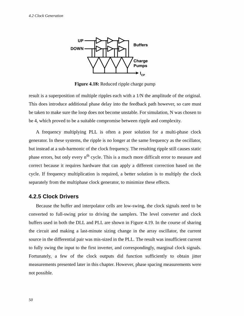
4.2 Clock Generation
50
result is a superposition of multiple ripples each with a 1/N the amplitude of the original.
This does introduce additional phase delay into the feedback path however, so care must
be taken to make sure the loop does not become unstable. For simulation, N was chosen to
be 4, which proved to be a suitable compromise between ripple and complexity.
A frequency multiplying PLL is often a poor solution for a multi-phase clock
generator. In these systems, the ripple is no longer at the same frequency as the oscillator,
but instead at a sub-harmonic of the clock frequency. The resulting ripple still causes static
phase errors, but only every nth cycle. This is a much more difficult error to measure and
correct because it requires hardware that can apply a different correction based on the
cycle. If frequency multiplication is required, a better solution is to multiply the clock
separately from the multiphase clock generator, to minimize these effects.
4.2.5 Clock Drivers
Because the buffer and interpolator cells are low-swing, the clock signals need to be
converted to full-swing prior to driving the samplers. The level converter and clock
buffers used in both the DLL and PLL are shown in Figure 4.19. In the course of sharing
the circuit and making a last-minute sizing change in the array oscillator, the current
source in the differential pair was mis-sized in the PLL. The result was insufficient current
to fully swing the input to the first inverter, and correspondingly, marginal clock signals.
Fortunately, a few of the clock outputs did function sufficiently to obtain jitter
measurements presented later in this chapter. However, phase spacing measurements were
not possible.
UP
DOWN
ChargePumps
Buffers
ICP
Figure 4.18: Reduced ripple charge pump
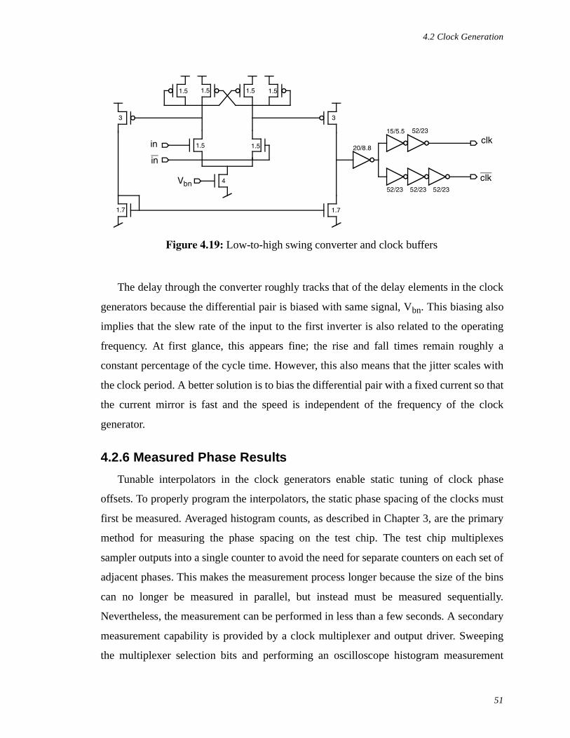
4.2 Clock Generation
51
The delay through the converter roughly tracks that of the delay elements in the clock
generators because the differential pair is biased with same signal, Vbn. This biasing also
implies that the slew rate of the input to the first inverter is also related to the operating
frequency. At first glance, this appears fine; the rise and fall times remain roughly a
constant percentage of the cycle time. However, this also means that the jitter scales with
the clock period. A better solution is to bias the differential pair with a fixed current so that
the current mirror is fast and the speed is independent of the frequency of the clock
generator.
4.2.6 Measured Phase Results
Tunable interpolators in the clock generators enable static tuning of clock phase
offsets. To properly program the interpolators, the static phase spacing of the clocks must
first be measured. Averaged histogram counts, as described in Chapter 3, are the primary
method for measuring the phase spacing on the test chip. The test chip multiplexes
sampler outputs into a single counter to avoid the need for separate counters on each set of
adjacent phases. This makes the measurement process longer because the size of the bins
can no longer be measured in parallel, but instead must be measured sequentially.
Nevertheless, the measurement can be performed in less than a few seconds. A secondary
measurement capability is provided by a clock multiplexer and output driver. Sweeping
the multiplexer selection bits and performing an oscilloscope histogram measurement
1.5 1.5 1.5 1.5
1.5 1.5
4
clk
clk
in
in
33
1.71.7
20/8.8
52/23 52/23 52/23
52/2315/5.5
Figure 4.19: Low-to-high swing converter and clock buffers
Vbn

4.2 Clock Generation
52
results in a plot similar to Figure 4.21. This technique is used to verify the measurements
made with the histogram counters but since the multiplexer has variable delay due to
mismatches in the input paths, the measurement technique is considered less accurate than
the histogram counters.
Figure 4.20 shows the histogram counter and multiplexers as implemented on the test
chip. Because the input clocks to the histogram counter always consist of an even and odd
clock, the multiplexers can be simplified by making one select between the even clocks
and the other select between the odd clocks. A 20-bit counter counts system cycles so that
each histogram runs for an equal period of time. The counters are implemented as linear-
feedback shift registers (LFSR) to simplify design and minimize the area required
compared to a regular binary counter. Decoding the LFSR count into a binary value is
performed off-line by a workstation.
The length of the histogram measurements can be configured to be up to 220 system
cycles. The total number of calibration edges depends on the frequency of the calibration
clock and it is desirable to have a high-frequency calibration source for higher
measurement resolution. The histogram measurements should be possible with a random
input frequency that is higher than the reference clock, but this was not verified in the lab.
Figure 4.20: Architecture for histogram measurements of phase offsets
Input Channel
10:1 10:1odd even
Counter
Counter
SystemClock
20
RandomInput
Signal
Clock Generator
20

4.2 Clock Generation
53
The laboratory measurements presented were performed with a 900MHz system clock and
calibration frequencies ranging between 200 and 400MHz. While theory may dictate that
the calibration source frequency needs to be carefully specified, laboratory results indicate
that a wide variation of frequencies will produce identical measurements and therefore a
random clock uncorrelated to the reference clock suffices for histogram measurements.
Figure 4.21 shows a histogram plot of a single DLL clock as the corresponding phase
interpolator is swept through all eight adjustment codes. Because sign-magnitude
encoding is used, two codes map to zero and hence the center peak is about twice as high
as the others. The spacing between peaks is about 7ps with a linearity of about 2ps. Based
on this data, the interpolators on the test chip are capable of statically placing an edge to
within about ±5ps. The high degree of linearity indicates that additional adjustment bits
are feasible and the static edge placement could be improved to better than ±2.5ps. As the
interpolator output phase data indicates, neither the nonlinear relationship between the
interpolation ratio, α, and output phase, nor mismatches in the adjustment transistors
significantly limit the output linearity of the interpolator.
The behavior of the counters was verified by moving a single clock phase and
measuring the size of the sampling bins on each side of the clock phase. The results of this
test are shown in Figure 4.22. The asynchronous input signal was at 351MHz and the
Figure 4.21: Histogram plot of interpolator output

4.2 Clock Generation
54
tester was clocked at 900MHz which resulted in each histogram hit representing about
1.4fs. The results of this experiment matched well with Figure 4.21, thus confirming the
accuracy of the measurement technique.
The phase spacing errors of the DLL, measured with the histogram counters, are
shown in Figure 4.23. Inexact current weighting in the interpolators due to device width
quantization causes the alternating phase error pattern because adjacent DLL clocks are
generated with the same interpolators but with inputs flipped. Therefore, one clock
appears early, while the next is late, and so forth. Folding of the DLL layout creates a
discontinuity at about midpoint in the plot. This error is due to imperfect wire matching in
the layout and is not necessarily a problem intrinsic to the design.
Also shown in Figure 4.23 are the phase spacings of the compensated DLL clocks.
The maximum expected error should be limited to half the resolution of the adjustment
step, ~4.5ps, indicated by the dashed horizontal lines. However, as evident in the plot,
some errors are larger than this value due to insufficient adjustment range of the
interpolator.
4.2.7 Phase Alignment Considerations
The inability of the DLL interpolators to fully correct for the static phase errors is due
to the limited adjustment range of the clock generator architecture. While data is
0
5000
10000
15000
20000
25000
30000
35000
40000
0 1 2 3 4 5 6 7
1-2 Spacing
2-3 Spacing
Interpolator Adjustment Code
His
togr
am C
ount
Figure 4.22: Correlation of histogram measurements to phase spacing
7ps
14ps
21ps
28ps
35ps
42ps
49ps

4.2 Clock Generation
55
unavailable for the PLL, experience with the DLL suggests that the PLL would also suffer
from insufficient adjustment. A solution is to build the clock generators with no
consideration for phase adjustment and instead, add a tunable delay vernier to each clock
phase. Not only does this yield simpler clock generator designs, but in the case of the array
oscillator, it will increase oscillation frequency.
A simple tunable differential delay element is shown in Figure 4.24. This element uses
a differential buffer and an adjustable interpolator to provide an adjustment range of up to
one buffer delay. A trade-off between range and resolution is possible by using both fixed
and digitally tunable current sources. The ratio of fixed current to adjustable current sets
the resolution and adjustment range. A reasonable adjustment range is plus or minus one
and a half sampling bins, which is approximately . A 4-bit adjustment range
would then yield steps of 1/24th of a FO-4 delay, or about 5ps on the test chip. This allows
edge placement to within ±2.5ps. Based on matching data from Figure 4.21, even 6-bit
resolution might be feasible. The issue becomes one of implementation cost, not of the
digital register bits required for storing the DAC coefficients or associated read/write
circuitry for the registers, but of the required interpolator DACs. This is due to the digital
circuitry roughly scaling linearly with the number of required adjustment bits, while the
-80
-60
-40
-20
0
20
40
60
80
100
Uncompensated
Compensated
20%=5.5ps
Figure 4.23: Compensated DLL phase spacing
+4.5ps
-4.5ps
Sampling Bins
%d
evia
tio
nfr
om
idea
l
FO-4 Delay3
----------------------------±
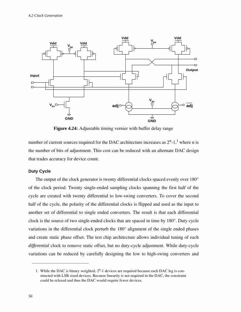
4.2 Clock Generation
56
number of current sources required for the DAC architecture increases as 2n-1,1 where n is
the number of bits of adjustment. This cost can be reduced with an alternate DAC design
that trades accuracy for device count.
Duty Cycle
The output of the clock generator is twenty differential clocks spaced evenly over 180°
of the clock period. Twenty single-ended sampling clocks spanning the first half of the
cycle are created with twenty differential to low-swing converters. To cover the second
half of the cycle, the polarity of the differential clocks is flipped and used as the input to
another set of differential to single ended converters. The result is that each differential
clock is the source of two single-ended clocks that are spaced in time by 180°. Duty cycle
variations in the differential clock perturb the 180° alignment of the single ended phases
and create static phase offset. The test chip architecture allows individual tuning of each
differential clock to remove static offset, but no duty-cycle adjustment. While duty-cycle
variations can be reduced by carefully designing the low to high-swing converters and
1. While the DAC is binary weighted, 2n-1 devices are required because each DAC leg is con-structed with LSB sized devices. Because linearity is not required in the DAC, the constraintcould be relaxed and thus the DAC would require fewer devices.
Vdd Vdd
GND
Vbn
VbpVdd Vdd
GND
Vbn
Vbp
adj
Input
Output
adj
Figure 4.24: Adjustable timing vernier with buffer delay range
4.2 Clock Generation
57
clock buffers, it is unreasonable to expect accuracy on the order of a few picoseconds.
Therefore duty-cycle variations can be a significant source of static phase error. Making
the duty-cycle individually adjustable or moving the timing adjustment after the
differential to singled-ended converters would solve this problem.
4.2.8 Phase Adjustment Summary
Digital phase tuning circuits are capable of placing clock edges with very high
precision. Edges on the experimental test chip could be placed to within ±5ps and data
indicates achieving ±2.5ps resolution should be feasible. This, coupled with the ability to
measure edge placement to an arbitrarily high degree of accuracy with histogram counters,
allows the clock phases to be aligned to better than twice what had been previously
reported for clock generators without phase tuning [6][23][37]. Because both the DLL and
PLL architectures are comprised of interpolators, it seems like to be the logical location
for the static phase adjustment capabilities. However, integrating the phase adjustment
into the clock generators involves many compromises and adding phase adjustment as
external verniers is worth investigating.
4.2.9 Timing Jitter
Having presented a technique to minimize static phase offsets with calibration, we
now look at techniques for minimizing the timing uncertainty due to dynamic jitter in the
clock generators. The magnitude of the jitter induced by a circuit depends on the delay
through the circuit and its sensitivity to noise.1 While, the clock generators use differential
delay elements with a low delay sensitivity they also use normal inverters in the clock
buffer chains so some jitter is inevitable. This section presents jitter measurements for the
clock generators and investigates the effectiveness of post-processing the sampler output
data to remove jitter from the measurements.
The effectiveness of the compensation depends on the correlation of jitter between
channels, so that a measurement from one channel can be used to correct data from
another channel. To maintain a high degree of correlation between sampling channels,
1. Reducing the delay of a circuit may not always be possible but in some cases, such as a clockbuffer chain, can be accomplished by optimizing the buffer fanout.
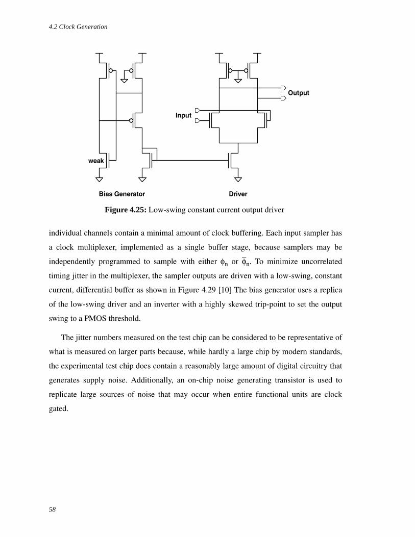
4.2 Clock Generation
58
individual channels contain a minimal amount of clock buffering. Each input sampler has
a clock multiplexer, implemented as a single buffer stage, because samplers may be
independently programmed to sample with either φn or φn. To minimize uncorrelated
timing jitter in the multiplexer, the sampler outputs are driven with a low-swing, constant
current, differential buffer as shown in Figure 4.29 [10] The bias generator uses a replica
of the low-swing driver and an inverter with a highly skewed trip-point to set the output
swing to a PMOS threshold.
The jitter numbers measured on the test chip can be considered to be representative of
what is measured on larger parts because, while hardly a large chip by modern standards,
the experimental test chip does contain a reasonably large amount of digital circuitry that
generates supply noise. Additionally, an on-chip noise generating transistor is used to
replicate large sources of noise that may occur when entire functional units are clock
gated.
DriverBias Generator
Input
Output
weak
Figure 4.25: Low-swing constant current output driver
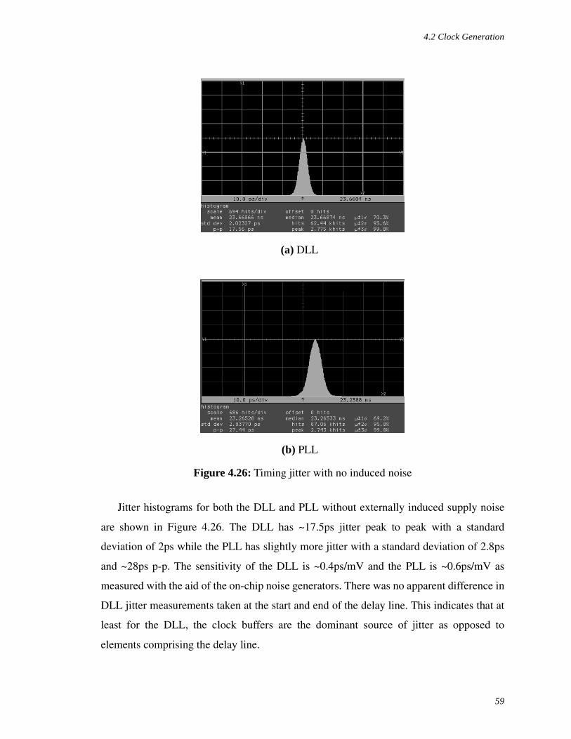
4.2 Clock Generation
59
Jitter histograms for both the DLL and PLL without externally induced supply noise
are shown in Figure 4.26. The DLL has ~17.5ps jitter peak to peak with a standard
deviation of 2ps while the PLL has slightly more jitter with a standard deviation of 2.8ps
and ~28ps p-p. The sensitivity of the DLL is ~0.4ps/mV and the PLL is ~0.6ps/mV as
measured with the aid of the on-chip noise generators. There was no apparent difference in
DLL jitter measurements taken at the start and end of the delay line. This indicates that at
least for the DLL, the clock buffers are the dominant source of jitter as opposed to
elements comprising the delay line.
(a) DLL
(b) PLL
Figure 4.26: Timing jitter with no induced noise
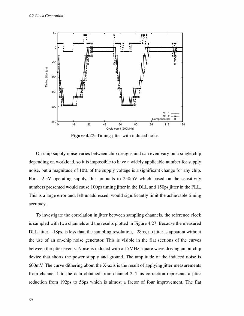
4.2 Clock Generation
60
On-chip supply noise varies between chip designs and can even vary on a single chip
depending on workload, so it is impossible to have a widely applicable number for supply
noise, but a magnitude of 10% of the supply voltage is a significant change for any chip.
For a 2.5V operating supply, this amounts to 250mV which based on the sensitivity
numbers presented would cause 100ps timing jitter in the DLL and 150ps jitter in the PLL.
This is a large error and, left unaddressed, would significantly limit the achievable timing
accuracy.
To investigate the correlation in jitter between sampling channels, the reference clock
is sampled with two channels and the results plotted in Figure 4.27. Because the measured
DLL jitter, ~18ps, is less than the sampling resolution, ~28ps, no jitter is apparent without
the use of an on-chip noise generator. This is visible in the flat sections of the curves
between the jitter events. Noise is induced with a 15MHz square wave driving an on-chip
device that shorts the power supply and ground. The amplitude of the induced noise is
600mV. The curve dithering about the X-axis is the result of applying jitter measurements
from channel 1 to the data obtained from channel 2. This correction represents a jitter
reduction from 192ps to 56ps which is almost a factor of four improvement. The flat
-250
-200
-150
-100
-50
0
50
0 16 32 48 64 80 96 112 128
Tim
ing
jitte
r (p
s)
Cycle count (900MHz)
Ch. 1Ch. 2
Compensated
Figure 4.27: Timing jitter with induced noise

4.2 Clock Generation
61
region at the bottom of the jitter curves is due to a delay change in uncompensated clock
buffers that are affected by the change in supply voltage when the noise generating
shorting transistor is enabled.
The correlation between phases is maximized by locating the drivers for the clock
buffers in close proximity and maintaining low-impedance power and ground busses
between the clock buffers. This ensures that power supply noise affects each of the clock
phases equally. High-frequency noise can cause jitter to be uncorrelated from phase to
phase. To reduce the frequency content of the supply noise and hence the resulting jitter,
significant amounts of bypass capacitance is placed between the power rails of the clock
buffers.
Because of physical proximity, it would be expected that channels 1 and 2 would
display a higher correlation than channels 1 and 7, however lab measurements were
unable to measure any difference in correlation. Thus, if a difference exists, it is less than
the resolution of the sampling system. Furthermore, changing the phase alignment of the
two input signals using off-chip, passive delay elements did not produce a measurable
change in the correlation between channels.
While this data indicates the feasibility of canceling on-chip supply noise, it is
interesting to consider if it is also possible to remove any component of the jitter that
exists without induced noise. This is a challenging measurement because the jitter of the
DLL is less than the sampling resolution of the system. To increase the resolution of the
measurement, an alternate approach was used by taking advantage of the tester’s ability to
bypass the SR-latch following the sampler and instead capture the logical NOR of the
sampler outputs. This feature was intended to be a completion detect so the phase
alignment of the sampler and the digital system clock could be determined. However, it
proved useful for this measurement because it allows the measurement of the metastability
window over which the sampler does not resolve because of insufficient gain. The width
of this window can be controlled by setting the input signal voltage. The larger the input
swing, the narrower the metastability window.
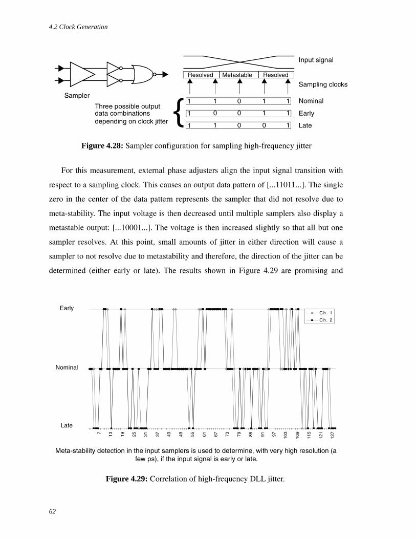
4.2 Clock Generation
62
For this measurement, external phase adjusters align the input signal transition with
respect to a sampling clock. This causes an output data pattern of [...11011...]. The single
zero in the center of the data pattern represents the sampler that did not resolve due to
meta-stability. The input voltage is then decreased until multiple samplers also display a
metastable output: [...10001...]. The voltage is then increased slightly so that all but one
sampler resolves. At this point, small amounts of jitter in either direction will cause a
sampler to not resolve due to metastability and therefore, the direction of the jitter can be
determined (either early or late). The results shown in Figure 4.29 are promising and
Input signal
Sampling clocks
1 1 0 1 1
1 0 0 1 1
1 1 0 0 1
NominalSampler
Resolved ResolvedMetastable
Early
LateThree possible output
data combinationsdepending on clock jitter
Figure 4.28: Sampler configuration for sampling high-frequency jitter
0
1
2
1 7 13 19 25 31 37 43 49 55 61 67 73 79 85 91 97 103
109
115
121
127
C h. 1
C h. 2
Early
Nominal
Late
Figure 4.29: Correlation of high-frequency DLL jitter.
Meta-stability detection in the input samplers is used to determine, with very high resolution (a few ps), if the input signal is early or late.

4.3 Samplers
63
indicate that the jitter is correlated at least in its direction. Further work with improved
measurement accuracy is needed to completely characterize this behavior.
Timing jitter on large digital parts is predominantly caused by digital switching noise
on power and ground and, even with careful circuit design and layout, it can significantly
limit the achievable timing resolution. To compensate for this limitation, the experimental
test chip measures cycle-to-cycle jitter and removes it from the sampled data by post-
processing. Measured results indicate that this correction is feasible in practice and can
improve measurement accuracy significantly. This is useful for achieving high timing
accuracy as jitter is a significant problem on large VLSI parts.
4.3 SamplersHaving looked at clock generation issues, this section now considers the sampler
circuit that interfaces with the clocks. The important sampler characteristics are aperture,
input capacitance and the input-referred offset voltage. The sampler used on the test chip,
shown in Figure 4.30, consists of a pair of cross coupled inverters composed of transistors
M3 through M6 with variable-strength pull-down paths controlled by M1 and M2 [27].
When clk is high, M7 through M9 reset and equalize the upper nodes of the sampler,
When clk rises, M10 is enabled and a differential current is injected into the upper nodes
in in
out out
clk
clk
M1 M2
M3 M4
M5 M7 M8 M6
M9
M10
3.2µ 3.2µ
3.2µ 3.2µ
3.2µ
3.2µ3.2µ3.2µ 3.2µ
6.4µAll devices have L=0.24m
Figure 4.30: Input sampler

4.3 Samplers
64
of the sampler where it is amplified and generates the output. The design is small, simple,
fast, and requires only a single clock phase.
To minimize input capacitance, M1 and M2 must be small. However, small devices
exhibit poor matching characteristics that cause timing errors. It is not inconceivable for a
30mV offset to cause a 30ps timing error for a 1Gb/sec input signal.1 While all the
differential devices contribute to the offset, the devices that contribute most are M1 and
M2 as shown in Table 1.
Given that M1 and M2 are the dominant source of mismatch, the offset voltage can be
approximated as:
Here σVT is the standard deviation of the device threshold voltage and can be
approximated as , where α is a technology dependant constant [9][30]. For the
process used to implement the test chip α is about 6mV. For M1 and M2, which on the test
chip are 0.25µm x 3.2µm, σVT is 9.45mV. The simulated Monte Carlo data which agrees
well with the manual offset calculation is shown in Figure 4.31.
1. Assuming the rise and fall times of 1/3 of the period and the signal swing is 333mV; numberswhich are quite typical and representative of high-speed I/O.
Transistors Sensitivity
M1 and M2 1 mV/mV
M3 and M4 0.108 mV/mV
M5 and M6 0.091 mv/mV
Table 1: Input offset sensitivity to device Vt variations
Vofs 3σVT 2.⋅=
α um⋅W L⋅
-----------------
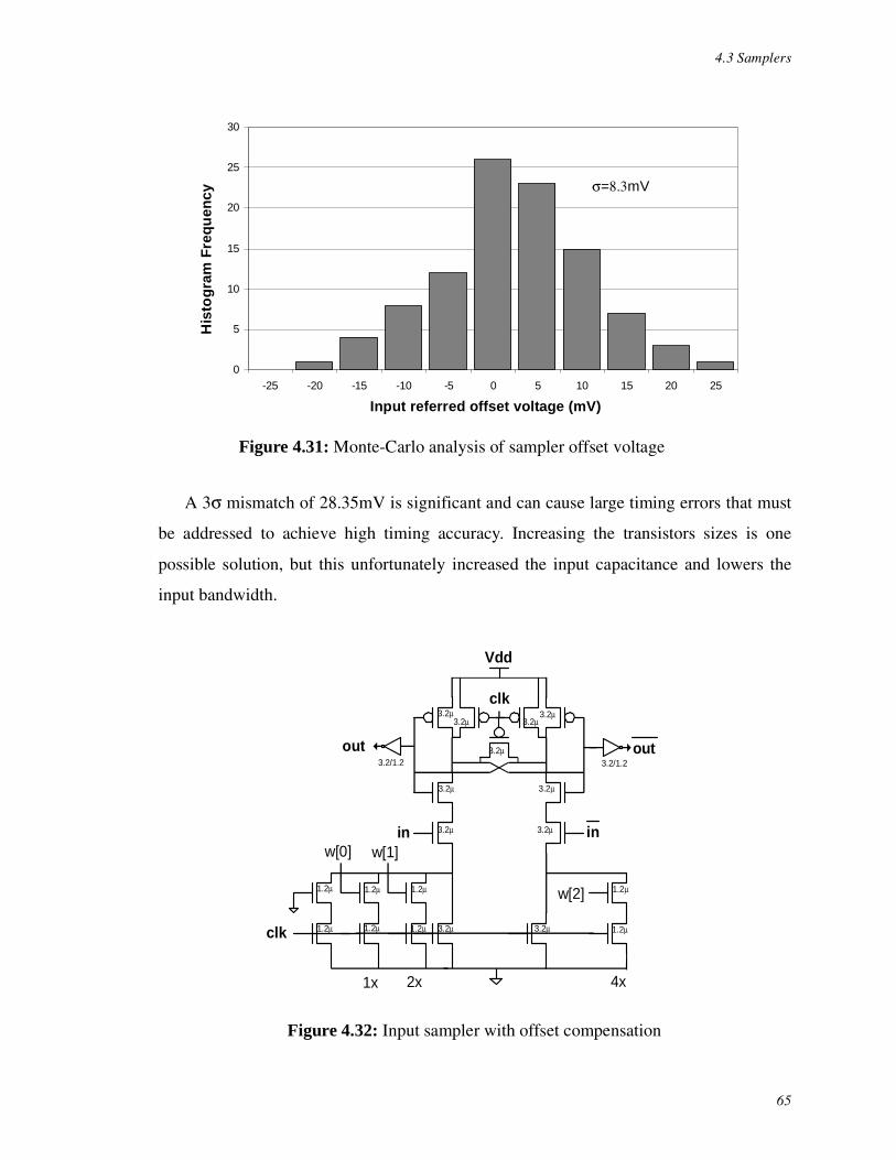
4.3 Samplers
65
A 3σ mismatch of 28.35mV is significant and can cause large timing errors that must
be addressed to achieve high timing accuracy. Increasing the transistors sizes is one
possible solution, but this unfortunately increased the input capacitance and lowers the
input bandwidth.
0
5
10
15
20
25
30
-25 -20 -15 -10 -5 0 5 10 15 20 25
His
tog
ram
Fre
qu
ency
Input referred offset voltage (mV)
σ=8.3mV
Figure 4.31: Monte-Carlo analysis of sampler offset voltage
clk
in in
out out
w[0] w[1]
w[2]
Vdd
clk
1x 2x 4x
3.2µ3.2µ 3.2µ
3.2µ
3.2µ
3.2µ 3.2µ
3.2µ 3.2µ
3.2µ3.2µ1.2µ
1.2µ
1.2µ
1.2µ
1.2µ
1.2µ1.2µ
1.2µ
3.2/1.23.2/1.2
Figure 4.32: Input sampler with offset compensation
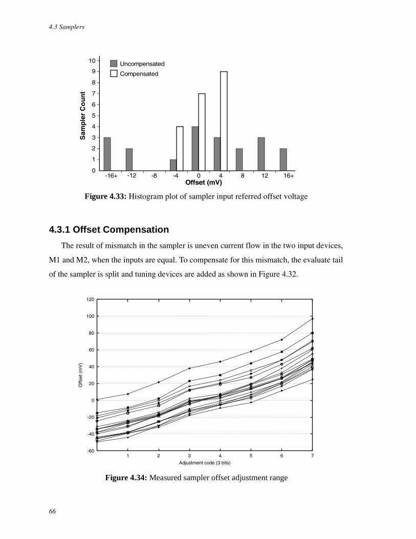
4.3 Samplers
66
4.3.1 Offset Compensation
The result of mismatch in the sampler is uneven current flow in the two input devices,
M1 and M2, when the inputs are equal. To compensate for this mismatch, the evaluate tail
of the sampler is split and tuning devices are added as shown in Figure 4.32.
Figure 4.33: Histogram plot of sampler input referred offset voltage
0
1
2
3
4
5
6
7
8
9
10
-16+ -12 -4 0 4 8 12 16+-8
Uncompensated
Compensated
Offset (mV)
Sam
ple
r C
ou
nt
-60
-40
-20
0
20
40
60
80
100
120
1 2 3 4 5 6 7
Offs
et (
mV
)
Adjustment code (3 bits)
Figure 4.34: Measured sampler offset adjustment range

4.3 Samplers
67
To calibrate these devices, the inputs are set to the expected common mode level and
the trimming devices are swept until the output of the sampler toggles. The measured
offsets of 20 samplers on the experimental test chip are shown in Figure 4.33, both before
and after calibration. The adjustment range of the tuning devices with a 1V common mode
input is shown in Figure 4.34. The tuning range is reasonably linear and demonstrates the
ability to correct sampler offset to within ±5mV.
The key challenge with static offset compensation in a sampler is maintaining the
corrected input offset over operating condition variations. As shown in Figure 4.35, the
compensation tracks well over temperature and even a 75°C temperature swing will only
result in an offset change of a few millivolts. The gain of the sampler input transistors is
0 1 2 3 4 5 6 7-40
-30
-20
-10
0
10
20
30
Adjustment Code
Inpu
t ref
erre
d of
fset
vol
tage
25C 50C 75C 100C
Figure 4.35: Sampler offset compensation stability versus temperature
Inpu
t ref
erre
d of
fset
vol
tage
(m
V)
0 1 2 3 4 5 6 7-30
-20
-10
0
10
20
30
Adjustment Code
Inpu
t ref
erre
d of
fset
vol
tage
1.00V1.02V1.04V1.06V1.08V1.10V
Figure 4.36: Sampler offset compensation stability versus input common-mode
Inpu
t ref
erre
d of
fset
vol
tage
(m
V)

4.3 Samplers
68
dependent on the gate overdrive. Therefore, changes in the common-mode level of the
input signal will alter the offset compensation and translate common-mode noise into
differential noise. The sensitivity of the sampler offset to common-mode changes is
plotted in Figure 4.36. Transistor Vt variations are not the only sources of error, as β
mismatches also contribute. In Figure 4.37 the width of one of the input devices is swept
and the ∆width that nullifies the offset due to the calibration circuit is plotted for each
adjustment code. The resulting plot indicates that β mismatch compensation is quite stable
in the presence of common-mode noise.
0 1 2 3 4 5 6 7-12
-10
-8
-6
-4
-2
0
2
4
6
Adjustment Code
Eq
uiva
len
t Dev
ice
Wid
th V
aria
tion
(%)
1.00V1.02V1.04V1.06V1.08V1.10V
Figure 4.37: Sampler beta compensation stability versus common-mode
0 20 40 60 80 100 120-0.2
0
0.2
0.4
0.6
0.8
1
1.2
Time (ps)
Nor
mal
ized
Vol
tage
(V
)
Figure 4.38: Sampler step and impulse responses
Sampling Impulse
Step Response

4.4 Floorplan
69
4.3.2 Aperture
With a common mode voltage of 1.8V, the simulated aperture of the input latch used in
the test chip is 15ps. It is difficult to drive the sampler with an ideal impulse function to
measure the impulse response, so instead, a unit step response was measured and is plotted
in Figure 4.38. This was then differentiated to yield the sampling impulse shown in the
same plot. An FFT of the sampling impulse is shown in Figure 4.39 and indicates the -3dB
frequency of the low-pass filter due to the sampling aperture is about 6.9GHz. This is
sufficiently large as to not present a practical limit to the achievable timing accuracy of the
system.
4.4 FloorplanA micrograph of the test chip is shown in Figure 4.40. The PLL and DLL clock
generators are pitch matched with the sampling channel wiring to minimize wiring cost.
The analog input signals flow into the sampling channels from the left hand side and
digital data flows out the right into synchronization blocks that down convert the data
from 900MHz to 450MHz. The data processing of the chip is mirrored about the
109
1010
1011
-15
-14
-13
-12
-11
-10
-9
-8
-7
-6
-5
-4
-3
-2
-1
0
1
Frequency (Hz)
dBc
Figure 4.39: Frequency spectrum of sampling impulse
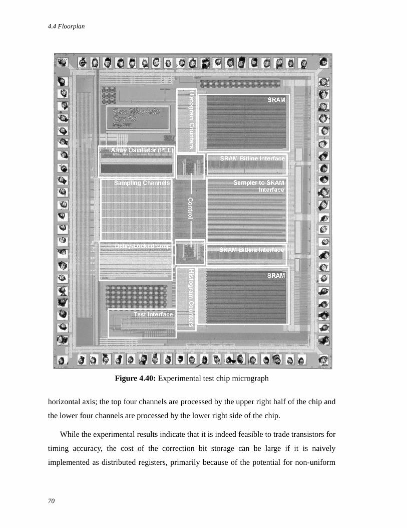
4.4 Floorplan
70
horizontal axis; the top four channels are processed by the upper right half of the chip and
the lower four channels are processed by the lower right side of the chip.
While the experimental results indicate that it is indeed feasible to trade transistors for
timing accuracy, the cost of the correction bit storage can be large if it is naively
implemented as distributed registers, primarily because of the potential for non-uniform
Figure 4.40: Experimental test chip micrograph

4.5 Summary
71
wiring. To minimize the cost of the correction bits, the storage is implemented as an
SRAM that overlays the clock generators and sampling cells. The SRAM cells are directly
wired to the tuning transistors and accessed in a standard manner with bit and word lines.
The word line decoders are to the left of the sampling channels and the bit lines reside at
the top of the PLL. All correction, configuration, and status bits on the part are memory
mapped and accessed by the host computer through an interface that mimics that of a
discrete SRAM. The design of both the correction bits and the digital interface yields a
compact and regular layout that minimizes the cost of the digital compensation circuitry.
The calibration algorithms are implemented in software on a workstation for
flexibility. A 20-bit data port interfaced to the workstation is used for compete read/write
access to all configuration bits and control registers.
4.5 SummaryStatic phase errors, timing jitter, sampler input offset voltage, and input capacitance
are the primary challenges of implementing a CMOS oversampled receiver with high
timing accuracy. Because of aggressive CMOS scaling, the most abundant resource
available to address these problems is transistors. Static phase compensation is probably
the most robust of the implemented techniques and results indicate that placing the
nominal position of a clock edge to within a couple picoseconds is feasible. The phase
tuning algorithm is driven by histogram counters that precisely measure phase offsets
without introducing additional timing errors. In the test chip, the primary limitation to
uniform phase spacing appears to be the complexity and size of the current-mode digital-
to-analog converters used in the interpolators.
Jitter compensation functions well on the test chip but is in part limited by the
sampling resolution. Higher resolution would also permit more accurate correlation
measurement between channels. The correlation demonstrated on the test chip is quite
high, but only measurable with significant and somewhat unrealistic supply noise.
Nevertheless, the test results indicate that this is a promising technique and could even
apply to fields other than testing, such as communication links.

4.5 Summary
72
Digital sampler offset compensation demonstrates the ability to reduce offset voltages
to within ± 5mV. Effective offset compensation permits small sampler input devices and
hence a higher input bandwidth. The technique used for offset compensation on the test
chip works well for signals with a fixed common-mode voltage such as that generated by
laboratory pulse generator, but is less effective for signals that have large common-mode
noise. Offset compensation that better tracks the device mismatch mechanisms appears to
be an area worthy of further research.

5.1 A Minimal Sampling System
73
Chapter 5
Integrated Testing
“If you knew what you were doing, you'd probably be bored”
- Fresco's Law
As the number of devices on die continues to scale, it might become cheaper to integrate a
small tester on each die, rather than do all the testing with an external device. This chapter
investigates the new issues that need to be addressed in order to integrate testers onto
production parts. Section 5.1 first examines what minimal amount of hardware is required
on-chip to enable the acquisition of edge transition information. Techniques to minimize
the impact of the receiver on the part without sacrificing timing accuracy are also
presented. Compression and decimation are covered in Section 5.2 as methods for
reducing the significant output data that even a minimal oversampling system can
generate. A motivation for integrating part of the tester on-chip is to make testing easier,
but before it can be used, the on-chip tester itself must be tested which is the subject of
Section 5.3.
5.1 A Minimal Sampling SystemOn a large chip, there are most likely a large number of signals whose timing is of
interest. Unfortunately, Murphy’s Law all but guarantees that the signals are as physically
dispersed as possible. This means that either multiple sampling systems are required on a
die, or that the signals must be routed to a single, shared sampling system. While the cost
of a sampling system is not high relative to the transistor budgets of large CMOS ICs,
integrating multiple sampling systems on a single die is not a favorable option for two
reasons. First, multiple sampling systems imply more transistors, which require area that
is not only costly in terms of dollars but also increases the distance between blocks and
thus the critical paths within the chip. Second, despite the techniques presented in Chapter
4 for contending with on-chip supply noise, it is still desirable to isolate the sampling
system with wide substrate guard rings and substantial amounts of bypass capacitance.
5.1 A Minimal Sampling System
74
Dropping a sampling system into the middle of a power-hungry and noisy digital block is
probably not the most effective way of obtaining high timing accuracy. Therefore, it is
advantageous to build a single sampling system that is relatively isolated on an edge of the
die. This both minimizes its impact on existing circuitry and reduces timing errors due to
noise coupled via the supply and substrate.
A single measurement circuit will have to contend with the uncertain delay in the wire
and possible repeaters used to connect signals being instrumented to the sampling system.
Even relatively short wires, as compared to a die size of 1cm2, can produce a significant
timing error because the propagation velocity of light in SiO2 is about 7ps/mm. A 2mm
wire would introduce an error comparable to the timing resolution of the sampling system
presented in the previous chapter. Longer wires are worse and the minimum delay across a
1cm die, including repeaters, is about 400ps in a 0.25µm process. Obviously, high-
precision timing measurements require a method to remove wire delay.
Differential timing measurements are a solution to this problem. Rather than
measuring the timing of an edge transition relative to a absolute timing source, the edge is
measured relative to the local clock that interfaces with that signal. This usually is a more
useful measurement, because what is often of interest is setup and hold times of a circuit
rather than the exact timing. If the clock and data both jitter together, then the setup and
hold times are maintained, but this is not apparent if a local clock is not also measured.
Therefore, by routing the local clock and signal of interest together across the chip, the
delay of the interconnect, to first order, can be removed from the measurement.
Differential measurements require an additional sampling channel and the resulting
sampling system that represents the minimal hardware required is shown in Figure 5.1.
Using the test chip presented in the previous chapter as a benchmark, such a sampling
system can be built with about twenty thousand transistors and occupy an area of about
0.2mm2 in a 0.25µm process technology.
While differential measurements allow accurate relative timing measurements for
signals located in close proximity, there is still the issue of measuring the timing between
signals located on physically disparate parts of a chip. An example would be to measure
global clock skew. It is unreasonable to assume that it is possible to match the delays of all
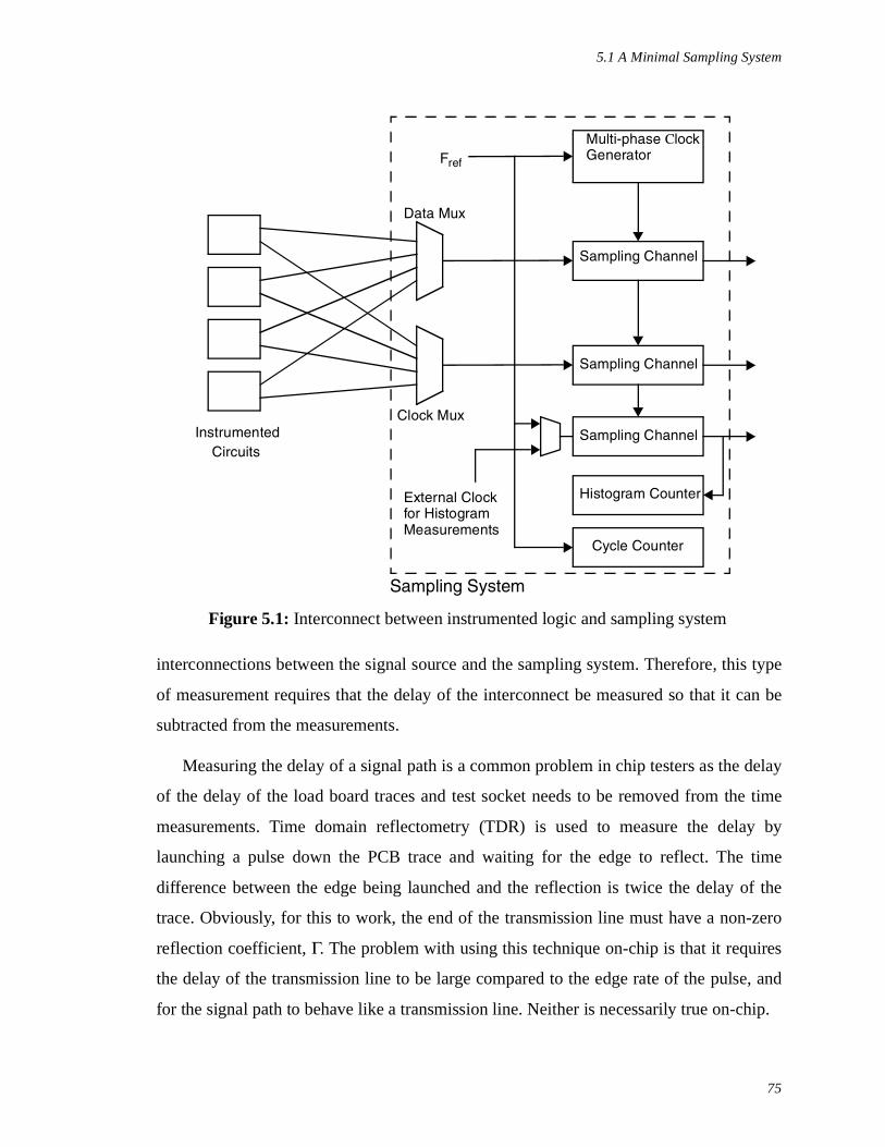
5.1 A Minimal Sampling System
75
interconnections between the signal source and the sampling system. Therefore, this type
of measurement requires that the delay of the interconnect be measured so that it can be
subtracted from the measurements.
Measuring the delay of a signal path is a common problem in chip testers as the delay
of the delay of the load board traces and test socket needs to be removed from the time
measurements. Time domain reflectometry (TDR) is used to measure the delay by
launching a pulse down the PCB trace and waiting for the edge to reflect. The time
difference between the edge being launched and the reflection is twice the delay of the
trace. Obviously, for this to work, the end of the transmission line must have a non-zero
reflection coefficient, Γ. The problem with using this technique on-chip is that it requires
the delay of the transmission line to be large compared to the edge rate of the pulse, and
for the signal path to behave like a transmission line. Neither is necessarily true on-chip.
InstrumentedCircuits
Sampling Channel
Sampling Channel
Data Mux
Clock MuxSampling Channel
Multi-phase ClockGeneratorFref
External Clockfor HistogramMeasurements
Histogram Counter
Cycle Counter
Sampling System
Figure 5.1: Interconnect between instrumented logic and sampling system
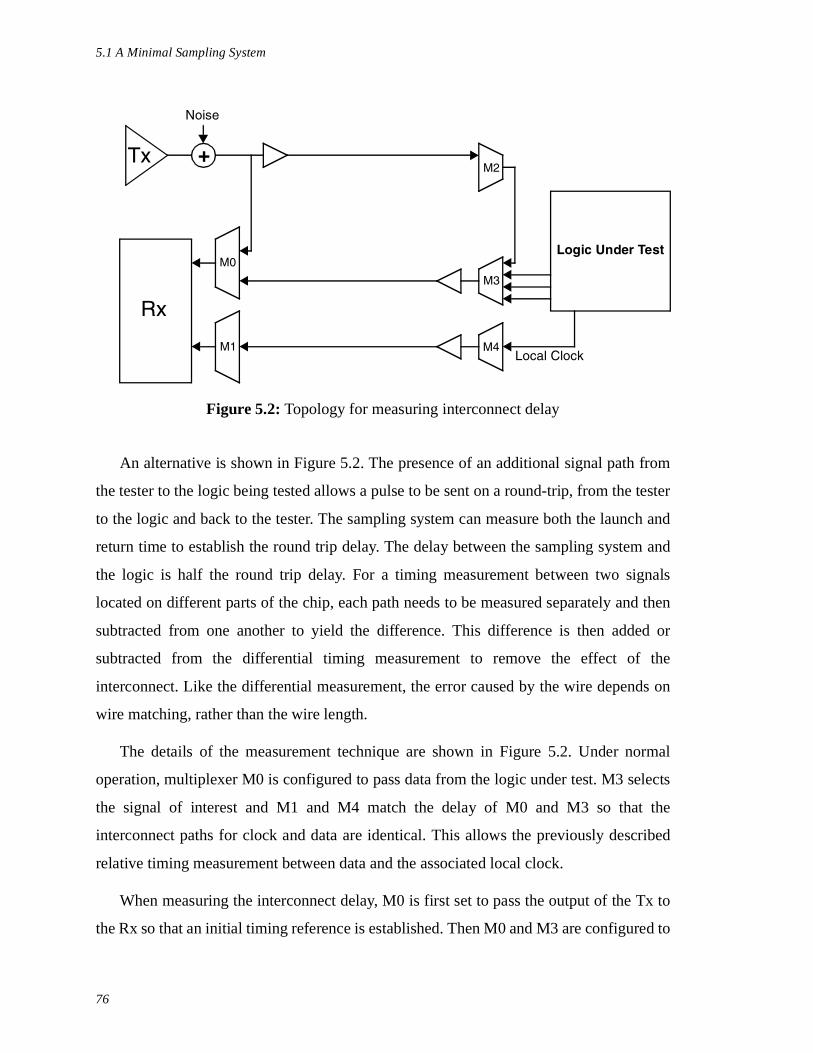
5.1 A Minimal Sampling System
76
An alternative is shown in Figure 5.2. The presence of an additional signal path from
the tester to the logic being tested allows a pulse to be sent on a round-trip, from the tester
to the logic and back to the tester. The sampling system can measure both the launch and
return time to establish the round trip delay. The delay between the sampling system and
the logic is half the round trip delay. For a timing measurement between two signals
located on different parts of the chip, each path needs to be measured separately and then
subtracted from one another to yield the difference. This difference is then added or
subtracted from the differential timing measurement to remove the effect of the
interconnect. Like the differential measurement, the error caused by the wire depends on
wire matching, rather than the wire length.
The details of the measurement technique are shown in Figure 5.2. Under normal
operation, multiplexer M0 is configured to pass data from the logic under test. M3 selects
the signal of interest and M1 and M4 match the delay of M0 and M3 so that the
interconnect paths for clock and data are identical. This allows the previously described
relative timing measurement between data and the associated local clock.
When measuring the interconnect delay, M0 is first set to pass the output of the Tx to
the Rx so that an initial timing reference is established. Then M0 and M3 are configured to
Rx
+Tx
Logic Under Test
Local Clock
Noise
M2
M0
M1
M3
M4
Figure 5.2: Topology for measuring interconnect delay

5.1 A Minimal Sampling System
77
pass the output of the Tx back to the Rx along the same path the data normally transits.
The difference between these two measurements is the total round trip delay.
The finite resolution of the sampling system will result in a quantization error equal to
half the sampling resolution, τ. Because two measurements are required to establish the
delay of the interconnect, one to measure the time the edge is sent and another to measure
when the edge is received, the resulting peak error will be twice as large. Furthermore,
consider the use of this delay measurement: it is subtracted from another path delay to
yield a net difference. This subtraction will yet again double the error, resulting in a peak
error of 2τ, which may be too large for some systems.
Interestingly, introducing a small amount of noise can reduce this error. The noise
source shown in the upper left of Figure 5.2 decreases the quantization error of the system.
If the Tx transmits a pulse with a small amount of jitter relative to the sampling resolution
of the receiver, then the accuracy of the timing measurement will be limited by the
sampling resolution as shown in Figure 5.3(a). However, introducing noise into the Tx so
that a histogram of the sampled output spans multiple sampling bins increases the
resolution of the measurement. By building a histogram of the captured edge, as shown in
Figure 5.3(b), the center point of the histogram, which is the nominal location of the Rx
clock edge, can be established to an arbitrarily high degree of precision by calculating the
timeTransmitter Histogram Received Signal Histogram
Received Signal Histogram
Quantized Histogramtime
timetime
time
time
Transmitter Histogram (w/ jitter)
(a) No Induced Jitter on Transmitter Output
(b) Induced Jitter on Transmitter Output
Quantized Histogram
Figure 5.3: Increasing static delay measurement with induced jitter

5.1 A Minimal Sampling System
78
moment of the resulting data. The induced jitter need not have any specific histogram
shape, but it is required that the histogram be symmetric unless more complex post-
processing is performed.
While the controlled introduction of jitter into the transmitter is beneficial in some
cases, jitter in the clock and data paths is not. For relative measurements, i.e. those that
compare transitions to the local digital clock, the jitter is canceled out provided the two
signal paths are constructed so that the buffers and multiplexers are physically close so
they can share the same supplies and have the same substrate noise. However, for absolute
measurements, i.e. those that attempt to subtract out the delay of the signal path
connecting the logic under test and the tester, jitter in the signal path will reduce the
accuracy of the measurement unless only an averaged value is desired.
In addition to jitter, static timing errors due to device mismatch can limit the timing
accuracy of the measurement. But, if the signal path between the instrumented logic and
the tester is full-swing static CMOS, it can match very well (to within a few picoseconds is
reasonable). The 1σ mismatch for a 4-inverter chain with 800µm of total metal load, as
8µ/.28µ
3.5µ/.28µ
8µ/.28µ
3.5µ/.28µ
8µ/.28µ
3.5µ/.28µ
8µ/.28µ
3.5µ/.28µ
SS, 2.25V, 100ºC, σ = 1.53ps TT, 2.5V, 50ºC, σ = 1.04ps
200µ/.6µ
26Ω, 34fF
200µ/.6µ
26Ω, 34fF
200µ/.6µ
26Ω, 34fF
200µ/.6µ
26Ω, 34fF
Figure 5.4: Matching for 800µm of interconnect
µ=2.54463nsσ=1.5331pN=100
µ=2.38831nsσ=1.0408pN=100
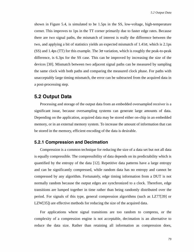
5.2 Output Data
79
shown in Figure 5.4, is simulated to be 1.5ps in the SS, low-voltage, high-temperature
corner. This improves to 1ps in the TT corner primarily due to faster edge rates. Because
there are two signal paths, the mismatch of interest is really the difference between the
two, and applying a bit of statistics yields an expected mismatch of 1.41σ, which is 2.1ps
(SS) and 1.4ps (TT) for this example. The 3σ variation, which is roughly the peak-to-peak
difference, is 6.3ps for the SS case. This can be improved by increasing the size of the
devices [30]. Mismatch between two adjacent signal paths can be measured by sampling
the same clock with both paths and comparing the measured clock phase. For paths with
unacceptably large timing mismatch, the error can be subtracted from the acquired data in
a post-processing step.
5.2 Output DataProcessing and storage of the output data from an embedded oversampled receiver is a
significant issue, because oversampling systems can generate large amounts of data.
Depending on the application, acquired data may be stored either on-chip in an embedded
memory, or in an external memory system. To increase the amount of information that can
be stored in the memory, efficient encoding of the data is desirable.
5.2.1 Compression and Decimation
Compression is a common technique for reducing the size of a data set but not all data
is equally compressible. The compressibility of data depends on its predictability which is
quantified by the entropy of the data [12]. Repetitive data patterns have a large entropy
and can be significantly compressed, while random data has no entropy and cannot be
compressed by any algorithm. Fortunately, edge timing information from a DUT is not
normally random because the output edges are synchronized to a clock. Therefore, edge
transitions are lumped together in time rather than being randomly distributed over the
period. For signals of this type, general compression algorithms (such as LZ77[39] or
LZW[35]) are effective methods for reducing the size of the acquired data.
For applications where signal transitions are too random to compress, or the
complexity of a compression engine is not acceptable, decimation is an alternative to
reduce the data size. Rather than retaining all information as compression does,
5.2 Output Data
80
decimation selectively discards sampler output data to reduce the bandwidth and memory
requirements. The selection of the data that is retained as opposed to discarded determines
the recorded signal characteristics and is therefore highly dependant on application.
For setup and hold checks, only the timing of the edges that proceed and follow the
clock is required. This requires storing a maximum of two transition per cycle regardless
of the number of transitions that actually occur. Superfluous edges are discarded. Data
acquisition can be further improved by encoding the edge information with varying
precision as shown in Figure 5.5a. The timing of data edges that fall close to the clock
edge can be encoded with more information than those that fall father away. For instance,
if the data input to a flip-flop arrives 1ns before the clock and the setup time is 200ps, then
the signal has a large margin and it matters little if the arrival time is 1.1ns or 900ps before
the clock edge. However, if the signal arrives only 250ps before the clock, a timing error
of 100ps in the tester is very important. Logarithmically encoding edge transitions, as
shown in Figure 5.5b, can be easily achieved in an oversampled system by discarding
predefined samples. More precise logarithmic encoding is possible by skewing the phase
of the sampling clocks in a logarithmic fashion to increase the timing accuracy of some
sampling bins. A drawback to skewing the clocks is that unless the sampling system has
per channel clock tuning capabilities, clock skew on a per-channel basis is not possible.
Selective edge capture is useful for setup and hold checks, but less so for capturing
glitches and other high-speed phenomena. For this type of application, capturing all
time
V(t)
Late signals need Less timing accuracy required
V(t)
more accuracy
Expected Transition Band Logarithmically Encoded Over-Sampling
time
Figure 5.5: Logarithmically encoded edge information

5.2 Output Data
81
transitions over a fixed window within the period rather than looking for specific
transitions results in more useful information. As shown in Figure 5.6, the sampling
windows can be predefined and data outside the window discarded. The reduction in data
size is set by the ratio of the bits stored versus those discarded. This was the approach used
in the test chip, presented in Chapter 4, to reduce the data bandwidth by a factor of two.
With only a small hardware cost (as shown by the test chip in the previous chapter), the
sampling windows can be made individually programmable to allow sampling of signals
that are not phase aligned.
For production test, complete edge information may not be required, and so the
storage of output data can be reduced. What can be useful however, is to know how close
an output signal is to being outside specification. A production tester can check for a valid
logic level at a predefined time with a cycle in addition to performing edge detection and
time
V(t)
SaveDiscard Discard
Figure 5.6: Window based decimation of sampler data
Raw DataEdge Detect Statistical Encoder
time
V(t)
Storage
Figure 5.7: Edge detection and compression

5.2 Output Data
82
record the cycles with the smallest margins. This can be useful when debugging data-
dependent timing errors and characterizing a part during production test. A simple
application of this concept is shown in Figure 5.7. Edge detection logic locates the last
valid transition and stores it in a compressed form using a statistical encoder such as a
Huffman coder [16]. A Huffman coder is a general compression engine that analyzes a
stream of numbers and codes the numbers that appear more frequently with fewer bits
while using more bits for less frequent numbers.
5.2.2 Jitter Compensation
If all the sampled data is dumped to a memory for post-processing, then on-the-fly
jitter correction is not required. However, if the data is processed and decimated in some
form, then it is advantageous to preform the jitter correction prior to decimation to ensure
that the correct information is retained. For instance, logarithmic encoding stores the data
with varying resolution depending on how far the edge transition is from the expected
transition point, but that difference is not known until after the jitter compensation has
been applied.
Input Channel
Input Channel
Barrel Shifter
Ref. Clk
Data
Edge Detect
Low-Pass Filter
Jitter Compensated Data
Figure 5.8: Real-time jitter compensation
+
Σ -
ClockGenerator

5.3 Testing the Tester
83
Figure 5.8 shows a block diagram an for on-the-fly jitter compensation design. A
dedicated input channel is used to sample the reference clock and the reference clock edge
is detected and averaged by a low-pass averaging filter to calculate the nominal clock
phase. The nominal clock phase is subtracted from the instantaneous phase to yield the
jitter, which programs a barrel shifter to adjust the sampled data from the other sampling
channels. The shifter need not be a complete barrel shifter as the shift operation is
constrained to the maximum range of the jitter.
5.2.3 Edge Filtering
A high sample rate and slow input edge rate may result in non-monotonic transitions,
such as 00010111, in the binary output stream due to sampling noise and sampler offsets.
Low-pass filtering is required to extract the edge transitions and is quite simple when
performed as a post-processing step. But if it must be done at speed, then it becomes
expensive in terms of both area and power. A 3-bit majority vote is a good trade-off
between performance and implementation cost. It converts the previous example of
00010111 into 00001111, to enable simple XOR edge detection. The amount of filtering
required depends on the sampling resolution and input slew rate. For sampling of on-chip
signals, simulation indicates edge filtering is not required unless the sampling resolution is
finer than 0.25 of a FO-4 delay.
5.3 Testing the TesterEmbedding a tester on a VLSI part enables more enlightening and less expensive
testing. However, a drawback is that the tester itself now needs to be tested. Making the
inputs to the sampling channels externally accessible permits sampling of known data
patterns and verification of the sampling clocks and input channels, in addition to sampler
offset measurements. All registers should be externally read and writable to verify the
functionality of the register and allow manual control of the corresponding adjustment.
While not strictly needed for complete testing, it is useful to make the sampling clocks
visible externally by multiplexing them onto a single output signal.

5.4 Conclusion
84
5.4 ConclusionDespite the ever-growing transistor budget for CMOS parts, it is still important to
minimize the footprint of on-chip instrumentation. A proposed system that is a subset of
the test chip uses a single sampling channel to permit instrumentation of the part. Multiple
signals are multiplexed to the input of the sampling channel so that a wide variety of
interesting nodes can be captured for test and debug. A problem with a shared sampling
system is the potential need to route many signals a long distance across the die, as the
wire and repeaters will introduce an uncertain delay. Two solutions to this problem have
been presented: relative measurements that cancel the effect of the signal path, and a
method for measuring the signal path so that its effect can be subtracted from the timing
measurements. Both techniques require the ability to build parallel signal paths with a
high degree of matching. Monte-Carlo simulations for a generic 0.25µm process indicates
this is quite feasible as 3σ matching of ~6ps is possible.
By definition, an oversampled receiver produces multiple data values for each
expected transition. This is advantageous because the edge transitions in the data can be
leveraged to characterize and, as described in the previous chapter, reduce jitter. A
drawback of oversampled receivers with a high-sample-rate is the enormous amounts of
data generated that must be either processed or stored. Processing may involve on-the-fly
jitter compensation, edge detection and compression. Depending on the nature of the
expected transitions, this processing can reduce the data bandwidth significantly. Storage
of the results can be performed with a dedicated memory as in the case of the test chip, or
with a more sophisticated solution such as reusing an already existing on-chip memory.

85
Chapter 6
Conclusion
“A conclusion is the place where you got tired of thinking.”
- Unknown
The increasing performance and complexity of CMOS VLSI parts is making the testing
and debug of these parts more difficult. One possible approach for dealing with the testing
problem is to construct testers from the same CMOS technology as the parts being
produced, and even integrate a small tester on each chip that is fabricated. Explored in this
thesis are circuit and architecture techniques that enable one to build tester electronics
with high timing accuracy in CMOS. Calibration is the key approach and is used to null
out static offsets, both in voltage and time, that are intrinsic in a CMOS design.
Oversampled receivers provide useful timing information about for signal transitions,
so this architecture forms the base of the pin electronics. The limitation of CMOS clock
speed is overcome by using a multi-phase clock generator, so the timing resolution is set
by the spacing between the clock phases and not by the clock frequency. Phase
interpolation allows the generation of arbitrarily small phase spacings, however,
numerous error sources limit the timing accuracy. Static phase offsets in the clock
generators, caused by device and wire mismatch, normally limit the timing precision.
Using adjustable interpolators to generate the clock phases, these errors are removed
through a simple histogram calibration step. Precisely aligning the sampling clocks
enables very high sampling rates. Phase tuning to within ±4% of a FO-4 delay was
achieved on a test chip and results indicate a refinement of the technique could yield at
least double this accuracy.
Another source of static timing error is voltage offset in the input receivers.
Calibrating these clocked input samplers maintains a small input-referred offset voltage
while permitting the use of small devices on the sampler inputs. The later is important as it
minimizes the input loading of receiver, which is critical to maintaining good signal

86
integrity at high frequencies.
Having removed the static timing offsets, the timing resolution is now limited by the
dynamic timing errors, which is called jitter. Power supply noise induced jitter can be
significant on large VLSI parts. As shown in Chapter 4, an oversampled receiver allows
the correction for internal clock jitter by sampling a high quality clock and then using this
timing information to estimate the internal clock jitter. Thus, like static offsets, some of
the jitter can be measured and removed from the sampled data. The technique is quite
robust for removing lower frequency jitter created with an on-chip noise source, and might
be effective with the higher frequency jitter as well. Unfortunately the timing resolution of
the test receiver is insufficient to draw a strong conclusion on higher frequency jitter
intrinsic to the part because of timing resolution limits. Preliminary results look promising
and this is one area where further work is warranted.
Edge timing information is required for timing jitter compensation of the sampling
clocks, but is also useful for test and debug as it allows more intelligent guard-bands of
parts and provides additional insights into jitter characteristics during debug. This type of
information is not available from traditional testers. The application of these techniques
enables the integration of tester receivers with high timing accuracy on large VLSI parts.
The cumulative result of this work is a tester receiver that can be integrated into
production parts to provide edge transition information with high timing accuracy for
potentially any signal on the chip.
There are many issues that should be explored to extend and improve this work. Test
measurements indicate it is feasible to build a receiver with better timing resolution than
what was achieved with the current test chip. Building an improved receiver would verify
this improved resolution is possible, and would also allow more experiments to test the
limits of jitter compensation. Another area where the test chip could be extended is in
generating the support circuits to allow both static offset and jitter compensation to be
performed on chip. Phase offset measurement can be performed with an integrated clock
source, a dedicated input channel and a register bank for storing hit counts. On-chip phase
calibration would allow one to test the stability of some of these ‘static’ error sources,
since at least one of these sources is likely to drift with time.

87
While demonstrating a technique for implementing high-precision timing capabilities
on a large CMOS chip has significant implications for chip testing, it would be naive to
think this technology will have an immediate or widespread impact on testing techniques
or methodology. This is due to many reasons, including industry momentum and the fear
of significant changes in high-volume production parts. A more realistic expectation is to
see such techniques slowly phased into low-volume, high-margin parts that require
innovative test solutions because no other solutions exist. Such is the case with high-speed
serializing/deserializing parts whose purpose is to communicate to a wide, slow data
stream across a back-plane or optical fiber using a narrow, high-speed bus. As the test
technology and techniques are refined in this limited area, use might expand into more
conventional parts such as microprocessors. Even when this happens, it would most likely
be the case that the integration is limited to the bare minimum needed to augment the
external tester. And again, as this is refined, more of the tester could be integrated onto the
die. The reader may question the willingness of designers to commit a large number of
transistors to build on-chip testers, but it must be noted that what may seem like a large
number of transistors today will seem insignificant in future years. And even today,
significant concessions are made in terms of both performance and die area to increase the
testability of designs. Scannable latches are slower than non-scan designs and take up
more area, but that does not prevent their use. Large parts such as modern microprocessors
have significant debug and test hardware included. Intel parts have long had
undocumented modes and instructions for the purpose of debug, and the latest Compaq
Alpha processor includes what could be best characterized as an on-chip logic analyzer.

88
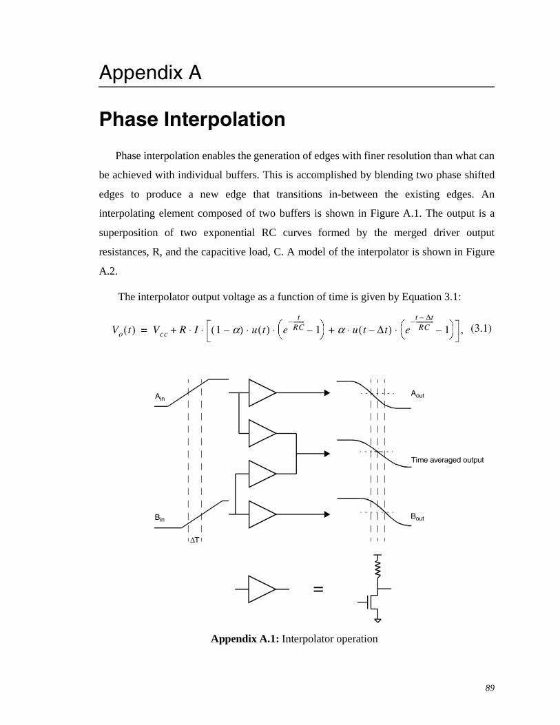
Appendix A: Phase Interpolation
89
Appendix A
Phase Interpolation
Phase interpolation enables the generation of edges with finer resolution than what can
be achieved with individual buffers. This is accomplished by blending two phase shifted
edges to produce a new edge that transitions in-between the existing edges. An
interpolating element composed of two buffers is shown in Figure A.1. The output is a
superposition of two exponential RC curves formed by the merged driver output
resistances, R, and the capacitive load, C. A model of the interpolator is shown in Figure
A.2.
The interpolator output voltage as a function of time is given by Equation 3.1:
∆T
Ain
Bin
Aout
Bout
Time averaged output
=
Appendix A.1: Interpolator operation
Vo t( ) Vcc R I 1 α–( ) u t( ) et
RC--------–
1– ⋅⋅ α u t ∆t–( ) e
t t∆–RC
-------------–1–
⋅ ⋅+ ,⋅ ⋅+= (3.1)

Appendix A: Phase Interpolation
90
where α is the ratio of the currents in the differential pairs, ∆t is the phase difference
between the inputs, I is the sum of the two tail currents and u(t) is the unit step function.
Because Vo(t) is a superposition of two time-shifted exponential waveforms, the
output phase does not vary linearly with the current ratio α. The amount of nonlinearity
depends on the ratio of the phase difference of the input signals, ∆t, and the output slew
rate, which is set by the time constant RC. Figure A.3 plots the output of the interpolator
for varying values of ∆t/RC. As the ∆t/RC ratio increases, slope of the output at midpoint
increases. Increased slope causes an increase in sensitivity of interpolation output phase to
CL
γ λ
(1-α)I αI
RS
Figure A.2: Interpolator model
0
0.2
0.4
0.6
0.8
1
0 0.2 0.4 0.6 0.8 1
Nor
mal
ized
out
put p
hase
Interpolator weight (α)
∆t/RC=0.5
∆t/RC=2
∆t/RC from 0.5 to 2 in linear steps
Figure A.3: Linearity of interpolator model with unit step inputs

Appendix A: Phase Interpolation
91
small variations in α.
According to this model, significant interpolation nonlinearities are avoided by
ensuring that the input phase spacing, ∆t, should be at most equal to the output RC time
constant. However, in practice, if the inputs are phase shifted by a buffer delay, the ratio of
∆t to RC is not significant. This contradicts the data shown in Figure A.3 because that plot
is generated assuming the inputs are step functions. A more reasonable assumption is that
the current waveform has a finite risetime, where risetime is measured 10%-90%, related
to the risetime of the input switching the current sources on. The simulated dependence of
the current risetime to the input risetime is shown in Figure A.4. This SPICE generated
plot shows that the current rise time is roughly approximated by risetime of the input
voltage. Input rise times ranging from one FO-4 delay to four FO-4 delays are plotted for
comparison.
Cur
rent
s (li
n)
0
50u
100u
150u
200u
250u
300u
350u
400u
450u
500u
550u
600u
650u
Vol
tage
s (li
n)
1
1.2
1.4
1.6
1.8
2
2.2
2.4
Time (lin) (TIME)4n 4.1n 4.2n 4.3n 4.4n 4.5n 4.6n 4.7n
*
Figure A.4: Interpolator current versus input rise time
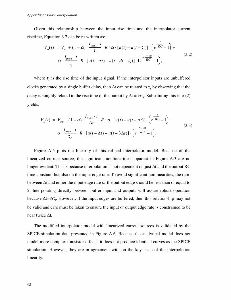
Appendix A: Phase Interpolation
92
Given this relationship between the input rise time and the interpolator current
risetime, Equation 3.2 can be re-written as:
where τr is the rise time of the input signal. If the interpolator inputs are unbuffered
clocks generated by a single buffer delay, then ∆t can be related to τr by observing that the
delay is roughly related to the rise time of the output by ∆t = ½τr. Substituting this into (2)
yields:
Figure A.5 plots the linearity of this refined interpolator model. Because of the
linearized current source, the significant nonlinearities apparent in Figure A.3 are no
longer evident. This is because interpolation is not dependent on just ∆t and the output RC
time constant, but also on the input edge rate. To avoid significant nonlinearities, the ratio
between ∆t and either the input edge rate or the output edge should be less than or equal to
2. Interpolating directly between buffer input and outputs will assure robust operation
because ∆t=½τr. However, if the input edges are buffered, then this relationship may not
be valid and care must be taken to ensure the input or output edge rate is constrained to be
near twice ∆t.
The modified interpolator model with linearized current sources is validated by the
SPICE simulation data presented in Figure A.6. Because the analytical model does not
model more complex transistor effects, it does not produce identical curves as the SPICE
simulation. However, they are in agreement with on the key issue of the interpolation
linearity.
Vo t( ) Vcc 1 α–( )Imax t⋅
τr
---------------- R α u t( ) u t τr–( )–[ ] et
RC--------–
1– ⋅ ⋅ ⋅ ⋅⋅
αImax t⋅
τr
---------------- R u t ∆t–( ) u t dt– τr–( )–[ ] et t∆–RC
-------------–1–
,⋅ ⋅ ⋅ ⋅
+ +=
(3.2)
Vo t( ) Vcc 1 α–( )Imax t⋅
∆t---------------- R α u t( ) u t ∆t–( )–[ ] e
tRC--------–
1– ⋅ ⋅ ⋅ ⋅⋅
αImax t⋅
τr
---------------- R u t ∆t–( ) u t 3∆t–( )–[ ] et t∆–RC
-------------–1–
.⋅ ⋅ ⋅ ⋅
+ +=(3.3)

Appendix A: Phase Interpolation
93
0
0.2
0.4
0.6
0.8
1
0 0.2 0.4 0.6 0.8 1
Nor
mal
ized
out
put p
hase
Interpolator weight (α)
∆t/RC=0.5
∆t/RC=2
∆t/RC from 0.5 to 2 in linear steps
Figure A.5: Linearity of interpolator model with finite risetime inputs
0
0.2
0.4
0.6
0.8
1
0 0.2 0.4 0.6 0.8 1
Nor
mal
ized
out
put p
hase
Interpolator weight (α)
∆t/RC=0.5
∆t/RC=2
∆t/RC from 0.5 to 2 in linear steps
Figure A.6: Linearity of interpolator SPICE model

Appendix A: Phase Interpolation
94
95
References
[1] J. Adler et. al. “Low Noise, Low Jitter Hybrid Ovenized SAW Oscillators,” Vec-tron International, 2000.
[2] T. Blalack, “Switching Noise in Mixed-Signal Integrated Circuits,” Ph.D. Disser-tation, Stanford University, 1997.
[3] S. Brown et. al. “A Gate-Array Based 500MHz Triple Channel ATE Controllerwith 40ps Timing Verniers,” MegaTest Corporation.
[4] Buihler, M., B. Blaes, H. Sayah, and U. Lieneweg, “Parameter Distributions forComplex VLSI Circuits,” Proc. of Decennial Conf. on VLSI, Mar. 1989, MITPress, pp 159-174.
[5] J. Bulaevsky et. al. “Partitioning Systems Designs - The tools and methodologiesMegatest used to develop the latest high-performance tester,” System Design,August 1996.
[6] J. Christiansen “An Integrated High Resolution CMOS Timing Generator Basedon an Array of Delay Locked Loops,” IEEE Journal of Solid State Circuits, vol.31, no. 7, pp. 952-957, July 1996.
[7] Will Creek, “Characterization of Edge Placement Accuracy in High-Speed DigitalPin Electronics,” International Test Conference, pp.556-557, Nov. 1993.
[8] Dally, William J., and Poulton, John W., Digital Systems Engineering, CambridgeUniversity Press, 1998.
[9] Dally, William J., and Poulton, John W., “High-Performance Signaling Systems,”Hot Interconnects, August 17, 1996.
[10] K. Donnelly et. al. “A 660 MB/s Interface Megacell Portable Circuit in 0.3µm-0.7µm CMOS ASIC,” IEEE Journal of Solid State Circuits, vol. 31, no. 12, pp.1995-2003, 1996.
[11] Forti, F. and M. Wright, “Measurement of MOS Current Mismatch in the WeakInversion Region,” IEEE Journal of Solid State Circuits, vol. 29, no. 2, pp. 138-142, 1994.
[12] J. Gasbarro et. al. “Integrated Pin Electronics for VLSI Functional Testers,” IEEEJournal of Solid State Circuits, vol. 24, no. 2, pp. 331-337, April 1989.
[13] J. Gasbarro and M. Horowitz, “Techniques for Characterizing DRAMs With a500MHz Interface,” International Test Conference, pp.516-525, Nov. 1994.
[14] A. Hajimiri and T. H. Lee, “A general theory of phase noise in electrical oscilla-tors,” IEEE Journal Solid-State Circuits, vol. 33, pp. 179–194, Feb. 1998.
[15] M. Horowitz, et. al., “High-speed electrical signalling: Overview and limitations,”IEEE Micro, vol. 18, no. 1, Jan.-Feb. 1998, pp.12-24.
96
[16] Huffman, D. A., “A Method for the Construction of Minimum-RedundancyCodes,” Proc. IRE, vol. 40, no. 9, pp. 1098-1101, Sept. 9, 1952.
[17] H. Johansson et. al. “Time Resolution of NMOS Sampling Switches Used on Low-Swing Signals,” IEEE Journal of Solid State Circuits, vol. 33, no. 2, pp. 237-245,1998.
[18] T. Knotts et. al., “A 500MHz Time Digitizer IC with 15.625ps Resolution,” Inter-national Solid-State Circuits Conference, 1994, pp. 58-59.
[19] Lakshmikumar, K., R. Hadaway, and M. Copeland, “Characterization of Modelingof Mismatch in MOS Transistors for Precision Analog Design,” IEEE JournalSolid-State Circuits, vol 21, no. 3, pp 1057-1066.
[20] T. Lee, The Design of CMOS Radio-Frequency Circuits, Cambridge UniversityPress, 1998.
[21] M. Li et. al. “A New Method for Jitter Decomposition Through Its DistributionTail Fitting,” Technical Bulletin, no. 9, 1999, Wavecrest Corporation.
[22] M. Loinaz, “Mixed-Signal VLSI Circuits for Particle Detector Instrumentation inHigh-Energy Physics Experiments,” Ph.D. Dissertation, Stanford University,1995.
[23] J. Maneatis et. al. “Precise Delay Generation Using Coupled Oscillators,” IEEEJournal of Solid State Circuits, vol. 28, no. 12, pp. 1273-1282, Dec. 1993.
[24] J. Maneatis, “Precise Delay Generation Using Coupled Oscillators,” Ph.D. Disser-tation, Stanford University, 1993.
[25] J. Maneatis et. al. “Low-jitter process-independent DLL and PLL based on self-biased techniques,” IEEE Journal of Solid State Circuits, vol. 31, no. 11, pp. 1723-1732, Nov. 1996.
[26] J. Miyamoto et. al. “A Single-Chip LSI High-Speed Functional Tester,” IEEEJournal of Solid State Circuits, vol. sc-22, no. 5, pp. 820-828, Oct. 1987.
[27] J. Montanaro et. al. “A 160-MHz, 32-b, 0.5W CMOS RISC Microprocessor,”IEEE Journal of Solid State Circuits, vol. 31, no. 11, pp. 1703-1714, Nov. 1996.
[28] G. Moyer et. al. “The Delay Vernier Pattern Generation Technique,” IEEE Journalof Solid State Circuits, vol. 32, no. 4, pp. 551-562, April 1997.
[29] F. Mu et. al. “Digital Multiphase Clock/Pattern Generator,” IEEE Journal of SolidState Circuits, vol. 34, no. 2, pp. 182-191, Feb. 1999.
[30] M. Pelgrom et. al., “Matching Properties of MOS Transistors,” IEEE Journal ofSolid State Circuits, vol. 24, no. 5, pp. 1433-1439, Oct. 1989.
[31] S. Sidiropoulos et. al. “A Semi-digital Dual Delay-Locked Loop,” IEEE Journal ofSolid State Circuits, vol. 32, no. 11, pp. 1683-1692, Nov. 1997.
[32] S. Sidiropoulos, “High Performance Inter-Chip Signalling,” Ph.D. Dissertation,Stanford University, 1998.

97
[33] M. Simpson et. al. “An Integrated CMOS Time Interval Measurement System withSub nanosecond Resolution for the WA-98 Calorimeter,” IEEE Journal of SolidState Circuits, vol. 32, no. 2, pp. 198-205, Feb. 1997.
[34] G. Wei et. al. “A Variable-Frequency Parallel I/O Interface with Adaptive Power-Supply Regulation,” IEEE Journal of Solid State Circuits, vol. 35, no. 11, pp.1600-1610, Nov. 2000.
[35] T. Welch, “A Technique for High-Performance Data Compression”, ComputerMagazine of the Computer Group News of the IEEE Computer Group Society, vol.17, no. 6, June 1984.
[36] C. Yang et. al. “A 0.8-µm CMOS 2.5 Gb/s Oversampling Receiver and Transmitterfor Serial Links,” IEEE Journal of Solid State Circuits, vol. 31, no.12, pp 2015-2023, Dec. 1996.
[37] C. Yang “Design of High-Speed Serial Links in CMOS,” Ph.D. Dissertation, Stan-ford University, 1999.
[38] M. Zargari et. al. “A BiCMOS Active Substrate Probe-Card Technology for Digi-tal Testing,” IEEE Journal of Solid State Circuits, vol. 34, no. 8, pp 1118-1135,Aug. 1999.
[39] J. Ziv, and A. Lempel, “A Universal Algorithm for Sequential Data Compression,”IEEE Trans. Inform. Theory, vol. 23, no. 3 pp. 337-343, May 1977.
[40] Ziv, J., and Lempel, A., “Compression of Individual Sequences via Variable-RateCoding,” IEEE Trans. Inform. Theory, vol. 24, no. 5, pp. 530-536, Sept. 1978.
[41] Aglient 95000 High Speed Memory Series Product Documentation, Aglient Inc.,2000.
[42] Draft AGP 3.0 Interface Specification, Intel Corporation, May 2001.
[43] Double Data Rate (DDR) SDRAM Specification, JEDEC Standard, Joint ElectronDevice Engineering Council, http://www.jedec.org/DOWNLOAD/jedec/JESD79R1.pdf.
[44] Rambus RIMM Module Data Sheet, Document DL0078, Rambus Inc., Mar. 1999.
[45] Texas Instruments TLK3101 Data Sheet, SCAS649A, Texas Instruments, http://www-s.ti.com/sc/psheets/scas649a/scas649a.pdf.
[46] Schlumberger EXA2000 Series Product Literature, Schlumberger Inc., 1999.

98