Embed Size (px)
Citation preview

Analog signal processing: blocks, trends and limitations
Ramon Pallàs-Areny, Manel GasullaInstrumentation, Sensors and Interfaces Group
Castelldefels School of TechnologyUniversitat Politècnica de Catalunya
Barcelona – Spainhttp://isi.upc.es
Our Campus!!Castelldefels (Barcelona), Spain

R. Pallàs-Areny, M. Gasulla Summer School-Benevento 2007 3
Index1. Function and structure of DAS2. Functions on signal amplitude, level and power3. Functions on signal spectrum: filtering4. Uncertainty and calibration5. Trends in AFE for DAS
Textbook:Analog Signal ProcessingR. Pallàs-Areny and J. G. WebsterNew York: John Wiley & Sons, 1999
R. Pallàs-Areny, M. Gasulla Summer School-Benevento 2007 4

R. Pallàs-Areny, M. Gasulla Summer School-Benevento 2007 5
Index
1. Function and structure of DAS2. Functions on signal amplitude, level and
power3. Functions on signal spectrum: filtering4. Uncertainty and calibration5. Trends in AFE for DAS
R. Pallàs-Areny, M. Gasulla Summer School-Benevento 2007 6
1. Functions and structure of DAS
1.1 Basic functions in measurement systems
1.2 Dynamic range: amplitude and level matching
1.3 Architectures for DAS

R. Pallàs-Areny, M. Gasulla Summer School-Benevento 2007 7
Basic functions in measurement systems
For any size or design scale
Sensing Processing Communication
Powersupply
Control/memory
R. Pallàs-Areny, M. Gasulla Summer School-Benevento 2007 8
Sensing
Primarysensor
Signalconverter
Sensing Processing Communication
Powersupply
Control/memory

R. Pallàs-Areny, M. Gasulla Summer School-Benevento 2007 9
Processing
ADCAnalogprocessing
Signal-to-symbolconverter
Sensing Processing Communication
Powersupply
Control/memory
R. Pallàs-Areny, M. Gasulla Summer School-Benevento 2007 10
Analog signal processingADCAnalog
processingSignal-to-symbol
converter
Sensorconditioner
Analogprocessor
Excitation/biasAmplificationLevel shiftingFilteringImpedance adaptation
DemodulationLinearizationCompression

R. Pallàs-Areny, M. Gasulla Summer School-Benevento 2007 11
Function types
1. Conversion: sensor, ADC, analog processor
2. Adaptation/matching: conditioner + analog processor
Amplitude: attenuator, amplifierLevel: level shifter (amplifier)Power: input/output protectionImpedanceBandwidth: filtersTerminals
Sensor AnalogprocessorConditioner
Dx voyMeasurand ADC
Excitation/bias
AFE
R. Pallàs-Areny, M. Gasulla Summer School-Benevento 2007 12
ADC: transfer characteristic
CAD
Vref
LSB
MSB
Vs+ Vs-
vxt1 t2 t3
01111010
t111100101
t211111111
t3
3Q 4Q 5Q 6Q 7Q vx
Codenumber
1
2
3
4
5
6
7
8
Intervalnumber
1 82 3 4 5 6 7
2QQ
vx
eQ
-Q/2
+Q/2
( )
= +
=
ir
ir ref
ent 2 1Nxx
VDV
V VQuantization intervalQ = Vref/2N = 1 LSB
eQ-Q/2 +Q/2
p(eQ)
Quantization noise:var [eQ] = Q2/12

R. Pallàs-Areny, M. Gasulla Summer School-Benevento 2007 13
QuantizationAnalogsignal Scale Code
transitionlevels
Codebin
Digitaloutput
ADC
FSR
0
T[2N-1] 2N-1
0
Vmax
Vmin000
111
100
Vx
T[k]k
[ ] ( ) [ ]= × − +1 1T k Q k T
T[1]
k-1
1 100
2N-2 110
011
Input
R. Pallàs-Areny, M. Gasulla Summer School-Benevento 2007 14
Resolution in ADCs
N 2N % ×10-6 dB 8 256 0,390 625 3 906,25 -48,2
10 1 024 0,097 656 976,56 -60,212 4 096 0,024 414 244,14 -72,214 16 384 0,006 104 61,04 -84,316 65 536 0,001 526 15,26 -96,318 262 144 0,000 381 3,81 -108,420 1 048 576 0,000 095 0,95 -120,422 4 194 304 0,000 024 0,24 -132,524 16 777 216 0,000 006 0,06 -144,5
R. Pallàs-Areny, M. Gasulla Summer School-Benevento 2007 15
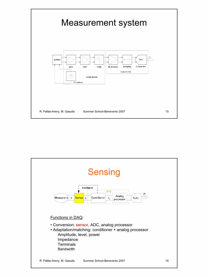
Measurement system
R. Pallàs-Areny, M. Gasulla Summer School-Benevento 2007 16
Sensing
Functions in DAQ:
• Conversion: sensor, ADC, analog processor• Adaptation/matching: conditioner + analog processor
Amplitude, level, powerImpedanceTerminalsBandwidth

R. Pallàs-Areny, M. Gasulla Summer School-Benevento 2007 17
What’s a sensor?
Materialproperties
Geometry
+Physical/chemicalquantity
Electricaloutput
Interfering quantity
Interfering quantity
R. Pallàs-Areny, M. Gasulla Summer School-Benevento 2007 18
Sensing methodsSensing: Transduction from non-electrical to electrical quantity1. Material-based sensing: conductors, semiconductors,
insulators, magnetic– Mechanical: piezoresistivity, piezoelectricity…– Thermal: Seebeck effect…– Magnetic: AMR, GMR, Hall effect…– Optical: photoelectric effect…– Chemical (concentration): Nernst equation…
2. Geometry-based sensors (linear or angular displacements):
– Potentiometer– Capacitive– Inductive– Mutual inductance

R. Pallàs-Areny, M. Gasulla Summer School-Benevento 2007 20
Sensor classification: power supply
Modulating sensorx y
Excitation
Modulating sensorx y
Excitation
Power flow
Electromagneticsensor
x y
Bias
Electromagneticsensor
x y
Bias
Power flow
Self-generatingsensor
x y Self-generatingsensor
x yPower flow
R. Pallàs-Areny, M. Gasulla Summer School-Benevento 2007 21
Sensor classification: output signalAnalogsensorx y
Quasi-digitalsensorx
y
Digitalsensorx 01101
y

R. Pallàs-Areny, M. Gasulla Summer School-Benevento 2007 23
Analog signal processing
Conditioner + analog processor functions:
• Sensor excitation (driving) or bias • Adaptation/matching:
Amplitude, level, powerImpedanceBandwidth (filtering)Terminals
• Analog signal processing:Domain conversion (I → V, ac → dc)LinearizationInterference compensation
Sensor AnalogprocessorConditioner
Dz voyMeasurand ADC
Excitation/bias
AFE
R. Pallàs-Areny, M. Gasulla Summer School-Benevento 2007 24
(1 - α)RT
VrαRT
ADC
RefD
Excitation/bias
( ) ( )s
r
2 1 2 1N NvD
Vα= − = −
Rin ADC >> RT
Potentiometer: ratiometric measurement
R
Rr
vo
Vr
Resistive sensors
ro
r
max r
Vv R
R RS R R
=+
⇒ =
vs
R. Pallàs-Areny, M. Gasulla Summer School-Benevento 2007 25
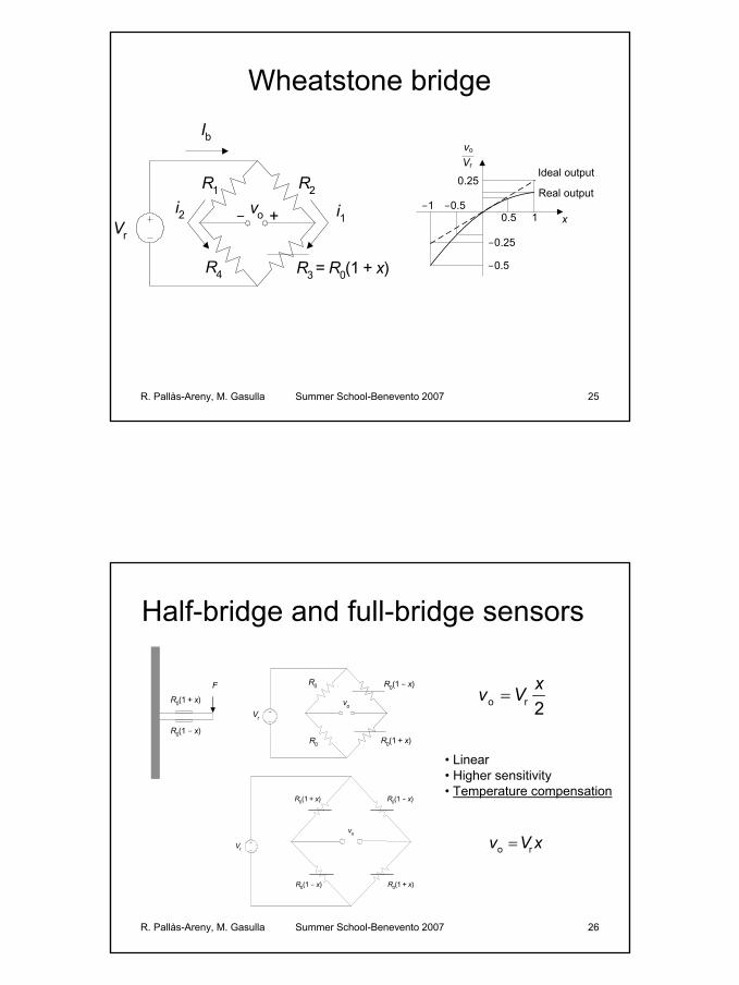
Wheatstone bridge
0.5 1-0.5-1
Ideal output
Real output0.25
vo
Vr
x
-0.5
-0.25Vr
R2
R3 = R0(1 + x)R4
R1
voi2 i1+-
Ib
R. Pallàs-Areny, M. Gasulla Summer School-Benevento 2007 26
o rv V x=
o r 2xv V=
Half-bridge and full-bridge sensors
R0(1 + x)
R0(1 - x)
F
Vr
R0(1 - x)
R0
R0
vo
R0(1 + x)
R0(1 + x)
R0(1 - x)
vo
R0(1 + x)
R0(1 - x)
Vr
• Linear• Higher sensitivity• Temperature compensation

R. Pallàs-Areny, M. Gasulla Summer School-Benevento 2007 27
Amplification
If Vo,max – Vo,minn ≤ Vin,max – Vin,minn+1 ⇒Range matching: amplification
Vs+
Vs-
vin vo
R. Pallàs-Areny, M. Gasulla Summer School-Benevento 2007 28
Amplification limits
Vout, max < Vs+Vout, min > Vs-
RRIRRO
G(f)
Vs+
Vs-
Vout,max
Vout,min
ZL
IL < Io,max
IL
Vin,max
Vin,min
Voltage headroom
IL comes from the power supply

R. Pallàs-Areny, M. Gasulla Summer School-Benevento 2007 29
Level shiftingWe need: Vo,minn = Vin,minn+1
Vo,maxn = Vin,maxn+1
Vref ≠ Vs
G
Vs+
Vs-
+
Vos = αVref
αGVref
R. Pallàs-Areny, M. Gasulla Summer School-Benevento 2007 30
Impedance adaptation/matching
1. Signal transfer (undesired attenuations): Vo→ VLIo→ IL
2. Signal integrity (when l > λ/10) ⇒ ZL = ZS
3. Maximal power transfer ⇒ ZL = Z*S
Zo
Vo ZLVL ZoIo ZLIL

R. Pallàs-Areny, M. Gasulla Summer School-Benevento 2007 31
Voltage loading effectZo
Vo Zi (ZD)Vi
ZLZL + Zi
A(f) =Source Load
Solution: voltage buffer (impedance transformer)
R. Pallàs-Areny, M. Gasulla Summer School-Benevento 2007 32
DC voltage divider effect
i i
o o i
V RV R R
=+
i o io o,FSR
o o
1If when 22
MM
V V RV VV R−
< = ⇒ >
Ro
vo vi Ri

R. Pallàs-Areny, M. Gasulla Summer School-Benevento 2007 33
AC voltage divider effect
( )( )
i0
i oi 0
eq io
eq o i 0 o
1
RAR R
V A R CV j
R R R A R
ωτ
ω ωτ
= += =+
= = ×
i oo o,FSR
o
20
If when
2 1 21 1
v vv V
v
A
ε
ε εωτε ε
−< =
+ −< ≈
− −max
eq i
1 22 1
fR C
επ ε
<−
Ro
vo vi Ri Ci
R. Pallàs-Areny, M. Gasulla Summer School-Benevento 2007 34
Maximal measurement frequencyε = 2-N 8 10 12 14 16 18 20 22fc/fmax 11.3 22.6 45.5 71 181 362 724 1448
lg f
A0
fc
0.7A0
A

R. Pallàs-Areny, M. Gasulla Summer School-Benevento 2007 35
1. A signal generator whose output resistance is 600 Ω is connected to a load resistance of 1 MΩ. Calculate the amplitude attenuation
2. A signal generator is connected to a 12 bit DAS whose input resistance is 1 MΩ. Calculate the maximal output resistance of the signal generator in order for it not to influence the measurement result
3. A grounded signal generator whose output resistance is 600 Ω is connected to an oscilloscope whose input impedance is 1 MΩ in parallel with 20 pF, using 2 m of a coaxial cable whose capacitance is 75 pF/m. If a maximal 0.1 % amplitude attenuation is accepted, what is the maximal signal frequency we can measure?
Examples
R. Pallàs-Areny, M. Gasulla Summer School-Benevento 2007 36
Bandwidth adaptation
( )
max min
c
c max min c max
max min
11
; often, , : depend on the application
f ff
f f f S f Sf f
>− <
= ≠
Signal bandwidth
Broadband signalNarrow band signal
f
S(f)
fcfmax fmin
S(f)
ffcfmax fmin

R. Pallàs-Areny, M. Gasulla Summer School-Benevento 2007 37
Circuit/system bandwidth
C H Lf f f=
|G|/|G0|
0 dB
fL fH lg ffc
3 dB< 3 dB
R. Pallàs-Areny, M. Gasulla Summer School-Benevento 2007 38
Bandwidth compatibility
Continuous signal systems: fL < fmin, fH > fmax
fL fH lg ffc
S(f),
fmaxfmin
|G|

R. Pallàs-Areny, M. Gasulla Summer School-Benevento 2007 39
Bandwidth compatibility
Sampled systems: fsampling/2 >”Signal BW”
R. Pallàs-Areny, M. Gasulla Summer School-Benevento 2007 40
DC and AC coupling
in,maxoff
min
vvkffc
<
<
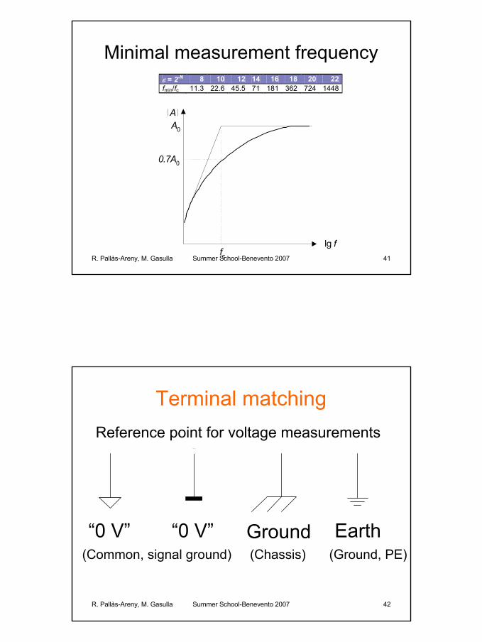
R. Pallàs-Areny, M. Gasulla Summer School-Benevento 2007 41
Minimal measurement frequencyε = 2-N 8 10 12 14 16 18 20 22fmin/fc 11.3 22.6 45.5 71 181 362 724 1448
lg f
A0
fc
0.7A0
A
R. Pallàs-Areny, M. Gasulla Summer School-Benevento 2007 42
Terminal matching
(Chassis) (Ground, PE)(Common, signal ground)
Reference point for voltage measurements

R. Pallàs-Areny, M. Gasulla Summer School-Benevento 2007 43
Single-ended voltages
(pseudo-differential)
=L "0 V"V
Floating
Zo
vo
Grounded
Zo
vo
Floating with a common-mode voltage
Zo
vo
vc Zc
R. Pallàs-Areny, M. Gasulla Summer School-Benevento 2007 44
Differential voltage, floatingvd = vH – vLvc = (vH + vL)/2
Z’o
Zo
Vd/2+
+Vd/2
H
L
C
vc Zc
Zo
Vd/2
Z’o
+
+Vd/2
H
L
C

R. Pallàs-Areny, M. Gasulla Summer School-Benevento 2007 45
Differential voltage, grounded
R. Pallàs-Areny, M. Gasulla Summer School-Benevento 2007 46
Differential voltage, generalZo
vd/2
Z’o
+
+vd/2
H
L
viso
Ziso
C
vc Zc
vc
vc
R. Pallàs-Areny, M. Gasulla Summer School-Benevento 2007 47
Single-ended input
Grounded Floating
R. Pallàs-Areny, M. Gasulla Summer School-Benevento 2007 48
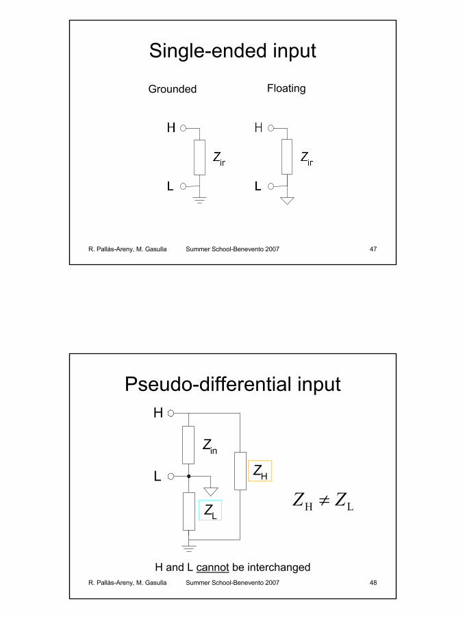
Pseudo-differential input
H and L cannot be interchanged
Zin
H
L
ZL
ZH
LH ZZ ≠

R. Pallàs-Areny, M. Gasulla Summer School-Benevento 2007 49
Differential input
Grounded Floating
H and L can be interchanged
ZD
H
L
ZC
ZC
COM
ZD
H
L
ZC
ZC
COM
ZISO
R. Pallàs-Areny, M. Gasulla Summer School-Benevento 2007 50
Example: pseudo-differential tosingle-ended conversion
R. Pallàs-Areny, M. Gasulla Summer School-Benevento 2007 51
1. Functions and structure of DAS
1.1 Basic functions in measurement systems1.2 Dynamic range: amplitude and level
matching1.3 Architectures for DAS
R. Pallàs-Areny, M. Gasulla Summer School-Benevento 2007 52
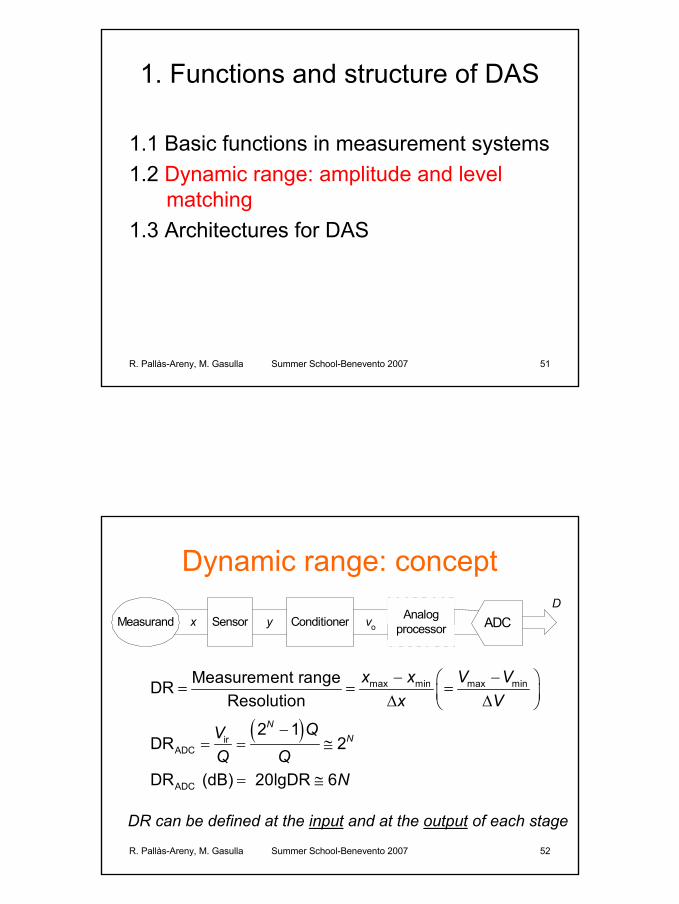
Dynamic range: concept
( )
max min max min
irADC
ADC
Measurement rangeDRResolution
2 1DR 2
DR (dB) 20lgDR 6
NN
x x V Vx V
QVQ Q
N
− − = = = ∆ ∆
−= = ≅
= ≅
Sensor Analog
processorConditionerD
x voyMeasurand ADC
DR can be defined at the input and at the output of each stage

R. Pallàs-Areny, M. Gasulla Summer School-Benevento 2007 53
Signal-to-noise ratio (SNR)
( )
2s2n
2s s s2n n n
Signal powerSNRNoise power
S/N dB 10lg 20lg 20lgσ
Ψ=
Ψ
Ψ Ψ Ψ= = =
Ψ Ψ
( ) ( ) ( )H
L
2 2 2 2
0 0
1limT f
x x x fTx t dt S f df S f df
Tµ σ
∞
→∞Ψ = = + = ≈∫ ∫ ∫
R. Pallàs-Areny, M. Gasulla Summer School-Benevento 2007 56
Application to system design
−=
−max min
max min
y ySx x
MR: xmax - xminResolution: ∆xDR = (xmax-xmin)/∆x
Sensor sensitivity (linear)−
=−
o,max o,min
max min
v vS
x x
System sensitivity (linear)
Sensor Analog
processorConditionerD
x voyMeasurand ADC
Procedure:1. Calculate DR from problem specifications2. Determine N for ADC3. Select a sensor that fulfills the design requirements4. Select/design a signal conditioner to match the output voltage
range of the sensor to the input voltage range of the ADC
R. Pallàs-Areny, M. Gasulla Summer School-Benevento 2007 57
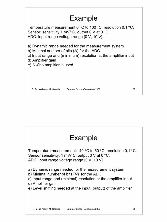
ExampleTemperature measurement 0 °C to 100 °C, resolution 0.1 °C.Sensor: sensitivity 1 mV/°C, output 0 V at 0 °C.ADC: input range voltage range [0 V, 10 V].
a) Dynamic range needed for the measurement systemb) Minimal number of bits (N) for the ADCc) Input range and (minimum) resolution at the amplifier inputd) Amplifier gaine) N if no amplifier is used
R. Pallàs-Areny, M. Gasulla Summer School-Benevento 2007 58
ExampleTemperature measurement: -40 °C to 60 °C, resolution 0.1 °C. Sensor sensitivity: 1 mV/°C, output 0 V at 0 °C.ADC: input range voltage range [0 V, 10 V].
a) Dynamic range needed for the measurement systemb) Minimal number of bits (N) for the ADCc) Input range and (minimal) resolution at the amplifier inputd) Amplifier gaine) Level shifting needed at the input (output) of the amplifier

R. Pallàs-Areny, M. Gasulla Summer School-Benevento 2007 59
Amplification and level shifting circuits
-+
R2R1
vo
R3
vs
voff
-+
R2R1
vo
R3
vs
voff
Non-inverter with level shifting Inverter with level shifting
213 RRR =
off1
2s
1
2o 1 v
RRv
RRv −
+= off
1
2s
1
2o 1 v
RRv
RRv
++−=
R. Pallàs-Areny, M. Gasulla Summer School-Benevento 2007 60
Differential amplifier with level shifting
vs2
vs1
vo
R3 R4
R4R3
-+
voff
( ) offs1s23
4o vvvRRv +−=

R. Pallàs-Areny, M. Gasulla Summer School-Benevento 2007 61
1. Functions and structure of DAS
1.1 Basic functions in measurement systems1.2 Dynamic range: amplitude and level
matching1.3 Architectures for DAS
R. Pallàs-Areny, M. Gasulla Summer School-Benevento 2007 62
Basic parameters for DAS (1)1. Functions:
– ADC– DAC– Digital I/O– PWM output– Specific sensor conditioners– Isolation– Event counters– Timers– Triggers
R. Pallàs-Areny, M. Gasulla Summer School-Benevento 2007 63
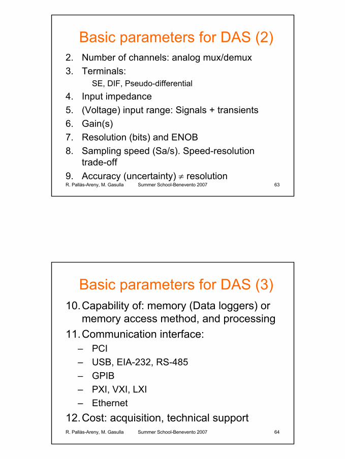
Basic parameters for DAS (2)2. Number of channels: analog mux/demux3. Terminals:
SE, DIF, Pseudo-differential4. Input impedance5. (Voltage) input range: Signals + transients6. Gain(s)7. Resolution (bits) and ENOB8. Sampling speed (Sa/s). Speed-resolution
trade-off9. Accuracy (uncertainty) ≠ resolution
R. Pallàs-Areny, M. Gasulla Summer School-Benevento 2007 64
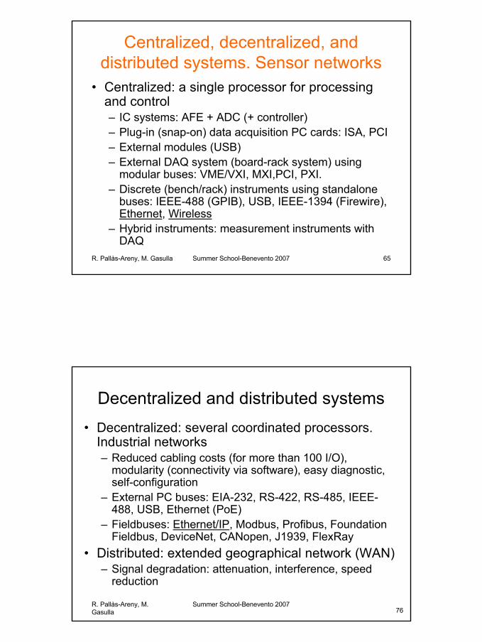
Basic parameters for DAS (3)10.Capability of: memory (Data loggers) or
memory access method, and processing11.Communication interface:
– PCI– USB, EIA-232, RS-485– GPIB– PXI, VXI, LXI– Ethernet
12.Cost: acquisition, technical support
R. Pallàs-Areny, M. Gasulla Summer School-Benevento 2007 65
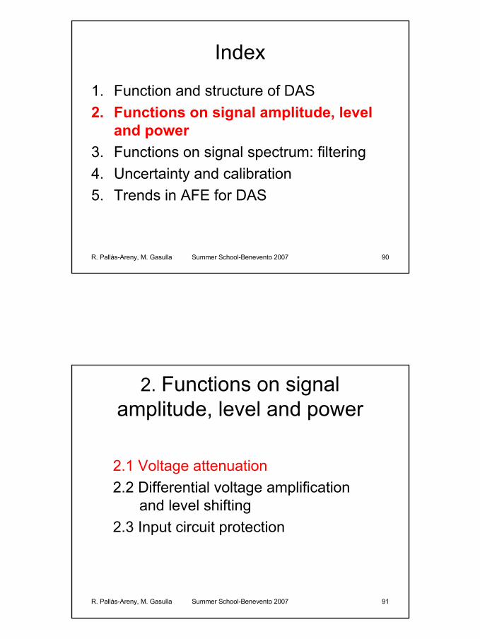
Centralized, decentralized, and distributed systems. Sensor networks
• Centralized: a single processor for processing and control– IC systems: AFE + ADC (+ controller)– Plug-in (snap-on) data acquisition PC cards: ISA, PCI– External modules (USB)– External DAQ system (board-rack system) using
modular buses: VME/VXI, MXI,PCI, PXI. – Discrete (bench/rack) instruments using standalone
buses: IEEE-488 (GPIB), USB, IEEE-1394 (Firewire), Ethernet, Wireless
– Hybrid instruments: measurement instruments with DAQ
R. Pallàs-Areny, M. Gasulla
Summer School-Benevento 200776
Decentralized and distributed systems• Decentralized: several coordinated processors.
Industrial networks– Reduced cabling costs (for more than 100 I/O),
modularity (connectivity via software), easy diagnostic, self-configuration
– External PC buses: EIA-232, RS-422, RS-485, IEEE-488, USB, Ethernet (PoE)
– Fieldbuses: Ethernet/IP, Modbus, Profibus, Foundation Fieldbus, DeviceNet, CANopen, J1939, FlexRay
• Distributed: extended geographical network (WAN)– Signal degradation: attenuation, interference, speed
reduction

R. Pallàs-Areny, M. Gasulla
Summer School-Benevento 200780
Ad-hoc wireless sensor networks (WSN)
1. Self-organizing: rapid deployment and reconfiguration → temporary networks
2. Cooperating nodes within communication range from each other
3. Energy efficiency: multi-hop routing informationRobust to node failureHigh-level of fault tolerance
R. Pallàs-Areny, M. Gasulla
Summer School-Benevento 200782
REALnet: WSN for environmental monitoring
Punt de mesura
Repetidor
Laboratori 123P
Punt de mesura
Repetidor
Laboratori 123P
Punt de mesura
Farola
Punt de mesura
Farola
PFC Joan AlbesaFebruary 2007

R. Pallàs-Areny, M. Gasulla
Summer School-Benevento 200783
Low-level and high-level multiplexingLow-level multiplexingSensor
1
Sensorn
Sensor2
AMUX SHALPF
Digitalcontroller
Systembus
ADCPGA
R. Pallàs-Areny, M. Gasulla
Summer School-Benevento 200784
High-level multiplexing
Sensor
Sensor
Sensor
AMUX SHALPF
Digital
LPF
LPF
LPF
ADC
Sensor1
Sensorn
Sensor2
AMUX SHALPF
Digitalcontroller
LPF
LPF
LPF
ADC
Systembus
Systembus
PGA
G = 1, 2, 4, 8G = 1, 2, 5, 10

R. Pallàs-Areny, M. Gasulla
Summer School-Benevento 200785
Simultaneous samplingSensor
1
Sensorn
Sensor2
LPF
LPF
LPF
SHA
MUX
SHA
SHA Digitalcontroller
Systembus
LPF ADC
R. Pallàs-Areny, M. Gasulla
Summer School-Benevento 200787
(Inherent) digital multiplexingSensor
1
Sensorn
Digitalcontroller
Systembus
LPF
LPF
SHA
SHA
Digitalcontroller
ADC
ADC
Smart sensors: IEEE 1451.X
R. Pallàs-Areny, M. Gasulla Summer School-Benevento 2007 90
Index
1. Function and structure of DAS2. Functions on signal amplitude, level
and power3. Functions on signal spectrum: filtering4. Uncertainty and calibration5. Trends in AFE for DAS
R. Pallàs-Areny, M. Gasulla Summer School-Benevento 2007 91
2. Functions on signal amplitude, level and power
2.1 Voltage attenuation2.2 Differential voltage amplification
and level shifting2.3 Input circuit protection

R. Pallàs-Areny, M. Gasulla Summer School-Benevento 2007 92
Voltage attenuation
2 i 2
o 1 2 i 1 2
in 1 2 i
Z Z ZAZ Z Z Z Z Z
Z Z Z Z
= ≈+ + +
= +
o in
i 2
Z ZZ Z
<<
>>
Zo
vo
Zivi
Z1
Z2
Zin
A : attenuator “gain”“Attenuation” : 1 - A
R. Pallàs-Areny, M. Gasulla Summer School-Benevento 2007 93
DC voltage attenuator
2 i 2
o 1 2 i 1 2
in 1 2 i
R R RAR R R R R R
R R R R
= ≈+ + +
= +vo
vi
RinRo
R1
R2 Ri

R. Pallàs-Areny, M. Gasulla Summer School-Benevento 2007 94
AC voltage attenuator
( )
( ) ( )
1 1 2 i i
eq 2 i
1 eq 1 2 i
in 1 2 i 1 i
Compensation:
o
R C R R C
Z R RA
Z Z Z R R R
Z R R R C C
=
= ≈+ + +
= + ⊕
Zo
vo
vi
Zin
R1
R2 Ri
C1
Ci
R. Pallàs-Areny, M. Gasulla Summer School-Benevento 2007 95
AC voltage attenuator (2)
( ) ( )
1 1 i i
eq i
1 eq 1 i
in 1 i 1 i
Compensation:
o
R C RCZ RA
Z Z Z R R
Z R R C C
=
= ≈+ + +
= + ⊕
Zo
vo
vi
Zin
R1
Ri
C1
Ci Useful for “small” Ri

R. Pallàs-Areny, M. Gasulla Summer School-Benevento 2007 96
Frequency-compensated attenuator
Vo CinCc Rin
Vin
Ro
Vo CinCc
Rin
Vin
R
9 MΩ
1 MΩC
Ro
Passive oscilloscope probe (1:10)
R. Pallàs-Areny, M. Gasulla Summer School-Benevento 2007 97
Attenuator adjustment
1 kHz

R. Pallàs-Areny, M. Gasulla Summer School-Benevento 2007 100
2. Functions on signal amplitude, level and power
2.1 Voltage attenuation2.2 Differential voltage amplification
and level shifting2.3 Input circuit protection
R. Pallàs-Areny, M. Gasulla Summer School-Benevento 2007 101
Fully-differential amplifier
iD iH iL
iH iLiC
oDoH oC
oDoL oC
2
2
2
v v vv vv
vv v
vv v
= − +
= = + = −
ic iD
ic iD
oD oCDD CC
iD iC0 0
oC oDCD DC
iD iC0 0
v v
v v
V VG GV V
V VG GV V
= =
= =
= =
= =

R. Pallàs-Areny, M. Gasulla Summer School-Benevento 2007 102
Ideal differential amplifier
oD DD iD DC iC DD iD
oC CD iD CC iC CC iC
DC
CD
DD
CC
0 Ideal
0
Discrimination factor: 1
V G V G V G VV G V G V G V
GG
GDG
= + = = + =
= =
= >>
R. Pallàs-Areny, M. Gasulla Summer School-Benevento 2007 103
Figures of merit
( )
( )
DD
DC
CD
DD
iCoD DD iD DC iC DD iD
oC CD iD CC iC CC iC iD
CMRR
Gf CG
GEG
VV G V G V G VC
V G V G V G V V ED
= =
=
= + = +
= + = +
R. Pallàs-Areny, M. Gasulla Summer School-Benevento 2007 104
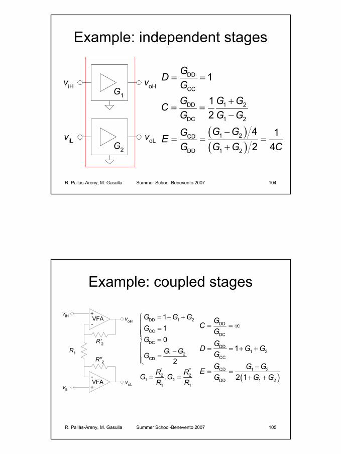
Example: independent stages
voH
voLG2
G1
viH
viL( )( )
DD
CC
DD 1 2
DC 1 2
1 2CD
DD 1 2
1
12
4 12 4
GDGG G GCG G G
G GGEG G G C
= =
+= =
−
−= = =
+
R. Pallàs-Areny, M. Gasulla Summer School-Benevento 2007 105
Example: coupled stages
DD 1 2
CC
DC
1 2CD
' "2 2
1 21 1
110
2
,
G G GGG
G GG
R RG GR R
= + + = =
− =
= = ( )
DD
DC
DD1 2
CC
CD 1 2
DD 1 2
1
2 1
GCGGD G GGG G GEG G G
= = ∞
= = + +
−= =
+ +viL
viH voH
voL
R'2
R''2
R1
-
+VFA
-
+VFA

R. Pallàs-Areny, M. Gasulla Summer School-Benevento 2007 106
Input impedances
voH
voL
vc vd/2
vd/2+
+
Zo
Z'o
ZD
L
H
ZC
Z'C
viH
viL
GCC
GDC
GCD
GDD
R. Pallàs-Areny, M. Gasulla Summer School-Benevento 2007 107
Input impedances: differentialZC → ∞

R. Pallàs-Areny, M. Gasulla Summer School-Benevento 2007 108
Input impedances: common mode
voH
voL
vc vd/2
vd/2+
+
Zo
Z'o
ZD
L
H
ZC
Z'C
viH
viL
GCC
GDC
GCD
GDD
R. Pallàs-Areny, M. Gasulla Summer School-Benevento 2007 109
Input impedances: common mode
voH
voL
vc vd/2
vd/2+
+
Zo
Z'o L
H
ZC
Z'C
viH
viL
GCC
GDC
GCD
GDD
A
B

R. Pallàs-Areny, M. Gasulla Summer School-Benevento 2007 110
Effect of common-mode input impedances
viH
viL
Z o
Z'o
Z C
Z'C
B
A
C oC Ca o oa
' 'C oC oa o oa
2 2
2 2
Z ZZ Z Z Z
Z ZZ Z Z Z
∆ ∆= + = +
∆ ∆= − = −
R. Pallàs-Areny, M. Gasulla Summer School-Benevento 2007 111
Effective CMRR( ) ( )
( )
( )
' 'C C o C C o Ca
iC ooa C Ca o oa
Ca oa
DD DDi DC CDie -1 -1
DD DCi DC CCi i a i a
12
1 14
Z Z Z Z Z Z ZC Z ZZ Z Z Z ZZ Z
G G G GCG G G G C C C C
+ + += ≅
∆ ∆∆ − ∆ −
+= = +
+ + +
A finite ZD does not affect this result
e i a
1 1 1C C C
≅ +

R. Pallàs-Areny, M. Gasulla Summer School-Benevento 2007 112
Cascade differential amplifiers
1T
1
1 1CMRR CMRR
CMRR
n
i ij i
i i jj
C D
=
<
=
≅
=
∑
∏
R. Pallàs-Areny, M. Gasulla Summer School-Benevento 2007 113
Additional errors: instrumentation amplifier
vo-
+IA
vL
vH
Ref
Don’t use “dc blocking” capacitors!
vc vd/2
vd/2
+
VioZo
Z'o
Ip
In
Vs+
Vs-
+vo
-
+IA
Ref
ZD
'onopioIZE RIRIV −+=

R. Pallàs-Areny, M. Gasulla Summer School-Benevento 2007 114
Instrumentation amplifier: deviations
( )o ref H L DDV V V V G− = −
( ) c s+ s-d ni
e + -
e front IA
1 IZE " "CMRR PSRR PSRR
1 1 1CMRR CMRR CMRR
o Gv V Vv G v Eε
∆ ∆= + + + + + +
= +
R. Pallàs-Areny, M. Gasulla Summer School-Benevento 2007 115
Instrumentation amplifier: frequency response
vo-
+IA
vL
vH
Ref
f 'af ''a fa
lg f
G
G''0
G0
G'0
( )
( )
o ref H L DD
0 aH L
a
V V V V GG fV Vjf f
− = −
= −+

R. Pallàs-Areny, M. Gasulla Summer School-Benevento 2007 116
DC level shifters
R
-
+Vs-
Vs+
VFA
Vs+
VrefIo
1ref 0
1 2
RV VR R
=+
R. Pallàs-Areny, M. Gasulla Summer School-Benevento 2007 118
2. Functions on signal amplitude, level and power
2.1 Voltage attenuation2.2 Differential voltage amplification
and level shifting2.3 Input circuit protection

R. Pallàs-Areny, M. Gasulla Summer School-Benevento 2007 119
Input circuit protection
Devicesto be
protected
Overcurrentprotection
Ove
rvol
tage
prot
ectio
n
R. Pallàs-Areny, M. Gasulla Summer School-Benevento 2007 120
Overvoltage protection
• Problems:– Damaged pn junctions by excessive reverse voltage– Dielectrics breakdown– Overcurrents– Circuit malfunctioning
• Solution: voltage transient suppressors– Transient attenuators: passive low-pass filters– Transient diverters:
• Voltage clamping devices: MOV, Transzorb®, Zener diodes• Foldback/crowbar circuits: GDT
R. Pallàs-Areny, M. Gasulla Summer School-Benevento 2007 121
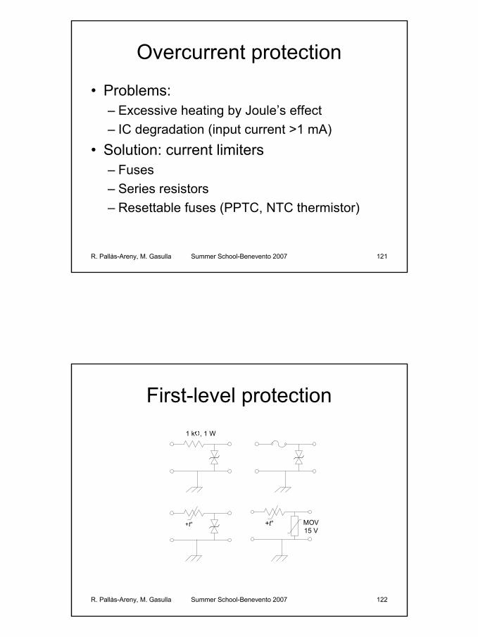
Overcurrent protection
• Problems:– Excessive heating by Joule’s effect– IC degradation (input current >1 mA)
• Solution: current limiters– Fuses– Series resistors– Resettable fuses (PPTC, NTC thermistor)
R. Pallàs-Areny, M. Gasulla Summer School-Benevento 2007 122
First-level protection1 k , 1 W
+t° +t° MOV15 V
R. Pallàs-Areny, M. Gasulla Summer School-Benevento 2007 123
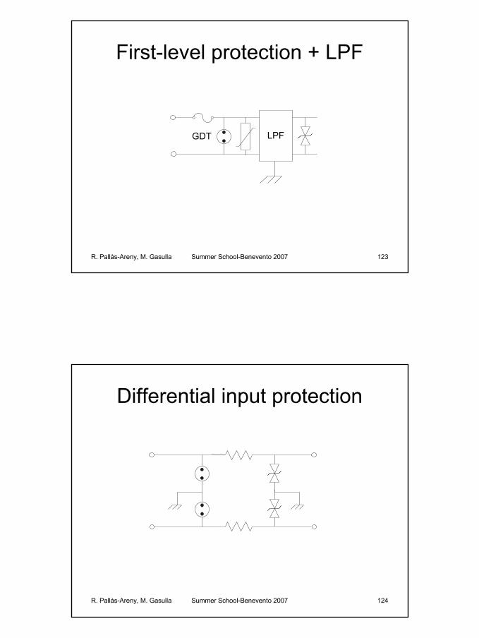
First-level protection + LPF
LPFGDT
R. Pallàs-Areny, M. Gasulla Summer School-Benevento 2007 124
Differential input protection
R. Pallàs-Areny, M. Gasulla Summer School-Benevento 2007 125
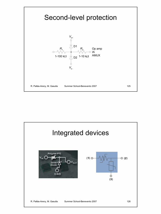
Second-level protection
R2
Vs-
Vs+
R1
D1
D21-100 k 1-10 k
Op ampIAAMUX
R. Pallàs-Areny, M. Gasulla Summer School-Benevento 2007 126
Integrated devices
R. Pallàs-Areny, M. Gasulla Summer School-Benevento 2007 128
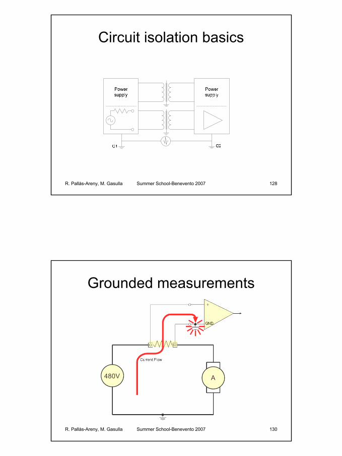
Circuit isolation basics
R. Pallàs-Areny, M. Gasulla Summer School-Benevento 2007 130
Grounded measurements
R. Pallàs-Areny, M. Gasulla Summer School-Benevento 2007 131
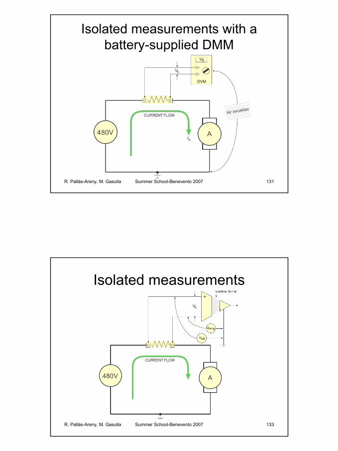
Isolated measurements with a battery-supplied DMM
R. Pallàs-Areny, M. Gasulla Summer School-Benevento 2007 133
Isolated measurements
R. Pallàs-Areny, M. Gasulla Summer School-Benevento 2007 134
Isolated USB DAQ module
R. Pallàs-Areny, M. Gasulla Summer School-Benevento 2007 145
Summary
1. Compensate ac attenuators2. Use differential amps whenever possible3. Beware of unexpected ac attenuations4. Keep differential circuits balanced5. Ensure input protection6. Consider isolation in industrial settings

R. Pallàs-Areny, M. Gasulla Summer School-Benevento 2007 146
Index
1. Function and structure of DAS2. Functions on signal amplitude, level and
power3. Functions on signal spectrum:
filtering4. Uncertainty and calibration5. Trends in AFE for DAS
R. Pallàs-Areny, M. Gasulla Summer School-Benevento 2007 147
3. Functions on signal spectrum: filtering
3.1 Frequency filtering fundamentals3.2 Differential filters

R. Pallàs-Areny, M. Gasulla Summer School-Benevento 2007 148
Filtering
• Linear filters discriminate signals based on their frequency.
• Used for:– Antialias filters– Interference and noise reduction
• Design of filters:– Approximation problem: filter shape– Realization problem: circuit implementation
R. Pallàs-Areny, M. Gasulla Summer School-Benevento 2007 149
Antialias filters
Source: IEEE Instrumentation & Measurement Magazine, October 2005
R. Pallàs-Areny, M. Gasulla Summer School-Benevento 2007 150
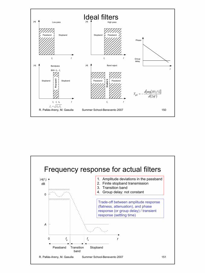
Ideal filters
f
Phase
Groupdelay
|H|
ffc
Passband Stopband
Low pass |H|
ffc
PassbandStopband
High pass
|H|
ffcfL fH
StopbandStopband
BW= fH - fL
Bandpass
LHc fff =
|H|
ffc
Passband Passband
Band reject
[ ]( )fd
fHdT
π2)(arg
gd −=
R. Pallàs-Areny, M. Gasulla Summer School-Benevento 2007 151
Frequency response for actual filters1. Amplitude deviations in the passband2. Finite stopband transmission3. Transition band4. Group delay: not constant
Trade-off between amplitude response (flatness, attenuation), and phase response (or group delay) / transient response (settling time)
fp f
dB
0
A
0 fs
Passband Transitionband
Stopband
H(f )

R. Pallàs-Areny, M. Gasulla Summer School-Benevento 2007 152
Frequency response
( ) A jBH fC jD
+=
+
2 22
2 2( ) A BH fC D
+=
+
arg ( ) arctan arctanB DH fA C
= −
( )gd
arg ( )2
d H fT
d fπ = −
R. Pallàs-Areny, M. Gasulla Summer School-Benevento 2007 153
Butterworth LPF
( )2
2c
1( )1 nH f
f f=
+
c
arg ( ) arctann
fH ff
= −

R. Pallàs-Areny, M. Gasulla Summer School-Benevento 2007 156
Chebyshev LPF
2
2 2c
1( )1 n
H fC f fε
=+
( ) ( )2dB 10lg 1R ε= +
R. Pallàs-Areny, M. Gasulla Summer School-Benevento 2007 159
Bessel filters: attenuation

R. Pallàs-Areny, M. Gasulla Summer School-Benevento 2007 162
Analog LPF: amplitude response
R. Pallàs-Areny, M. Gasulla Summer School-Benevento 2007 163
Analog LPF: group delay

R. Pallàs-Areny, M. Gasulla Summer School-Benevento 2007 164
Analog LPF: step response
R. Pallàs-Areny, M. Gasulla Summer School-Benevento 2007 165
Comparative• Bessel:
– Excellent step response (low distorsion)– Bad flatness and attenuation– Use where transient response is important
• Chevyshev:– Good attenuation– Ripple in pass-band and ringing in step response– Steeper attenuation at the cost of more passband
ripple (ε↑).• Butterworth:
– Good compromise between all parameters. – Good first choice general purpose filter

R. Pallàs-Areny, M. Gasulla Summer School-Benevento 2007 169
Circuit topologiesFirst-order (n=1) and second-order (n=2), low-pass RC passive filters
Second-order (n=2), low-pass active filters
VCVS, Sallen-KeyMultiple feedback (MFB)
R. Pallàs-Areny, M. Gasulla Summer School-Benevento 2007 170
Cascading of basic blocs

R. Pallàs-Areny, M. Gasulla Summer School-Benevento 2007 171
Filter design1. Determine design requirements: amplitude, group delay
(phase linearity), transient response2. Select an appropriate transfer function (approximation
problem): Butterworth, Chebyschev, Bessel…3. Determine filter order (n) from graphics, tables,
equations…4. Filter implementation (realization problem, filter
synthesis) ⇒ circuit topology: passive/active, Sallen-Key (VCVS, MFB,…), biquad, state variable…
5. Circuit design: use appropriate software from IC manufacturers (FilterCAD®, Filterlab®, FilterPro®, FilterWizard®…)
R. Pallàs-Areny, M. Gasulla Summer School-Benevento 2007 172
Noise bandwidth
( ) 2
2 00
1B G f dfG
∞= ∫
( )
c
H L
-3 dB
-3 dB3
LPF-1:2
BPF-1: 2
LPF-2: 1.224 2 1
3LPF-3: 1.1516 2 1
B f
B f f
B f
B f
π
π
π
π
=
= +
= ≈−
= ≈−
R. Pallàs-Areny, M. Gasulla Summer School-Benevento 2007 173
3. Functions on signal spectrum: filtering
3.1 Frequency filtering fundamentals3.2 Differential filters
R. Pallàs-Areny, M. Gasulla Summer School-Benevento 2007 174
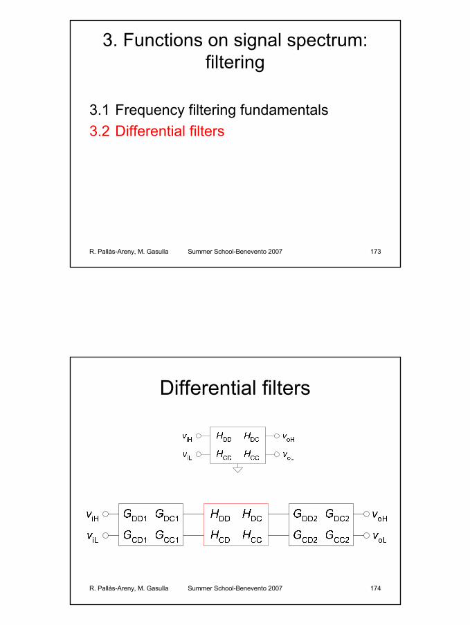
Differential filters

R. Pallàs-Areny, M. Gasulla Summer School-Benevento 2007 175
Differential filters: independent stages
( ) ( ) ( )( ) ( )
1 2
1 2
1CMRR2
H jf H jfjf
H jf H jf+
=−
R. Pallàs-Areny, M. Gasulla Summer School-Benevento 2007 176
Bad differential passive filter
voHviH
voLviL
R1
R'1
C1
C'1
( ) ( )( )
'
1 ' 11CMRR '2 '
'Example:
0.01, 0.05
CMRR = 60 dB 0.01
R C
R C
R C
t t ss
t t ss sRC
t t
RCω ω
+ +=
+
=
= =
⇒ = =

R. Pallàs-Areny, M. Gasulla Summer School-Benevento 2007 177
Bad input ac coupling
R. Pallàs-Areny, M. Gasulla Summer School-Benevento 2007 178
Differential filters: coupled stages
( )CMRR jf = ∞
R. Pallàs-Areny, M. Gasulla Summer School-Benevento 2007 179
Differential LP passive filter
voHviH
voLviL
R1
R'1
C1
C'1 ( )oH oL
'' 1 1iH iL
1 1 '1 1
1
1
v vC Cv v s R R
C C
−=
−+ +
+
( )CMRR jf = ∞
R. Pallàs-Areny, M. Gasulla Summer School-Benevento 2007 180
Input RFI filter
( )c '0 0
12
fR R Cπ
=+

R. Pallàs-Areny, M. Gasulla Summer School-Benevento 2007 181
Differential HP filter: coupled stages + bias network
( )1a 2 1a2 2CMRR
R C
j f R R Ct t
π +≈
+
R. Pallàs-Areny, M. Gasulla Summer School-Benevento 2007 182
Differential ac coupling
v1
vo
R1
C1
-
+IA
v2
R'1
C'1
R2
( )1a 2 1ai
2π 2
R C
j f R R CC
t t+
≈+
e i IA
1 1 1C C C
= +
L ' '' 1 1 1 1
1 1 '2 1 1
TH
1
2πf
R R C CR RR C C
ffG
=
+ + +
=

R. Pallàs-Areny, M. Gasulla Summer School-Benevento 2007 183
Differential ac coupling network
( )( )
'2 2oH oL
'iH iL 2 2 1
s R R Cv vv v s R R C
+−=
− + +
C
R2
R'2
C
R1
R'1
viH
viL
voH
voL
( )CMRR jf = ∞
R. Pallàs-Areny, M. Gasulla Summer School-Benevento 2007 184
Differential ac coupling
e i IA
1 1 1C C C
= +
( )L '
' 1 12 2 '
1 1
TH
1
2πf
C CR RC C
ffG
=+
+
=

R. Pallàs-Areny, M. Gasulla Summer School-Benevento 2007 185
Active LP differential filter
+
-
47 nF
39.2 kΩ 280 kΩ
+
-
4.7 nF
47 nF
39.2 kΩ 280 kΩ
Low-pass, 2nd order, Butterworth, BW: 70 Hz
R. Pallàs-Areny, M. Gasulla Summer School-Benevento 2007 186
Summary
1. Filter selection: attenuation, ripple, group delay and transient response
2. Avoid non-coupled differential filters3. Don’t forget input currents4. Reduce differential input impedances as
much as feasible5. Reduce bandwidth as much as possible

R. Pallàs-Areny, M. Gasulla Summer School-Benevento 2007 187
Index
1. Function and structure of DAS2. Functions on signal amplitude, level and
power3. Functions on signal spectrum: filtering4. Uncertainty and calibration5. Trends in AFE for DAS
R. Pallàs-Areny, M. Gasulla Summer School-Benevento 2007 188
Uncertainty sources
• Systematic effects– Offset (voltage, bias and leakage currents)– Component tolerance– Temperature coefficients (θ measurement)– Reduction: static calibration
• Random effects– Noise– Interference– Environmental noise (pseudonoise)

R. Pallàs-Areny, M. Gasulla Summer School-Benevento 2007 189
Accuracy → Uncertainty
Measurand (Result of a) measurement[Ma, Mb] Instrument loading [Va, Vb] M = V ± U [M]- Undisturbed value V: measured value (central)
- Intrinsic uncertainty U: uncertainty (dispersion)Confidence level: 95 %
Alternative method:• Standard uncertainty: u = σ(v)• Uncertainty: U = k×u; k = coverage factor (k = 2 →95.42 %)
R. Pallàs-Areny, M. Gasulla Summer School-Benevento 2007 190
Calibration diagram and curve
Vi: measured valueUi: intrinsic uncertainty (instrument)
Alternatives to calibration diagrams:- Calibration table- Algebraic equation
Sensitivity (linear): RSV
∆=
∆
Readings or indicationsin output units
R
Mea
sure
d va
lues
, in
mea
sure
men
t uni
ts
M
∆Rj
Vj
Ri
ViUiUi
Calibrationcurve
Calibration diagram
Reference conditions
Vj: conventional “true” valueUj < 0.1Ui
R. Pallàs-Areny, M. Gasulla Summer School-Benevento 2007 191
Uncertainty of measurement
InstrumentMeasurand[Interval]
Calibration curve
Calibrationdiagram
Reading
R
V
U
Indicatedvalue
UncertaintyMeasurement span Uncertainty limits
Operation conditions
M = V ± UResult
Influence quantities
Influence coefficients
R. Pallàs-Areny, M. Gasulla Summer School-Benevento 2007 192
Uncertainty limits
• (Absolute) uncertainty:U = a × R + AU = a × R + b × Vf Vf: fiducial value
• Relative uncertainty: U/V
• Fiducial uncertainty: U/Vf

R. Pallàs-Areny, M. Gasulla Summer School-Benevento 2007 193
Uncertainty propagation
• Indirect measurement:• Each direct measurement:• Measured value:• Measurement uncertainty:
Xi independent Xi correlated (ρ = +1)
( )= 1 2, ... NY f X X X[xi – Ui, xi + Ui] ( )= 1 2, ... Ny f x x x
1
N
ii i
fU Ux=
∂= ∂
∑2
2 2
1
N
ii i
fU Ux=
∂= ∂
∑
R. Pallàs-Areny, M. Gasulla Summer School-Benevento 2007 196
Static calibration
Expected transfer characteristic:
y by mx b xm−
= + ⇒ =
( ) ii i i o
o i
'' : y bx y y xm
e x x
−→ ≠ =
= −
Aim: from reading y’ obtain corrected xo such that e = 0
Actual transfer characteristic:

R. Pallàs-Areny, M. Gasulla Summer School-Benevento 2007 198
Two-point calibration
x
y, y'1
y'i
xi xo
y'o
00 1
Actual
Ideal
x
y, y*1
y'i
xi xo
00 1
( )
( )
2 1o 1 1
2 11 1
2 2 FSo 0
FS 0
' '' ''
'' '
' '
x xx y
xx y
y x
y
y yx x yx
yx y
y
− = − + −= → → = →= −
−
CalibrationGain deviation/error
FSR FSR
When 0, When ,
x y bx x y mx b
= ≠ = ≠ +
R. Pallàs-Areny, M. Gasulla Summer School-Benevento 2007 199
Optimal two-point calibration
ISE
IAE
LMEx2x1
c 2 1xx
k∆
−+
c 2 1xx
k∆
++
c 4xx ∆
− c 4xx ∆
+
c 2 3xx ∆
− c 2 3xx ∆
+
FS
0
FS
0
0 FS max c
2
LME:
IAE =
ISE =
x
x
x
x
e e k e k e
edx
e dx
= = × = ×
∫
∫FS 0
0 FSc 2
x x xx xx
∆ = −
+=

R. Pallàs-Areny, M. Gasulla Summer School-Benevento 2007 202
Static calibration DAQ system
R. Pallàs-Areny, M. Gasulla Summer School-Benevento 2007 204
Index
1. Function and structure of DAS2. Functions on signal amplitude, level and
power3. Functions on signal spectrum: filtering4. Uncertainty and calibration5. Trends in AFE for DAS

R. Pallàs-Areny, M. Gasulla Summer School-Benevento 2007 205
Quasi-digital light sensor (TSL220)
C
vo, fo+
-
tmi(t)
R. Pallàs-Areny, M. Gasulla Summer School-Benevento 2007 206
Quasi-digital temperature sensor(TMP03/04)
+-
+
-
1 bitDAC
TemperatureSensor
Digitalfilter
Clockgenerator
T1 T2
Out
modulatorΣ
×° = − 1
2
400( C) 235 TTT
R. Pallàs-Areny, M. Gasulla Summer School-Benevento 2007 207
Direct sensor-µC interface
R. Pallàs-Areny, M. Gasulla Summer School-Benevento 2007 208
Pt1000 thermometerRange: -45 °C to +120 °C [825 Ω to 1470 Ω]
RB7
RB0/INT
RB6
RB4
CC PIC
Rx
Rc2
R0
RB5 µC: AVR AT90S2313 and PIC16F873
Timer1: 16 bitTwo-point calibration: Rc1 = 909 Ω, Rc2 = 1330 ΩThree-signal method: Rc2 = 1470 Ω, R0 = 330 ΩR: 0,1 %, 15 × 10-6/°CC = 2,2 µF, 5 %, 100 × 10-6/°CThermal shieldingNx, Nc1, Nc2: 100 readings → ( ),x xR s R∗ ∗

R. Pallàs-Areny, M. Gasulla Summer School-Benevento 2007 209
Accuracy and resolution
800 900 1000 1100 1200 1300 1400 15000
50
100
150
200
250
Actual Resistance (Ohms)
Rel
ativ
e er
ror (
x10
)ExperimentalTheoretical
-6
Maximal deviation: 0,075 °CResolution: 0,075 °CResolution (n = 10): 0,025 °C
R. Pallàs-Areny, M. Gasulla Summer School-Benevento 2007 210
Mixed-signal µC

R. Pallàs-Areny, M. Gasulla Summer School-Benevento 2007 211