Embed Size (px)
Citation preview

Fundamental Blocks for a Cyclic Analog-to-Digital Converter
The design of vital blocks for a 0.18μm process converter that is self-calibrating, fully
differential, and performs 1 million samples per second.
A Major Qualifying Project
in partial fulfillment of the requirements for the
Degree of Bachelor of Science
in
Electrical Engineering
by
Shant Orchanian Gentian Rrudho Alvaro Soares Jr.
March 2009
Approved by:
__________________________________________
Dr. John McNeill, Advisor

2
CONTENTS
1 Introduction ..................................................................................................................................................................... 5
1.1 Goals and Specifications .................................................................................................................................... 5
1.2 Project Motivation ............................................................................................................................................... 6
1.2.1 Non-Linearity ............................................................................................................................................... 6
1.2.2 Digital Calibration ...................................................................................................................................... 6
1.2.3 Simplicity and Innovation ....................................................................................................................... 6
2 Background ...................................................................................................................................................................... 8
2.1 Analog-to-Digital Converters........................................................................................................................... 8
2.2 ADC Performance Metrics ................................................................................................................................ 8
2.3 Oversampling Converters ............................................................................................................................... 12
2.4 Nyquist Converters ............................................................................................................................................ 13
2.4.1 Pipelined ADCs .......................................................................................................................................... 13
2.4.2 Successive Approximation ADCs ........................................................................................................ 14
2.4.3 The Cyclic ADC ........................................................................................................................................... 17
2.5 The Role of Capacitors ..................................................................................................................................... 19
2.5.1 Thermal Noise ............................................................................................................................................ 19
2.6 Options for Output Driving ............................................................................................................................ 20
2.6.1 Understanding LVDS ............................................................................................................................... 20
2.6.2 The Concepts behind LVDS ................................................................................................................... 20
2.6.3 Different Types of LVDS ......................................................................................................................... 21
2.6.4 Contrasting LVDS Types and Configurations ................................................................................ 22
2.6.5 A Typical LVDS Circuit ............................................................................................................................ 23
2.6.6 Applications ................................................................................................................................................ 24
2.6.7 Assessing LVDS in the ADC Design Process ................................................................................... 24
2.7 The Split-ADC Concept ..................................................................................................................................... 25

3
2.8 The Current Mirror ............................................................................................................................................ 26
2.9 The Differential Pair .......................................................................................................................................... 27
2.9.1 Bartlett’s Bisection Theorem ............................................................................................................... 28
3 High-Level Design ........................................................................................................................................................ 31
3.1 Block Diagram ..................................................................................................................................................... 31
3.2 The I/O Pin List ................................................................................................................................................... 32
4 The Input Block ............................................................................................................................................................. 33
4.1 Transistor Size Optimization ......................................................................................................................... 34
4.1.1 Dealing with the Presence of Distortion ......................................................................................... 34
4.1.2 Performing a Parametric Analysis ..................................................................................................... 34
4.1.3 Choosing Total Width ............................................................................................................................. 38
4.2 Reducing the Noise Floor ................................................................................................................................ 39
4.2.1 Resistor Tolerance ................................................................................................................................... 41
4.2.2 Implementation of Input Block ........................................................................................................... 42
5 The Switched Capacitor Network ......................................................................................................................... 44
5.1 Defining the Correct Number of Capacitors for the Network .......................................................... 45
5.1.1 Using One Capacitor ................................................................................................................................ 45
5.1.2 Using Two Capacitors ............................................................................................................................. 46
5.1.3 Testing the Two Capacitor System .................................................................................................... 46
5.2 The Final Switch Capacitor Design: Four Capacitors .......................................................................... 47
5.3 Determining Voltage Reference Values for Switched Capacitors ................................................... 50
6 Differential Amplifier ................................................................................................................................................. 51
6.1 Fundamental Components of the Differential Amplifier ................................................................... 52
6.2 Differential Amplifier Voltage Levels ......................................................................................................... 52
6.3 Derivations of Other Differential Amplifier Parameters .................................................................... 56
6.3.1 Derivations of Resistive Load Values and Bias Current ............................................................ 56
6.4 Replica Bias Analysis ........................................................................................................................................ 58

4
6.4.1 Pros and Purpose of Using Replica Bias .......................................................................................... 58
6.4.2 Designing Replica Bias............................................................................................................................ 58
6.4.3 Simulation of the Replica Bias Circuit .............................................................................................. 60
6.4.4 Differential Pair Symbol Representation ........................................................................................ 60
7 The Logic Block ............................................................................................................................................................. 61
7.1 driving transistor gates through optimization ...................................................................................... 61
7.1.1 Tapered Buffer ........................................................................................................................................... 62
7.2 sample and hold circuit simulations .......................................................................................................... 64
7.3 Driving Transistor Gates at Capacitor Array .......................................................................................... 71
7.3.1 Implementing Residue Amplifier Decisions .................................................................................. 71
7.3.2 Example of a Decision Implementation ........................................................................................... 72
7.3.3 Final Step in Designing the Gate Digital Driver ............................................................................ 73
7.4 Driving Transistor Gates of Input-Output Capacitors of Residue Amplifier .............................. 74
7.4.1 Realizing the digital Block ..................................................................................................................... 75
7.5 Designing “genericDemux” ............................................................................................................................. 76
7.5.1 “genericDemux” Symbol Representation ....................................................................................... 76
8 The Output Block ......................................................................................................................................................... 78
8.1 Creating LVDS Drivers ...................................................................................................................................... 78
8.2 Making the Choice between LVDS and LVCMOS ................................................................................... 81
8.3 Output Process .................................................................................................................................................... 81

5
1 INTRODUCTION
The electronics world is faced with various challenges when attempting to integrate analog signals
and quantities with digital and discrete systems. Therefore, the existence of a tool that enables this
integration is vital to many electrical engineers in today’s world. The Analog-to-Digital Converter
(ADC) is not a new concept by any means, but is still a topic of interest when it comes to technology,
due to its inevitable necessity in many systems being used today. Analog design engineers are
always faced with important questions, such as: How can signals be converted faster, more
accurately? How do we optimize our systems so that we can achieve simpler, yet smarter
converters? Other issues, such as power consumption, complexity, interaction with other systems,
and many other specifications have spawned several different types and designs of analog-to-digital
converters. Yet, the market is still open to different options. Our project focuses on presenting a
new option among the many present, with distinct features that are aimed to satisfy various
applications for analog-to-digital converters.
1.1 GOALS AND SPECIFICATIONS The goal of the project is to build vital components for the design of a Cyclic ADC, resulting in
functional blocks that enable the simulation of a full conversion, complying with the following
specifications:
Table 1 - Specifications
Specifications
Circuit Type Integrated Circuit Maximum Size 1 mm2 Process Type 0.18 μm
Resolution 12-14 Bits Throughput 1 Msps
Test Time Less than 1 sec Other Specifications Fully Differential
The project is sponsored by the New England Center for Analog and Mixed Signal Design
(NECAMSID) located at WPI. The manufacturing of the integrated circuit would be done by Jazz
Semiconductor and the simulation components used are from Jazz Semiconductor’s library.

6
1.2 PROJECT MOTIVATION Our group’s choice to develop a self-calibrating, fully differential, cyclic analog-to-digital converter
as a Major Qualifying Project was suggested to us by Professor John McNeill, who had previously
worked in a similar project. Upon being given the project, we analyzed the academic and practical
contributions that would be consequential to our research. The project shows itself to be unique
due to a combination of characteristics.
1.2.1 NON-LINEARITY Possibly one of the most interesting aspects of our design is that a linear relationship between the
input and output within the chip’s differential amplifier is not necessary. This concept is very
appealing to integrated circuit designers because it removes a requirement that is often tough to
comply without complicated circuitry [1].
1.2.2 DIGITAL CALIBRATION Another attractive feature of the circuit is that its calibration is expected to be done entirely in the
digital domain. In other words, the correction for non-linearity in the circuit is done by an
algorithm. This is considered a favorable feature because it allows for the chip to be smaller or
enhanced, due to area not being consumed by a calibration portion of the circuit. Also, it may save
analog designers from adding components to calibrate and test the chip before using it. An example
of when this feature is useful is a circuit where several ADCs are connected to one digital module.
The digital calibration must be done by a field-programmable gate array (FPGA) via an algorithm
created specifically for this ADC. However, the scope of this document includes the analog
integrated circuit design of this cyclic ADC. The digital algorithm was created simultaneously by
Hattie Spetla, a graduate research student at New England Center for Analog and Mixed Signal
Design (NECAMSID) at Worcester Polytechnic Institute. [Citation of Hattie’s paper] includes details
of the algorithm’s functionality.
1.2.3 SIMPLICITY AND INNOVATION Cyclic ADCs have a few advantages when compared to other types of converters – the first being
that it generally involves less complex circuitry as a consequence of the digital calibration algorithm
and the lack of a strictly linear differential amplifier. More importantly, in the realm of analog-to-
digital converters, cyclic ADCs have not been used as often as others, leaving more room for
innovation and significant contributions to the field.

7
As noted above, the potential of this project is enormous. Therefore, we decided to tackle the
challenge. The purpose of this document is to provide detailed understanding of our design of the
Cyclic ADC and its components.

8
2 BACKGROUND
The purpose of this section is to provide the reader enough background information to make design
choices and configurations easier to understand. The materials and fields of study from which we
obtain our design principles and theories shall all be introduced in this section.
2.1 ANALOG-TO-DIGITAL CONVERTERS Analog-to-digital converters are devices used to transfer a continuous real-world signal into the
discrete digital domain. The use of these converters is advantageous to society because they allow
signals present in nature to be represented digitally. Since the ultimate goal of this project is to
create an analog-to-digital converter (ADC), we must define the existent types present in today’s
market. A common way to categorize these ADCs relates to the sampling frequency of the converter.
The two most commonly used ADC types are Oversampling converters and Nyquist converters.
2.2 ADC PERFORMANCE METRICS Before we can discuss some other characteristics and features of integrated circuits and ADCs, we
must first define key terminology and performance metrics used to develop specifications for such
circuits. This section will define and briefly explain some important metrics and terms used in ADC
design (definitions provided by [2], [3], [4], [5], and [6]).
Acquisition time (tacq)
Acquisition time is the time after the sample stage in a sample-and-hold circuit output to
experience a full-scale transition and settle within a specified percentage of its final value.
Dynamic Range
Dynamic Range is the ratio of the maximum allowable input swing and the minimum input level tha
can be sampled with a specified level of accuracy.
Spurious-Free Dynamic Range (SFDR)
Sometimes referred to as a measurement of fidelity for circuits, the SFDR is the ratio of the rms
value of the peak signal amplitude to the rms value of the amplitude of the peak spurious spectral
component, over the specified bandwidth.
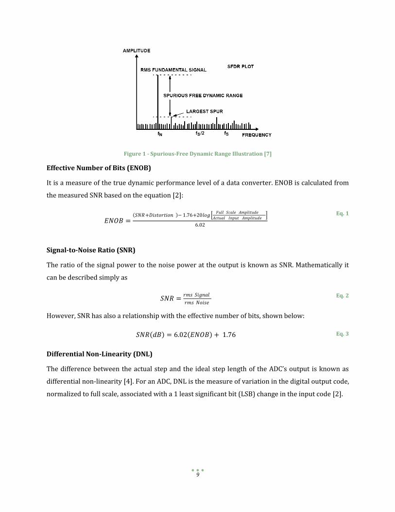
9
Figure 1 - Spurious-Free Dynamic Range Illustration [7]
Effective Number of Bits (ENOB)
It is a measure of the true dynamic performance level of a data converter. ENOB is calculated from
the measured SNR based on the equation [2]:
𝐸𝑁𝑂𝐵 = 𝑆𝑁𝑅+𝐷𝑖𝑠𝑡𝑜𝑟𝑡𝑖𝑜𝑛 − 1.76+20𝑙𝑜𝑔
𝐹𝑢𝑙𝑙 𝑆𝑐𝑎𝑙𝑒 𝐴𝑚𝑝𝑙𝑖𝑡𝑢𝑑𝑒
𝐴𝑐𝑡𝑢𝑎𝑙 𝐼𝑛𝑝𝑢𝑡 𝐴𝑚𝑝𝑙𝑖𝑡𝑢𝑑𝑒
6.02
Eq. 1
Signal-to-Noise Ratio (SNR)
The ratio of the signal power to the noise power at the output is known as SNR. Mathematically it
can be described simply as
𝑆𝑁𝑅 =𝑟𝑚𝑠 𝑆𝑖𝑔𝑛𝑎𝑙
𝑟𝑚𝑠 𝑁𝑜𝑖𝑠𝑒 Eq. 2
However, SNR has also a relationship with the effective number of bits, shown below:
𝑆𝑁𝑅 𝑑𝐵 = 6.02 𝐸𝑁𝑂𝐵 + 1.76 Eq. 3
Differential Non-Linearity (DNL)
The difference between the actual step and the ideal step length of the ADC’s output is known as
differential non-linearity [4]. For an ADC, DNL is the measure of variation in the digital output code,
normalized to full scale, associated with a 1 least significant bit (LSB) change in the input code [2].

10
Figure 2 - Ideal (left) and Non-Ideal (right) Examples of ADC Transfer Function [4]
A change resulting in an error greater than 1 LSB results in lost bits.
Integral Non-Linearity (INL)
Differently from DNL, the integral non-linearity relates to the maximum difference between the
converter’s output from its ideal value. The ideal value can be described as a theoretical straight
line drawn from minus full scale to positive full scale [2]. The figure below shows a graphical
representation of this concept:
Figure 3 - Integral Non-Linearity Example [4]

11
Quantization Error
When a conversion is made, the number is quantized to a finite number of discrete values. The
error associated with this process is known as quantization error.
(a)
(b)
Figure 4 – (a) Quantization Process [8] and (b) Quantization Error Illustrations (right) [4]
As Figure 4 shows, an analog input is quantized to a digital value. However, as Figure 4 indicates,
there is always a margin where the input value falls between two quantization levels, giving the
ADC its quantization error. Improving this margin correlates to increasing the ADCs resolution.
Total Harmonic Distortion
The concept of total harmonic distortion (THD) applies mostly to nonlinear systems where the
power is present in the fundamental frequency as well as its harmonics. This presence of power in
other frequencies contributes to THD. In general, total harmonic distortion is defined as the ratio of
all harmonics generated to the original signal frequency [5]. Mathematically it is mainly expressed
in units of dB by the following relationship [9],
𝑇𝐻𝐷 = 10𝑙𝑜𝑔 𝑉2
2 + 𝑉32 + 𝑉4
2 + ⋯
𝑉𝑓2
Eq. 4
where Vhn is the voltage corresponding to the n-th harmonic of the signal and Vf is the fundamental’s
voltage.
THD can also be represented as a percentage,
𝑇𝐻𝐷 = 𝑉2
2 + 𝑉32 + 𝑉4
2 + ⋯
𝑉𝑓 × 100 Eq. 5

12
Total harmonic distortion is especially important in ADCs when building the input and sampling
blocks, as this report will further detail in its design section.
2.3 OVERSAMPLING CONVERTERS As mentioned in Section 2.1, one of the major types of converters is the oversampling ADC, which
exists in many variations. Oversampling ADCs are characterized as such due to having their
sampling frequency being greater than twice the bandwidth of the signal, i.e.
𝑓𝑛 > 2 ∙ 𝐵𝑎𝑛𝑑𝑤𝑖𝑑𝑡𝑠𝑖𝑔𝑛𝑎𝑙 . These types of circuits are implemented when attempting to obtain
very high accuracy. This is possible because complex and precise analog circuitry is substituted by
the oversampling ADC’s use of digital signal processing techniques. The sacrifice that is made in this
case is the throughput that can be achieved [3].
Figure 5 - Block Diagrams for Nyquist and Oversampled ADCs
One of the advantages of oversampled ADCs is that aliasing is much less of a concern, in comparison
with Nyquist ADCs [3]. That is because the signal’s frequency spectrum has frequencies much more
widely spaced, since the sampling rate is much greater than the signal’s bandwidth. A disadvantage
of oversampling converters is that a large amount of samples are require to perform a conversion
to a desired accuracy, versus the Nyquist ADCs, in which every conversion yields an individual
result.
Oversampled ADCs are a good option for converters where the signal is band limited, like music
systems, etc. Since this project does not deal with an oversampling converter, we will not delve into
more detail concerning oversampling converters.

13
2.4 NYQUIST CONVERTERS A Nyquist ADC is a type of ADC that samples the input signal at twice the bandwidth. This is the
sampling rate adequate for recovering the original signal according to the Nyquist theorem,
i.e. 𝑓𝑛 = 2 ∙ 𝐵𝑎𝑛𝑑𝑤𝑖𝑑𝑡𝐴𝐷𝐶 , where fn is the sampling frequency of the converter. There are several
types of Nyquist ADCs in the analog design world. Johns and Martin [9] compares the present ADC
types with their common uses in terms of speed and accuracy, shown below:
Table 2 - Speed and Accuracy Correlation with ADCs
Low-to-Medium Speed, High Accuracy
Medium Speed, Medium Accuracy
High Speed, Low-to-Medium Accuracy
Integrating Successive Approximation Flash
Two-Step Interpolating
Oversampling Cyclic Folding
Pipelined Time-Interleaved
In the background portion of this paper, we will overview three types of converters that have been
recently used in the NECAMSID Lab: Pipelined, Successive Approximation, and Cyclic.
2.4.1 PIPELINED ADCS A common ADC structure, the pipeline converter receives its name from its multistage nature.
Figure 6 - Block Diagram of a 16-bit Pipelined ADC [8]
As Figure 8 shows, the analog input voltage VIN is sampled and enters the ADC. Each stage of the
converter is responsible for the quantization of a range of bits. Once a stage is completed, its output
residue voltage of becomes the next block’s input. A final block, containing an n-bit ADC resolves
the less significant bits of the converter. Finally a digital block receives each block’s output and
corrects for time and errors. The final decision is then composed.

14
2.4.2 SUCCESSIVE APPROXIMATION ADCS Successive-approximation ADCs are one of the most popular techniques for analog-to-digital
conversion since they are fairly quick in terms of conversion time, while having moderate circuit
complexity. There are several configurations that would qualify as successive-approximation
converters. For brevity of this report, we will elaborate on main successive-approximation concept
and a few variations. For more complete descriptions of different types of successive-
approximation ADCs refer to [9].
Some authors recommend that the reader compare the functionality of a basic successive-
approximation converter as a “binary search” algorithm [9]. An interesting way to think about this
algorithm is to imagine a book with 256 pages, in which you have to guess the page number
containing a specific event in the novel. However, you are only allowed to ask “yes/no” questions.
Therefore, using the binary search algorithm, one would try to approximate the number by first
asking the owner of the book if the event occurs on a page number greater than 128. If the answer
is no, then the next question would then address if the event occurs on a page number greater than
64. If so, then the remaining page range would then be divided by two and the same process would
be repeated. A flow chart presented by [10] is shown below:
Figure 7 - Flow Chart of Successive-Approximation Approach

15
The successive-approximation approach is similar to the anecdote above. The ADC works by
successively determining the bits of the output starting from the most significant bit (MSB) and
then checking the next bits. However, this method is very primitive for the world class types of
ADCs found today. Therefore, many improvements to that concept have been added, such as a
digital-to-analog converter (DAC) based approximation, using a block known as the Successive-
Approximation Register (SAR). A simple diagram of this functionality is shown below:
Figure 8 - DAC-based Successive-Approximation Converter [9]
In this case, a sample-and-hold block is usually needed so that the value being converted remains
constant through the conversion. The SAR is entirely digital and the DAC’s specifications will mostly
determine the speed and accuracy of the converter.
2.4.2.1 Charge Redistribution ADC
Shown in figure Figure 9 is an example of a charge-redistribution ADC [9]. In this case, an array of
capacitors is used. Its advantage is that the sample and hold, DAC, and comparator blocks are all
combined into one block. The following chart explains the operation of Figure 9:
Table 3 - Charge-Redistribution (Figure 9) ADC Explanation
Operation Mode
Description
Sample All but the largest capacitor are charged to input voltage Vin while
comparator is being reset. The largest capacitor is set to Vref/2
Hold Comparator is taken off reset mode. Capacitors are switched to ground, with the exception of largest capacitor,
causing voltage on negative terminal of comparator Vx to become –Vin/2.
Bit Cycling If Vin is negative, the largest capacitor is switched to ground. If Vin is positive, the largest capacitor is remains at Vref/2.

16
Johns and Martin [9] catalogue other more complex types of SAR ADCs, which include calibration
and error correction blocks.
Figure 9 – 5-bit Charge-Redistribution ADC [9]

17
2.4.3 THE CYCLIC ADC A Cyclic converter, also known as an Algorithmic converter, is similar in operation to the successive
approximation converter. However, in the case of the Cyclic ADC, the reference voltage is not
altered. Instead, the error (or residue) of the amplifier is doubled [9].
Figure 10 – High Level Block Diagram of a Cyclic Converter [11]
As the block diagram above outlines, the operation of the cyclic converter functions in the following
manner: First, the input voltage is sampled by the sample-and-hold block. That value is then
compared to a threshold voltage, upon which a digital decision is made, determining a bit value in
the final sequence of the number sampled. A reference voltage is generated by a 1-bit digital-to-
analog converter which is dictated by the digital decision previously made. At the same time, the
input value is amplified by a factor two (ideally). The amplified value is then summed to a reference
voltage +/- VREF, leaving a residue voltage. The residue voltage then becomes the input of the
residue amplifier. This cycle is repeated enough times required to achieve the desired resolution,
earning the device its name. The sequence of decisions corresponds to the output value of the ADC.
2.4.3.1 Understanding the Residue Amplifier
A major part of the cyclic ADC is the residue amplifier. Therefore, in order to better comprehend the
operation of the ADC, we can take a mathematical approach to explain this concept [11]. The
equation below shows the relationship between the residue amplifier’s input and output:
𝑣𝑟𝑒𝑠𝑜𝑢𝑡= 𝐺 ∙ 𝑣𝑟𝑒𝑠 𝑖𝑛
− 𝑑 ∙ 𝑉𝑟𝑒𝑓 Eq. 6
where G is the gain of the amplifier and d is the digital decision.

18
Assuming ideal conditions, after performing N cycles, the amplifier exhibits the following negative
feedback loop relationship:
𝑣𝑟𝑒𝑠𝑜𝑢𝑡 (𝑁) = 𝐺𝑁 ∙ 𝑣𝑟𝑒𝑠 𝑖𝑛 − 𝐺𝑁−1𝑑1 + 𝐺𝑁−2𝑑2 + ⋯ + 𝐺0𝑑𝑁 ∙ 𝑉𝑟𝑒𝑓 Eq. 7
We can also predict the output code of the ADC by rearranging Eq. 7 into the following form [11]:
𝑣𝑟𝑒𝑠 𝑖𝑛
𝑉𝑟𝑒𝑓=
1
𝐺𝑑1 +
1
𝐺𝑁−1𝑑2 + ⋯ +
1
𝐺𝑁𝑑𝑁 −
1
𝐺𝑁 𝑣𝑟𝑒𝑠𝑜𝑢𝑡 (𝑁)
𝑉𝑟𝑒𝑓
Eq. 8
We can define the 1
𝐺𝑁 𝑣𝑟𝑒𝑠 𝑜𝑢𝑡 (𝑁)
𝑉𝑟𝑒𝑓 term of the equation as the quantization error, and the first term as
the output code x:
𝑥 = 1
𝐺 𝑑1 +
1
𝐺
2
𝑑2 + ⋯ + 1
𝐺 𝑁
𝑑𝑁 Eq. 9
A plot relating the residue amplifier’s input and output can be created, as shown below:
Figure 11 - Residue Plot at G=2 [11]
Figure 12 - Residue Plot with G < 2 [11]
However, maintaining a constant gain of 2 may be challenging. Therefore, when G < 2, the residue
plot would look like Figure 12. This event makes it possible for two possible decisions for the same
input value, adding redundancy to the ADC. However, at the same time, it adds a level of complexity
to the calibration of the converter, which will be discussed in a further section of the document.

19
2.5 THE ROLE OF CAPACITORS As the previous section has outlined, the used of capacitors for ADCs is very common. In our, as the
design sections of this paper will indicate, relies heavily on the use of multiple capacitors that will
be switched constantly to perform the cyclic function of our ADC. Therefore, we must understand
how they will affect our circuit and what constraints we are faced with when choosing the correct
capacitors for our circuit.
2.5.1 THERMAL NOISE Thermal noise is inherent to all electronic circuits and it is caused by a random motion of electrons
in a conductor. It is a function of temperature and is constant over all frequencies. When designing
an analog to digital converter, this noise must be accounted for in the design of the sampling
capacitors. That way, the sample-and-hold amplifier (SHA) will achieve desirable signal-to-noise
ratios. Since the SNR is the integral of all the noise in a system, the lower the noise bandwidth, the
less noise is sampled by the ADC. Figure 13 below shows a model of a sample and hold switch with
a dc input and a thermal noise.
Hold
Capacitor
+
Vhold
-
Switch Resistance
Thermal
Noise
Sample Switch
DC signal
Figure 13- Diagram of Hold capacitor with Thermal Noise
When the sample switch is opened the voltage on the capacitor is the DC signal and the thermal
noise at the instant the switch is opened. Since the characteristic of the sample and hold circuit is a
low pass filter the noise above the cutoff frequency of the circuit is attenuated. In order to reduce
the bandwidth of the noise the hold capacitor must be sized according to the SNR needed.
The equation below shows the relationship of capacitance and temperature to the RMS noise of a
system, which is the ratio of capacitor size to the total thermal noise power of the RC circuit.
𝑅𝑀𝑆 𝑛𝑜𝑖𝑠𝑒 = 𝐾𝑇
𝐶
Eq. 10

20
2.6 OPTIONS FOR OUTPUT DRIVING Every analog-to-digital converter has to interact with an off-chip digital domain, usually an FPGA.
Although sometimes designers may choose additional output drivers in their circuit at the expense
of simplicity, there are methods used to improve output performance. In this case, various methods
were researched. One particular method, known as Low Voltage Differential Signaling (LVDS),
showed itself to be a promising option for our circuit. Section 2.6 outlines the existing
configurations and applications of LVDS.
2.6.1 UNDERSTANDING LVDS Usually used for output blocks of ADCs, Low-Voltage Differential Signaling is a technology that was
officially introduced in 1994 by National Semiconductor. It was born out of the necessity to create
high performance solutions that consume little power and are susceptible to less noise than the
common techniques of the time, while being cost-effective, such as RS-442 and RS-485 standards. A
competing technology was Emitter Coupled Logic (ECL). However, it is incompatible with standard
logic levels, uses negative power rails, and leads to high chip-power dissipation [12].
Table 4 - Comparison Table of Differential Standards
2.6.2 THE CONCEPTS BEHIND LVDS LVDS, as the name suggests, is differential – meaning that it makes use of two signals to function. At
the cost of using an extra trace and space, noise is considerably reduced through common-mode
rejection. As a consequence, many improvements can be made to the design, such as:
Signal swing can be dropped to only a few hundred millivolts due to signal-to-noise
rejection improvement
Rise time is shorter, resulting in faster data rates
Very low power consumption across a wide range of frequencies due to low swing and
current-mode driver outputs

21
2.6.3 DIFFERENT TYPES OF LVDS The table below shows the different variations of LVDS found in the market today:
Table 5 - Industry Standards for Various LVDS Technologies [13]
While the concept of LVDS is the foundation of the standards found in the table above, there are
various applications for each one. Power consumption, performance, and target application are
among the differences listed above. For brevity, we will analyze the typical LVDS standard and how
it applies to this project. If applicable, the other technologies may be explored.
Different Configurations of LVDS
There are three common Bus types of LVDS configurations. They are:
Point-to-Point
Multidrop
Multipoint
2.6.3.1 Point-to-Point
Being the simplest configuration, Point-to-Point offers a direct path from the transmitter to the
receiver. This is favorable for use in the highest data rates, due to the simple path. A variation of
this configuration can be seen in Figure 15. All figures in this section are extracted from [12].
Figure 14 - Point-to-Point Configuration
Figure 15 - Data Distribution Using Point-to-Point Configuration

22
2.6.3.2 Multidrop
Multidrop is most efficient when various parts of a circuit need to receive the same information.
There is one driver and two or more receivers along the bus, as the figure below illustrates:
Figure 16 - Multidrop Configuration
2.6.3.3 Multipoint
A multipoint configuration uses various drivers and receivers. The advantage to this circuit is that it
can send information from multiple areas of the circuit, if necessary. However, this configuration
can get quite complex and speeds are generally lower than the other simpler configurations.
Figure 17 - Example of a Three-Node Multipoint Configuration
2.6.4 CONTRASTING LVDS TYPES AND CONFIGURATIONS The article released by National Semiconductor entitled “The Many Flavors of LVDS” [12]
summarizes the available technologies with the configurations used by them. This matrix is shown
below:
Table 6 - Bus Configurations vs. Standards

23
2.6.5 A TYPICAL LVDS CIRCUIT The following picture illustrates a high-level configuration for a LVDS circuit. Notice the detail
showing the reduction in interference due to the interaction in electric fields between the wires,
which are usually placed as a twisted pair.
Figure 18 - LVDS Driver and Receiver [13]
In the driver-receiver configuration shown in Figure 18, a 3.5mA current source is found in the
driver. Due to the high impedance “op-amp characteristic” of the receiver, all of the current flows
through the 350mV resistor in place. When the driver makes a switch, the current changes
direction of flow across the resistor and results in a logic state “one” or “zero.” Figure 19 illustrates
this concept.
Figure 19 - Digital Signaling Model

24
2.6.6 APPLICATIONS There are various applications for LVDS. As previously mentioned, the advantages presented by
LVDS make it a popular technology. Listed below are three common applications of LVDS within
integrated circuits.
Line drivers/receivers – Commonly used to convert single-ended signals into formats for
transmission over a cable or backplane.
SerDes – Serializer/deserializer pairs are used to multiplex a number of low-speed CMOS
lines and to transmit them as a single channel running at a higher data rate.
Switches – Used instead of bus architectures for high data rates. Commonly used for clock
distribution. LVDS is one of the most suitable signaling standards for clocks of any
frequency because of reliable signal integrity.
2.6.7 ASSESSING LVDS IN THE ADC DESIGN PROCESS There are various factors to consider when choosing a signaling standard, such as:
Required bandwidth
Ability to drive cables, backplanes, or long traces
Power budget
Network topology (point-to-point, multidrop, multipoint)
Serialized or parallel data transport
Clock or data distribution
Compliance to industry standards
Need or availability of signal conditioning

25
2.7 THE SPLIT-ADC CONCEPT One of the key characteristics of our project is that it is meant to use a Split-ADC architecture. The
figure below illustrates the basic principle of the split-ADC. Instead of using one converter, the chip
will have two ADCs performing the same steps over the same input. The output then becomes the
average of both results. The difference of each ADC’s output is then sent to the error estimation
block, which is located off chip, in the digital realm [14].
Figure 20 - Illustration of Split-ADC Concept [11]
Ideally, the concept behind the split-ADC architecture is simple to comprehend: when the difference
between outputs xA and xB is zero, the calibration has occurred. This concept is important because it
will reduce the circuit’s calibration time significantly, as explained in [11]. The following graph
contrasts the single ADC approach versus a split architecture.
Figure 21 - Split ADC Characteristics in Contrast with Single ADC Approach

26
As Figure 21 shows, the trade off in complexity is small compared to the advantages in calibration.
At the same time, the general speed, power and noise of circuit remains the same. This is because
the same parts are used but in proportions of one half the original size.
2.8 THE CURRENT MIRROR Biasing is very important to our project, making the necessity to build current sources imminent.
One of the most common forms of creating a current source is by using a MOSFET current mirror.
The current mirror relies on the assumption that transistors are closely matched, meaning that they
are fabricated under the same conditions, matching closely the values of the transistors’ threshold
voltages, mobility, and oxide capacitance. Therefore, since this level of matching and precision can
only be achieved in integrated circuits, the current is not commonly realized with discrete
components. Figure 22 shows a basic configuration for a current mirror.
Figure 22 - Current Mirror Example
According to the MOSFET Square Law, we can define the current in the transistors as [3]:
𝐼𝐷 =𝜇𝑛𝐶𝑜𝑥
2
𝑊
𝐿(𝑉𝐺𝑆 − 𝑉𝑡)2 Eq. 11
where ID is the MOSFET drain current, Cox is the capacitance of the oxide, W is the width of the
transistor, L is the length, VGS is the gate to source voltage and Vth is the threshold voltage of the
transistor. Therefore for the current ID1 in transistor M1, we can solve for VGS1,
𝑉𝐺𝑆1 = 2∙𝐼𝐷1 ∙𝐿1
𝜇𝑛𝐶𝑜𝑥 𝑊1+ 𝑉𝑡1 Eq. 12

27
As shown in Figure 22, by tying the MOSFET gates together, we force the following relationship:
𝑉𝐺𝑆1 = 𝑉𝐺𝑆2
We can now input our value for VGS1 into the current of the second transistor:
𝐼𝐷2 =𝜇𝑛2𝐶𝑜𝑥 2
2
𝑊2
𝐿2
2∙𝐼𝐷1 ∙𝐿1
𝜇𝑛𝐶𝑜𝑥 𝑊1+ 𝑉𝑡1 − 𝑉𝑡2
2
Assuming the matching conditions mentioned above, we can assume that
𝜇𝑛1 = 𝜇𝑛2
𝐶𝑜𝑥1 = 𝐶𝑜𝑥2
𝑉𝑡1 = 𝑉𝑡2
Simplifying our results to
𝐼𝐷2 = 𝐼𝐷1 𝑊2𝐿2
𝑊1𝐿1
Eq. 13
When comparing the current mirror to an ideal current source, the model falls short in a few
aspects. For example, an ideal source has infinite AC impedance, while a MOS mirror has finite
impedance. Also, the current mirror will have frequency limitations due to capacitive parasitics.
2.9 THE DIFFERENTIAL PAIR The differential pair, sometimes referred to as the differential amplifier, is a vital part of our circuit.
According to Sedra and Smith, “the differential pair is the most widely used building block in analog
integrated-circuit design.” This is because differential amplifiers are less susceptible to noise than
their single-ended counterparts and they also allow for biasing of an amplifier without the use of
bypass and/or coupling capacitors, saving space on the chip being manufactured [15]. As with the
current mirror, in integrated circuits, the differential pair relies largely on the ability to match
components.
The differential pair can be used in various configurations. In this section we will explore two
modes of operations: common-mode and differential gain modes. An example of a differential pair
is shown below:

28
Figure 23 - Differential Amplifier Example [16]
The differential pair consists of a symmetrical system of two MOSFETS sharing the same bias
current. The parameters in each transistor can be extracted using the square law equation, seen in
Eq. 11:
𝐼𝐷 =𝜇𝑛𝐶𝑜𝑥
2
𝑊
𝐿(𝑉𝐺𝑆 − 𝑉𝑡)2
where the currents at each transistor are equal to 𝐼𝐷
2.
2.9.1 BARTLETT’S BISECTION THEOREM The functionality of the system can be explored using Bartlett’s Bisection Theorem, which is based
on the symmetry of circuits and explores the fact that any two inputs can be represented in a
common mode and a differential mode.
Figure 24 –Amplifier Model
Figure 25 - Common Mode Model
Figure 26 - Differential Mode Model

29
The common-mode voltage can be defined as:
𝑉𝑐 =𝑉1+𝑉2
2 Eq. 14
And the differential voltage as:
𝑉𝑑 = 𝑉2 − 𝑉1 Eq. 15
Using this concept, we can also verify that:
𝑉1 = 𝑉𝑐 −𝑉𝑑
2 Eq. 16
and
𝑉2 = 𝑉𝑐 +𝑉𝑑
2 Eq. 17
We can represent the half circuit of each circuit model for the example in Figure 23 using the
bisection theorem, as shown below:
Figure 27 - Half-Circuit Model of the Common Mode
Figure 28 - Half-Circuit Model of the Differential Mode

30
A graph of the large signal characteristics of the differential pair is shown below:
Figure 29 - Signal Input-Output Characteristics of the Differential Input to Each Output
Figure 30 - Large Signal Input-Output Characteristic for the Differential Input to the Differential Output
To simplify calculations and circuitry it is common practice to attempt to operate with the linear
areas of the curves shown above. As we said in the introduction, one of our project’s major steps is
that non-linearity is not as much of a pertinent issue to our circuit, as we will see in later sections.

31
3 HIGH-LEVEL DESIGN
The objective of this section is to give a brief high level overview of the integrated circuit being
designed for this project.
3.1 BLOCK DIAGRAM The figure below displays a proposed block diagram for the device. Several sub blocks are displayed
in the diagram. This approach gives us a modular idea of the design.
They main blocks found in our design are:
Switch Capacitor Array
Open Loop Differential Amplifier
Bias Circuitry
Comparator Network
Logic Sub Block
Output Drivers
Figure 31 - Block Diagram

32
3.2 THE I/O PIN LIST ***REDO THIS SECTION AFTER TALKING ABOUT PINS AGAIN!***
Figure 32 - I/O Pin Diagram
The block diagram is a starting point toward the more complex steps of the design. As mentioned
above, the block diagram can be used as an analytical tool for simplifying the design steps. Besides
the block diagram the I/O pin diagram is featured is this report. The I/O pin diagram is designed
with several assumptions in mind and due to such conditions it is a subject to changes as needed in
future.

33
4 THE INPUT BLOCK
The input of our ADC is composed of a sample-and-hold circuit that will enable us to obtain the
analog input into the input capacitors. Our input block can appear quite complex at first, since we
are using multiple capacitors. Therefore, for simplicity and visualization of concept, we will first
start with a basic concept for the input block, shown below:
Figure 33 - Schematic of Input Block
As the figure above shows, in this simplified version of the input block, the input voltage Vin is
sampled onto capacitor C1. It is done so through a CMOS transmission gate, a configuration
involving a pair of opposite type MOSFETs. The use of transmission gates eliminates the
undesirable threshold voltage effects which give rise to loss of logic levels [3]. The capacitor is
sampled at every positive of edge of the clock cycle, indicated in this case as Vclkp, and at every
negative edge of its inverted version, Vclkm, to bias the p-channel transistor.1
1 Note: Biasing for transistor M3 is simplified. In actual implementation, the gate voltage on M3 in Figure 33 is
delayed slightly to reduce charge injection.

34
4.1 TRANSISTOR SIZE OPTIMIZATION Transistors in this block need to be properly sized to accommodate our circuit. This task is more
important than it seems. The transistor sizes will help determine and/or improve several factors of
the ADC, such as spurious-free dynamic range and total harmonic distortion. Therefore, an
optimization exercise was necessary to determine the correct widths of the transistors which
would meet our goals for distortion and acquisition time.
4.1.1 DEALING WITH THE PRESENCE OF DISTORTION One might wonder why distortion is such an important issue to such a simple circuit, like our input
block. The key is that distortion is present due to variations on the gate voltage. We’ll start by
looking at the equation for the “on” resistance of the MOSFET:
𝑅𝐷𝑆𝑜𝑛=
𝑉𝐷𝑆
𝐼𝐷=
1
𝜇𝑛𝐶𝑜𝑥𝑊
𝐿 𝑉𝐺𝑆 −𝑉𝑇𝐻
Eq. 18
All of the values in Eq. 18 are mostly constant, with the exception of the voltage from gate to source,
which will constantly with the sampling nature of the input. This change in VGS causes the internal
resistance of the transistors to change as well. Since the transistor sizes will be different, the values
in RDSon will not change uniformly. All of these factors contribute to distortion of the signal.
4.1.2 PERFORMING A PARAMETRIC ANALYSIS Our goal for this analysis was to determine the input block’s transistor widths. From previous
design experience, professor McNeill recommended the following assumptions:
The p-channel (M2) transistor will have a width that is 4 times larger than its n-channel
MOSFET equivalent
The n-channel MOSFET (M3) on the top plate of the capacitors should have a width
proportional (by a factor of x), but not necessarily equal, to the n-channel MOSFETs (M1) on
the bottom plate
We can look at this issue as a matter of how much total transistor width we can afford in the chip, in
terms of chip area. Therefore, we can determine the total width, WTotal, as a function of M1’s width,
as shown below:
𝑊𝑇𝑜𝑡𝑎𝑙 = 𝑊𝑄1+ 𝑊𝑄2
+ 𝑊𝑄3= 𝑊 + 4𝑊 + 𝑥𝑊 Eq. 19
Rearranging,
𝑊𝑇𝑜𝑡𝑎𝑙 = 5 + 𝑥 ∙ 𝑊
𝑊 =𝑊𝑇𝑜𝑡𝑎𝑙
5+𝑥 Eq. 20

35
As a result, we created a series of graphs, where the values for x, W, and WTotal were swept, to find
the smallest transistors that would fit our needs. The two main characteristics that relate to these
values are acquisition time and total harmonic distortion. To deliver values for those attributes, we
had to run several parametric equations on Cadence. The following table indicates the values that
were simulated:
Table 7 - Swept Attributes
x 0.1 0.2 0.5 1 2 5 10
WTotal 10µm 20µm 50µm 100µm 200µm 500µm 1mm 2mm 5mm 10mm
The title of each graph indicates the values used for WTotal. On the y-axis, the red lines indicate THD
and the blue lines indicate acquisition time. The x-axis indicates the value of x.
Note: The values of x are scaled by a factor of 20, in order to accommodate simulation criteria in Cadence.

36

37
The results are summarized in the table below:
Table 8 - Summarized Optimization Results of tACQ and THD
WTotal
[µm] x tACQ
[ns] THD [%]
10 0.25 85 1.8 20 0.5 50 1.0 50 0.5 30 0.6
100 0.5 12 0.3 200 0.5 6 0.15 500 0.5 3 0.06
1000 0.5 1.9 0.035 2000 0.5 1.5 0.025 5000 0.5 1.1 0.016
10000 0.5 1.09 0.012
The values chosen were dictated by minimum of THD, which happened at the lower side of
acquisition time curve. We can observe that there is a relationship between the total width of the
transistors and the parameters simulated. This relationship is shown below in Figure 34 and Figure
35.
Figure 34 - THD and WTotal Relationship
Figure 35 - Acquisition Time and WTotal Relationship
As the figures above indicate, the larger widths will give us better parameters. However, the sizes
used for testing are rather large and must be taken into account, meaning that a compromise will be
made. As a result, our next step was to set goals for distortion and acquisition time that will
establish the basis for this compromise.

38
4.1.2.1 Goals for Parameters
To ensure that our design is competitive, Professor McNeill has indicated that from experience, the
level of total harmonic distortion should be less than 0.01%. Once again, the Professor’s experience
in analog integrated circuit design served as a guide for an acquisition time goal. As defined in the
introduction of the paper, the ADC will perform one million samples per second, translating into 1
conversion per microsecond. Therefore, we have decided to allow twenty percent of this time for
sampling the input. The reason for this will be discussed later. Therefore, the goals for our ADC
input parameters are as follows:
Table 9 - Parameter Goals
Parameter Goal
Total Harmonic Distortion < 0.01%
Acquisition Time < 200 ns
As the graphs show, the acquisition time is not an issue for us, since all measurements met the
required goal. The reason for such a loose acquisition time goal will be explained in a further
subsection.
4.1.3 CHOOSING TOTAL WIDTH When looking at our simulation results, we can see that the total harmonic distortion levels found
were not below the expected mark of 0.01%. The reason for this is inferred to be the limitations of
the simulator. The simulations were done under various conditions and yielded different results.
However, when looking at Cadence’s description of the THD formula, some parameters were not
easily editable. As a result, we assumed that the total harmonic distortion levels are low enough at
high values for total width that we were at a very safe margin at a WTotal value of 5mm.
As stated in Eq. 20, the equation derived that gives us our parameters for width is:
𝑊 =𝑊𝑇𝑜𝑡𝑎𝑙
5+𝑥
Since we have established through the analysis that the total width is 5mm, we can plug in the
respective values from Table 9.
𝑊 =5𝑚𝑚
5+0.5
𝑊 = 909µ𝑚

39
Summarizing our new transistor widths:
Table 10 - Values for Transistor Widths
M1 M2 M3
Expression W 4W xW
Value 909 µm 3.63 mm 454.5 µm
4.2 REDUCING THE NOISE FLOOR Until this point in the design of the input block, acquisition time has been a specification easily met.
However, the reason for which we allotted 200ns for the ADC to sample is related to spectral noise
reduction and SNR. In order words, the internal “on” resistance of the MOSFETs, combined with the
input capacitor, create a frequency roll-off at a high frequency. The picture below shows an example
of this case.
Figure 36 – Motivation for Noise Floor Reduction
If rDSon takes on a value of 50 Ω, the frequency roll off, fh, will be found at 8 MHz, or in theory,
𝑓 =1
2𝜋∙𝑅𝐶 Eq. 21
The blue shading indicates the location of the frequency roll-off. However, since our ADC’s
bandwidth is simply 500 kHz, we can decrease the length of the noise floor by adding a resistance
to the circuit, as shown in Figure 37.

40
Figure 37 - New Input Circuit Model with Added Resistor
To find this resistance, we must find how many time constants are necessary to obtain the precision
desired for the ADC. In this converter, since we are attempting to have a 16-bit converter, the
accuracy level is going to be within ½ Least Significant Bits of the ADC, as shown below:
𝑡𝑎𝑙𝑙𝑜𝑤 = ln 217 ∙ 𝜏 Eq. 22
where τ is the RC circuit’s time constant and tallow is the value pre-determined as the input sampling
duration. Restructuring the equation, we’ll have:
𝜏 =𝑡𝑎𝑙𝑙𝑜𝑤
ln 217 ≈
200 𝑛𝑠
12= 16 𝑛𝑠
Knowing that our 𝜏 = 𝑅𝐶 time constant is 16ns, we can solve for the resistor size. Since we have
a capacitor value of 4pF on C1,
𝑅 =16 𝑛𝑠𝑒𝑐
4𝑝𝐹
𝑅 = 4𝑘𝛺
As expected, the input block will now have its acquisition time increased drastically. However, we
had already allotted 200ns for the sampling of the circuit. To ensure the acquisition time is under
200ns, the figure below shows the acquisition time according to the different resistance values from
0 to 10kΩ:

41
Figure 38 - Acquisition Time Dependence after Adding New Resistor
4.2.1 RESISTOR TOLERANCE According to the JAZZ library help files, the resistor tolerances will vary approximately by 25%.
That assumption is made based on the following documentation:
Therefore, we can see that our circuit may have a higher acquisition time than expected at 5kΩ.
However, that time is still below the 200ns mark.
Table 11 – Effect of Tolerances
-25% Expected +25%
Value 3 kΩ 4 kΩ 5 kΩ tACQ 111 nsec 148 nsec 185 nsec
To see the variation, the THD was also simulated. We can see that the swing in distortion does not
vary much, as shown in Figure 39.

42
Figure 39 - THD Dependence on Resistor Variation
Using Eq. 21, our roll-off frequency will now be
𝑓 =1
2𝜋∙𝑅𝐶=
1
2𝜋∙16𝑛𝑠= 9.95 𝑀𝐻𝑧
𝑓 ≈ 10 𝑀𝐻𝑧
As stated in Section 2.5.1, the SNR of ADC is the integral of all the noise in a system. Therefore, by
reducing the noise floor, we have reduced the signal-to-noise ration of the ADC as well.
4.2.2 IMPLEMENTATION OF INPUT BLOCK In the actual input block, we will use 4 capacitors in of size 1pF. Therefore we have to size all
transistors accordingly. The next page shows a diagram of this concept. Also, a Split-ADC
architecture will be used, meaning that the capacitor values will be half of the current values.
Instead of four capacitors, eight will be used and the resistor will be sized appropriately.

43
Vclkp
Vclkm
C1A
Vicm
Vinp
Vdd
N-MOS
P-MOS
N-MOS
Vclkp
WL
0.25WL
xWL
C1B
C1C
C1D
Rin1
C2A
C2B
C2C
C2D
Vicm
Vclkp
Rin2
Vinm
N-MOS xWL
Vclkp
Vclkm
Vdd
N-MOS
P-MOSWL
0.25WL
Vclkp
Vclkm
Vdd
N-MOS
P-MOSWL
0.25WL
Vclkp
Vclkm
Vdd
N-MOS
P-MOSWL
0.25WL
Vclkp
Vclkm
Vdd
N-MOS
P-MOSWL
0.25WL
Vclkp
Vclkm
Vdd
N-MOS
P-MOSWL
0.25WL
Vclkp
Vclkm
Vdd
N-MOS
P-MOSWL
0.25WL
Vclkp
Vclkm
Vdd
N-MOS
P-MOSWL
0.25WL
44
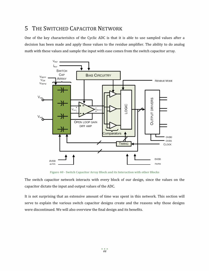
5 THE SWITCHED CAPACITOR NETWORK
One of the key characterisitcs of the Cyclic ADC is that it is able to use sampled values after a
decision has been made and apply those values to the residue amplifier. The ability to do analog
math with these values and sample the input with ease comes from the switch capacitor array.
Figure 40 - Switch Capacitor Array Block and its Interaction with other Blocks
The switch capacitor network interacts with every block of our design, since the values on the
capacitor dictate the input and output values of the ADC.
It is not surprising that an extensive amount of time was spent in this network. This section will
serve to explain the various switch capacitor designs create and the reasons why those designs
were discontinued. We will also overview the final design and its benefits.

45
5.1 DEFINING THE CORRECT NUMBER OF CAPACITORS FOR THE NETWORK An important of our design, which adds to its level of complexity, is the number of capacitors used
in the network. More capacitors equate to more transistors being used for switching and
transmission. Therefore, our approach is to be conservative in the number of capacitors used.
5.1.1 USING ONE CAPACITOR Before we describe our approach it is important to define what is meant by using one capacitor. As
the simplified diagram below shows, there is one capacitor on the input and one capacitor on the
output of the differential amplifier. The differential counterpart is not considered in this example
for simplicity. One capacitor means that the amplifier’s input will have one capacitor and the
amplifier’s output will have one capacitor as well. This number is doubled for the differential
functionality.
Figure 41 - Example of Using One Capacitor
Although the approach of using one capacitor makes the circuit’s functionality very simple, this
approach proved to be ineffective immediately. This is due to a simple factor. Symbolized in the
graph as VDAC is the block responsible for choosing a decision based on a previous block. The
decision created by this block results in the switching to its respective voltage reference. However,
since our differential amplifier does not have a perfect gain of 2, two additional decisions need to be
made. With this design, two additional voltage references would need to be created. Since industry
standards and common practice usually limit the amount of off-chip reference voltages, we felt it
was necessary to introduce an extra capacitor to incorporate decisions -2, -1, 0, +1, and +2.

46
5.1.2 USING TWO CAPACITORS To incorporate the desired decisions, the use of 2 capacitors was then implemented. Since we have
a positive, negative, and common mode reference voltage available for each capacitor, the resulting
decision would be represented as the diagram below indicates:
Figure 42 - Diagram of Decisions with 2 Capacitors
As Figure 42 indicates, the sum of the value on the top plates of the capacitors will be the input of
the differential amplifier. This approach makes it possible to introduce the desired +/- 1 decisions.
In comparison with Figure 41, the value of each capacitor in this new design is half the size of the
single capacitor configuration, making the total capacitance the same.
5.1.3 TESTING THE TWO CAPACITOR SYSTEM As our testing indicated, implementing the +/- 1 decisions was now possible, but not as effective as
expected. The circuit used for testing this decision is shown below:
Figure 43 - Test Circuit for +/- 1 Decision

47
In other decisions, no charge is redistributed into the capacitors before switching. However, in this
case, the issue lies with the fact that the +/- 1 decision mode does give the two capacitors a
difference in potential, meaning that the capacitors will redistribute their charge when attached to
the same node. Also, for our differential amplifier to obtain the predertimend desired settling time
of 1 nanosecond or less, the MOSFET widths had to be made very large. As result, the parasitics on
the gates of the transistors cause a tremendous amount of charge injection into the capacitors. The
figure belows shows this occurance:
Figure 44- Example of Charge Injection: Capacitor being Switched between a 500µm PMOS and a 250µm NMOS
As the transient response above shows, over 100mV of impact is done by charge injection, indicated
by point M1. Therefore a new alternative had to be created.
5.2 THE FINAL SWITCH CAPACITOR DESIGN: FOUR CAPACITORS Our approach in resolving this issue was to try to minimize the charge injection coming from the
gate of the transistors. This effect is due to a high internal resistance of the transistor, caused by
low overdrive voltages. The low overdrive voltage was mainly found in the transistors that switch
to Vicm. Consequently, an alternative was to not use Vicm as a reference voltage. Instead, some analog
math would be done with four capacitors to give the same voltage levels desired in the previous
iterations of the design. Therefore, by increasing the number of capacitors, we can decrease the
overdrive voltage on the MOSFETs and have less charge injection. We used a total of 4 capacitors,
each with a value of ¼ of the original.

48
The following figure shows the new manner in which the decisions are made:
Figure 45 - Method for Using 4 Capacitors
Figure 46 shows the simulated circuit for the 4 capacitor approach:
Figure 46 - Circuit Implemented with 4 Capacitors

49
Using the 4 capacitor implementation, the overdrive voltages for the MOSFETS are much greater,
reducing the Rdson of the MOSFETs allowing much smaller widths to be used. Using this
implementation charge injection is reduced by a factor of about 4. The figure below shows a
comparison of the 2 capacitor model and the 4 capacitor model for the implementation of the +1
decision.
Figure 47- Comparison of 2 and 4 Capacitor Implementation of +1 Decision
As seen in the figure above, using the four capacitor circuit for the implementation of the +1
decision reduces the input settling time to around 340ps while reducing the charge injection to
38mV. As seen in the figure below, this improvement is seen across various capacitor voltages.
Figure 48 Comparison of 2 and 4 Capacitor Implementation of +1 Decision
50
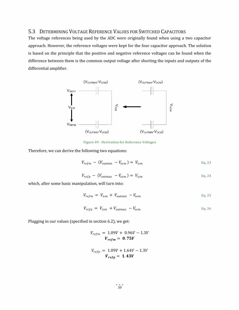
5.3 DETERMINING VOLTAGE REFERENCE VALUES FOR SWITCHED CAPACITORS The voltage references being used by the ADC were originally found when using a two capacitor
approach. However, the reference voltages were kept for the four capacitor approach. The solution
is based on the principle that the positive and negative reference voltages can be found when the
difference between them is the common output voltage after shorting the inputs and outputs of the
differential amplifier.
Figure 49 - Derivation for Reference Voltages
Therefore, we can derive the following two equations:
𝑉𝑟𝑒𝑓𝑚 − 𝑉𝑜𝑢𝑡𝑚𝑖𝑛 − 𝑉𝑜𝑐𝑚 = 𝑉𝑖𝑐𝑚 Eq. 23
𝑉𝑟𝑒𝑓𝑝 − 𝑉𝑜𝑢𝑡𝑚𝑎𝑥 − 𝑉𝑜𝑐𝑚 = 𝑉𝑖𝑐𝑚 Eq. 24
which, after some basic manipulation, will turn into:
𝑉𝑟𝑒𝑓𝑚 = 𝑉𝑖𝑐𝑚 + 𝑉𝑜𝑢𝑡𝑚𝑖𝑛 − 𝑉𝑜𝑐𝑚 Eq. 25
𝑉𝑟𝑒𝑓𝑝 = 𝑉𝑖𝑐𝑚 + 𝑉𝑜𝑢𝑡𝑚𝑎𝑥 − 𝑉𝑜𝑐𝑚 Eq. 26
Plugging in our values (specified in section 6.2), we get:
𝑉𝑟𝑒𝑓𝑚 = 1.09𝑉 + 0.96𝑉 − 1.3𝑉
𝑽𝒓𝒆𝒇𝒎 = 𝟎. 𝟕𝟓𝑽
𝑉𝑟𝑒𝑓𝑝 = 1.09𝑉 + 1.64𝑉 − 1.3𝑉
𝑽𝒓𝒆𝒇𝒑 = 𝟏. 𝟒𝟑𝑽

51
6 DIFFERENTIAL AMPLIFIER
The following section concerns the differential amplifier block. Shown below is the schematic
representation of the differential amplifier and supportive components attached to it. The behavior
of the differential amplifier and equations that governed its qualitative analysis were introduced
previously in section 2.9. The role of each supportive component will be described in separate
sections that follow. The goal regarding the design of the differential amplifier was using an open-
loop differential amplifier in order to reduce the power consumption. The nonlinearity introduced
by the open-loop configuration was planned to be processed by digital means.
Shown below is the differential amplifier circuit in transistor level. Components that form the
whole circuits will be described below. In order to gets a better understanding regarding the role of
each transistor in this circuit; it would be helpful to group together the ones that interact with each
other.
VDD
I_in (input current to bias
the block)
RD RD
VDDVDD
Out1 Out2
Gnd
Reset_Out
Vocm
Reset_Out
Vocm
In1 In2
Reset_In Reset_In
Vicm Vicm
VDD
M3rep M4rep
M1 M2
M5
M6 M7
M8M9
M10
M11M12
Figure 50-Schematic Representation of Differential Amplifier

52
6.1 FUNDAMENTAL COMPONENTS OF THE DIFFERENTIAL AMPLIFIER Indentifying transistors that form parts of the differential amplifier are listed below. By doing so,
one can simplify the analysis of a complicated circuit such as the circuit in discussion.
The main part of this circuit is the differential amplifier that is composed by M1, M2, M9,
and both RD resistors.
Replica bias sub circuit is composed by M3rep, M4rep, M5, and M11.
The transistor, M10, sets the gate voltage for M9 and M11.
Transistors M6 and M7 allow for resetting the output of the differential amplifier to a
known value of the output common mode.
Transistors M8 and M12 also allow for resetting the input of the differential amplifier to
input common mode value.
6.2 DIFFERENTIAL AMPLIFIER VOLTAGE LEVELS Another aspect of the differential pair design was choosing the input, output, and common mode
voltage levels for the device. In order to start the design for this part known variables were listed
and several assumptions were initially considered.
Power supply rails range from ground (VSS = 0V) to VDD = 1.8V.
Threshold voltage for the transistors used in designing the differential amplifier was
selected, Vth = 0.45V. The threshold voltage was found in the available Jazz libraries.
Figure 51- Differential In-Out Characteristic

53
The derivation of the voltage levels started based on four equations, which will be discussed in this
section. The first set of equations involves determining the triode crashes within the differential
amplifier. The derivation of the following equations were based on the limitations that differential
amplifier faces. Below is shown the input output characteristic graph for the differential amplifier
which served as a guide to derive the equations that govern the input and output ranges of the
differential pair.
The low triode crash happens when inputs are equal to each other. In other words:
𝐿𝑜𝑤 𝑡𝑟𝑖𝑜𝑑𝑒 𝑐𝑟𝑎𝑠 → 𝑉𝐼𝑃 = 𝑉𝐼𝑀 = 𝑉𝐼𝐶𝑀 Eq. 27
An assumption made regarding the transistor, M9, that serves as the biasing of the differential
amplifier was that the minimum drain to source voltage must be equal to, VDS = 0.3V for this device
to be in saturation region.
Below are shown known voltages and the equation for the gate to source voltage for M1.
Vth = 0.45V
VDS = 0.3V
𝑉𝐺𝑆1 = 𝑉𝑡 + 𝑉𝑜𝑣1 Eq. 28
The four base equations used were the following;
Eq. 29 describes the low triode crash of the device:
𝑉𝐼𝐶𝑀 − 𝑉𝑡 + 𝑉𝑜𝑣1 = 0.3𝑉 Eq. 29
Equation Eq. 30 describes the high triode crash of the device:
𝑉𝑡 − 0.15 = 𝑉𝐼𝐶𝑀 +𝑉𝐼𝑅
2 − 𝑉𝑂𝐶𝑀 +
𝑉𝑂𝑅
2 Eq. 30
Equation Eq. 31 describes the output voltage range for the differential pair that is given by:
𝑉𝑂𝑅 = 𝐺 ∗ 𝑉𝐼𝑅 Eq. 31

54
Equation Eq. 32 relates the input range of the differential amplifier assumed to be at a value
approximately equal to M1 overdrive voltage:
𝑉𝐼𝑅 ≈ 𝑉𝑜𝑣1 = 0.15V Eq. 32
By using all the assumptions made above and values available, the VICM value can be found as shown.
Plugging in Vth and solving for VICM, we obtain:
𝑉𝐼𝐶𝑀 = 𝑉𝐼𝑅 + 0.75𝑉 Eq. 33
The next step is to solve Eq. 30. Using Eq. 31 we can substitute VOR for 2VIR, and have the following:
𝑉𝑡 − 0.15 = 𝑉𝐼𝐶𝑀 +𝑉𝐼𝑅
2 − 𝑉𝑂𝐶𝑀 −
2∗𝑉𝐼𝑅
2
0.45 − 0.15 = 𝑉𝐼𝐶𝑀 +𝑉𝐼𝑅
2 − 𝑉𝑂𝐶𝑀 − 𝑉𝐼𝑅
0.3 = 𝑉𝐼𝐶𝑀 +3𝑉𝐼𝑅
2− 𝑉𝑂𝐶𝑀 Eq. 34
The next step is to substitute VICM from Eq. 33:
0.3 = 0.75 + 𝑉𝐼𝑅 +3𝑉𝐼𝑅
2− 𝑉𝑂𝐶𝑀
Reordering the equation to solve for VOCM as a function VIR we get:
𝑉𝑂𝐶𝑀 =5𝑉𝐼𝑅 +0.9
2
Eq. 35
Respectively, we could have solved this equation for VIR:
𝑉𝐼𝑅 =2𝑉𝑂𝐶𝑀 −0.9
5 Eq. 36
Finally, we must find VICM. To do so, we’ll plug Eq. 36 into Eq. 33, obtaining:
𝑉𝐼𝐶𝑀 = 2𝑉𝑂𝐶𝑀 −0.9
5+ 0.75
Eq. 37

55
With these results, we can plot the equations on the same axes, since all equations are represented
as a function of VIR, as shown below:
Figure 52 - Voltage Ranges Plot
We can use the voltages shown on Figure 52 to observe the impact of changing the voltage ranges of
the circuit. As the figure above shows, we can use the point of intersection between VICM and VIR as
our choice for voltage ranges:
𝑉𝑖𝑟 = 0.34𝑉
𝑉𝐼𝐶𝑀 = 1.09𝑉
𝑉𝑜𝑟 = 0.64𝑉
𝑉𝑂𝐶𝑀 = 1.3𝑉
Once the above voltage levels were found, they were used in the derivations of the resistive load
values and the differential pair bias current.

56
6.3 DERIVATIONS OF OTHER DIFFERENTIAL AMPLIFIER PARAMETERS The topology used for the load of the differential amplifier is the resistive load. The reason for using
a resistive load is that the maximum gain needed for this application is a gain of two, which is a
small gain that easily can be achieved by the resistive load configuration. Therefore, the use of a
resistive load topology meets the constraint being faced (low gain) and minimizes the complexity of
the circuit.
For analysis a simpler differential pair schematic is shown below with a load capacitor that will be
used to derive the resistive load values and the biasing current of the differential amplifier.
Figure 53-Simplified Differential Amplifier Circuit
6.3.1 DERIVATIONS OF RESISTIVE LOAD VALUES AND BIAS CURRENT Proper biasing of the differential amplifier is an essential part in this design. In the differential pair
circuit the bias current determines factors such as the slew rate of the amplifier, speed and
acquisition time of the amplifier while keeping all of the internal MOSFETs in their active region.
For the differential pair bias current there is a tradeoff of power consumption and speed. The faster
the settling time needed to achieve a small error margin, the more current is needed to bias the
differential pair. In this circuit the voltage on the load capacitor needs to be resolved in 14 bits
accuracy in less than 20ns.

57
In order to acquire a signal and resolve to 14 bits resolution on the load capacitor we must have at
least 9.7τ (RC time constants) as shown in the equation below:
ln 2− # 𝑜𝑓 𝑏𝑖𝑡𝑠 𝑡𝑜 𝑟𝑒𝑠𝑜𝑙𝑣𝑒 = # 𝑜𝑓 τ 𝑛𝑒𝑒𝑑𝑒𝑑 𝑡𝑜 𝑎𝑐𝑖𝑣𝑒 𝑟𝑒𝑠𝑜𝑙𝑢𝑡𝑖𝑜𝑛 Eq. 38
ln 2−14 = 9.7τ Eq. 39
To find the resistance needed to achieve at least 9.7τ in the 20ns allotted we must find what τ is in
the circuit, which is seen in the equations below:
τ = 20𝑛𝑠
10= 2𝑛𝑠 Eq. 40
With the RC time constant known and the capacitance value assumed to a certain value as shown
below, the resistance necessary for the resistor load for the differential pair can be calculated by
making a use of the equation below:
𝑅 = τ
C Eq. 41
The capacitor value used in the above equation was chosen to be, C = 4pF. The C value was decided
while keeping in mind the SNR requirement in this project. For SNR description refer to section 2.2.
After putting all values in the resistor equation the resistor value needed for differential amplifier
load was found to be:
𝑅 =2.061𝑛𝑠
4𝑝𝐹= 515.3Ω ≈ 500Ω Eq. 42
Knowing the values of the resistors in the resistive load portion of the ADC and the 𝑉𝑜𝑐𝑚 one can
calculate the bias current needed to operate the differential pair. The equation below is used to
determine the current through each branch of the differential amplifier:
𝐼𝐵𝑖𝑎𝑠
2=
𝑉𝑑𝑑−𝑉𝑜𝑐𝑚
𝑅𝑟𝑒𝑠𝑖𝑠𝑡𝑜𝑟 𝑙𝑜𝑎𝑑 Eq. 43
Plugging the values from above the current through one branch of the differential pair results to be:
𝐼𝐵𝑖𝑎𝑠
2=
1.8𝑉−1.3𝑉
500Ω= 1𝑚𝐴 Eq. 44

58
Therefore, the differential pair bias current would be the sum of the currents from both branches
that results to be:
𝐼𝐵𝑖𝑎𝑠 = 𝐼𝐵𝑖𝑎𝑠
2+
𝐼𝐵𝑖𝑎𝑠
2= 2𝑚𝐴 Eq. 45
6.4 REPLICA BIAS ANALYSIS A replica bias circuit schematic is shown below. One of the advantages of such circuitry is that it
applies a reference voltage to a targeted transistor gate, in this case to the “leg” of the differential
pair, M9, shown in the figure below. As mentioned before, the replica bias circuit used in this design
is composed by M3rep, M4rep, M5, and M11. In the schematic below M9 is the “leg” of the
differential amplifier shown here for supporting the analysis of the replica bias circuit. Transistor
M10 is shown for the same purpose described for M9.
6.4.1 PROS AND PURPOSE OF USING REPLICA BIAS The use of replica bias minimizes the channel length modulation on the current bias source. Replica
bias creates the same VDS as the original circuit being replicated, thus minimizing channel length
modulation. Designing a replica bias circuit requires a special care in terms of transistor matching.
As the name of this circuit suggests, it replicates the behavior and functions of the circuit that it
supports, in this case the differential amplifier. Therefore, the transistors M3rep and M4rep used
for designing this sub circuit are a factor of 10 smaller compared to M1 and M2 used in
implementing the differential pair itself. The reason for downsizing the transistor sizes is that it
minimizes the current usage, die area, and power consumption by the factor that the size decreases,
in this a factor of 10.
6.4.2 DESIGNING REPLICA BIAS The first step in designing the replica bias circuit is creating the replicated differential pair through
M3rep and M4rep with transistor sizes that varied as described above. As mentioned before the
replica bias circuit is composed by M3rep, M4rep, M5, and M11. The role of M5 in the circuit is that
it sets the M9 gate voltage by subtracting a constant voltage, 309.5mV, from the common drain
node of M3rep and M4rep (the constant voltage drop was measured in the actual node of the
replica bias). In addition, M11 is part of the design of replica bias.
Beginning with M3rep and M4rep the function of this circuit can be explained as follows. First,
when VIP and VIM are the equal the common source voltage is in its lowest level, which lowers the
current through M11 due to the channel length modulation effect. Since the current through M11

59
decreases there is an excessive current supplied by I_in which in turn charges the gate of M5.
Charging the gate of M5 leads to a decrease in VDS of M5 which in turn increases the gate voltage of
M11. Increasing the gate of M11 leads to an increase of the current through M11, therefore
reestablishing the current in the whole circuit. Since the gate of M11 is the connected to M9, the
bias of the differential amplifier, the differential amplifier biasing current in maintained to a
constant value.
Figure 54-Schematic Representation of Replica Bias

60
6.4.3 SIMULATION OF THE REPLICA BIAS CIRCUIT Shown below is the result of a simulation performed to verify the proper functionality of the replica
bias circuit. Notice, for VIM = VIP the gate voltage of M9 is at its highest level. Indeed, notice the
behavior of the differential pair bias current; it behaves as expected. In other words, the bias
current increase/decreases accordingly to the change of M9 gate voltage.
Figure 55-Replica Bias Simulation
Al l the above derivations contribute to the design of the differential amplifier.
6.4.4 DIFFERENTIAL PAIR SYMBOL REPRESENTATION The figure that follows is a symbol representation of the of the differential amplifier schematic
shown above. Once the differential amplifier was designed a symbol representation was created.
Notice all the input and output pins attached to the differential amplifier.
Figure 56-Symbol Representation of Differential Amplifier

61
7 THE LOGIC BLOCK Our circuitry is highly dependent on logic to operate. Many functions like, the control and timing of
switching, the digital decision making, and others are performed by this block. In this section we
will outline the various components created to perform the necessary logic functions for the cyclic
ADC.
Figure 57 - Logic Block and its Interaction with other Blocks
7.1 DRIVING TRANSISTOR GATES THROUGH OPTIMIZATION Certain transistor gates play the role of switches in given sub circuits throughout the design. The
gates of such transistors vary in terms of their dimensions, thus requiring a higher level of gate
voltage for turning them on and off. The ability of a given gate to turn on and off within a short
required time is critical in certain parts of the circuit. For instance, in the sample-and-hold circuit,
the transistor gates that form the switch, which allow the initiation and termination of both
functions (sampling and holding), should respond to a signal request for switching between
functions in a relative short time. In order to achieve the necessary gate behavior discrete buffer
components available in Jazz library were used. Indeed, since the gate dimensions vary buffers of
different sizes were designed. For this application a “tapered” buffer topology was used.

62
7.1.1 TAPERED BUFFER The specific topology of a tapered buffer refers to a series of stages of buffers connected together
where a stage that follows increases by a factor of (X) compared to the previous stage. The
advantage of using the following configuration is that a relative small signal coming from, say, a
digital block can drive a large gate of a CMOS switch. The function of tapered buffer can explained
as follows. The small signal coming from the digital block drives (turns on) the gate of the first
buffer stage, which in turn optimizes the signal in order to drive the gate of the next buffer stage,
therefore as the stages cascade the signal is optimized to drive a given switch transistor gate.
7.1.1.1 Pro’s and Con’s of Using Tapered Buffers
The use of buffers allows avoiding loading the output stage of the driving block, in this case the
digital driving block. The disadvantage of not using buffers would be that the time required to reach
the voltage level needed to drive certain gates may increase leading to less time available for the
rest of the circuit to perform all of it functions. Indeed, if a gate is not turned on or off within a given
window of time there may be leakage at the output side of the block or charge injection occurrences
due to discharges at open gates. The worst case may be that the driving block will face a load
(capacitance of the gate to be driven) which it cannot drive due to its low output specifications.

63
7.1.1.2 Buffer Schematics and Symbol
Below are displayed the minimum buffer size used in designing all necessary buffers for driving the
sample and hold circuit gates and a tapered buffer schematic in transistor level.
Figure 58 - Discrete Buffer Component
Notice that the minimum buffer size used has a length of factor 16 of the processes being used for
designing these buffers available in Jazz library.
The following figure represents the tapered buffer schematic in transistor level. Notice the width of
the second stage increases by an “n” factor compared to the first stage.
Figure 59-Schematic of a Buffer in Transistor Level
The figure below shows a two stage tapered buffer of size 32. As it can be seen the second stage is a
factor of two bigger compared to the first stage.
Figure 60 - Tapered Buffer of Size 32

64
The representation of the buffer above is in schematic form. After the schematics were designed
symbol representations were created and stored.
Figure below is a representation of a tapered buffer (size 32) symbol that can be imported into a
given schematic in order to optimize a specific signal.
Figure 61 - Tapered Buffer Symbol (size 32)
A number of buffers that ranged from 16 to 1024 were designed and stored in working libraries for
later use. Indeed, for greater flexibility the designed buffers increased by a factor two. In other
words, the designed buffers ranged from 16, 32, 64… 512, 1024. A graphical representation of the
buffer series is shown below.
Figure 62-Representaion of the Tapered Buffer Topology
An example where the buffers were used to optimize the output signal of a digital block in order to
drive the transistor gates was the sample-and-hold circuit.
7.2 SAMPLE AND HOLD CIRCUIT SIMULATIONS Initially all the tapered buffers describe above were designed to drive the gates involved in the
sample and hold circuit at the front end of the design. In the figure below Vin represents the analog
input signal to be sampled; M1 and M2 represent the signals coming from a digital block in order to
drive the gates of the CMOS switch constructed by nfet_4 and pfet_4 in Cadence. At the output side
M3 is another signal that drives the output gate which in turn loads the value stored in capacitor C1
into the residue amplifier (not shown here).

65
Figure 63-Schematic Representation of the Sample and Hold Circuit
After designing a number of tapered buffers a series of simulations were conducted in order to
analyze the signal response based on the applied buffer size and determine the appropriate buffer
size needed to be used to drive a given gate.
7.2.1.1 Rise Time and Fall Time Measurements
The table below shows the combinations of components used for a series of simulations where the
rise time, fall time, and the delay time with respect to the original signals were studied. For
measuring the rise time a voltage level of 0V to 1.0V was used, whereas for measuring the fall time
the range from 1.8V to 1.0V was substituted instead. Also, notice that in order to get more data
points the buffer size was incremented by a factor of two.
Table 12 - Rise Time and Fall Time Measurements for Sample and Hold Circuit Simulations
NMOS Switch
(910µm)S2
----------------- Buffer Sizes
Rise Time (psec)
Fall Time (psec)
PMOS Switch (3705µm)S3
-------------------- Buffer Sizes
Rise Time (psec)
Fall Time (psec)
NMOS (460µm)S1 ---------------
- Buffer Size
Rise Time (psec)
Fall Time (psec)
16 270 145 16 1750 1021 16 162 90 32 140 86 32 940 528 32 90 59 64 84 53 64 450 460 64 60 40
128 53 41 128 230 120 128 40 32 256 46 41 256 100 69 256 31 30 512 33 27 512 81 47 512 28 24
1024 30 25 1024 53 35 1024 28 22

66
7.2.1.2 Rise Time and Rise-Time Delay Response Analysis Though Simulations
The following figure shows all signals grouped together for the NMOS gate at the output stage of the
sample-and-hold circuit; the original signal is represented by S1. The following simulations are
used for measuring rise time, and time delay for each output signal. Signal S1 refers to the original
signal coming from the digital block and the rest of the signals are the outputs for each applied
buffer. Starting from left to right it can be seen that buff16 does not optimize the original signal due
to the fact that the rise time is similar to S1 and time delay is longer compare to buff64 output
signal. Buff64 has a shorter rise time compare to buff16 and buff32 and relatively the same rise
time compare to buff128, buff256, buff512, and buff1024. Also, buff 64 has a shorter time delay
compare to the rest of the signals leading to the conclusion that for driving this gate this buffer size
is the one that gives the best gate behavior.
Figure 64-Rising Edge of Signal for Different Buffer Sizes
7.2.1.3 Fall Time and Fall-Time Delay Response Analysis Though Simulations
Another simulation was performed for analyzing the falling time and falling-time delay response. In
this case the NMOS transistor gate at the CMOS switch was observed. Signal S2 refers to the original
signal coming from the digital block and the rest of the signals are the outputs of the applied
buffers. For analyzing the following simulation the same procedure used for analyzing the rise time
case was applied leading to the conclusion that for driving this transistor gate in the given
dimensions buff64 is the best fit.

67
Figure 65-Falling Edge of a Signal for Different Buffer Sizes
7.2.1.4 Rise-Time Delay and Fall-Time Delay Measurements
Shown below is a table with the recoded data for time delay analysis for all gates. In order to have a
better understanding of the results the time delay was plotted versus the buffer sizes used.
Table 1-Rise-Time Delay and Fall-Time Delay for the Optimized Signal
S1 Time in (pSec)
S2 Time in (pSec)
S3 Time in (pSec)
Buffer_Sizes Rise_Delay Fall_Delay Rise_Delay Fall_Delay Rise_Delay Fall_Delay
16 210 264 316 225 1817 1370
32 200 210 262 230 1040 750
64 180 193 212 211 590 450 128 223 253 242 263 430 342
256 227 256 238 262 329 300
512 283 322 290 326 336 345
1024 293 330 298 332 320 342
7.2.1.5 Choosing Buffer Sizes through Graphical Approach
Figures that follow show the graphs of time delays versus buffer sizes. As it can be seen time delay
decreases as the buffer size increases up to a certain buffer size thereafter the time delay increases
rapidly. Thus, we can see the tradeoff between increasing the buffer size and decreasing the time
delay for a given gate and decide which buffer to use.

68
Figure 66-Plot of Rise Time Delays vs. Buffer Sizes for the Gate at the Sampling Capacitor
In the graph above it can be seen that rise-time delay for NMOS gate at the output decreases to its
minimum for buff64 (log10 = 181) and rise-time delay (log10 = -9.74), which is the same result
observed in the simulations approach.
Figure 67-Plot of Fall Time Delays vs. Buffer Sizes for the Gate at the Sampling Capacitor
The fall-time delay for the same gate decreases to a lower value for buff 64 and fall-time delay (log10
= -9.71), again it is the same result observed in the simulation presented above.

69
Figure 68-Plot of Rise Time Delays vs. Buffer Sizes for the NMOS Gate at the Sampling Switch
The figure above displays the plot of rise-time delay vs. buffer size for NMOS gate at the CMOS
switch. In this case time delay reaches its minimum value for buff64 and rise-time delay (log10 = -
9.68).
Figure 69-Plot of Fall Time Delays vs. Buffer Sizes for the NMOS Gate at the Sampling Switch
The fall-time delay for the NMOS gate at the CMOS switch decreases to a lower value for buff 64 and
fall-time delay (log10 = -9.68), leading to a conclusion similar to the one presented above for the
particular gate.

70
Figure 70-Plot of Rise Time Delays vs. Buffer Sizes for the PMOS Gate at the Sampling Switch
The graph above displays the plot of rise-time delay vs. buffer size for PMOS gate at the CMOS
switch. This case results to a minimum time delay for buff256 (log10 = 2.41) and rise-time delay
(log10 = -9.48). It is an expected result since the gate size for a PMOS transistor is larger compare to
an NMOS transistor gate.
Figure 71-Plot of Fall Time Delays vs. Buffer Sizes for the PMOS Gate at the Sampling Switch
The last graph above displays the plot of fall-time delay vs. buffer size for the same gate at the CMOS
switch. For this case the time delay for buff256 (log10 = 2.41) and rise-time delay (log10 = -9.52) is
the shortest time delay. Yet, considering that the decrease in time delay from buff128 to buff256 is

71
only 0.42E-10 (from the table), it seems that buff128 is a better tradeoff since its physical size of
buff128 is twice smaller.
7.3 DRIVING TRANSISTOR GATES AT CAPACITOR ARRAY Another section of the digital design involved designing a digital circuit for driving transistor gates
at the capacitor array based on the comparators’ outcome, a capacitor select signal, and a residue
mode signal. Signals that represent the comparators’ outcome and the capacitor select are on-chip
signals, whereas residue mode signal is an off-chip signal coming from an external source such as
an FPGA device. As shown below at Figure 72 each comparator’s outcome is assigned a grey code
value that represents one of the four outcomes to be considered, whereas the rest of the
combinations are ignored. Also, four possible logic combinations for the capacitor select signal and
residue mode signal are shown in the truth table, Table 13 that follows below. In other words,
based on the combination of the input signals, comparators’ outcome and capacitor-select/residue-
mode, output signals are generated that drive eight assigned transistor gates at the capacitor array
for forming one of the five output decisions of the residue amplifier.
7.3.1 IMPLEMENTING RESIDUE AMPLIFIER DECISIONS Below is shown the matching of the comparators’ outcome to the residue amplifier decisions based
on the input signals described above. Notice that the solid arrow represents the residue -mode
signal that selects decisions -2, 0, and +2, whereas the dashed arrow represents the residue-mode
signal that selects decisions -1 and +1.
Figure 72- Matching of Comparators’ Outcome to Residue Amplifier Decisions
Shown below is shown the whole truth table used to implement the functionalities described above.
The truth table was derived by considering all possible combinations of the variables described
above.

72
Table 13-Truth Table for Gate Driver Digital Block
CAPACITOR-SELECT/RESIDUE-MODE COMBIANTIONS
Comparators’ Outcome
00 01 10 11
000 10101010 10101010 11111111 11111100
001 10101010 10101010 11110000 11111100
011 10101010 10101010 11110000 11000000
111 10101010 10101010 00000000 11000000
ELSE 10101010
Outputs, Transistor Gates
7.3.2 EXAMPLE OF A DECISION IMPLEMENTATION In order to further understand the complex operation of the gate digital driver it may be helpful to
consider an example of a decision implementation. For instance, let’s derive the implementation of
a “+2” decision. Shown below is the capacitor array whose gates are to be driven by the digital
driver.
Figure 73-Capacitor Array Block

73
In order to realize a “+2” decision the comparators output should be “111” and the capacitor-
select/residue-mode combination must be “10”, which means that capacitor-select signal allows the
capacitor array to perform its functions and residue-mode selects the “+2” decision. From the truth
table it can be seen that for the given comparators’ output, “111” and capacitor-select/residue-
mode combination “10” the signals to be sent to eight transistor gates are “00000000” with the far
left being the signal sent to the first gate, gate<0>. Going back to the capacitor array circuit and
assigning to each gate from gate<0> to gate<7> the corresponding bit, it can be seen that all PMOS
transistors will be “on” and all NMOS transistors will be “off”. This configuration connects all the
capacitors to the positive reference values, vrefp, thus giving rise to the “+2” decision. In addition,
by applying all combinations in the truth table to the capacitor array block one can realize all five
residue amplifier decisions.
7.3.3 FINAL STEP IN DESIGNING THE GATE DIGITAL DRIVER Once the truth table was created a hard ware description language (HDL) script was written in
VHDL using a digital designing graphical user interface (GUI), Xilinx 10.1i. Moreover, once the code
was written a test bench wave form (tbwf) was performed to verify the functions above. In this
project, as mentioned above, Cadence is used as an IC designing tool. Yet, Cadence’s digital
environment does not support VHDL code; it supports Verilog instead. In order to use the written
VHDL code an intermediate path is followed. Cadence has the capability of converting a VHDL code
to Verilog code, which in turn is then synthesized using the available digital complier. For all the
steps from writing a VHDL code in Xilinx to completing the digital design in Cadence a tutorial was
written. After the designing process was completed the necessary power supply pins (VDD, VSS)
were attached to the digital component and a symbol was created for a simpler representation. The
newly digital driver was stored in a library for later use in circuit; its symbol representation is
shown below.
Figure 74-Digital Transistor Gate Driver

74
7.4 DRIVING TRANSISTOR GATES OF INPUT-OUTPUT CAPACITORS OF RESIDUE AMPLIFIER This section concerns a digital block that drives the gates of switches that allow connecting
capacitors to the residue amplifier. The graphical behavior of the block is represented below
through the timing diagram. In this block the only external input controlling signal is the capSelect
signal, whereas the vresoutBuf signal is an output delayed signal that is feed back as an input to the
digital block. Delays between signals vresout and vresoutBuf, and vresin and vresinBuf are realized
through buffers as shown in circuit schematic representation below the timing diagram. The
functionalities of the digital block in discussion are as follows. When capSelect signal goes high
vresout switches to low in order to turn on the gate of the PMOS transistor leading to the connection
of Cout to the residue amplifier. Then, vresin goes high which in turn turns on the NMOS transistor
leading to the connection of Cin to the amplifier. On the other side, when capSelect goes low the
reverse operations take place. First, the capacitor Cout is disconnected followed by the disconnection
of Cin.
Figure 75-Behavior of “vresin-vresout switch” Digital Block
Below is shown an artistic circuit schematic representation together with the pins that connect to
the digital block described above.

75
vresin
vresinBuff
Residue Amplifier
m*Buffn*Buff
vresout
Cin Cout
vresin
vresoutBuff
capSelect
Figure 76-Representation of Gates to Drive With “vresin-vresout switch” Digital Block
7.4.1 REALIZING THE DIGITAL BLOCK For designing “vresin-vresout switch” digital block the same procedure was followed. First, a VHDL
code was written in Xilinx and its functionality was verified through a tbwf before imported to
Cadence. Once imported to Cadence the code was synthesized using cadence digital designing tools,
completed by attaching power supply pins and the newly designed digital block was ready for use.
Below is displayed a symbol representation of “vresin-vresout switch” digital block.
Figure 77-“vresin-vresout switch” Digital Block

76
7.5 DESIGNING “GENERICDEMUX” A demultiplexer (in this design called genericDemux) was another digital sub circuit designed with
the purpose of driving specific transistor gates based on certain input signal combinations. The
inputs of this digital block driver are the input to be send to a selected output pin, and the output
pin select signal. For each case two variables are considered, which give rise to four possible input
combinations. Yet, for this application only two combinations are needed for each case; the rest are
used to set the output values to zero “low” values. In the tables below the left columns represent
the input signal combinations and the right columns show the output results. On the left column the
bit on the far left corresponds to the input signal, whereas the bit on the right represents the select
output pin signal.
Table below shows the relationship between the input-select signal and output1 pin.
Table 14- input/output1 Relationship for “genericDemux”
input-select output1
00 0
10 1
ELSE 0
The following table represents the relationship between the input-select signal and output2 pin.
Table 15- input/output2 Relationship for “genericDemux”
input-select Output2
01 0
11 1
ELSE 0
7.5.1 “GENERICDEMUX” SYMBOL REPRESENTATION After the logic behavior of the demux was established a VHDL script was written in Xilinx and
synthesized in Cadence’s digital designing tools. A symbol representation of the demultiplexer
circuit was created and the newly designed digital driver was tested to verify its proper
functionalities. Below is shown the symbol representation of this digital block.

77
Figure 78- “genericDemux” Symbol Representation
In order to verify the demultiplexer’s proper functionality a simulation test was performed. For
instance, let’s consider an input combination from the truth table that represents the relationship
between input/output2, and observe the output. Shown in the graph is a doted arrow that shows
the input combination of input-select as “11”. For this input combination the expected outputs
(from the truth table) are output1 “0” and output2 “1”. Moreover, by following the same procedure
one can verify that the designed demux implements all logic combinations described in the truth
tables above.
Figure 79-Results “genericDemux” Simulation

78
8 THE OUTPUT BLOCK
One of the issues we had originally discussed extensively in the project’s preliminary design was
the concept of driving the outputs, instead of simply outputting low voltage CMOS signal levels. To
do this, as we represented in the background section, we researched a common method known as
Low Voltage Differential Signaling (LVDS). This block would follow our Logic block, as the diagram
below indicates.
Figure 80- Block Interaction between Logic and Output Drivers
8.1 CREATING LVDS DRIVERS After performing research, we have seen that there is a common industry standard for LVDS design.
The specifications of the standard are shown below:
Table 16 - LVDS Standards
Standard Min Max
Voltage Across Resistor 350mV 247mV 454mV
Common Mode Voltage 1.2V 1.125V 1.375V
Current 3.5mA
Output Resistor 100Ω
Shown below is a copy of Figure 18. In our case, the receiver would be an FPGA that is capable of
taking LVDS outputs, which usually requires some signal translation.

79
Figure 81 - LVDS Revisited: Theoretical Schematic
We had to make our design comply with the requirements dictated by the standards mentioned
above. To bias the LVDS, we used an N-MOS current mirror, with values designed to match our
desired 3.5mA. Also, the values on the transistors are set to allow for the 1.2V common mode. Our
schematic is shown below:
Figure 82 - LVDS Schematic: Actual Circuit Implementation
As we can see above, there is a transmission gate (M8, M23) at the input, which is fed by an input
voltage. This value is then obtained by the 4 transistors (M0, M1, M3, M4) forming the LVDS driver.
The biasing for the transistors is done by a simple current mirror (M17, M18). R3 is the output
resistor, with a parasitic capacitor next to it. To confirm that our circuit was running we performed
a transient analysis in Cadence. The results of that analysis are shown below:

80
Figure 83 – Simulated LVDS Outputs
From the top: (1) As we can see the current stays constant at 3.5mA. (2) The input voltage is shown
as a piecewise linear function. (3) Differential counterpart to input. (4) Differential voltage seen by
the receiver.
By looking at Figure 83, we can observe that standards outlined in Table 16 have all been met.
Therefore the LVDS is ready for use.

81
8.2 MAKING THE CHOICE BETWEEN LVDS AND LVCMOS Although we created a working version of an LVDS driver, it was necessary to analyze if creating
these drivers would be a worthwhile effort for this project. Therefore, the chart below was created:
Table 17 - LVDS and LVCMOS Comparison
Specification LVDS LVCMOS Preference
Number of Wires
12 6 LVCMOS
Complexity The design of a driver that can adhere to LVDS standards is necessary, which adds high complexity, comparatively.
Simple MOSFET drivers with common voltage references within the circuit
LVCMOS
Noise Reduces noise in long wire distances by being differential, especially in higher frequencies.
More prone to noise in longer distances, due to jitter and interference in system
LVDS
Power Lower Power, in general Low Power LVDS Transmission Serial or Parallel Parallel LVCMOS
Speed Accommodates very high frequencies. Less used for high frequencies
LVDS
Signal Processing
Serialization Translation LVCMOS
The table above shows a contrast between our two most feasible options: LVDS, being a great
technology in high-speed applications that require low noise levels, and LVCOMS, being the simpler,
more trivial option.
Due to the complexity of this project, we feel it may be more convenient and efficient to use the
LVCMOS standard, because it will encompass all of our needs without intense extra circuitry on the
analog and digital sides. For example, to make LVDS a more convincing choice, we would have to
add circuitry to serialize the data and transmit our 3 simultaneous bits. Also, since it is differential,
LVDS will require twice the amount of pins as LVCMOS would demand for output. Therefore, our
final choice was to discontinue the LVDS approach and maintain a simple LVCMOS output.
8.3 OUTPUT PROCESS Since we have decided on simply using the output of our logic block to be sent to the FPGA, some
the following characteristics apply to this block:
Output will be a thermometer code
Output code will be given per cycle, not per conversion.

82
REFERENCES
[1] B. Murmann and B. E. Boser, "A 12-bit 75-MS/s Pipelined ADC Using Open-Loop Residue
Amplification," IEEE JOURNAL OF SOLID-STATE CIRCUITS, vol. 38, no. 12, pp. 2040-2050, Dec.
2003.
[2] Analog Devices. (2009, Feb.) Key Data Converter Terms and Specifications. [Online].
http://www.analog.com/analog_root/static/solutionsBulletins/dac03-05/dac_terms.html
[3] R. J. Baker, CMOS Circuit Design, Layout, and Simulation, 2nd ed. Piscataway, New Jersey: John
Wiley & Sons, 2008.
[4] D. Auclair, C. Gammal, and F. Huang, "12b 100MSps Pipeline ADC with Open-Loop Residue
Amplifier," Worcester Polytechnic Institute, Worcester, MA, Major Qualifying Report, 2008.
[5] Data Translation, Inc., "Overall Accuracy = ENOB (Effective Number of Bits)," White Paper,
2008. [Online]. http://www.datatranslation.com/docs/whitepapers/Overall-Accuracy-
ENOB.pdf
[6] B. Razavi, Principles of Data Conversion System Design, 1st ed. New York, United States: Wiley,
1995.
[7] J. Garcia, S. G. LaJeunesse, and D. Bartow. (1995, Jan.) Intersil - Measuring Spurious Free
Dynamic Range in a D/A Converter. [Online]. http://www.intersil.com/data/tb/tb326.pdf
[8] A. Nair and S. Goluguri, "Design of a 16-bit 10-MHz Pipeline ADC Using the Split-ADC
Architechture in 0.25μ CMOS," Worcester Polytechning Institute, Worcester, MA, Major
Qualifying Project Report, 2007.
[9] D. A. Johns and K. Martin, Analog Integrated Circuit Design, 1st ed. Toronto, Canada: John Wiley
and Sons, Inc., 1996.
[10] C. R. Nave. (2006) HyperPhysics - Georgia State University, Department of Physics and
Astronomy. [Online]. http://hyperphysics.phy-astr.gsu.edu/hbase/hframe.html
[11] J. A. McNeill. (2006, May) Worcester Polytechnic Institute - Electrical Engineering Department.
[Online]. http://ece.wpi.edu/~mcneill/papers/DSM_Creativity.pdf
[12] J. Goldie. (2008, Sep.) National Semiconductor - Analog Edge. [Online].
http://www.national.com/nationaledge/feb02/flavors.html
[13] National Semiconductor, LVDS Owner's Manual, 4th ed. United States, 2008, Fourth Edition.
[14] J. A. McNeill, S. Goluguri, and A. Nair, "“Split-ADC” Digital Background Correction of Open-Loop

83
Residue Amplifier Nonlinearity Errors in a 14b Pipeline ADC," in International Symposium on
Circuits and Systems, New Orleans, 2007, pp. 1237-1240.
[15] A. S. Sedra and K. C. Smith, Microelectronic Circuits, 5th ed. New York, New York: Oxford
University Press, 2004.
[16] J. McNeill. (2008, Feb.) Analog IC Design. [Online].
http://ece.wpi.edu/~mcneill/4902/labs/lab1/4902_C2008_Lab7.pdf
[17] D. G. Morrison, "Basics of Design: Analog to Digital Converters," Electronic Design, Oct. 2003.


![Homochiral BINOL-based macrocycles with π-electron-rich ... · stable organic nanotubes from the macrocyclic structures as molecular building blocks [11]. Cyclic peptides [12-14],](https://img.dokumen.tips/doc/110x75/5fca123a846c3356f60a2069/homochiral-binol-based-macrocycles-with-electron-rich-stable-organic-nanotubes.jpg)