Embed Size (px)
Citation preview
An IMPORTANT NOTICE at the end of this TI reference design addresses authorized use, intellectual property matters and other important disclaimers and information.
TINA-TI is a trademark of Texas Instruments
WEBENCH is a registered trademark of Texas Instruments
TIDU035-December 2013-Revised December 2013 Analog, Active Crossover Circuit for Two-Way Loudspeakers 1 Copyright © 2013, Texas Instruments Incorporated
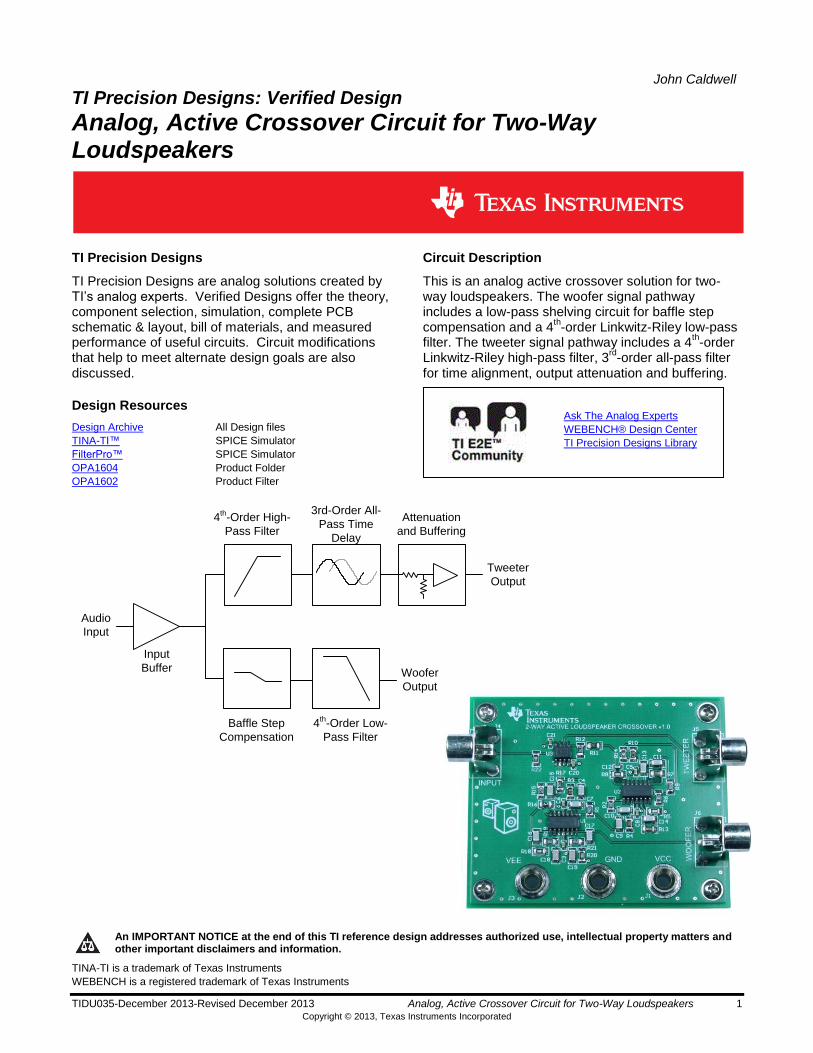
John Caldwell
TI Precision Designs: Verified Design
Analog, Active Crossover Circuit for Two-Way Loudspeakers
TI Precision Designs Circuit Description
TI Precision Designs are analog solutions created by TI’s analog experts. Verified Designs offer the theory, component selection, simulation, complete PCB schematic & layout, bill of materials, and measured performance of useful circuits. Circuit modifications that help to meet alternate design goals are also discussed.
This is an analog active crossover solution for two-way loudspeakers. The woofer signal pathway includes a low-pass shelving circuit for baffle step compensation and a 4
th-order Linkwitz-Riley low-pass
filter. The tweeter signal pathway includes a 4th-order
Linkwitz-Riley high-pass filter, 3rd
-order all-pass filter for time alignment, output attenuation and buffering.
Design Resources
Design Archive All Design files
TINA-TI™ SPICE Simulator
FilterPro™ SPICE Simulator
OPA1604 Product Folder
OPA1602 Product Filter
Ask The Analog Experts
WEBENCH® Design Center
TI Precision Designs Library
4th-Order High-
Pass Filter
3rd-Order All-
Pass Time
Delay
Attenuation
and Buffering
4th-Order Low-
Pass Filter
Baffle Step
Compensation
Input
Buffer
Tweeter
Output
Woofer
Output
Audio
Input

www.ti.com
2 Analog, Active Crossover Circuit for Two-Way Loudspeakers TIDU035-December 2013-Revised December 2013 Copyright © 2013, Texas Instruments Incorporated
1 Design Summary
The design requirements are as follows:
Supply Voltage: +/- 15 V
Input and Output Levels: +4dBu / 1.228Vrms
Crossover Frequency (Acoustic): 1.8kHz
Loudspeakers and Enclosure Dimensions: See Appendix
The design goals and performance are summarized in Table 1.
Figure 1 depicts the measured transfer function of the design.
Table 1. Comparison of Design Goals, Simulation, and Measured Performance
Specification Design Goal Simulation Measured
Baffle Step Compensation (at 650 Hz) 6 dB 5.96 dB 6.137 dB
Low-pass Filter Corner Frequency 2.145 kHz 2.1096 kHz 2.113 kHz
Tweeter Attenuation 8 dB 7.91 dB 8.04 dB
High-pass Filter Corner Frequency 1.8 kHz 1.746 kHz 1.737 kHz
Nominal Tweeter Delay 155 us 155.28 us 155.261 us
10% Degradation in Tweeter Delay >3.6 kHz 3.814 kHz 4.083 kHz
THD+N (100 Hz) <.01% 0.000146% 0.0003%
THD+N (10 kHz) <.01% 0.000484% 0.00128%
Figure 1: Measured Transfer Function of the crossover network.
-60
-50
-40
-30
-20
-10
0
10 100 1000 10000
Am
plitu
de (
dB
)
Frequency (Hz)
Transfer Function of Individual Outputs
Woofer Output
Tweeter Output

www.ti.com
TIDU035-December 2013-Revised December 2013 Analog, Active Crossover Circuit for Two-Way Loudspeakers 3 Copyright © 2013, Texas Instruments Incorporated
2 Theory of Operation
The primary purpose of the crossover circuit in a loudspeaker is to split an incoming audio signal into frequency bands that are passed to the speaker or “driver” best suited. For example, in a two-way system a crossover circuit will pass low frequencies to the woofer and high frequencies to the tweeter. This is accomplished using passive or active filters to remove frequencies outside of the desired band for a driver. A secondary purpose of crossover circuits is to correct the frequency or phase response of the system for errors introduced by the loudspeaker enclosure and listening environment.
Active crossover networks are commonly used in recording studios and some home high-fidelity systems. In an active crossover system, the crossover network is placed before the power amplifiers in the audio signal chain. The voltages at this point in the signal chain are much lower than those applied directly to the speaker, allowing the use of active filters which employ op-amps, capacitors, and resistors. Expensive passive components which must maintain linearity at high voltage levels can be eliminated from active crossover circuits. Furthermore, the filter circuits in an active crossover do not directly interact with the loudspeaker impedance, allowing them to more closely follow the desired transfer function without complicated analysis.
High-Pass Filter
Low-Pass Filter
Baffle Step
Compensation
All-Pass FilterTweeter Level
Correction
VCC
VEE
VCC
VEE
VCC
VEE
VCC
VEE
VCC
VEE
VCC
VEE
VCC
VEE
VCC
VEE
VCC
VEE
VCC
VEE
C4 C7
R1
R3
C9 C10
R2
R4
-
++U1A
-
+ +U2A
R5 R6
R13C14
R7
C13
C11
R14
R9
R10
R8
C12
-
++
U2B
-
++
U2C
-
++
U2D
R18 R19
C16
C18
R20 R21
C17
C19-
+ +U1D
-
+ +U1C
R17
R16
R15C15
-
+ +
U1B
Woofer
-
++U3A
R22+
VG1
R11
R12
-
+ +U3B
Tweeter
¼ OPA1604
¼ OPA1604
¼ OPA1604
¼ OPA1604
¼ OPA1604
¼ OPA1604
¼ OPA1604
¼ OPA1604
½ OPA1602½ OPA1602
100n 100n
100n 100n
100n
100n
100n
100n
100n100n
47n
47n
845
845
1k 1k
1k
1k
1.74k
1.15k
475
10p
221
422
332
1.30k
590
1.30k
590
11.8k
11.8k
11.8k
10k
1.4k
1.4k
Figure 2: Complete crossover network schematic with functional portions highlighted
This design can be broken into 5 parts which are shown in Figure 2. The signal path for the woofer output includes a baffle step compensation circuit and a low-pass filter. The tweeter portion includes a high-pass filter, an all-pass filter for time alignment, and output level correction. The design parameters are chosen to represent a typical two-way monitor speaker which may be employed in a small room such as a recording studio for near-field listening and sound mixing work.
Proper loudspeaker design requires the use of acoustic measurements during the design process. Each portion of the design theory section will incorporate raw acoustic measurements of the drivers installed in an enclosure and placed in the desired listening location. All measurements were made at a distance of 1m, on-axis with the tweeter. The plots presented use 1/8
th octave smoothing and the measurements were
un-gated unless otherwise noted. This was done to show the effects produced by the loudspeaker’s interaction with the listening environment.

www.ti.com
4 Analog, Active Crossover Circuit for Two-Way Loudspeakers TIDU035-December 2013-Revised December 2013 Copyright © 2013, Texas Instruments Incorporated
2.1 Baffle Step Compensation
Conventional speaker systems which use a “box” type enclosure will exhibit variations in the frequency response due to diffraction effects of the enclosure. A major contributor to these variations in the frequency response is diffraction from the front wall or “baffle” of the enclosure. At low frequencies, the wavelength of the sound being radiated is very large compared to the width of the enclosure; at these frequencies the speaker’s radiation pattern is essentially spherical. At higher frequencies, the wavelength of the sound being produced approaches the width of the front baffle, and the speaker begins to radiate in a hemispherical pattern [1]. Because the speaker is radiating the same amount of energy into half of the space, the sound intensity will increase by 6dB as the speaker transitions from radiating in a spherical pattern to a hemispherical pattern. This effect is commonly referred to as “baffle step” and visible in the rising frequency response of the woofer shown in Figure 3. This measurement was taken with the woofer in the enclosure and includes the effects of the listening room as well.
Figure 3: Woofer frequency response measured at a 1m distance on the tweeter axis (designed listening position). 1/8
th Octave smoothing is applied and no gating is used (includes room effects)
Software packages are available which can predict the diffraction effects of the enclosure. Figure 4 illustrates the predicted diffraction effects from mounting a 178 mm woofer, on a 216 mm x 356 mm baffle, 127 mm from the bottom edge. The 3dB point of the step is at 313Hz with an additional peak near 1000 Hz, which is a diffraction effect of the corners on the enclosure. Rounding these edges helps to reduce the amplitude of this peak.
The blue curve in Figure 4 depicts the diffraction effects in an anechoic environment. Most listening environments are not anechoic and have acoustically reflective surfaces which will cause further variations in the frequency response. The red curve shows an example of the effects of placing the loudspeaker in a small room with adjacent reflective surfaces.
The term “baffle step compensation” refers to techniques used to compensate for the rise in a speaker’s frequency response due to the changing radiation pattern. This can be accomplished by applying a specific amount of attenuation to input frequencies above the transition frequency.
-40
-35
-30
-25
-20
-15
-10
-5
0
5
10
10 100 1000 10000
Am
plitu
de (
dB
)
Frequency (Hz)
Woofer Frequency Response

www.ti.com
TIDU035-December 2013-Revised December 2013 Analog, Active Crossover Circuit for Two-Way Loudspeakers 5 Copyright © 2013, Texas Instruments Incorporated
Figure 4: Predicted baffle diffraction effects (blue curve) of a 178 mm woofer mounted on an 216 mm x 356 mm baffle (13 mm radius edge rounding). The center point of the woofer is 127 mm from the bottom edge. The red curve includes room acoustic effects as well. Curves generated by Baffle Diffraction and Boundary Simulator v1.2 © Jeff Bagby, used with permission.
The low-pass shelving circuit shown in Figure 5 can be used to compensate for this rise in amplitude response with increasing frequency. At low frequencies, the gain of the circuit is:
(1)
At high frequencies, when the impedance of the capacitor becomes very small, the gain of the circuit has been decreased:
(2)
This shelving behavior is illustrated by the red curve in Figure 6. A more generic form of the magnitude response for this circuit is:
| |
(3)
In order to properly design the baffle step compensation circuit, the woofer frequency response from Figure 3, was compared to a flat target response. A numerical solver algorithm compared the woofer frequency response to the target response for frequencies between 100Hz and 1kHz and determined the passive component values which provided the flattest response in this region. The final values are shown in Figure 5.
0
2
4
6
8
10
12
14
16
18
20
10 100 1000 10000
Am
plitu
de R
esp
on
se (
dB
)
Frequency (Hz)
Baffle Diffraction and Room Interaction Effects
Baffle Diffraction Combined Baffle Diffraction and Room Response

www.ti.com
6 Analog, Active Crossover Circuit for Two-Way Loudspeakers TIDU035-December 2013-Revised December 2013 Copyright © 2013, Texas Instruments Incorporated
VCC
VEE
R17
R16
R15C15
-
++
U1B
¼ OPA1604
100n 11.8k
11.8k
11.8k
From Input Buffer
To Low-Pass Filter
Figure 5: A shelving circuit used to compensate for the baffle diffraction step
The frequency response of the baffle step compensation circuit is shown in Figure 6 in red. The raw woofer response is shown in blue, and the corrected woofer response is shown in green.
Figure 6: Corrected woofer response including the effects of both the low-pass filter and shelving circuit
As can be seen in Figure 6, the gain at low-frequencies is 1 (0dB) because R16 and R17 are equal. At high frequencies the gain of the circuit is -6.0206dB:
( ) (4)
Using the component values shown in Figure 5, the -3dB point will be 95 Hz. The negative sign in the gain equation indicates that the polarity of the output signal has been reversed. In order to correct for this phase inversion, the woofer must be connected with reversed polarity to maintain proper phase orientation.
2.2 Low Pass Filter
For this design, the corner frequency for the woofer is 1.8kHz; a very common value for two-way loudspeakers of this size. The selection of this frequency is beyond the scope of this document and is a function of the woofer size, desired on-axis and off-axis frequency response, distortion characteristics, and proximity to the tweeter.
-40
-35
-30
-25
-20
-15
-10
-5
0
5
10
10 100 1000 10000
Am
plitu
de (
dB
)
Frequency (Hz)
Woofer Frequency Response with Baffle Step Compensation
Raw Woofer Response
Baffle Step Compensation
Corrected Woofer Response

www.ti.com
TIDU035-December 2013-Revised December 2013 Analog, Active Crossover Circuit for Two-Way Loudspeakers 7 Copyright © 2013, Texas Instruments Incorporated
The Linkwitz-Riley filter characteristic was selected because these filters sum acoustically flat in the crossover region [2]. A 4
th-order Linkwitz-Riley filter has a steep roll-off (48 dB/octave, 80 dB/decade)
which limits high-frequency distortion from the woofer, and protects the tweeter from low-frequency content which may damage it.
Although the desired corner frequency for the woofer transfer function is 1.8kHz, this does not necessarily mean the corner frequency for the low-pass filter will be 1.8kHz. Examining the woofer frequency response with baffle step compensation in Figure 7 (blue curve), shows that the driver itself begins to attenuate signals above 2kHz. Therefore, the 1.8kHz corner frequency specifies the acoustic transfer function, which is the combination of the low-pass filter transfer function with the driver’s frequency response.
Again, using a numerical solver, it was found that a 4th
-order low-pass filter with a corner frequency of 2.145kHz provided the desired acoustic corner frequency of 1.8kHz. Figure 8 shows the predicted acoustic transfer function of the woofer produced by multiplying the woofer frequency response (with baffle step compensation) by the transfer function of the filter.
Figure 7: Woofer frequency response including baffle step compensation (blue) and the target 4th
-order Linkwitz-Riley low-pass transfer function with 1.8 kHz corner frequency (black)
-70
-60
-50
-40
-30
-20
-10
0
10
10 100 1000 10000
Am
plitu
de (
dB
)
Frequency (Hz)
Target Woofer Response
Woofer Response w/BSCTarget Response

www.ti.com
8 Analog, Active Crossover Circuit for Two-Way Loudspeakers TIDU035-December 2013-Revised December 2013 Copyright © 2013, Texas Instruments Incorporated
Figure 8: The woofer's frequency response including the filter response (green). The filter frequency response is shown in red, target response in black, and woofer response with baffle step compensation (BSC) shown in blue
A 4th-order Linkwitz-Riley filter may be constructed by cascading two 2
nd-order Butterworth low-pass filters
as shown in Figure 9[2]. The Sallen-Key (SK) filter topology is used because the noise gain and signal gain for this topology are equal since the op amp is configured as a non-inverting amplifier. In the multiple feedback (MFB) topology, the op amp is configured as an inverting amplifier and its noise gain would be twice the signal gain for a unity gain filter, degrading the system signal to noise ratio.
VCC
VEE
VCC
VEE
R18 R19
C16
C18
R20 R21
C17
C19-
++U1D
-
+ +U1C
2nd
-Order Butterworth
Low-Pass Filter 2nd
-Order Butterworth
Low-Pass Filter
Figure 9: A 4th-Order Linkwitz-Riley low-pass filter made by cascading two 2nd
-order Butterworth low-pass filters
-70
-60
-50
-40
-30
-20
-10
0
10
10 100 1000 10000
Am
plitu
de (
dB
)
Frequency (Hz)
Filtered Woofer Frequency Response
Woofer Response w/BSC
Filter Response
Filtered Woofer Response
Target Response
www.ti.com
TIDU035-December 2013-Revised December 2013 Analog, Active Crossover Circuit for Two-Way Loudspeakers 9 Copyright © 2013, Texas Instruments Incorporated
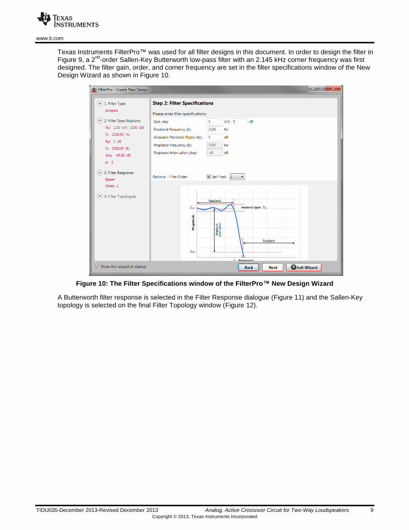
Texas Instruments FilterPro™ was used for all filter designs in this document. In order to design the filter in Figure 9, a 2
nd-order Sallen-Key Butterworth low-pass filter with an 2.145 kHz corner frequency was first
designed. The filter gain, order, and corner frequency are set in the filter specifications window of the New Design Wizard as shown in Figure 10.
Figure 10: The Filter Specifications window of the FilterPro™ New Design Wizard
A Butterworth filter response is selected in the Filter Response dialogue (Figure 11) and the Sallen-Key topology is selected on the final Filter Topology window (Figure 12).

www.ti.com
10 Analog, Active Crossover Circuit for Two-Way Loudspeakers TIDU035-December 2013-Revised December 2013 Copyright © 2013, Texas Instruments Incorporated
Figure 11: The Filter Response window of the FilterPro™ New Design Wizard
Figure 12: The Filter Topology window of the FilterPro™ New Design Wizard

www.ti.com
TIDU035-December 2013-Revised December 2013 Analog, Active Crossover Circuit for Two-Way Loudspeakers 11 Copyright © 2013, Texas Instruments Incorporated
The resulting passive component values will be “exact” values which do not conform to standard resistor and capacitor values. Figure 13 shows the design after changing the resistor tolerance to 1% and the capacitor tolerance to 10%. The value of C2 in Figure 13 was forced to 100nF and FilterPro™ calculated the resulting values of other circuit components. The 100nF value for C2 was selected after researching multiple suppliers revealed that this was the largest practical value for a C0G ceramic capacitor in a 1206 surface mount package. Choosing the largest available capacitor value allows for lower resistor values, reducing the thermal noise of the system and minimizing the input current noise contribution of the op amp.
Figure 13: Final 2nd
-order Butterworth low-pass filter design using 1% resistor tolerances and 10% capacitor tolerances. The value for C2 was forced to 100nF
Once the 2nd
-order Butterworth low-pass filter has been designed, the final 4th-order Linkwitz-Riley filter is
simply two cascaded 2nd
-order filters as shown in Figure 14. Finally, because this is a low-pass filter, it should be placed last in the woofer signal path. This will allow the filter to attenuate the high-frequency noise of the circuits before it, improving the system signal to noise ratio.
VCC
VEE
VCC
VEE
R18 R19
C16
C18
R20 R21
C17
C19-
++U1D
-
+ +U1C
¼ OPA1604
¼ OPA1604
100n100n
47n
47n
845
845
1.4k
1.4k
From Baffle Step
Compensation
To Woofer
Output
Figure 14: Final 1.8 kHz, 4th
-order Linkwitz-Riley low-pass filter
www.ti.com
12 Analog, Active Crossover Circuit for Two-Way Loudspeakers TIDU035-December 2013-Revised December 2013 Copyright © 2013, Texas Instruments Incorporated
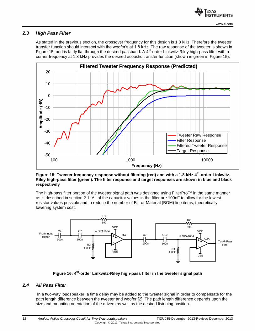
2.3 High Pass Filter
As stated in the previous section, the crossover frequency for this design is 1.8 kHz. Therefore the tweeter transfer function should intersect with the woofer’s at 1.8 kHz. The raw response of the tweeter is shown in Figure 15, and is fairly flat through the desired passband. A 4
th-order Linkwitz-Riley high-pass filter with a
corner frequency at 1.8 kHz provides the desired acoustic transfer function (shown in green in Figure 15).
Figure 15: Tweeter frequency response without filtering (red) and with a 1.8 kHz 4th
-order Linkwitz-Riley high-pass filter (green). The filter response and target responses are shown in blue and black respectively
The high-pass filter portion of the tweeter signal path was designed using FilterPro™ in the same manner as is described in section 2.1. All of the capacitor values in the filter are 100nF to allow for the lowest resistor values possible and to reduce the number of Bill-of-Material (BOM) line items, theoretically lowering system cost.
VCC
VEE
VCC
VEE
C4 C7
R1
R3
C9 C10
R2
R4
-
++U1A
-
+ +U2A
¼ OPA1604
¼ OPA1604
100n 100n
100n 100n
1.30k
590
1.30k
590
From Input
Buffer
To All-Pass
Filter
Figure 16: 4th
-order Linkwitz-Riley high-pass filter in the tweeter signal path
2.4 All Pass Filter
In a two-way loudspeaker, a time delay may be added to the tweeter signal in order to compensate for the path length difference between the tweeter and woofer [2]. The path length difference depends upon the size and mounting orientation of the drivers as well as the desired listening position.
-50
-40
-30
-20
-10
0
10
20
100 1000 10000
Am
pli
tud
e (
dB
)
Frequency (Hz)
Filtered Tweeter Frequency Response (Predicted)
Tweeter Raw Response
Filter Response
Filtered Tweeter Response
Target Response

www.ti.com
TIDU035-December 2013-Revised December 2013 Analog, Active Crossover Circuit for Two-Way Loudspeakers 13 Copyright © 2013, Texas Instruments Incorporated
A
BC
D
P
Figure 17: The path length geometry of a typical two-way loudspeaker
Figure 17 shows a cross section of a typical two-way loudspeaker and the relevant dimensions labeled. The distance from each driver to the listening position (labeled point P) is measured from its “acoustic center” which we will consider to be the top of the voice coil for both drivers. In order to calculate the tweeter time delay necessary to ensure proper phase alignment, the woofer path length C must first be calculated
√( ) (5)
The dimensions A, B, and D are the listening distance, driver center-to-center spacing, and the distance the woofer acoustic center is behind the front of the enclosure. These dimensions are summarized in Table 2.
Table 2: Dimensions for the diagram in Figure 17
Dimension Value (m)
A 1
B 0.1524
D 0.05
√( ) ( ) (6)
The difference in path length between the woofer and the tweeter is then:
(7)
Using 346.1 m/s as the speed of sound at 25°C, gives a delay value of:
(8)
This value may seem insignificant. However, consider that at the crossover frequency of 1.8 kHz, a 176 μs time delay contributes a 114.21° phase shift.
www.ti.com
14 Analog, Active Crossover Circuit for Two-Way Loudspeakers TIDU035-December 2013-Revised December 2013 Copyright © 2013, Texas Instruments Incorporated
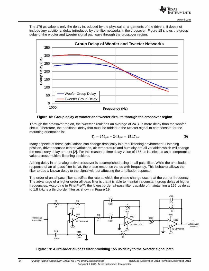
The 176 μs value is only the delay introduced by the physical arrangements of the drivers, it does not include any additional delay introduced by the filter networks in the crossover. Figure 18 shows the group delay of the woofer and tweeter signal pathways through the crossover region.
Figure 18: Group delay of woofer and tweeter circuits through the crossover region
Through the crossover region, the tweeter circuit has an average of 24.3 μs more delay than the woofer circuit. Therefore, the additional delay that must be added to the tweeter signal to compensate for the mounting orientation is:
(9)
Many aspects of these calculations can change drastically in a real listening environment. Listening position, driver acoustic center variations, air temperature and humidity are all variables which will change the necessary delay amount [2]. For this reason, a time delay value of 155 μs is selected as a compromise value across multiple listening positions.
Adding delay in an analog active crossover is accomplished using an all-pass filter. While the amplitude response of an all-pass filter is flat, the phase response varies with frequency. This behavior allows the filter to add a known delay to the signal without affecting the amplitude response.
The order of an all-pass filter specifies the rate at which the phase change occurs at the corner frequency. The advantage of a higher order all-pass filter is that it is able to maintain a constant group delay at higher frequencies. According to FilterPro™, the lowest-order all-pass filter capable of maintaining a 155 μs delay to 1.8 kHz is a third-order filter as shown in Figure 19.
VCC
VEE
VCC
VEE
VCC
VEE
R5 R6
R13C14
R7
C13
C11
R14
R9
R10
R8
C12
-
++
U2B
-
++
U2C
-
++
U2D¼ OPA1604
¼ OPA1604
¼ OPA1604
100n
100n
100n
1k 1k
1k
1k
475
10p
221
422
332
From High-
Pass Filter To
Attenuation
Network
Figure 19: A 3rd-order all-pass filter providing 155 us delay to the tweeter signal path
0
50
100
150
200
250
300
350
1000
Gro
up
Dela
y (
μs)
Frequency (Hz)
Group Delay of Woofer and Tweeter Networks
Woofer Group Delay
Tweeter Group Delay
www.ti.com
TIDU035-December 2013-Revised December 2013 Analog, Active Crossover Circuit for Two-Way Loudspeakers 15 Copyright © 2013, Texas Instruments Incorporated
All capacitor values were forced to 100nF and the resistor values were made as low as practical (1% tolerances are used). C12 is included to attenuate the noise contribution of amplifier U2D at frequencies above the audible range.
2.5 Level Control and Buffering
In general, speaker drivers which reproduce high frequencies are more efficient than those intended to reproduce low frequencies. “Sensitivity” is defined as the sound pressure level produced by the driver for a 1 W input signal (2.83 Vrms for an 8 Ohm driver) when measured at a 1 meter distance [1]. However, because loudspeakers are typically driven by a voltage source, it is more appropriate to compare their sound pressure levels for a certain input voltage. Table 3 compares the sound pressure level produced by the woofer and tweeter for a 2.83 Vrms input signal.
Table 3: Comparison of sound output
Driver Output Level (2.83V/1m)
Woofer 87 dB
Tweeter 91 dB
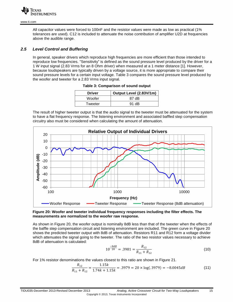
The result of higher tweeter output is that the audio signal to the tweeter must be attenuated for the system to have a flat frequency response. The listening environment and associated baffled step compensation circuitry also must be considered when calculating the amount of attenuation.
Figure 20: Woofer and tweeter individual frequency responses including the filter effects. The measurements are normalized to the woofer raw response.
As shown in Figure 20, the woofer output is nominally 8dB less than that of the tweeter when the effects of the baffle step compensation circuit and listening environment are included. The green curve in Figure 20 shows the predicted tweeter output with 8dB of attenuation. Resistors R11 and R12 form a voltage divider which attenuates the signal going to the tweeter. The ratio of the two resistor values necessary to achieve 8dB of attenuation is calculated:
(10)
For 1% resistor denominations the values closest to this ratio are shown in Figure 21.
( ) (11)
-60
-50
-40
-30
-20
-10
0
10
20
100 1000 10000
Am
plitu
de (
dB
)
Frequency (Hz)
Relative Output of Individual Drivers
Woofer Response Tweeter Response Tweeter Response (8dB attenuation)

www.ti.com
16 Analog, Active Crossover Circuit for Two-Way Loudspeakers TIDU035-December 2013-Revised December 2013 Copyright © 2013, Texas Instruments Incorporated
VCC
VEE
R11
R12
-
+ +U3B½ OPA16021.74k
1.15k
From All-
Pass Filter
To Tweeter
Output
Figure 21: Tweeter level correction and output buffer circuit.
A buffer is placed after the resistor network (U3B) in order to prevent the input impedance of any subsequent circuit in the signal path from affecting the attenuation factor. Likewise, the other half of dual op amp U3A is used as an input buffer to prevent the impedance of the source from affecting the individual filter transfer functions. The predicted loudspeaker frequency response is shown in Figure 22 along with the individual driver transfer functions. The predicted crossover point is 1.708 kHz.
Figure 22: Predicted loudspeaker frequency response (in room) with individual driver responses shown
-60
-50
-40
-30
-20
-10
0
10
10 100 1000 10000
Am
plitu
de (
dB
)
Frequency (Hz)
Predicted System Frequency Response
Woofer Response Tweeter Response (8dB attenuation) System Response

www.ti.com
TIDU035-December 2013-Revised December 2013 Analog, Active Crossover Circuit for Two-Way Loudspeakers 17 Copyright © 2013, Texas Instruments Incorporated
3 Component Selection
3.1 Amplifiers
The basic amplifier requirements for this system are summarized in Table 4. The power supply requirement is determined in the design summary. The gain bandwidth requirement is determined by FilterPro™ for proper filter functionality. Because the second stage of the all-pass filter requires the highest op-amp gain bandwidth of any filter stage, this value is determined to be the minimum for all amplifiers used in the system.
Table 4: Basic requirements for amplifiers used in the crossover network
Requirement Value
Max Power Supply >30V
Gain Bandwidth Product 180.3kHz
Slew Rate 2.2 V/μs
The slew rate requirement is calculated from the maximum slew rate of a sinusoid at 20kHz, and 1.228Vrms:
V/μs (12)
An amplifier with this slew rate limitation would contribute significant distortion at 20 kHz because the sinusoid would exhibit a triangular shape. A conservative design decision is to employ amplifiers with slew rates 10 times greater than the levels calculated in equation 12 in order to minimize distortion from slewing.
Table 5 shows a comparison of the cost, input voltage noise, power supply current, and measured THD+N of several quad op-amps which meet the above requirements and are intended for audio applications. The NE5532A and NE5534A are included in the table because these parts are ubiquitous in audio applications. It is often very difficult to justify the use of newer amplifiers given the high level of performance and low cost of the NE5532A and NE5534A.
Large capacitor values and low resistor values were selected in each portion of the circuit to minimize the thermal noise of the filter components and the impedance presented to the op amp inputs, reducing the contribution of amplifier input current noise to the total output noise. Therefore, bipolar input amplifiers are the preferred solution because the benefits of lower input voltage noise outweigh the increased current noise.
The OPA160x family of amplifiers was selected for this design because it is the lowest noise bipolar audio op amp that is available in a quad package (4-amplifiers in one package). Furthermore, the OPA160x family consumes significantly lower power supply current than the next lowest noise option, the LME49740. High-fidelity audio systems may involve a significant number of operational amplifiers and any additional supply current consumption may increase the cost of the power supply solution.
Table 5: A comparison of low noise bipolar op-amps commonly used in audio applications
Amplifier Amplifiers
per Package
Cost per Amplifier (1ku
prices)
Vn (nV/√Hz,
1kHz)
Power Supply Current (typ mA /
amplifier)
THD+N (1kHz, G=+1, 3Vrms, 600 Ohm
load)
NE5534A 1 $0.50 3.5 4 0.002%
NE5532A 2 $0.25 5 4 N/A
OPA1604 4 $0.49 2.5 2.8 0.00003%
OPA1664 4 $0.36 3.3 1.5 0.00006%
LME49740 4 $0.43 2.7 4.625 0.00003%
LME49743 4 $0.29 3.5 2.5 0.0001%

www.ti.com
18 Analog, Active Crossover Circuit for Two-Way Loudspeakers TIDU035-December 2013-Revised December 2013 Copyright © 2013, Texas Instruments Incorporated
The THD+N performance of the OPA160x family is shown in Figure 23. It is important to notice that there is little difference between the curves for inverting and non-inverting configurations, indicating that the part resists common-mode distortion. This is an important consideration in Sallen-Key filters where the part is configured as a non-inverting amplifier [2].
Figure 23: Measured THD+N performance of the OPA160x family of amplifiers for multiple gains and loading conditions.
Low impedance loads will increase the distortion produced by any amplifier because the output stage becomes less-linear as it is forced to deliver greater amounts of current. At high frequencies, this distortion becomes more apparent where there is less loop gain available to correct for output stage distortion through negative feedback. For this reason, the resistor values cannot be reduced to extremely low values in the pursuit of increased fidelity.
3.2 Passive Components
Proper selection of passive components is absolutely crucial to achieving low levels of distortion in active filters. High-K ceramic and electrolytic capacitors are not suitable for active filter circuits because they introduce significant amounts of odd-order harmonic distortion. This effect has been shown in numerous publications [2, 3, 4, 5].
The only capacitor types suitable for active filters are C0G ceramic, polypropylene film, or silvered mica. However, because silvered mica capacitors are not available in large capacitances they are not considered here. When comparing C0G ceramic capacitors to polypropylene film types, it was found that for the same tolerance, C0G ceramics were cheaper and occupied less board area than film types of the same capacitance.
Table 6: A Comparison of C0G ceramic to polypropylene film capacitors
Capacitor Type Tolerance Board Area (mm2) Cost (Each, Qty: 100)
NP0/C0G (1206) 5% 5.12 $0.33
Polypropylene Film 5% 65 $0.44
1206 surface mount packages (120mil x 60 mil) were chosen for both resistors and capacitors. The 1206 package was the smallest package in which a 100nF C0G capacitor was available.
Distortion issues have also been reported for surface mount resistors in extremely small packages and with certain resistive materials [2,5]. Testing for this design showed that thick film resistors in 1206 packages produced no measurable distortion at the signal levels commonly found in line-level audio equipment.

www.ti.com
TIDU035-December 2013-Revised December 2013 Analog, Active Crossover Circuit for Two-Way Loudspeakers 19 Copyright © 2013, Texas Instruments Incorporated
4 Simulation
4.1 Woofer Signal Path
The woofer signal path is composed of the baffle step compensation circuit and 4th-order low-pass filter
and the Tina-TI™ simulation schematic is shown in Figure 24.
Figure 24: Tina-TI™ simulation schematic of the woofer signal path
4.1.1 Transfer Function
Performing an AC Transfer Characteristic simulation in Tina-TI™ shows the transfer function of the woofer signal path. Because Linkwitz-Riley filters are defined by the -6dB point, the corner frequency shown in Figure 25 includes 6dB of attenuation from the low-pass filter as well as 6dB of attenuation from the baffle step compensation circuit. The simulated attenuation was 5.96 dB at 650 Hz and the corner frequency was 2.1096 kHz.
Figure 25: Tina-TI™ Simulation of the woofer signal path transfer function.
www.ti.com
20 Analog, Active Crossover Circuit for Two-Way Loudspeakers TIDU035-December 2013-Revised December 2013 Copyright © 2013, Texas Instruments Incorporated
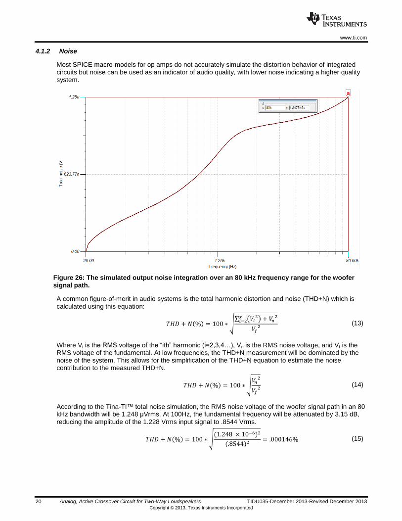
4.1.2 Noise
Most SPICE macro-models for op amps do not accurately simulate the distortion behavior of integrated circuits but noise can be used as an indicator of audio quality, with lower noise indicating a higher quality system.
Figure 26: The simulated output noise integration over an 80 kHz frequency range for the woofer signal path.
A common figure-of-merit in audio systems is the total harmonic distortion and noise (THD+N) which is calculated using this equation:
( ) √∑ (
)
(13)
Where Vi is the RMS voltage of the “ith” harmonic (i=2,3,4…), Vn is the RMS noise voltage, and Vf is the RMS voltage of the fundamental. At low frequencies, the THD+N measurement will be dominated by the noise of the system. This allows for the simplification of the THD+N equation to estimate the noise contribution to the measured THD+N.
( ) √
(14)
According to the Tina-TI™ total noise simulation, the RMS noise voltage of the woofer signal path in an 80 kHz bandwidth will be 1.248 μVrms. At 100Hz, the fundamental frequency will be attenuated by 3.15 dB, reducing the amplitude of the 1.228 Vrms input signal to .8544 Vrms.
( ) √( )
( ) (15)

www.ti.com
TIDU035-December 2013-Revised December 2013 Analog, Active Crossover Circuit for Two-Way Loudspeakers 21 Copyright © 2013, Texas Instruments Incorporated
4.2 Tweeter Signal Path
The tweeter section is composed of the 4th-order high-pass filter, 3
rd-order all-pass filter, and the output
attenuator and buffer.
Figure 27: TINA-TI™ simulation schematic of the tweeter signal path.
4.2.1 Transfer Function
An AC Transfer Characteristic was used to simulate the transfer function of the tweeter signal path. The simulation shows 7.91dB of attenuation in the passband and a corner frequency of 1.746 kHz.
Figure 28: TINA-TI simulation of the tweeter signal path transfer function.

www.ti.com
22 Analog, Active Crossover Circuit for Two-Way Loudspeakers TIDU035-December 2013-Revised December 2013 Copyright © 2013, Texas Instruments Incorporated
4.2.2 Noise
A total noise simulation was performed in TINA-TI™ to predict the noise contribution to the measured THD+N value.
Figure 29: Tina-TI™ total noise simulation of the tweeter signal path.
According to the noise simulation, the RMS noise voltage of the tweeter signal path in an 80 kHz bandwidth will be 2.369 μVrms. The significant increase in noise is due to the greater number of op amp circuits in the tweeter signal path. A 10 kHz, 1.228Vrms input signal will be attenuated by 8dB, reducing the fundamental to .489 Vrms, giving a predicted THD+N at 10 kHz of:
( ) √( )
( ) (16)
This number is very optimistic because the measured THD+N at high frequencies will be dominated by distortion harmonics rather than the noise voltage.
4.2.3 Tweeter Signal Delay
The 3rd
-order all-pass filter circuit can be tested by selecting the “Group Delay” option in the AC Transfer Characteristic options window.

www.ti.com
TIDU035-December 2013-Revised December 2013 Analog, Active Crossover Circuit for Two-Way Loudspeakers 23 Copyright © 2013, Texas Instruments Incorporated
Figure 30: Tina-TI™ simulation schematic for testing all-pass filter delay.
A 3rd
-order all-pass filter is not able to maintain the necessary delay for the entire audible bandwidth. However, it is preferable that significant reduction in the delay occur at least an octave above the 1.8 kHz crossover point of the system. A 10% reduction in delay has been used in other literature as a reference point for significant delay reduction [2].
Figure 31: Tina-TI™ simulation of the all-pass filter group delay.
The simulated nominal group delay of the all-pass filter circuit is 155.28 μs and falls to 90% of this value at 3.814kHz.
www.ti.com
24 Analog, Active Crossover Circuit for Two-Way Loudspeakers TIDU035-December 2013-Revised December 2013 Copyright © 2013, Texas Instruments Incorporated
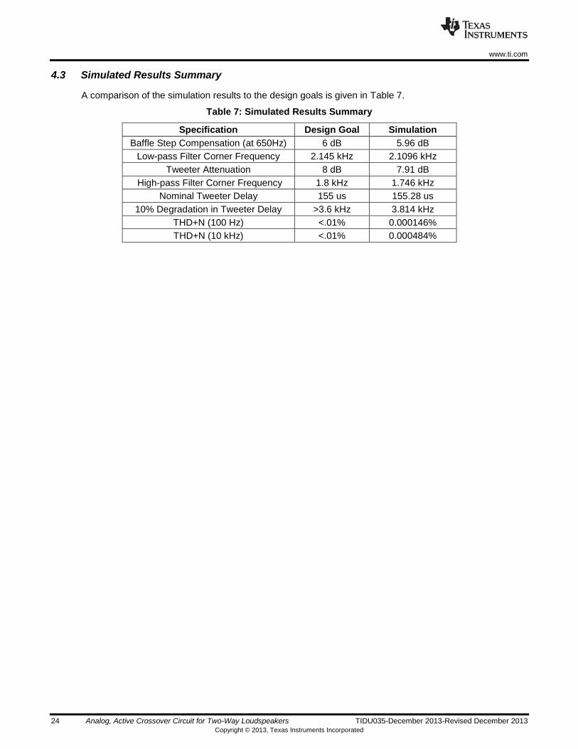
4.3 Simulated Results Summary
A comparison of the simulation results to the design goals is given in Table 7.
Table 7: Simulated Results Summary
Specification Design Goal Simulation
Baffle Step Compensation (at 650Hz) 6 dB 5.96 dB
Low-pass Filter Corner Frequency 2.145 kHz 2.1096 kHz
Tweeter Attenuation 8 dB 7.91 dB
High-pass Filter Corner Frequency 1.8 kHz 1.746 kHz
Nominal Tweeter Delay 155 us 155.28 us
10% Degradation in Tweeter Delay >3.6 kHz 3.814 kHz
THD+N (100 Hz) <.01% 0.000146%
THD+N (10 kHz) <.01% 0.000484%

www.ti.com
TIDU035-December 2013-Revised December 2013 Analog, Active Crossover Circuit for Two-Way Loudspeakers 25 Copyright © 2013, Texas Instruments Incorporated
5 PCB Design
The PCB schematic and bill of materials can be found in the Appendix.
5.1 PCB Layout
Standard low-noise PCB layout practices are required to achieve a high level of performance in audio designs. Specifically for this design, a primary concern is minimizing the signal path length and loop areas of the filter circuits. This helps to prevent extrinsic interference from entering the audio signal path. To accomplish this goal, careful consideration must be given to which op amp in each quad package is used for every circuit. For example, the first op amp in both signal paths are in the same package (U1A, U1B) to allow for more efficient routing of the input signal. As usual, bypass capacitors must be placed as close as possible to the op amp power supply pins and are connected to a low-impedance pathway to ground.
Figure 32: Top layer (left) and bottom layer (right) views of the PCB.

www.ti.com
26 Analog, Active Crossover Circuit for Two-Way Loudspeakers TIDU035-December 2013-Revised December 2013 Copyright © 2013, Texas Instruments Incorporated
6 Verification & Measured Performance
6.1 Electrical Measurements
6.1.1 Woofer Signal Path Transfer Function
The woofer signal path transfer function was measured using an industry standard audio analyzer. The measured baffle step compensation was 6.137 dB and the corner frequency was 2.113 kHz; very close to the simulated values.
Figure 33: Measured transfer function of the woofer signal path
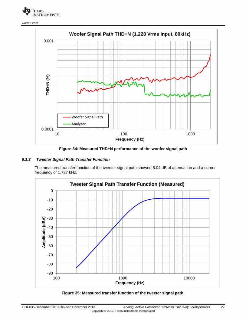
6.1.2 THD+N Performance – Woofer Output
The THD+N performance of the woofer signal path was measured using an audio analyzer with a measurement bandwidth of 80 kHz and a 1.228 Vrms (0 dBu) input signal level. THD+N measurements are only displayed within the passband of the specific filter. In the stop band of the filter, the attenuation of the input signal has the effect of increasing the measured THD+N (see equation 13).
The instrument measurement floor is displayed as the green curve in Figure 34. Because the woofer signal path includes a low-pass filter, it also attenuates the high-frequency noise of the analyzer. This is why the measured THD+N of the woofer signal pathway is below the instrument floor for frequencies less than 800 Hz. At 100 Hz, the measured THD+N is .0003%. This is more likely the noise floor of the instrument and not the actual distortion of the woofer signal pathway.
-90
-80
-70
-60
-50
-40
-30
-20
-10
0
10 100 1000 10000
Am
plitu
de (
dB
V)
Frequency (Hz)
Woofer Signal Path Transfer Function (Measured)
www.ti.com
TIDU035-December 2013-Revised December 2013 Analog, Active Crossover Circuit for Two-Way Loudspeakers 27 Copyright © 2013, Texas Instruments Incorporated
Figure 34: Measured THD+N performance of the woofer signal path
6.1.3 Tweeter Signal Path Transfer Function
The measured transfer function of the tweeter signal path showed 8.04 dB of attenuation and a corner frequency of 1.737 kHz.
Figure 35: Measured transfer function of the tweeter signal path.
0.0001
0.001
10 100 1000
TH
D+
N (
%)
Frequency (Hz)
Woofer Signal Path THD+N (1.228 Vrms Input, 80kHz)
Woofer Signal Path
Analyzer
-90
-80
-70
-60
-50
-40
-30
-20
-10
0
100 1000 10000
Am
plitu
de (
dB
V)
Frequency (Hz)
Tweeter Signal Path Transfer Function (Measured)

www.ti.com
28 Analog, Active Crossover Circuit for Two-Way Loudspeakers TIDU035-December 2013-Revised December 2013 Copyright © 2013, Texas Instruments Incorporated
6.1.4 Tweeter Signal Path THD+N
As expected, the greater number of op-amps in the tweeter signal pathway does degrade the THD+N performance slightly. The measured THD+N at 10 kHz is .00128% which is significantly below the design goal.
Figure 36: Measured THD+N of the tweeter signal path.
6.1.5 All-pass Filter Group Delay
The group delay of the all-pass filter in the tweeter signal path can be calculated from phase measurements using the relationship:
(17)
Where θ is the unwrapped phase in degrees and f is the frequency in Hz.
Figure 37: The group delay of the all-pass filter was calculated from a phase measurement
0.0001
0.001
0.01
1000 10000
TH
D+
N (
%)
Frequency (Hz)
Tweeter Signal Path THD+N (1.228 Vrms Input, 80 kHz)
Tweeter Signal Path
Analyzer
0.0E+00
2.0E-05
4.0E-05
6.0E-05
8.0E-05
1.0E-04
1.2E-04
1.4E-04
1.6E-04
1.8E-04
10 100 1000 10000
Gro
up
Dela
y (
s)
Frequency (Hz)
All-pass Filter Group Delay

www.ti.com
TIDU035-December 2013-Revised December 2013 Analog, Active Crossover Circuit for Two-Way Loudspeakers 29 Copyright © 2013, Texas Instruments Incorporated
6.2 Acoustic Measurements
The acoustic transfer functions of the drivers were measured using a calibrated measurement microphone, at a distance of 1m, on-axis with the tweeter. The measurements are taken un-gated to show the effects of the listening environment, except where noted. A diagram of the measurement setup is given in Appendix C.
6.2.1 Woofer Acoustic Transfer Function
The negative -6dB point of the woofer acoustic transfer function is 1725Hz.
Figure 38: Predicted and measured acoustic transfer function of the woofer. 1/8th octave smoothing
-60
-50
-40
-30
-20
-10
0
10
10 100 1000 10000
Am
plitu
de (
dB
)
Frequency (Hz)
Predicted and Measured Woofer Frequency Response
Predicted Woofer Response
Measured Woofer Response

www.ti.com
30 Analog, Active Crossover Circuit for Two-Way Loudspeakers TIDU035-December 2013-Revised December 2013 Copyright © 2013, Texas Instruments Incorporated
6.2.2 Tweeter Acoustic Transfer Function
The measured -6dB point of the tweeter acoustic transfer function was 1.5kHz.
Figure 39: Predicted and measured acoustic transfer function of the tweeter (1/8th octave smoothing) Ambient noise in the measurement environment affects the results below -40dB
6.2.3 System Frequency Response
The measured system frequency response closely matches the predicted response over much of the frequency range. A small hump is apparent near the crossover frequency. This is because the -6dB point of the tweeter response is lower than anticipated, causing a region of overlapping response from the woofer and tweeter.
Figure 40: Predicted and measured system frequency response.
-60
-50
-40
-30
-20
-10
0
10
100 1000 10000
Am
plitu
de (
dB
)
Frequency (Hz)
Predicted and Measured Tweeter Frequency Response
Predicted Tweeter Response
Measured Tweeter Response
-60
-50
-40
-30
-20
-10
0
10
10 100 1000 10000
Am
pli
tud
e (
dB
)
Frequency (Hz)
Predicted and Measured System Frequency Response
Measured System Response
Predicted System Response

www.ti.com
TIDU035-December 2013-Revised December 2013 Analog, Active Crossover Circuit for Two-Way Loudspeakers 31 Copyright © 2013, Texas Instruments Incorporated
6.2.4 Phase Alignment Testing
Inverting the phase of one of the drivers is a test commonly used to confirm proper phase alignment of the drivers in a loudspeaker at the crossover frequency. By inverting the phase of one of the drivers, a 180 degree phase shift is introduced to that driver’s output, causing destructive interference at the crossover frequency. This test verifies that when the drivers are connected with correct polarity, their outputs are in-phase at the crossover frequency. Gating is used to remove the effects of reflected sound from the listening room. For this reason, the displayed frequency response below 500 Hz is inaccurate. The inverted polarity connection produced a 25dB notch at 1.6 kHz.
Figure 41: Acoustic measurement of the loudspeaker with drivers connected in-phase and inverted phase. Connecting in inverted phase produces a 25 dB notch at 1.6 kHz.
6.3 Measured Results Summary
The measured results satisfy the design goals meet or exceed the design goals in most categories.
Table 8: A comparison of the measured results to the design goals.
Specification Design Goal Measured
Baffle Step Compensation (at 650Hz) 6 dB 6.137 dB
Low-pass Filter Corner Frequency 2.145 kHz 2.113 kHz
Tweeter Attenuation 8 dB 8.04 dB
High-pass Filter Corner Frequency 1.8 kHz 1.737 kHz
Nominal Tweeter Delay 155 us 155.261 us
10% Degradation in Tweeter Delay >3.6 kHz 4.083 kHz
THD+N (100 Hz) <.01% 0.0003%
THD+N (10 kHz) <.01% 0.00128%
-60
-50
-40
-30
-20
-10
0
10
100 1000 10000
Am
plitu
de (
dB
)
Frequency (Hz)
Inverted Woofer Polarity
Correct Phase
Inverted Phase

www.ti.com
32 Analog, Active Crossover Circuit for Two-Way Loudspeakers TIDU035-December 2013-Revised December 2013 Copyright © 2013, Texas Instruments Incorporated
7 Modifications
Increased resistances and lower capacitances may be desired in the filter sections for reasons of cost and board area. In this case, FET input amplifiers may offer improved performance due to their low input current noise. However, FET input amplifiers are more susceptible to distortion when placed in a non-inverting configuration such as a Sallen-Key filter. Therefore, a compromise must be made between cost, noise, and harmonic distortion. Two FET-input amplifiers which are suitable for this design due to their exceptional audio performance and availability in quad packages are given in Table 9.
Table 9: FET input amplifiers which offer lower input current noise and are suitable for use with larger resistance values.
Amplifier Amplifiers
per Package
Cost per Amplifier
(1ku prices)
Vn (nV/rtHz,
1kHz)
Power Supply Current (typ mA /
amplifier)
THD+N (1kHz, G=+1, 3Vrms, 600 Ohm load)
OPA1644 4 $0.49 5.1 2.3 0.00006%
OPA1652 4 $0.24 4.5 2 0.00008%
8 About the Author
John Caldwell is an applications engineer with Texas Instruments Precision Analog, supporting operational amplifiers and industrial linear devices. He specializes in precision circuit design for sensors, low-noise design and measurement, and electromagnetic interference issues. He received his MSEE and BSEE from Virginia Tech with a research focus on biomedical electronics and instrumentation. Prior to joining TI in 2010, John worked at Danaher Motion and Ball Aerospace.

www.ti.com
TIDU035-December 2013-Revised December 2013 Analog, Active Crossover Circuit for Two-Way Loudspeakers 33 Copyright © 2013, Texas Instruments Incorporated
9 References
1. V. Dickason, The Loudspeaker Design Cookbook: Sixth Edition. Audio Amateur Press, 2000.
2. D. Self, The Design of Active Crossover. Elsevier/ Focal Press,2011.
3. D. Self, Small Signal Audio Design. Elsevier/ Focal Press,2010.
4. J. Caldwell. (2013, June 16). Signal Distortion from High-K Ceramic Capacitors. Available: http://www.edn.com/design/analog/4416466/Signal-distortion-from-high-K-ceramic-capacitors
5. B. Hofer. Designing for Ultra-Low THD+N. Audio Express, December 2013.

www.ti.com
34 Analog, Active Crossover Circuit for Two-Way Loudspeakers TIDU035-December 2013-Revised December 2013 Copyright © 2013, Texas Instruments Incorporated
Appendix A.
A.1 Electrical Schematic
Figure A-1: Electrical Schematic

www.ti.com
TIDU035-December 2013-Revised December 2013 Analog, Active Crossover Circuit for Two-Way Loudspeakers 35 Copyright © 2013, Texas Instruments Incorporated
A.2 Bill of Materials
Quantity Value Designator Description Manufacturer Manufacturer Part # Supplier Part #
2 4.7uF C1, C2 CAP, CERM, 4.7uF, 16V, +/-10%, X5R,
1206 Kemet C1206C475K4PACTU 4520506
6 0.1uF C3, C5, C6, C8,
C20, C21 CAP, CERM, 0.1uF,
16V, +/-5%, X7R, 0603 AVX 0603YC104JAT2A 478-3726-1-ND
10 0.1uF C4, C7, C9, C10, C11, C13, C14, C15, C16, C17
CAP, CERM, 0.1uF, 25V, +/-5%, C0G/NP0,
1206 TDK C3216C0G1E104J 445-2691-1-ND
1 10pF C12 CAP, CERM, 10pF,
50V, +/-5%, C0G/NP0, 0603
AVX 06035A100JAT2A 478-1163-1-ND
2 0.047uF C18, C19 CAP, CERM, 0.047uF, 50V, +/-5%, C0G/NP0,
1206 MuRata GRM31M5C1H473JA01L 490-1764-1-ND
3
J1, J2, J3 Standard Banana Jack,
Uninsulated, 5.5mm Keystone 575-4 575-4K-ND
3
J4, J5, J6 RCA Jack, Metal, Right
Angle CUI Inc RCJ-011 CP-1400-ND
2 590 R1, R2 RES, 590 ohm, 1%,
0.25W, 1206 Vishay-Dale CRCW1206590RFKEA 541-590FCT-ND
2 1.30k R3, R4 RES, 1.30k ohm, 1%,
0.25W, 1206 Vishay-Dale CRCW12061K30FKEA 541-1.30KFCT-ND
4 1.00k R5, R6, R8, R14 RES, 1.00k ohm, 1%,
0.25W, 1206 Vishay-Dale CRCW12061K00FKEA 541-1.00KFCT-ND
1 422 R7 RES, 422 ohm, 1%,
0.25W, 1206 Vishay-Dale CRCW1206422RFKEA 541-422FCT-ND
1 221 R9 RES, 221 ohm, 1%,
0.25W, 1206 Vishay-Dale CRCW1206221RFKEA 541-221FCT-ND
1 475 R10 RES, 475 ohm, 1%,
0.25W, 1206 Vishay-Dale CRCW1206475RFKEA 541-475FCT-ND
1 1.74k R11 RES, 1.74k ohm, 1%,
0.25W, 1206 Vishay-Dale CRCW12061K74FKEA 541-1.74KFCT-ND
1 1.15k R12 RES, 1.15k ohm, 1%,
0.25W, 1206 Vishay-Dale CRCW12061K15FKEA 541-1.15KFCT-ND
1 332 R13 RES, 332 ohm, 1%,
0.25W, 1206 Vishay-Dale CRCW1206332RFKEA 541-332FCT-ND
3 11.8k R15, R16, R17 RES, 11.8k ohm, 1%,
0.25W, 1206 Vishay-Dale CRCW120611K8FKEA 541-11.8KFCT-ND
2 845 R18, R20 RES, 845 ohm, 1%,
0.25W, 1206 Vishay-Dale CRCW1206845RFKEA 541-845FCT-ND
2 1.40k R19, R21 RES, 1.40k ohm, 1%,
0.25W, 1206 Vishay-Dale CRCW12061K40FKEA 541-1.40KFCT-ND
1 10.0k R22 RES, 10.0k ohm, 1%,
0.25W, 1206 Vishay-Dale CRCW120610K0FKEA 541-10.0KFCT-ND
2
U1, U2 Quad, Low Noise, Audio Operational
Amplifier
Texas Instruments
OPA1604AIDR 296-30115-1-ND
1
U3 Dual, Low Noise, Audio Operational Amplifier
Texas Instruments
OPA1602AID 296-28930-5-ND
Figure A-2: Bill of Materials
www.ti.com
36 Analog, Active Crossover Circuit for Two-Way Loudspeakers TIDU035-December 2013-Revised December 2013 Copyright © 2013, Texas Instruments Incorporated
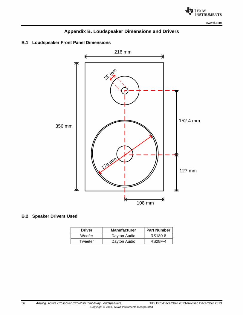
Appendix B. Loudspeaker Dimensions and Drivers
B.1 Loudspeaker Front Panel Dimensions
152.4 mm
216 mm
127 mm
356 mm
108 mm
178 mm
25 mm
B.2 Speaker Drivers Used
Driver Manufacturer Part Number
Woofer Dayton Audio RS180-8
Tweeter Dayton Audio RS28F-4

www.ti.com
TIDU035-December 2013-Revised December 2013 Analog, Active Crossover Circuit for Two-Way Loudspeakers 37 Copyright © 2013, Texas Instruments Incorporated
Appendix C. Acoustic Measurement Setup
1 m
Microphone
PreamplifierSpeaker
Under Test
Audio Power
Amplifier
Calibrated
Microphone
Full Duplex
Sound CardCrossover
Circuit
Line Out
Line In
Woofer
Output
Tweeter
Output
Computer with Acoustic
Measurement Software
Figure 42: Conceptual diagram of the equipment used for the acoustic measurements in this document. The crossover circuit is omitted for raw driver measurements.
Figure 43: The loudspeaker under test with a calibrated measurement microphone placed on the tweeter axis at a 1 m distance.

IMPORTANT NOTICE FOR TI REFERENCE DESIGNS
Texas Instruments Incorporated ("TI") reference designs are solely intended to assist designers (“Buyers”) who are developing systems thatincorporate TI semiconductor products (also referred to herein as “components”). Buyer understands and agrees that Buyer remainsresponsible for using its independent analysis, evaluation and judgment in designing Buyer’s systems and products.
TI reference designs have been created using standard laboratory conditions and engineering practices. TI has not conducted anytesting other than that specifically described in the published documentation for a particular reference design. TI may makecorrections, enhancements, improvements and other changes to its reference designs.
Buyers are authorized to use TI reference designs with the TI component(s) identified in each particular reference design and to modify thereference design in the development of their end products. HOWEVER, NO OTHER LICENSE, EXPRESS OR IMPLIED, BY ESTOPPELOR OTHERWISE TO ANY OTHER TI INTELLECTUAL PROPERTY RIGHT, AND NO LICENSE TO ANY THIRD PARTY TECHNOLOGYOR INTELLECTUAL PROPERTY RIGHT, IS GRANTED HEREIN, including but not limited to any patent right, copyright, mask work right,or other intellectual property right relating to any combination, machine, or process in which TI components or services are used.Information published by TI regarding third-party products or services does not constitute a license to use such products or services, or awarranty or endorsement thereof. Use of such information may require a license from a third party under the patents or other intellectualproperty of the third party, or a license from TI under the patents or other intellectual property of TI.
TI REFERENCE DESIGNS ARE PROVIDED "AS IS". TI MAKES NO WARRANTIES OR REPRESENTATIONS WITH REGARD TO THEREFERENCE DESIGNS OR USE OF THE REFERENCE DESIGNS, EXPRESS, IMPLIED OR STATUTORY, INCLUDING ACCURACY ORCOMPLETENESS. TI DISCLAIMS ANY WARRANTY OF TITLE AND ANY IMPLIED WARRANTIES OF MERCHANTABILITY, FITNESSFOR A PARTICULAR PURPOSE, QUIET ENJOYMENT, QUIET POSSESSION, AND NON-INFRINGEMENT OF ANY THIRD PARTYINTELLECTUAL PROPERTY RIGHTS WITH REGARD TO TI REFERENCE DESIGNS OR USE THEREOF. TI SHALL NOT BE LIABLEFOR AND SHALL NOT DEFEND OR INDEMNIFY BUYERS AGAINST ANY THIRD PARTY INFRINGEMENT CLAIM THAT RELATES TOOR IS BASED ON A COMBINATION OF COMPONENTS PROVIDED IN A TI REFERENCE DESIGN. IN NO EVENT SHALL TI BELIABLE FOR ANY ACTUAL, SPECIAL, INCIDENTAL, CONSEQUENTIAL OR INDIRECT DAMAGES, HOWEVER CAUSED, ON ANYTHEORY OF LIABILITY AND WHETHER OR NOT TI HAS BEEN ADVISED OF THE POSSIBILITY OF SUCH DAMAGES, ARISING INANY WAY OUT OF TI REFERENCE DESIGNS OR BUYER’S USE OF TI REFERENCE DESIGNS.
TI reserves the right to make corrections, enhancements, improvements and other changes to its semiconductor products and services perJESD46, latest issue, and to discontinue any product or service per JESD48, latest issue. Buyers should obtain the latest relevantinformation before placing orders and should verify that such information is current and complete. All semiconductor products are soldsubject to TI’s terms and conditions of sale supplied at the time of order acknowledgment.
TI warrants performance of its components to the specifications applicable at the time of sale, in accordance with the warranty in TI’s termsand conditions of sale of semiconductor products. Testing and other quality control techniques for TI components are used to the extent TIdeems necessary to support this warranty. Except where mandated by applicable law, testing of all parameters of each component is notnecessarily performed.
TI assumes no liability for applications assistance or the design of Buyers’ products. Buyers are responsible for their products andapplications using TI components. To minimize the risks associated with Buyers’ products and applications, Buyers should provideadequate design and operating safeguards.
Reproduction of significant portions of TI information in TI data books, data sheets or reference designs is permissible only if reproduction iswithout alteration and is accompanied by all associated warranties, conditions, limitations, and notices. TI is not responsible or liable forsuch altered documentation. Information of third parties may be subject to additional restrictions.
Buyer acknowledges and agrees that it is solely responsible for compliance with all legal, regulatory and safety-related requirementsconcerning its products, and any use of TI components in its applications, notwithstanding any applications-related information or supportthat may be provided by TI. Buyer represents and agrees that it has all the necessary expertise to create and implement safeguards thatanticipate dangerous failures, monitor failures and their consequences, lessen the likelihood of dangerous failures and take appropriateremedial actions. Buyer will fully indemnify TI and its representatives against any damages arising out of the use of any TI components inBuyer’s safety-critical applications.
In some cases, TI components may be promoted specifically to facilitate safety-related applications. With such components, TI’s goal is tohelp enable customers to design and create their own end-product solutions that meet applicable functional safety standards andrequirements. Nonetheless, such components are subject to these terms.
No TI components are authorized for use in FDA Class III (or similar life-critical medical equipment) unless authorized officers of the partieshave executed an agreement specifically governing such use.
Only those TI components that TI has specifically designated as military grade or “enhanced plastic” are designed and intended for use inmilitary/aerospace applications or environments. Buyer acknowledges and agrees that any military or aerospace use of TI components thathave not been so designated is solely at Buyer's risk, and Buyer is solely responsible for compliance with all legal and regulatoryrequirements in connection with such use.
TI has specifically designated certain components as meeting ISO/TS16949 requirements, mainly for automotive use. In any case of use ofnon-designated products, TI will not be responsible for any failure to meet ISO/TS16949.
Mailing Address: Texas Instruments, Post Office Box 655303, Dallas, Texas 75265Copyright © 2013, Texas Instruments Incorporated