Embed Size (px)
Citation preview

November 2013 DocID025039 Rev 1 1/27
AN4339Application note
BLDC motor based ceiling fan solution proposal
Harjeet Singh
Introduction
Due to recent directives by the “Bureau of Energy Efficiency” (BEE) to reduce power consumption of consumer loads, it is necessary to analyze energy consumption by each of the house hold loads and implement how the energy can be saved in running such equipment. Some of the major loads that fall under this category are like lighting loads, refrigerators, air-conditioners, fans, televisions, audio equipment and so on. There are developments going on in different segments meet the desired energy saving norms. The fan is one of the major contribution in house hold as well as industrial usages. Currently fans build up with an AC induction motor which is approximately 60 - 70 W power rated. These motors are heavier and less efficient, not more than 50% of overall efficiency.
In the near future these motors will be phased out and instead a BLDC (brushless DC motor) is going to be introduced in fan application. In a practical scenario it is seen that a 40 - 50% lesser power rated motor can provide the same amount of air flow output. That means that the approximately 30 W BLDC based fan system will replace existing 60 - 70 W power consumption with the AC induction motor. This is a huge power saving. Moreover the BLDC motor are much lighter as compared to the heavy AC induction motor.
In this application note the proposed scheme to drive a BLDC fan motor is described. Usually the low voltage DC motor is well suited for this application, mainly a 24 V BLDC motor. The system requires mainly 2 sections: a front-end AC/DC power supply for the universal range followed by a 3-phase bridge inverter to drive a motor. The power supply has to be galvanic isolated having high efficiency, high PF and low THD. For the same the design of single stage high power factor flyback topology using the STMicroelectronics® innovative PFC L6564 controller is considered. The L6564 device is a current mode PFC controller operating in transition mode (TM). The highly linear multiplier, along with a special correction circuit that reduces crossover distortion of the mains current, allows wide range mains operation with an extremely low THD even over a large load range. This topology gives high power factor but on the other hand when operated in high PF configuration significant magnitude of twice of mains frequency ripple at output DC voltage because of no electrolytic capacitor after bridge rectification. But in our application, this will not impact the performance of the second stage driving motor.
Coming to the BLDC driver section i. e. second stage of this scheme (see Figure 1), we propose the ST's 3-phase brushless DC motor driver - L6235. The L6235 device is a highly integrated, mixed-signal power IC that allows to easily design a complete motor control system for a BLDC motor, specially for low power small motors. The IC integrates six power DMOS, a centralized logic circuit to decode Hall effect sensors and a constant tOFF PWM current control technique (synchronous mode) plus other added features for safe operation and flexibility.
The typical BLDC motor power requirement is 24 V/1 A maximum including losses inside the driver stage and motor. This requires 24 W power supply to run the motor driving stage. Assuming efficiency of power supply as 85% over an universal voltage range, the power supply requires maximum input power somewhere around 28 W.
www.st.com
Contents AN4339
2/27 DocID025039 Rev 1
Contents
1 Description . . . . . . . . . . . . . . . . . . . . . . . . . . . . . . . . . . . . . . . . . . . . . . . . . 3
1.1 BLDC fan solution block diagram . . . . . . . . . . . . . . . . . . . . . . . . . . . . . . . . 3
1.2 Power supply section - L6564 block . . . . . . . . . . . . . . . . . . . . . . . . . . . . . . 3
1.3 Description of power supply . . . . . . . . . . . . . . . . . . . . . . . . . . . . . . . . . . . . 4
1.3.1 PFC_OK . . . . . . . . . . . . . . . . . . . . . . . . . . . . . . . . . . . . . . . . . . . . . . . . . 5
PFC_OK function in PFC operation . . . . . . . . . . . . . . . . . . . . . . . . . . . . . . . . . . . .5
PFC_OK function in flyback operation . . . . . . . . . . . . . . . . . . . . . . . . . . . . . . . . . .6
1.3.2 VFF (feed-forward function) and brownout protection . . . . . . . . . . . . . . . 7
1.3.3 Power supply basic specifications . . . . . . . . . . . . . . . . . . . . . . . . . . . . . . 8
1.3.4 Calculations . . . . . . . . . . . . . . . . . . . . . . . . . . . . . . . . . . . . . . . . . . . . . . . 9
1.3.5 Multiplier setting . . . . . . . . . . . . . . . . . . . . . . . . . . . . . . . . . . . . . . . . . . . 11
1.3.6 Transformer design . . . . . . . . . . . . . . . . . . . . . . . . . . . . . . . . . . . . . . . . 12
1.3.7 Control loop design . . . . . . . . . . . . . . . . . . . . . . . . . . . . . . . . . . . . . . . . 13
1.3.8 Transformer specification . . . . . . . . . . . . . . . . . . . . . . . . . . . . . . . . . . . . 16
1.3.9 Winding details . . . . . . . . . . . . . . . . . . . . . . . . . . . . . . . . . . . . . . . . . . . 16
1.3.10 Transformer construction . . . . . . . . . . . . . . . . . . . . . . . . . . . . . . . . . . . . 17
1.3.11 Schematic of power supply . . . . . . . . . . . . . . . . . . . . . . . . . . . . . . . . . . 18
1.4 BLDC motor driver - L6235 details . . . . . . . . . . . . . . . . . . . . . . . . . . . . . . 19
1.4.1 L6235 block diagram . . . . . . . . . . . . . . . . . . . . . . . . . . . . . . . . . . . . . . . 20
1.4.2 SENSEA and SENSEB . . . . . . . . . . . . . . . . . . . . . . . . . . . . . . . . . . . . . . . . . . . . . . . . 20
1.4.3 Hall sensors inputs (H1, H2, and H3) . . . . . . . . . . . . . . . . . . . . . . . . . . . 20
1.4.4 TACHO . . . . . . . . . . . . . . . . . . . . . . . . . . . . . . . . . . . . . . . . . . . . . . . . . 21
1.4.5 Typical TACHO waveforms and speed control loop . . . . . . . . . . . . . . . . 22
1.4.6 BRAKE function . . . . . . . . . . . . . . . . . . . . . . . . . . . . . . . . . . . . . . . . . . . 22
1.4.7 FWD/REV functions . . . . . . . . . . . . . . . . . . . . . . . . . . . . . . . . . . . . . . . . 22
1.4.8 Enable input (EN) . . . . . . . . . . . . . . . . . . . . . . . . . . . . . . . . . . . . . . . . . 22
1.4.9 RCPULSE . . . . . . . . . . . . . . . . . . . . . . . . . . . . . . . . . . . . . . . . . . . . . . . . . . . . . . . . . . . . . 22
1.4.10 RCOFF . . . . . . . . . . . . . . . . . . . . . . . . . . . . . . . . . . . . . . . . . . . . . . . . . . . . . . . . . . . . . . . . 22
1.4.11 Schematic of motor driving section . . . . . . . . . . . . . . . . . . . . . . . . . . . . 23
1.4.12 Hall sensors . . . . . . . . . . . . . . . . . . . . . . . . . . . . . . . . . . . . . . . . . . . . . . 24
2 References . . . . . . . . . . . . . . . . . . . . . . . . . . . . . . . . . . . . . . . . . . . . . . . . 26
3 Revision history . . . . . . . . . . . . . . . . . . . . . . . . . . . . . . . . . . . . . . . . . . . 26

DocID025039 Rev 1 3/27
AN4339 Description
27
1 Description
1.1 BLDC fan solution block diagram
The solution comprises of 2 stages:
30 W power supply operating on universal mains range using the L6564 device
BLDC driver stage using the L6235 device
Figure 1. BLDC fan solution block diagram scheme
1.2 Power supply section - L6564 block
The power supply is designed using the PFC controller L6564 which works in transition mode of control in flyback isolated topology.

Description AN4339
4/27 DocID025039 Rev 1
Figure 2. L6564 block diagram
Some of the important features of the L6564 device are shown below.
L6564 features
Fast “bidirectional” input voltage feed-forward (1/V2 correction)
Accurate adjustable output overvoltage protection
Protection against feedback loop disconnection (latched shutdown)
Inductor saturation protection
AC brownout detection
Low ( 100 A) start-up current
6 mA max. operating bias current
1% (at TJ = 25 °C) internal reference voltage
-600/+800 mA totem pole gate driver with active pull-down during UVLO
SSOP10 package
1.3 Description of power supply
The main feature of this converter is that the input current is almost in phase with the mains voltage, therefore the power factor is close to unity and hence low current harmonics. This is achieved by the L6564 TM PFC controller, which shapes the input current as a sine wave in phase with the mains voltage. The power supply utilizes a typical flyback converter topology, using a transformer to provide the required insulation between the primary and secondary side. The converter is connected after the mains rectifier and the capacitor filter, which in this case is quite small to avoid damage to the shape of the input current. The flyback switch is represented by the Power MOSFET M1, and driven by the L6564 device.

DocID025039 Rev 1 5/27
AN4339 Description
27
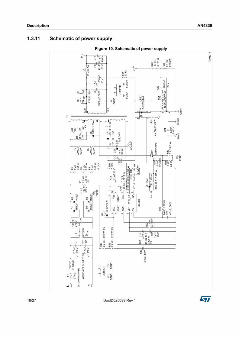
At startup, the L6564 device is powered by the VCC capacitor (C14), which is charged via resistors R3 and R9. As the capacitor C14 charges to turn on threshold of the L6564 device (typically at 12 V), the transformer T1 auxiliary winding (pins 5 - 6) generates the VCC voltage, rectified by the D7 and R12, that powers the L6564 during normal operation. The R11 is also connected to the auxiliary winding to provide the transformer demagnetization signal to the L6564 ZCD pin, turning on the MOSFET at any switching cycle. The MOSFET used is the STP4N80K5, a standard, low cost 800 V device housed in a TO-220 package, and needing only a small heatsink. The transformer is layer type, using a standard ferrite size EF25. The flyback reflected voltage is close to 170 V, providing enough room for the leakage inductance voltage spike still within the reliability margin of the MOSFET even at 300 VAC input.
The RCD snubber circuit using the R4, C5 and D6 clamps the peak of the leakage inductance voltage spike at the MOSFET turn-off. The resistor R2 is usually inserted in series with a subbing capacitor C5 to kill the spike and reduces further the EMI generated due to leakage spikes. The resistors R31 and R32 sense the current flowing into the transformer primary side. Once the signal at the current sense pin has reached the level programmed by the internal multiplier of the L6564, the MOSFET turns off. The divider R7, R10, R13 and R21 provides to the L6564 multiplier pin with instantaneous voltage information which is used to modulate the current flowing into the transformer primary side. The C16 is a small noise suppression capacitor, of course the purpose of this capacitor is not to disturb the actual sinusoidal mains information.
The output regulation is done by means of an isolated voltage loop by the optocoupler U2, and using an inexpensive TL431 device to drive the optocoupler. The opto-transistor modulates the input voltage of the L6564 internal amplifier, thus closing the voltage loop. The output rectifier is a Schottky rectifier, selected according to its maximum reverse voltage, forward voltage drop and power dissipation. A small LC filter is added on the output, filtering the high frequency ripple.
1.3.1 PFC_OK
PFC_OK function in PFC operation
PFC pre-regulator output voltage monitoring/disable function
This pin senses the output voltage of the PFC pre-regulator through a resistor divider and is used for protection purposes. If the voltage on the pin exceeds 2.5 V the IC stops switching and restarts as the voltage on the pin falls below 2.4 V. However, if the voltage of the INV pin falls 40 mV below that of the pin PFC_OK, a feedback failure is assumed. In this case the device is latched off. Normal operation can be resumed only by cycling VCC, bringing its value lower than 6 V before to move up to turn on threshold. If the voltage on this pin is brought below 0.23 V the IC is shut down. To restart the IC the voltage on the pin must go above 0.27 V. This can also be used as a remote on/off control input. Refer to Figure 3: PFC_OK function in PFC operation, the R3 and R4 composes the network to activate PFC output overvoltage shutdown.

Description AN4339
6/27 DocID025039 Rev 1
Figure 3. PFC_OK function in PFC operation
PFC_OK function in flyback operation
The same pin can also be used in case of flyback converter to shutdown the converter either in case of input overvoltage or output overvoltage. For input overvoltage protection, the pin one can be biased using the resistor divider network at rectified DC voltage to activate input overvoltage protection at the required mains OVP level. Referring to the circuit portion below, R3, R4 composes the network to activate mains overvoltage shutdown, where small capacitor C2 is used to average the DC value of sensing voltage at the PFC_OK pin. In the schematic in Figure 10 on page 18 the biasing components R1, R6, R8 and R19 comprises the input OVP detection circuit. The divider ratio is selected to provide 2.5 V at required mains OVP level.
If output overvoltage protection is preferred instead of mains OVP, we can utilize the auxiliary winding output, which is used to provide the operating voltage to the controller as well as demagnetization input to ZCD. Since we get the reflection of output voltage at auxiliary output supply so we can simply tap the signal for PFC_OK which is programmed to 2.5 V using resistor divider network at desired output OVP. This is achieved using the resistor divider network R4 and R5 at auxiliary output supply in Figure 4. In our circuit we have implemented input OVP protection network to bias PFC_OK. So the R14 in the schematic is kept open.

DocID025039 Rev 1 7/27
AN4339 Description
27
Figure 4. PFC_OK function in flyback operation
1.3.2 VFF (feed-forward function) and brownout protection
This is second input to the multiplier block for 1/V2 function. A capacitor and a parallel resistor must be connected from this pin to GND. They complete the internal peak-holding circuit that derives the information on the RMS mains voltage. The voltage at this pin, a DC level equal to the peak voltage on the pin MULT (pin 3), compensates the control loop gain dependence on the mains voltage. The variation of internal current reference signal VCSX versus the mains voltage level detected at MULT input (VFF = VMULT) is shown in the graph in Figure 5. This is the ultimate signal which is compared with the error signal to output the required gate signal ON time. Never connect the pin directly to GND but with a resistor ranging from 100 K (minimum) to 2 M (maximum). This pin is internally connected to a comparator in order to provide brownout (AC mains undervoltage) protection. A voltage below 0.8 V shuts down (not latched) the IC and brings its consumption to a considerably lower level. The IC restarts as the voltage at this pin goes above 0.88 V.
This is one of the important features of the L6564 device where we can manage the overload condition and it prevents excessive current to flow through the input section at worst low mains operating condition. So as the mains voltage drops below a programmed level, the IC stops as VFF pin detects the brownout level.

Description AN4339
8/27 DocID025039 Rev 1
Figure 5. VFF pin
1.3.3 Power supply basic specifications
Table 1. SMPS basic specifications
Parameters Limits
Rated input voltage range 90 - 265 VAC
Operating input voltage range 90 - 280 VAC
Input overvoltage shutdown > 280 VAC
Input supply frequency (fL) 47 - 63 Hz
Input / output isolation Yes, > 2.7 KV
Power factor correction Yes, > 0.9
THD As per IEC61000-3-2
Nominal output voltage 24 V+/-1 V
Load current 1 A
Total output power 24 W
Efficiency (full load for wide mains variations) > 85%
Output voltage pk-pk ripple (2.fL) < 20%
Topology Single stage HPF flyback
Maximum ambient temperature 45 °C

DocID025039 Rev 1 9/27
AN4339 Description
27
1.3.4 Calculations
Min. AC input, Vacmin = 90 VAC
Max. AC input, Vacmax = 265 VAC
Output DC voltage, VOUT = 24 VDC
Load current, IOUT = 1 A
Overall efficiency, = 0.87
Output voltage 2fL ripple = 2 Vpk-pk
Reflected voltage, VOR = 170 V
Minimum switching frequency, fswmin = 40 KHz
Min. DC voltage:
Equation 1
Vpkmin = 2.Vacmin - Vdson
Vpkmin = 123 V (taking Vdson = 4 V)
Max. DC voltage:
Equation 2
Vpkmax = 2.Vacmax - Vdson
Vpkmax = 370 V
Input power:
Equation 3
PIN = POUT/
PIN = 27.6 W
Peak to reflected voltage:
Equation 4
Kv = Vpkmin/VR
Kv = 0.723
Flyback characteristic functions are:
Equation 5
F1(Kv) = 0.42
Equation 6
F2(Kv) = 0.315
F1 Kv 0.637 4.6 103– Kv+
1 0.729 Kv+------------------------------------------------------------=
F2 Kv 0.5 1.4 103– Kv+
1 0.815 Kv+------------------------------------------------------=

Description AN4339
10/27 DocID025039 Rev 1
Equation 7
F3 (Kv) = 0.26
Peak primary current:
Equation 8
Ipkp = 1.42 A
RMS primary current:
Equation 9
Irmsp = 0.46 A
Peak secondary current:
Equation 10
Ipks = 8.8 A
RMS secondary current:
Equation 11
Irsms = 2.2 A
F3 Kv 0.424 5.7 104– Kv+
1 0.862 Kv+------------------------------------------------------------=
Ipkp2 pin
Vpkmin F2 Kv -----------------------------------------------=
Irmsp Ipkp F2 Kv 3
-------------------=
Ipks2 Iout
Kv F2 Kv ---------------------------------=
Irmss Ipks Kv F3 Kv 3
---------------------------------=
DocID025039 Rev 1 11/27
AN4339 Description
27
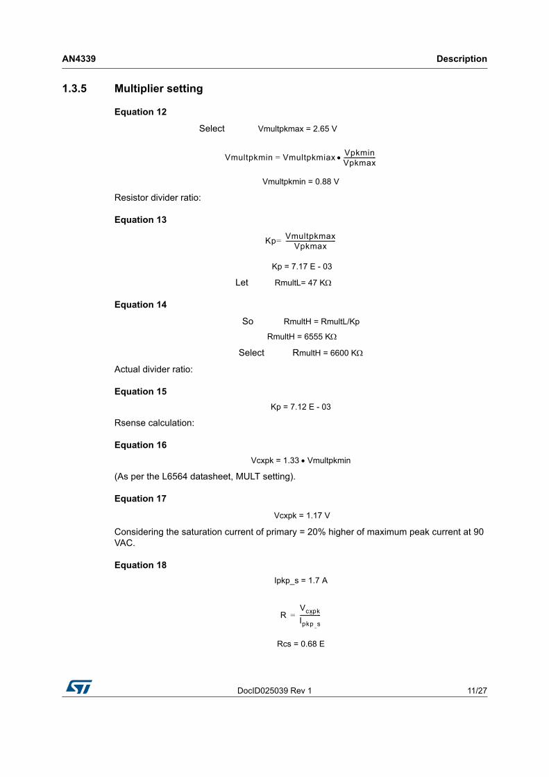
1.3.5 Multiplier setting
Equation 12
Select Vmultpkmax = 2.65 V
Vmultpkmin = 0.88 V
Resistor divider ratio:
Equation 13
Kp = 7.17 E - 03
Let RmultL= 47 K
Equation 14
So RmultH = RmultL/Kp
RmultH = 6555 K
Select RmultH = 6600 K
Actual divider ratio:
Equation 15
Kp = 7.12 E - 03
Rsense calculation:
Equation 16
Vcxpk = 1.33 Vmultpkmin
(As per the L6564 datasheet, MULT setting).
Equation 17
Vcxpk = 1.17 V
Considering the saturation current of primary = 20% higher of maximum peak current at 90 VAC.
Equation 18
Ipkp_s = 1.7 A
Rcs = 0.68 E
Vmultpkmin VmultpkmiaxVpkminVpkmax-----------------------=
KpVmultpkmax
Vpkmax------------------------------------=
RVcxpk
Ipkp s---------------=

Description AN4339
12/27 DocID025039 Rev 1
1.3.6 Transformer design
Primary inductance value is calculated by Equation 19:
Equation 19
Lp = 1.25 mH
Select Lp = 1 mH
Primary to secondary turn ratio:
Equation 20
n = 6.911
Primary number of turns:
Equation 21
Considering max flux density:
Bmax = 0.3 T
Select core EE25 (After calculating the minimum area product required, not described in this section).
Cross sectional area:
Equation 22
Ae = 0.52 cm2
Primary number of turns:
Equation 23
Np = 91
Select Np = 90 T
Secondary number of turns:
Equation 24
Ns = Np/n
Ns = 13 T
Aux. voltage required: Vaux = 15 V
Lp
Vpkmin 103
1 Kv+ fswmin Ipkp------------------------------------------------------------------=
nVor
VOUT VF+-----------------------------=
Np
Lp 103–
Ipkp
Bmax Ae 104–
--------------------------------------------=

DocID025039 Rev 1 13/27
AN4339 Description
27
Number of turns required for auxiliary winding:
Equation 25
Naux = 8 T
1.3.7 Control loop design
The error amplifier block is shown in Figure 6:
Figure 6. Error amplifier block
Error amplifier transfer function is:
Equation 26
Naux
Vaux NsVout
-------------------------=
G1 s R15–R18--------------
1
s1---
C12 R16----------------------------+
1
s1---
C12 R15 R16+ ---------------------------------------------------+
------------------------------------------------------------------=

Description AN4339
14/27 DocID025039 Rev 1
Poles and zero from error amplifier transfer function are:
Equation 27
Transfer function of feedback loop is:
Equation 28
Where CTRmin = 0.5 - minimum current transfer ratio of optocoupler in feedback loop.
Poles and zero of above transfer function are:
Equation 29
Selecting R15 = 47 K, R26 = 47 K, R28 = 4.7 K, C19 = 1 F, C12 = 22 nF; the open loop cross over frequency is 13 Hz and desired phase margin is 40°.
fz11
2 C12 R16----------------------------------------------=
fp11
2 C12 R15 R16+ ---------------------------------------------------------------------=
H s 1R27----------- R18 R24
R18 R24+----------------------------- CTRmin
1
s1---
C19 R28 R26+ ---------------------------------------------------+
s1---
R26 C19----------------------------
------------------------------------------------------------------=
fp21
2 R26 C19----------------------------------------------=
fz21
2 C19 R28 R26+ ---------------------------------------------------------------------=

DocID025039 Rev 1 15/27
AN4339 Description
27
Figure 7. Open loop overall transfer function
Figure 8. Phase

Description AN4339
16/27 DocID025039 Rev 1
1.3.8 Transformer specification
Table 2. Transformer specification
1.3.9 Winding details
Max. output power Max. 28 W (typ. operating power is 24 W)
Input voltage range 90 - 280 VAC
Primary inductance 1.0 ± 0.1 mH at 50 KHz
Primary side leakage inductance < 3 H at 50 KHz
Peak primary current 1.42 A
Saturation current 1.8 A
RMS primary current 0.46 A
Peak secondary current 8.8 A
RMS secondary current 2.2 A
Minimum switching frequency 40 KHz
Core size E25/13/7
Ferrite material N87, EPCOS
Bobbin 12 pins horizontal
Dielectric strength > 2.7 KV
Table 3. Winding details
Winding name Start Stop No. of turns Wire gauge Order of windings
Np1 3 2 45 3 x 0.25 mm Bottom
Naux 5 6 8 1 x 0.15 mm Above Np1
Nsec 12, 11 10, 9 13 6 x 0.25 mm Above Naux
Np2 2 1 45 3 x 0.25 mm Topmost

DocID025039 Rev 1 17/27
AN4339 Description
27
1.3.10 Transformer construction
Figure 9. Transformer construction
Description AN4339
18/27 DocID025039 Rev 1
1.3.11 Schematic of power supply
Figure 10. Schematic of power supply

DocID025039 Rev 1 19/27
AN4339 Description
27
1.4 BLDC motor driver - L6235 details
Motor specifications are
3-phase BLDC motor
DC input voltage: 24 V
Typical operating current: 1 A
3 Hall sensor detection method
To drive the BLDC motor with Hall effect sensors incorporated, the L6235 device is used. The L6235 device is a DMOS fully integrated 3-phase motor driver with overcurrent protection. The device combines isolated DMOS power transistors with CMOS and bipolar circuits on the same chip. The device includes all the circuitry needed to drive a 3-phase BLDC motor including: a 3-phase DMOS bridge, a constant off time PWM current controller and the decoding logic for single ended Hall sensors that generates the required sequence for the power stage. The L6235 device features a non-dissipative overcurrent protection on the high side Power MOSFETs and thermal shutdown. Some of the important features of the driver are listed below:
Operating supply voltage from 8 to 52 V
5.6 A output peak current (2.8 ADC)
Rds(on) 0.3 W typ. value at TJ = 25 °C
Operating frequency up to 100 KHz
Non dissipative overcurrent, detection and protection
Diagnostic output
Constant TOFF PWM current controller
Slow decay synchronous. rectification
60° and 120° Hall effect decoding logic
Brake function
TACHO output for speed loop
Cross conduction protection
Thermal shutdown
Undervoltage lockout
Integrated fast freewheeling diodes

Description AN4339
20/27 DocID025039 Rev 1
1.4.1 L6235 block diagram
Figure 11. L6235 block diagram
The detail description of some of the pins of driver is given in Section 1.4.2 to Section 1.4.10.
1.4.2 SENSEA and SENSEB
These are half bridge sections source pins. SENSEA and SENSEB pins have to be connected together and to power ground through a sensing power resistor. At the pin SENSEB, the inverted pin of an internal sense comparator is connected.
1.4.3 Hall sensors inputs (H1, H2, and H3)
These are Hall sensor inputs to controller to detect the position of motor. We need pull-up resistors connected at these pins to connect the Hall sensors inputs.

DocID025039 Rev 1 21/27
AN4339 Description
27
1.4.4 TACHO
It allows developing an easy speed control loop by using an external op-amp. This is an open drain output. At each rising edge of the Hall effect sensors H1, the monostable is triggered and the MOSFET connected to the pin TACHO is turned off for a constant time tPULSE (as shown in Figure 12). The off time tPULSE can be set using the external RC network (RPUL, CPUL) connected to the pin RCPULSE. Figure 12 gives the relation between tPULSE and CPUL, RPUL. We have approximately:
Equation 30
tPULSE = 0.6 · RPUL · CPUL
Figure 12. tPULSE versus CPUL and RPUL
Where CPUL should be chosen in the range of 1 nF to 100 nF and RPUL in the range of 20 K to 100 K. By connecting the tachometer pin to an external pull-up resistor, the output signal average value VM is proportional to the frequency of the Hall effect signal and, therefore, to the motor speed. This realizes a simple frequency-to-voltage converter. An op-amp, configured as an integrator, filters the signal and compares it with a reference voltage VREF, which sets the speed of the motor. So we can also connect the non-inverting pin of op-amp by using a potentiometer at VREF pin to vary the speed of motor.
Equation 31
VM
tPULSE
T------------------ VDD=

Description AN4339
22/27 DocID025039 Rev 1
1.4.5 Typical TACHO waveforms and speed control loop
Figure 13. Typical TACHO waveforms and speed control loop
1.4.6 BRAKE function
Brake input pin. Low logic level switches on all high side Power MOSFETs, implementing the brake function. If not used, it has to be connected to +5 V.
1.4.7 FWD/REV functions
Input to forward and reverse function for the motor i.e to select the direction of the rotation. HIGH logic level sets forward operation, whereas LOW logic level sets reverse operation. If not used, it has to be connected to GND or +5 V.
1.4.8 Enable input (EN)
Chip enable input. LOW logic level switches OFF all Power MOSFETs. If not used, it has to be connected to +5 V.
1.4.9 RCPULSE
RC network pin. A parallel RC network connected between this pin and ground sets the duration of the monostable pulse used for the frequency-to-voltage converter.
1.4.10 RCOFF
An external parallel RC network is connected to the RCOFF to set the current controller off time.

DocID025039 Rev 1 23/27
AN4339 Description
27
1.4.11 Schematic of motor driving section
Figure 14. Schematic of motor driving section

Description AN4339
24/27 DocID025039 Rev 1
1.4.12 Hall sensors
Following bipolar type Hall sensors can be used for this application:
Part no: US2881
Manufacturer: Melexis
Figure 15. Typical application schematic
Figure 16. SE and UA package
Table 4. Pin descriptions
SE pin no. UA pin no. Name Type Function
1 1 VDD Supply Supply voltage pin
2 3 OUT Output Open drain output pin
3 2 GND Ground Ground pin

DocID025039 Rev 1 25/27
AN4339 Description
27
Table 5. Bill of material (ST parts only)
Part description Quantity
PFC controller, L6564D 1
MOSFET, STP4N80K5 1
Rectifier STPS3150U 1
Rectifier STTH1L06A 1
3-phase BLDC driver, L6235PD 1
Operational amplifier, LM358 1

References AN4339
26/27 DocID025039 Rev 1
2 References
1. AN1059: Design equations of high-power-factor flyback converters based on the L6561.
2. L6564 datasheet: 10 pin transition-mode PFC controller.
3. L6235 datasheet: DMOS driver for three-phase brushless DC motor.
4. EVAL6235PD databrief.
3 Revision history
Table 6. Document revision history
Date Revision Changes
29-Nov-2013 1 Initial release.

DocID025039 Rev 1 27/27
AN4339
27
Please Read Carefully:
Information in this document is provided solely in connection with ST products. STMicroelectronics NV and its subsidiaries (“ST”) reserve theright to make changes, corrections, modifications or improvements, to this document, and the products and services described herein at anytime, without notice.
All ST products are sold pursuant to ST’s terms and conditions of sale.
Purchasers are solely responsible for the choice, selection and use of the ST products and services described herein, and ST assumes noliability whatsoever relating to the choice, selection or use of the ST products and services described herein.
No license, express or implied, by estoppel or otherwise, to any intellectual property rights is granted under this document. If any part of thisdocument refers to any third party products or services it shall not be deemed a license grant by ST for the use of such third party productsor services, or any intellectual property contained therein or considered as a warranty covering the use in any manner whatsoever of suchthird party products or services or any intellectual property contained therein.
UNLESS OTHERWISE SET FORTH IN ST’S TERMS AND CONDITIONS OF SALE ST DISCLAIMS ANY EXPRESS OR IMPLIEDWARRANTY WITH RESPECT TO THE USE AND/OR SALE OF ST PRODUCTS INCLUDING WITHOUT LIMITATION IMPLIEDWARRANTIES OF MERCHANTABILITY, FITNESS FOR A PARTICULAR PURPOSE (AND THEIR EQUIVALENTS UNDER THE LAWSOF ANY JURISDICTION), OR INFRINGEMENT OF ANY PATENT, COPYRIGHT OR OTHER INTELLECTUAL PROPERTY RIGHT.
ST PRODUCTS ARE NOT DESIGNED OR AUTHORIZED FOR USE IN: (A) SAFETY CRITICAL APPLICATIONS SUCH AS LIFESUPPORTING, ACTIVE IMPLANTED DEVICES OR SYSTEMS WITH PRODUCT FUNCTIONAL SAFETY REQUIREMENTS; (B)AERONAUTIC APPLICATIONS; (C) AUTOMOTIVE APPLICATIONS OR ENVIRONMENTS, AND/OR (D) AEROSPACE APPLICATIONSOR ENVIRONMENTS. WHERE ST PRODUCTS ARE NOT DESIGNED FOR SUCH USE, THE PURCHASER SHALL USE PRODUCTS ATPURCHASER’S SOLE RISK, EVEN IF ST HAS BEEN INFORMED IN WRITING OF SUCH USAGE, UNLESS A PRODUCT ISEXPRESSLY DESIGNATED BY ST AS BEING INTENDED FOR “AUTOMOTIVE, AUTOMOTIVE SAFETY OR MEDICAL” INDUSTRYDOMAINS ACCORDING TO ST PRODUCT DESIGN SPECIFICATIONS. PRODUCTS FORMALLY ESCC, QML OR JAN QUALIFIED AREDEEMED SUITABLE FOR USE IN AEROSPACE BY THE CORRESPONDING GOVERNMENTAL AGENCY.
Resale of ST products with provisions different from the statements and/or technical features set forth in this document shall immediately voidany warranty granted by ST for the ST product or service described herein and shall not create or extend in any manner whatsoever, anyliability of ST.
ST and the ST logo are trademarks or registered trademarks of ST in various countries.Information in this document supersedes and replaces all information previously supplied.
The ST logo is a registered trademark of STMicroelectronics. All other names are the property of their respective owners.
© 2013 STMicroelectronics - All rights reserved
STMicroelectronics group of companies
Australia - Belgium - Brazil - Canada - China - Czech Republic - Finland - France - Germany - Hong Kong - India - Israel - Italy - Japan - Malaysia - Malta - Morocco - Philippines - Singapore - Spain - Sweden - Switzerland - United Kingdom - United States of America
www.st.com