Embed Size (px)
Citation preview

August 2011 Doc ID 018857 Rev 1 1/25
AN3407Application note
Resonant driver for LED SMPS demonstration boardbased on the L6585DE
IntroductionThis application note describes the performance of a 100 W LED switched-mode power supply (SMPS). The L6585DE embeds a high-performance transition mode (TM) power factor correction (PFC) controller, half-bridge (HB) controller and all the relevant drivers necessary to build a combo IC. The L6585DE embeds a wide range of features to provide an energy-saving and cost-effective solution for the LED SMPS demonstration board (STEVAL-ILL038V1).
Previous dedicated ICs for LED SMPS applications allowed designers to achieve good driver efficiency. The PFC section has superior performance in terms of harmonic content mitigation. High power factor (PF) and total harmonic distortion (THD) reduction are obtained as required by international norms, especially concerning universal input voltage operations. The TM PFC operation and high-efficiency performance of the half-bridge topology provide very good overall circuit efficiency.
Film capacitors are one of the most popular types of discrete components. They generally offer excellent electrical properties and are advantageous in high current and high temperature conditions. For these reasons, film capacitors are used in LED SMPS applications. In order to guarantee maintenance-free operation required by these types of applications during the useful lifetime of the LED, electrolytic capacitors have been replaced by film capacitors in the STEVAL-ILL038V1 board.
Other features, such as half-bridge overcurrent with frequency increase and PFC overvoltage, allow designers to build a reliable, flexible solution with a reduced component count.
Figure 1. STEVAL-ILL038V1 demonstration board
www.st.com

Contents AN3407
2/25 Doc ID 018857 Rev 1
Contents
1 L6585DE combo IC . . . . . . . . . . . . . . . . . . . . . . . . . . . . . . . . . . . . . . . . . . 4
2 Main characteristics and circuit description . . . . . . . . . . . . . . . . . . . . . 5
2.1 VCC section . . . . . . . . . . . . . . . . . . . . . . . . . . . . . . . . . . . . . . . . . . . . . . . . 5
2.2 Power factor corrector section . . . . . . . . . . . . . . . . . . . . . . . . . . . . . . . . . . 5
2.3 Resonant power section . . . . . . . . . . . . . . . . . . . . . . . . . . . . . . . . . . . . . . . 6
2.4 Output voltage feedback loop . . . . . . . . . . . . . . . . . . . . . . . . . . . . . . . . . . . 7
3 Efficiency measurements . . . . . . . . . . . . . . . . . . . . . . . . . . . . . . . . . . . . . 9
4 Input current harmonics measurement . . . . . . . . . . . . . . . . . . . . . . . . . 11
5 Functional check . . . . . . . . . . . . . . . . . . . . . . . . . . . . . . . . . . . . . . . . . . . 13
5.1 PFC circuit . . . . . . . . . . . . . . . . . . . . . . . . . . . . . . . . . . . . . . . . . . . . . . . . 13
5.2 Half-bridge resonant LLC circuit . . . . . . . . . . . . . . . . . . . . . . . . . . . . . . . . 14
5.3 Converter startup . . . . . . . . . . . . . . . . . . . . . . . . . . . . . . . . . . . . . . . . . . . 15
6 Bill of material . . . . . . . . . . . . . . . . . . . . . . . . . . . . . . . . . . . . . . . . . . . . . 16
7 EMI choke . . . . . . . . . . . . . . . . . . . . . . . . . . . . . . . . . . . . . . . . . . . . . . . . . 20
8 PFC coil specifications . . . . . . . . . . . . . . . . . . . . . . . . . . . . . . . . . . . . . . 21
9 Transformer specifications . . . . . . . . . . . . . . . . . . . . . . . . . . . . . . . . . . 22
10 References . . . . . . . . . . . . . . . . . . . . . . . . . . . . . . . . . . . . . . . . . . . . . . . 23
11 Revision history . . . . . . . . . . . . . . . . . . . . . . . . . . . . . . . . . . . . . . . . . . . 24

AN3407 List of figures
Doc ID 018857 Rev 1 3/25
List of figures
Figure 1. STEVAL-ILL038V1 demonstration board . . . . . . . . . . . . . . . . . . . . . . . . . . . . . . . . . . . . . . . 1Figure 2. Application example . . . . . . . . . . . . . . . . . . . . . . . . . . . . . . . . . . . . . . . . . . . . . . . . . . . . . . . 4Figure 3. Multiplier . . . . . . . . . . . . . . . . . . . . . . . . . . . . . . . . . . . . . . . . . . . . . . . . . . . . . . . . . . . . . . . . 6Figure 4. Oscillator characteristics . . . . . . . . . . . . . . . . . . . . . . . . . . . . . . . . . . . . . . . . . . . . . . . . . . . . 7Figure 5. Half-bridge protection thresholds during run mode. . . . . . . . . . . . . . . . . . . . . . . . . . . . . . . . 7Figure 6. Electrical schematic . . . . . . . . . . . . . . . . . . . . . . . . . . . . . . . . . . . . . . . . . . . . . . . . . . . . . . . 8Figure 7. STEVAL-ILL038V1 demonstration board: efficiency vs. load . . . . . . . . . . . . . . . . . . . . . . . 10Figure 8. STEVAL-ILL038V1 demonstration board: full-load efficiency vs. VAC. . . . . . . . . . . . . . . . 10Figure 9. STEVAL-ILL038V1 demonstration board: power factor vs. load . . . . . . . . . . . . . . . . . . . . 10Figure 10. EN61000-3-2 Class-D standard - 185 VAC/50 Hz, THD=4.86%, PF=0.993 at full load. . . 11Figure 11. EN61000-3-2 Class-D standard - 230 VAC/50 Hz, THD=5.98%, PF=0.980 at full load. . . 11Figure 12. Input current waveforms - full load at 115 VAC . . . . . . . . . . . . . . . . . . . . . . . . . . . . . . . . . 12Figure 13. Input current waveforms - full load at 230 VAC . . . . . . . . . . . . . . . . . . . . . . . . . . . . . . . . . 12Figure 14. PFC stage waveforms at 115 VAC - full load . . . . . . . . . . . . . . . . . . . . . . . . . . . . . . . . . . . 13Figure 15. PFC stage waveforms at 230 VAC - full load . . . . . . . . . . . . . . . . . . . . . . . . . . . . . . . . . . . 13Figure 16. PFC stage waveforms at 115 VAC - full load - detail . . . . . . . . . . . . . . . . . . . . . . . . . . . . . 13Figure 17. PFC stage waveforms at 230 VAC - full load - detail . . . . . . . . . . . . . . . . . . . . . . . . . . . . . 13Figure 18. Primary side LLC waveforms at 115 VAC - full load . . . . . . . . . . . . . . . . . . . . . . . . . . . . 14Figure 19. Secondary side LLC waveforms at 230 VAC - full load . . . . . . . . . . . . . . . . . . . . . . . . . . . 14Figure 20. High-frequency ripple on output voltage at 115 VAC - 60 Hz - full load . . . . . . . . . . . . . . . 15Figure 21. Low-frequency ripple on output voltage at 115 VAC - 60 Hz - full load . . . . . . . . . . . . . . . 15Figure 22. Wake-up at 115 VAC - 60 Hz - full load . . . . . . . . . . . . . . . . . . . . . . . . . . . . . . . . . . . . . . . 15Figure 23. Wake-up at 230 VAC - 60 Hz - full load . . . . . . . . . . . . . . . . . . . . . . . . . . . . . . . . . . . . . . . 15Figure 24. PCB: topside and through-hole components . . . . . . . . . . . . . . . . . . . . . . . . . . . . . . . . . . . 18Figure 25. PCB: bottomside and SMD components . . . . . . . . . . . . . . . . . . . . . . . . . . . . . . . . . . . . . . 18Figure 26. PCB: topside placement . . . . . . . . . . . . . . . . . . . . . . . . . . . . . . . . . . . . . . . . . . . . . . . . . . . 19Figure 27. PCB: bottomside placement . . . . . . . . . . . . . . . . . . . . . . . . . . . . . . . . . . . . . . . . . . . . . . . . 19Figure 28. EMI: OTC21V-4S vertical type EMI choke . . . . . . . . . . . . . . . . . . . . . . . . . . . . . . . . . . . . . 20Figure 29. PFC: QP2520V-vertical type for PFC choke. . . . . . . . . . . . . . . . . . . . . . . . . . . . . . . . . . . . 21Figure 30. Transformer: LP2920H - horizontal type for LLC transformer. . . . . . . . . . . . . . . . . . . . . . . 22

L6585DE combo IC AN3407
4/25 Doc ID 018857 Rev 1
1 L6585DE combo IC
The L6585DE embeds both a PFC converter and a half-bridge resonant in a single SO20 package.
● Transition mode PFC converter with overvoltage and overcurrent protection
● Half-bridge controller with high-voltage driver (600 Vdc) and integrated bootstrap diode
● 3% precise, fully programmable oscillator
● Overcurrent protection
● Hard-switching detection
Figure 2. Application example

AN3407 Main characteristics and circuit description
Doc ID 018857 Rev 1 5/25
2 Main characteristics and circuit description
The main features of the SMPS are listed here below:
● Extended input mains range: 90 ~ 265 VAC - frequency 50/60 Hz
● Output voltage: 48 V at 2.08 A
● Long-life, electrolytic capacitors are not used
● Mains harmonics: according to EN61000-3-2 Class-D
● Efficiency at full load: better than 90%
● Dimensions: 75 x 135 mm
2.1 VCC sectionThe L6585DE is supplied by applying voltage between the VCC pin and GND pin. An undervoltage lockout (UVLO) prevents the IC from operating with supply voltages too low to guarantee the correct behavior of the internal structures.
An internal voltage clamp limits the voltage to around 17 V and a delivery up to 20 mA. For this reason it cannot be used directly as a clamp for the charge pump (current peaks usually reach several hundreds of mA), but can be easily used during startup in order to charge the VCC capacitor or during save mode in order to keep the IC alive, for example, connecting VCC to input voltage through a resistor.
The L6585DE is supplied by the startup MOSFET Q4 and R40 charging the capacitor C25. A charge pump connected to the auxiliary winding of the HB inductor T2 supplies the controller via a small linear regulator represented by Q7. Once both stages have been activated, the controllers are supplied also by the auxiliary winding of the resonant transformer, assuring correct supply voltage during all load conditions. As the voltage on the VCC pin reaches the turn-on threshold, the chip is enabled, and the half-bridge and the PFC sections start at the same time.
2.2 Power factor corrector sectionThe PFC output voltage is controlled by means of a voltage-mode error amplifier and a precise internal voltage reference. The PFC section achieves current mode control operating in transition mode, offering a highly linear multiplier including a THD optimizer that allows for an extremely low THD, even over a large range of input voltages and loading conditions.
The controller is the L6585DE (U1), working in transition mode and integrating all functions that are needed to perform the PFC. It delivers a stable 450 Vdc. It is a conventional boost converter connected to the output of the rectifier bridge. It includes the coil T1, the PFC transformer by YuJing, the diode D2 (STTH3L06U) and the PFC output capacitors C2, C3 and C4 by film type of 5 µF/800 V. The T1 provides also the information about the PFC coil core demagnetization to pin#11 (ZCD) of the L6585DE. The T1 auxiliary winding is connected to pin#11 (ZCD) of the L6585DE through the resistor R10. Its purpose is to provide the information that T1 has demagnetized which is needed by the internal logic for triggering a new switching cycle. The boost switch is represented by the power MOSFET Q2. The T1 secondary winding (pins#8-6) and related circuitry are dedicated to power the L6585DE during normal operation.
Main characteristics and circuit description AN3407
6/25 Doc ID 018857 Rev 1
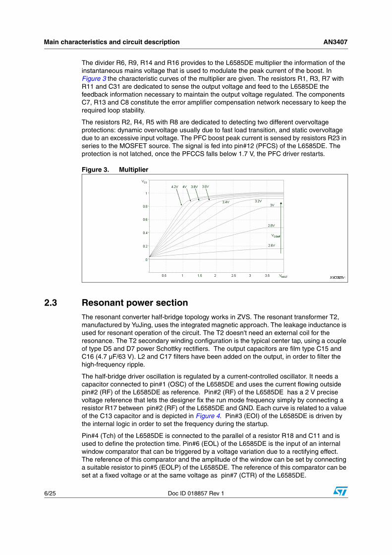
The divider R6, R9, R14 and R16 provides to the L6585DE multiplier the information of the instantaneous mains voltage that is used to modulate the peak current of the boost. In Figure 3 the characteristic curves of the multiplier are given. The resistors R1, R3, R7 with R11 and C31 are dedicated to sense the output voltage and feed to the L6585DE the feedback information necessary to maintain the output voltage regulated. The components C7, R13 and C8 constitute the error amplifier compensation network necessary to keep the required loop stability.
The resistors R2, R4, R5 with R8 are dedicated to detecting two different overvoltage protections: dynamic overvoltage usually due to fast load transition, and static overvoltage due to an excessive input voltage. The PFC boost peak current is sensed by resistors R23 in series to the MOSFET source. The signal is fed into pin#12 (PFCS) of the L6585DE. The protection is not latched, once the PFCCS falls below 1.7 V, the PFC driver restarts.
Figure 3. Multiplier
2.3 Resonant power sectionThe resonant converter half-bridge topology works in ZVS. The resonant transformer T2, manufactured by YuJing, uses the integrated magnetic approach. The leakage inductance is used for resonant operation of the circuit. The T2 doesn't need an external coil for the resonance. The T2 secondary winding configuration is the typical center tap, using a couple of type D5 and D7 power Schottky rectifiers. The output capacitors are film type C15 and C16 (4.7 µF/63 V). L2 and C17 filters have been added on the output, in order to filter the high-frequency ripple.
The half-bridge driver oscillation is regulated by a current-controlled oscillator. It needs a capacitor connected to pin#1 (OSC) of the L6585DE and uses the current flowing outside pin#2 (RF) of the L6585DE as reference. Pin#2 (RF) of the L6585DE has a 2 V precise voltage reference that lets the designer fix the run mode frequency simply by connecting a resistor R17 between pin#2 (RF) of the L6585DE and GND. Each curve is related to a value of the C13 capacitor and is depicted in Figure 4. Pin#3 (EOI) of the L6585DE is driven by the internal logic in order to set the frequency during the startup.
Pin#4 (Tch) of the L6585DE is connected to the parallel of a resistor R18 and C11 and is used to define the protection time. Pin#6 (EOL) of the L6585DE is the input of an internal window comparator that can be triggered by a voltage variation due to a rectifying effect. The reference of this comparator and the amplitude of the window can be set by connecting a suitable resistor to pin#5 (EOLP) of the L6585DE. The reference of this comparator can be set at a fixed voltage or at the same voltage as pin#7 (CTR) of the L6585DE.

AN3407 Main characteristics and circuit description
Doc ID 018857 Rev 1 7/25
Figure 4. Oscillator characteristics
Pin #14 (HBCS) of the L6585DE is equipped with a current sensing and a dedicated overcurrent management system. When the EOI voltage reaches 1.9 V, the IC enters run mode and the switching frequency is set only by R17 (RRUN). In Figure 5 the protection thresholds are shown. They are sensed by the circuit C18, R26, D8, D9, R27, and C19 and are fed into the L6585DE pin#14 (HBCS).
Figure 5. Half-bridge protection thresholds during run mode
2.4 Output voltage feedback loopThe output voltage is kept stable by means of a feedback loop implementing a typical circuit using U3 (TS2431) modulating the current in the optocoupler diode. On the primary side, R34 connecting pin#2 (RF) of the L6585DE to the optocoupler's phototransistor allows modulating the L6585DE oscillator frequency, thus keeping the output voltage regulated. R17 connects the same pin to ground and sets the minimum switching frequency.

Main characteristics and circuit description AN3407
8/25 Doc ID 018857 Rev 1
Figure 6. Electrical schematic

AN3407 Efficiency measurements
Doc ID 018857 Rev 1 9/25
3 Efficiency measurements
Table 1 shows the overall efficiency, measured at 115 VAC - 60 Hz. Table 2 shows the overall efficiency, measured at 230 VAC - 50 Hz.
The overall circuit efficiency is measured at different loads, powering the board at the two nominal input mains voltages. The measures have been done after 30 minutes at load. The high efficiency of the PFC working in transition mode and the very high efficiency of the resonant stage working in ZVS provides for an overall efficiency better than 90%.
Figure 7 shows the efficiency at 25%, 50%, 75% and 100% load at 115 VAC and 230 VAC. Figure 8 shows the efficiency at full load over the entire AC input voltage mains range. Figure 9 shows the power factor (PF) versus load variations.
Table 1. Efficiency at 115 VAC
Load115 VAC - 60 Hz
Vout (V) Iout (A) Pout (W) Pin (W) PF Eff (%)
25% 48.67 0.525 25.55 29.30 0.982 87.21
50% 48.67 1.050 51.10 55.87 0.996 91.47
75% 48.67 1.560 75.93 82.01 0.995 92.58
100% 48.67 2.086 101.53 109.28 0.991 92.90
Average eff. 91.04
Table 2. Efficiency at 230 VAC
Load230 VAC - 50Hz
Vout (V) Iout (A) Pout (W) Pin (W) PF Eff (%)
25% 48.67 0.525 25.55 29.45 0.793 86.76
50% 48.67 1.048 51.01 55.59 0.924 91.76
75% 48.67 1.560 75.93 81.06 0.966 93.67
100% 48.67 2.083 101.38 107.46 0.980 94.34
Average eff. 91.63

Efficiency measurements AN3407
10/25 Doc ID 018857 Rev 1
Figure 7. STEVAL-ILL038V1 demonstration board: efficiency vs. load
Figure 8. STEVAL-ILL038V1 demonstration board: full-load efficiency vs. VAC
Figure 9. STEVAL-ILL038V1 demonstration board: power factor vs. load

AN3407 Input current harmonics measurement
Doc ID 018857 Rev 1 11/25
4 Input current harmonics measurement
The internal THD optimizer increases the performance when the mains voltage reaches zero which reduces crossover distortion and avoids introducing offset. One of the main purposes of a PFC pre-conditioner is the correction of input current distortion, decreasing the harmonic contents below the limits of the relevant regulations. The board has been tested according to the European norm EN61000-3-2 Class-D, at full load and nominal input voltage mains. Figure 10 and 11 show the measurement results.
Figure 10. EN61000-3-2 Class-D standard - 185 VAC/50 Hz, THD=4.86%, PF=0.993 at full load
Figure 11. EN61000-3-2 Class-D standard - 230 VAC/50 Hz, THD=5.98%, PF=0.980 at full load

Input current harmonics measurement AN3407
12/25 Doc ID 018857 Rev 1
Figure 12 and 13 show the waveforms of the input current and voltage at 115 VAC and 230 VAC during full load.
Figure 12. Input current waveforms - full load at 115 VAC
Figure 13. Input current waveforms - full load at 230 VAC
CH2: Vac-in CH4: Iac-in CH2: Vac-in CH3: Iac-in

AN3407 Functional check
Doc ID 018857 Rev 1 13/25
5 Functional check
5.1 PFC circuitThe waveforms measured in the PFC stage have been captured during full load operation at nominal 115 VAC and 230 VAC in Figure 14 and 15. It can be seen in both figures that the envelope of the waveform of pin#12 (PFCS) is in phase with that of pin#8 (MULT) and has same sinusoidal shape, demonstrating the proper functionality of the PFC stage. It is also possible to measure the peak-to-peak value of the voltage ripple superimposed on the PFC output voltage due to the low value of the PFC output capacitors. The details of the waveforms at switching frequency are measured in Figure 16 and 17.
Figure 14. PFC stage waveforms at 115 VAC - full load
Figure 15. PFC stage waveforms at 230 VAC - full load
Figure 16. PFC stage waveforms at 115 VAC - full load - detail
Figure 17. PFC stage waveforms at 230 VAC - full load - detail
CH1: MULT CH4: Vout_PFCCH2: PFCS CH1: MULT CH4: Vout_PFCCH2: PFCS
CH1: MULT CH3: Vout_PFCCH3: Vdrain_Q2 CH1: MULT CH4: Vout_PFCCH3: Vdrain_Q2

Functional check AN3407
14/25 Doc ID 018857 Rev 1
5.2 Half-bridge resonant LLC circuitThe waveforms are measured in the resonant stage ZVS operation in Figure 18. Both MOSFETs are turned on when resonant current is flowing through their body diodes and drain-source voltage is almost zero, thus achieving good efficiency. The switching frequency has been chosen around 94 kHz.
Figure 18 shows waveforms during steady-state operation of the circuit at full load. A slight asymmetry of operating modes by each half portion of the sine wave is visible: one half-cycle is working at resonant frequency while the other half is working above the resonant frequency. This is due to a small difference between each half’s secondary leakage inductance of the transformer reflected to the primary side, providing two slightly different resonant frequencies. This phenomenon is typically due to a different coupling of the transformer’s secondary windings and in this case it is not an issue.
Figure 19 demonstrates that during one half-cycle the circuit is working below the resonant frequency, while during the following half-cycle it is working at resonance frequency. Waveforms relevant to the secondary side are shown: the rectifier’s reverse voltage is measured by Ch3 and Ch4 on the right of the picture. It is a bit higher than the theoretical value that would be 2 (VOUT+VF), hence about 100 V.
Figure 18. Primary side LLC waveforms at 115 VAC - full load
Figure 19. Secondary side LLC waveforms at 230 VAC - full load
CH1: VCC CH4: HBCH3: Res. Tank current CH1: Vout CH4: V_D5CH3: V_D7

AN3407 Functional check
Doc ID 018857 Rev 1 15/25
The ripple and noise on the output voltage is shown on CH1. Figure 20 shows the waveform during the high-frequency ripple of the circuit at full load. The peak-to-peak value is high but it doesn't affect the application, in fact the converters regulating the current flowing in each LED strip can reject the ripple. Figure 21 shows the waveform during the low-frequency ripple of the circuit at full load.
5.3 Converter startupThe converter startup is captured in Figure 22 and 23. The converter begins operation around 80 ms at 115 VAC and 230 VAC. This is the time needed to charge the VCC to turn-on voltage. The L6585DE starts switching and the PFC and HB output voltage starts increasing.
Figure 20. High-frequency ripple on output voltage at 115 VAC - 60 Hz - full load
Figure 21. Low-frequency ripple on output voltage at 115 VAC - 60 Hz - full load
CH1: Vout CH1: Vout
Figure 22. Wake-up at 115 VAC - 60 Hz - full load
Figure 23. Wake-up at 230 VAC - 60 Hz - full load
CH1: VCC CH3: VOUT CH4: HB CH1: VCC CH3: VOUT CH4: HB

Bill of material AN3407
16/25 Doc ID 018857 Rev 1
6 Bill of material
Table 3. STEVAL-ILL038V1 demonstration board: bill of material
Reference Part / value Tolerance % Voltage Manufacturer
BD1 GBU8J_DIP VISHAY
C1,C5,C9 470nF_DIP 305 VAC EPCOS
C2,C3,C4 5uF/800 V_DIP 800 V EPCOS
C6,C12 10 nF X7R 50 V
C7,C11 2.2 µF X7R 50 V
C8 0.33 µF X7R 50 V
C10 470 nF X7R 50 V
C13,C30 1 nF X7R 50 V
C14 0.1 µF_1206 X7R 50 V
C15,C16 4.7 µF 63 V_DIP 63 V EPCOS
C17 100 nF_1206 X7R 100 V
C18 220 pF_1206 X7R 1000 V AVX
C19 330 nF X7R 50 V
C20 15 nF_DIP 1000 V EPCOS
C21 2.2 nF_DIP Murata
C22,C31 220 nF X7R 50 V
C23 4.7 µF X7R 25 V
C25 47 µF_CaseD 20 V SANYO
C26 0.47 µF_1206 X7R 50 V
C27 2.2 µF_1206 X7R 50 V
C28 0.22 µF X7R 50 V
C29 15 nF X7R 50 V
D1 1N4007_DIP VISHAY
D2 STTH3L06U_SMB STMicroelectronics
D3,D4,D6,D8,D9, D10,D11,D12
1N4148 CHENMKO
D5,D7 STPS10150CG STMicroelectronics
F1 4 A_DIP Littlefuse
J1 CN1 PHOENIX CONTACT
J2 CON2 PHOENIX CONTACT
L1 QTC21_DIP YU JING
L2 3.3 µH_DIP MAGI

AN3407 Bill of material
Doc ID 018857 Rev 1 17/25
Q1,Q3 STF8NM60N_DIP 600 V STMicroelectronics
Q2 STF21NM60N_DIP 600 V STMicroelectronics
Q4 STQ1HNK60R_DIP STMicroelectronics
Q5,Q6,Q7 BC847 CHENMKO
RV1 VARISTOR 300 VAC EPCOS
R1,R3 1 MΩ_1206 1%
R2 1.3 MΩ_1206 1%
R4 1.1 MΩ_1206 1%
R5 150 kΩ_1206 1%
R6,R9 2 MΩ_1206 1%
R7 1.5 MΩ_1206 1%
R8 18 kΩ 1%
R10 56 kΩ_1206 1%
R11 19.6 kΩ 1%
R13 51 kΩ 1%
R14 390 kΩ_1206 1%
R15,R32 120 kΩ 1%
R16,R17,R36 27 kΩ 1%
R18 270 kΩ 1%
R19 680 kΩ 1%
R20,R21,R24 22 Ω 5%
R23 0.15_DIP 1%
R25 110 kΩ_1206 1%
R26 110_1206 1%
R27 100 Ω 1%
R28 3 MΩ_1206 1%
R29 1.8 MΩ_1206 1%
R30 220 kΩ 1%
R31,R37 4.7 kΩ 5%
R33 1_1206 5%
R34 22 kΩ 1%
R35 620 Ω 1%
R38 49.9 kΩ 1%
R39 2.2 kΩ 1%
R40 12 kΩ_1206 1%
Table 3. STEVAL-ILL038V1 demonstration board: bill of material (continued)
Reference Part / value Tolerance % Voltage Manufacturer

Bill of material AN3407
18/25 Doc ID 018857 Rev 1
Figure 24. PCB: topside and through-hole components
Figure 25. PCB: bottomside and SMD components
R41 15 kΩ 1%
R44 2.7 kΩ 1%
T1 QP2520_DIP YU JING
T2 LP2920_DIP YU JING
U1 L6585DE STMicroelectronics
U2 SFH617A VISHAY
U3 TS2431 STMicroelectronics
ZD1 24 V CHENMKO
ZD2 12 V CHENMKO
ZD3 15 V CHENMKO
Table 3. STEVAL-ILL038V1 demonstration board: bill of material (continued)
Reference Part / value Tolerance % Voltage Manufacturer

AN3407 Bill of material
Doc ID 018857 Rev 1 19/25
Figure 26. PCB: topside placement
Figure 27. PCB: bottomside placement

EMI choke AN3407
20/25 Doc ID 018857 Rev 1
7 EMI choke
Figure 28. EMI: OTC21V-4S vertical type EMI choke
Note: Class B insulation system: SBI4.2
Hi-pot test: 1.5 kV, N1 to N2, 1.5 kV, N1 to core, 1.5 kV, N2 to core
Table 4. Transformer specifications
Core spec-OTC21
Ae 26.1 mm2 Le 55.2 mm
Wiring spec. for resonant transformer
No. Start Finish Wire Winding Turns Inductance DCR (mΩ)
L1 1 4 0.55 Φ* 48 11.0 µH min 200 max.
L2 2 3 0.55 Φ* 48 96 µH min 200 max.
AM09845v1
MYLAR FILM
22.0 MAX22.0 MAX
26.0 MAX
3.5±0.3
15.0±0.5
14±0.5 1 232

AN3407 PFC coil specifications
Doc ID 018857 Rev 1 21/25
8 PFC coil specifications
Figure 29. PFC: QP2520V-vertical type for PFC choke
Note: Class B insulation system: SBI4.2
with standing voltage: 1.0 kV/3 sec/AC/5 mA, primary to secondary, 0.5 kV/1 sec/AC/3 mA, primary to core, 0.5 kV/1 sec/AC/3 mA, secondary to core
Table 5. Transformer specifications
Core spec-QP2520
Ae 118.0 mm2 Le 46 mm
Wiring spec. for resonant transformer
No. Start Finish Wire Winding Turns Inductance DCR (mΩ)
L1 1.2 3.40.1Φ 35c* 1p(Litz)
Primary 62±0.5 580 µH ±10% 280 max.
L2 7 6 0.3 Φ* 1c AUX 6±0.5

Transformer specifications AN3407
22/25 Doc ID 018857 Rev 1
9 Transformer specifications
Figure 30. Transformer: LP2920H - horizontal type for LLC transformer
Note: Class B insulation system: SBI4.2
with standing voltage: 3.0 kV/1 sec/AC/5 mA, primary to secondary, 2.5 kV/1 sec/AC/3 mA, primary to core, 1.0 kV/1 sec/AC/3 mA, secondary to core
Table 6. Transformer specifications
Core spec-LP2920
Ae 112.0 mm2 Le 79.6 mm
Wiring spec. for resonant transformer
No. Start Finish Wire Winding Turns Inductance DCR (mΩ)
L1 1 30.1Φ 30c* 1p(Litz)
Primary 47±0.5 770 µH ±10%
L2 5 60.28 Φ* 1c (TEX-E)
AUX 3±0.5
L3 9 80.1 Φ* 60C*
1p (Litz)Second 9±0.5
L4 11 100.1 Φ* 60c*
1p (Litz)Second 9±0.5
Lk 1 30.1 Φ* 30c*
1p (Litz)Primary 47±0.5 170 µH ±10% Sec.short

AN3407 References
Doc ID 018857 Rev 1 23/25
10 References
1. L6585DE datasheet, STMicroelectronics
2. L6562A datasheet, STMicroelectronics
3. L6599 datasheet, STMicroelectronics
4. Application notes: AN2870, AN3106, STMicroelectronics

Revision history AN3407
24/25 Doc ID 018857 Rev 1
11 Revision history
Table 7. Document revision history
Date Revision Changes
30-Aug-2011 1 Initial release.

AN3407
Doc ID 018857 Rev 1 25/25
Please Read Carefully:
Information in this document is provided solely in connection with ST products. STMicroelectronics NV and its subsidiaries (“ST”) reserve theright to make changes, corrections, modifications or improvements, to this document, and the products and services described herein at anytime, without notice.
All ST products are sold pursuant to ST’s terms and conditions of sale.
Purchasers are solely responsible for the choice, selection and use of the ST products and services described herein, and ST assumes noliability whatsoever relating to the choice, selection or use of the ST products and services described herein.
No license, express or implied, by estoppel or otherwise, to any intellectual property rights is granted under this document. If any part of thisdocument refers to any third party products or services it shall not be deemed a license grant by ST for the use of such third party productsor services, or any intellectual property contained therein or considered as a warranty covering the use in any manner whatsoever of suchthird party products or services or any intellectual property contained therein.
UNLESS OTHERWISE SET FORTH IN ST’S TERMS AND CONDITIONS OF SALE ST DISCLAIMS ANY EXPRESS OR IMPLIEDWARRANTY WITH RESPECT TO THE USE AND/OR SALE OF ST PRODUCTS INCLUDING WITHOUT LIMITATION IMPLIEDWARRANTIES OF MERCHANTABILITY, FITNESS FOR A PARTICULAR PURPOSE (AND THEIR EQUIVALENTS UNDER THE LAWSOF ANY JURISDICTION), OR INFRINGEMENT OF ANY PATENT, COPYRIGHT OR OTHER INTELLECTUAL PROPERTY RIGHT.
UNLESS EXPRESSLY APPROVED IN WRITING BY TWO AUTHORIZED ST REPRESENTATIVES, ST PRODUCTS ARE NOTRECOMMENDED, AUTHORIZED OR WARRANTED FOR USE IN MILITARY, AIR CRAFT, SPACE, LIFE SAVING, OR LIFE SUSTAININGAPPLICATIONS, NOR IN PRODUCTS OR SYSTEMS WHERE FAILURE OR MALFUNCTION MAY RESULT IN PERSONAL INJURY,DEATH, OR SEVERE PROPERTY OR ENVIRONMENTAL DAMAGE. ST PRODUCTS WHICH ARE NOT SPECIFIED AS "AUTOMOTIVEGRADE" MAY ONLY BE USED IN AUTOMOTIVE APPLICATIONS AT USER’S OWN RISK.
Resale of ST products with provisions different from the statements and/or technical features set forth in this document shall immediately voidany warranty granted by ST for the ST product or service described herein and shall not create or extend in any manner whatsoever, anyliability of ST.
ST and the ST logo are trademarks or registered trademarks of ST in various countries.
Information in this document supersedes and replaces all information previously supplied.
The ST logo is a registered trademark of STMicroelectronics. All other names are the property of their respective owners.
© 2011 STMicroelectronics - All rights reserved
STMicroelectronics group of companies
Australia - Belgium - Brazil - Canada - China - Czech Republic - Finland - France - Germany - Hong Kong - India - Israel - Italy - Japan - Malaysia - Malta - Morocco - Philippines - Singapore - Spain - Sweden - Switzerland - United Kingdom - United States of America
www.st.com