Embed Size (px)
Citation preview

AN33012UA
Page 1 of 19
2-channel DC-DC Step Down Regulator Circuit that employs Voltage Mode Switching Control System
Internal reference voltage is within 2% accuracy
Input Voltage Range : VCC: 5 V ~ 25 V
Adjustable Output Voltage Range with external Resistor : 1.2 V ~ 22 V (Note)
Adjustable Switching Frequency with external Resistor : 200 kHz ~ 2 MHz
Standby mode consumes less than 1 µA current
Output over voltage protection function (OVP1)
Output ground short protection function
Input over voltage protection (OVP2) function
Over current protection with adjustable threshold.
Under voltage lockout function (UVLO)
Thermal Shut Down function
Adjustable soft-start function
Channel-to-channel Phase reversal function
SSOP024-P-0300F
( Size : 8.1 mm X 7.8 mm, 0.65 mm pitch ),
24pin Plastic Shrink Small Outline Package (SSOP Type)
(Note) F=490kHz. Please refer Page 10
High Input Voltage Power Systems such as
・Car-Audio system
・Car-Navigation system
・OA Equipment
・Home Appliances etc.
SIMPLIFIED APPLICATION
APPLICATIONS
FEATURES DESCRIPTION
VIN = 5 to 25 V, VOUT = 1.2 to 22 V, 2-channel DC-DC Controller IC with Step down regulation
AN33012UA is 2-channnel DC-DC Controller IC with Step down Regulation that employs the voltage mode switching control system, and drives P-channel external power MOSFET stages.
This IC can be operated with wide input voltage range and is build in several protection functions, so this IC can provide high reliability power supply system.
Since it is possible to use up to 2 MHz switching frequency and output current is adjustable by P-channel external power MOSFET, this IC realizes downsizing of set and reducing in the number of external parts.
Output voltage is adjustable by user.
Output current is dependent on external FET.
Notes) This application circuit is an example. The operation of mass production set is not guaranteed. You should perform enough evaluation and verification on the design of mass production set. You are fully responsible for the incorporation of the above application circuit and information in the design of your equipment.
Condition )
Vin = 6 , 12 , 25 V, Vout = 5 V,
LX1/LX2 : ECH8035 (SANYO)
Lo = 10 µH, Co = 22 µF, Frequency = 490 kHz
0
10
20
30
40
50
60
70
80
90
100
0 200 400 600 800 1000 1200 1400 1600 1800 2000Iload (mA)
Eff
icie
ncy
(%)
VCC=6V
VCC=12V
VCC=25V
EFFICIENCY CURVE
EN1 EN2
RS1
HSD1
SS1AN33012UA
VCC_S1
FB1
RS2
HSD2
SS2DC-DCOUT2
VCC_S2
FB2
PVIN
SGNDPGND
COMP2 COMP1
VREG
RT
7.5k
7.5k
30k
11m11m
0.1F
7.5k30k
22F 22F
0.1F
1.0F
2.2nF
27pF27pF 7.5k
2.2nF
130k
22F×3
10H10HDC-DCOUT1
LX1(ECH8035
LX2(ECH8035
FLAG
200k
Pull-up
SYNC
TL_CTRL
TL0.1F
CT0.1F
470pF1.5k470pF 1.5k
Doc No. TA4-EA-05266Revision. 4
Established : 2010-08-05Revised : 2013-06-28

AN33012UA
Page 2 of 19
ABSOLUTE MAXIMUM RATINGS
Notes) Do not apply external currents and voltages to any pin not specifically mentioned.
This product may sustain permanent damage if subjected to conditions higher than the above stated absolute maximum rating.
This rating is the maximum rating and device operating at this range is not guaranteeable as it is higher than our stated
recommended operating range. When subjected under the absolute maximum rating for a long time, the reliability of the product
may be affected. Vcc is voltage for VCC.
*1:The values under the condition not exceeding the above absolute maximum ratings and the power dissipation.
*2:Except for the power dissipation, operating ambient temperature, and storage temperature, all ratings are for Ta = 25 C.
*3:(Vcc – 5.5) V must not be exceeded – 0.3 V, and (Vcc + 0.3) V must not be exceeded 50 V
*4:(Vcc + 0.3) V must not be exceeded 50 V.
POWER DISSIPATION RATING
Note). For the actual usage, please refer to the PD-Ta characteristics diagram in the package specification, follow the power supply
voltage, load and ambient temperature conditions to ensure that there is enough margin and the thermal design does not
exceed the allowable value.
*1:Glass Epoxy Substrate(1 Layer) [Glass-Epoxy: 50 X 50 X 0.8t(mm)]
CAUTIONAlthough this has limited built-in ESD protection circuit, but permanent damage may occur on it.Therefore, proper ESD precautions are recommended to avoid electrostatic damage to the MOS gates
*1
*3V(VCC – 5.5) to (VCC+ 0.3)VHSD1, VHSD2
*1V– 0.3 to 5.5VFLAG, VCOMP1, VCOMP2, VCT
Output Voltage Range
*1
*3V(VCC – 5.5) to (VCC+ 0.3)
VCC_S1,VRS1,
VCC_S2,VRS2
Input Voltage Range*1
*4V– 0.3 to (VCC+ 0.3)VEN1,VEN2
*1V– 0.3 to 5.5VRT, VTL, VSS1, VSS2,
VFB1,VFB2,VTL_CTRL,VSYNC
—V200VMM (Machine Model)
—kV2VHBM (Human Body Model)ESD
*2C– 40 to + 150TjOperating junction temperature
*2C– 55 to + 150TstgStorage temperature
Notes
UnitRatingSymbolParameter
*2C– 40 to + 85ToprOperating free-air temperature
*1V50VCCSupply voltage
11.8 C / W
j-c
*1
注
0.481 W0.925 W135.1 C / W24 Pin Plastic Shrink Small Outline Package (SSOP Type)
PD
( Ta = 85 C )
PD
( Ta = 25 C)j-aPACKAGE
Doc No. TA4-EA-05266Revision. 4
Established : 2010-08-05Revised : 2013-06-28

AN33012UA
Page 3 of 19
RECOMMENDED OPERATING CONDITIONS
Note) Do not apply external currents and voltages to any pin not specifically mentioned.
Voltage values, unless otherwise specified, are with respect to GND. GND is voltage for SGND, PGND. SGND = PGND
Vcc is voltage for VCC.
*1 : The values under the condition not exceeding the above absolute maximum ratings and the power dissipation.
*2 : ( Vcc – 5.5 ) V must not be exceeded – 0.3 V, and ( Vcc + 0.3 ) V must not be exceeded 50 V
*3 : ( Vcc + 0.3 ) V must not be exceeded 50 V.
VTL
VCT
VRT
VSS1
VSS2
VCOMP2
*1V5.5—– 0.3
VCOMP1
VTL_CTRL
VFB2
VSYNC
*1V5.5—– 0.3
VFB1
VEN2
*1
*3VVCC + 0.3—– 0.3
VEN1
*1
*2VVCC + 0.3—VCC – 5.5
VHSD1
Output Voltage Range
VHSD2
VCC_S2
VRS2
Input Voltage Range
*1V5.5—– 0.3VFLAG
VVCC + 0.3—VCC – 5.5
VCC_S1
Input Voltage Range
VRS1
12
Typ.
*1
*2
5
Min.
*1V25VCCSupply voltage range
NotesUnitMax.Pin NameParameter
Doc No. TA4-EA-05266Revision. 4
Established : 2010-08-05Revised : 2013-06-28

AN33012UA
Page 4 of 19
—kHz2000—200FOUT2Oscillator frequency range
*1V——2.0—VIH1High input threshold
—A50208VEN1 = 3.3 V
VEN2 = 0 VVIC1EN1 terminal input current
—V0.450.30.15monitor VFBVSCPShort detection voltage
GND short protection
—V5.34.94.5CREG = 1 FVREGInternal regulator output voltage
Internal regulator
—kHz730—545RT = 130 kΩ
FOUT1 = 490 kHzFSYNCExternal sync frequency range
—kHz540490440RT = 130 kΩFOUT1Oscillator frequency
Oscillator
*2mV645036(VCC_S-VRS)VOCPOver-current threshold voltage
Over-current protection
—V383430For VCCVOVP2Over-voltage threshold voltage for VCC
—V1.301.221.14For FBVOVP1Over-voltage threshold voltage for VFB
Over-voltage protection
—A50208VEN1 = 0 V
VEN2 = 3.3 VVIC2EN2 terminal input current
—V0.4———VIL1Low input threshold
Enable (EN1,EN2)
—V——2.0—VIH2High input threshold
—V0.4———VIL2Low input threshold
SYNCHRONIZATION (SYNC)
—V1.021.00.98FB connected to COMP with gain of 1.5 times
VREFFeedback voltage
BGR
Current Consumption
—A1——VEN1 = VEN2 = Low (0V)ISTBYStandby current
—mA2.21.3—
No external MOS
VFB = 1.1 V
VEN1 = VEN2 = High (3.3V)
ICQQuiescent current
Limits
TypUnit
MaxNote
MinCondition SymbolParameter
ELECRTRICAL CHARACTERISTICSCo = 22 µF, Lo= 10 µH, VOUT Setting = 5.0 V, VCC = 12 V, RT = 130 kΩ,
Ta = 25 C 2 C unless otherwise noted.
Note) *1 : Allowable voltage difference between EN1 and EN2 is 0.3V when both channels are high.
*2 : This parameter is tested with DC measurement.
Doc No. TA4-EA-05266Revision. 4
Established : 2010-08-05Revised : 2013-06-28

AN33012UA
Page 5 of 19
Connection to channel 2 current sensing port for OCPInputVCC_S224
Connection to channel 2 current sensing port for OCPInputRS223
Channel 2 gate driver for an external Upper-side Pch MOSFETOutputHSD222
Channel 2 soft-start capacitor connection pinInputSS221
Power supply pinPower SupplyVCC1
Power ground pinGroundPGND20
Channel 2 error amplifier outputOutputCOMP219
Channel 2 error amplifier negative inputInputFB218
Connect to an external capacitor for internal regulatorOutputVREG17
Ground pinGroundSGND16
Channel 1 enable pinInputEN18
Channel 1 error amplifier negative inputInputFB17
Channel 1 error amplifier outputOutputCOMP16
Channel 1 soft-start capacitor connection pinInputSS15
Connection to channel 1 current sensing port for OCPInputVCC_S12
Connect to an external capacitor for adjustment of OCP/SCP detection timeInputTL14
External clock input for adjustment of oscillation frequencyInputSYNC13
Error flag output pinOutputFLAG12
Connect to high to disable shut-down function by OCP/SCPInputTL_CTRL11
Low Pass filter function pin for PLLOutputCT10
Channel 2 enable pinInputEN29
Connection to channel 1 current sensing port for OCPInputRS13
Channel 1 gate driver for an external Upper-side Pch MOSFETOutputHSD14
Connect to an external resistor for adjustment of oscillation frequencyInputRT15
DescriptionTypePin namePin No.
PIN FUNCTIONS
Notes) Concerning detail about pin description, please refer to OPERATION and APPLICATION INFORMATION section.
Top View
VCCVCC_S1
RS1HSD1
SS1COMP1
FB1EN1EN2CT
TL_CTRLFLAG
VCC_S2RS2HSD2SS2PGNDCOMP2FB2VREGSGNDRTTLSYNC
123456789101112
242322212019181716151413
PIN CONFIGURATION
Doc No. TA4-EA-05266Revision. 4
Established : 2010-08-05Revised : 2013-06-28

AN33012UA
Page 6 of 19
FUNCTIONAL BLOCK DIAGRAM
Notes) This block diagram is for explaining functions. Part of the block diagram may be omitted, or it may be simplified.
VREG
VREF(BGR)
TSDUVLO
SS1
ERAMP
OCP
OSC
FB1 COMP1 SGND PGND
HSD1
RS1
VCCVREG
PWM
PRIDRV
17 1
CNT
SS2
ERAMP
OCP
FB2COMP2
HSD2
RS2
VCC_S2
SSTPWM
PRIDRV
TimerLatch
FLAGSYNC13
15
2
3
4
2016675211819
22
23
24
12
10
14
CTEN1 EN2
8 9
PLL
TL
11
TL_CTRL
SST
OVP1
SCP
OVP1
SCP
VINT OVP2(VCC)
VCC_S1
RT
Doc No. TA4-EA-05266Revision. 4
Established : 2010-08-05Revised : 2013-06-28

AN33012UA
Page 7 of 18
AN33012UA consists of two channels and it can be turned ON and OFF by using the EN1 pin and EN2 pin.
EN1 2.0 V and EN2 0.4V : Channel 1 is Enabled and Channel 2 is DisabledEN2 2.0 V and EN1 0.4V : Channel 2 is Enabled and Channel 1 is DisabledEN1 2.0 V and EN2 2.0V : Both channels are Enabled
1.Power ON Sequence :– VCC rises to a desired voltage level.
(A 10 s rise time or more is recommended to control and limit any abnormal current flow via the power transistor when VCC is rising.)
–Apply a voltage level of 2.0 V or higher at EN1 pin and EN2 pin after VCC is steady and the DC-DC will begin to operate.
(It is possible to connect the EN1 pin and EN2 pin to VCC through a resistor, and, in that case, when VCC rises, DC-DC will begin to operate.)
–When VREG voltage reaches 4.3 V and above, and after a delay time (charging time of the soft start capacitor) decided by an external capacitor, the DC-DC output will start to rise.
2.Power OFF Sequence :–To turn OFF the DC-DC output, apply a voltage of 0.4 V or lower to EN1 pin and EN2 pin.–VOUT will drop after EN1 pin and EN2 pin becomes Low.
(The discharge time is dependent on the applied load current and the feedback resistance connected at the output.)
–The DC-DC will turn OFF if the VCC level becomes low even before EN1 pin and EN2 pin become low.The above scenario occurs when the VREG voltage decreases to 4.0 V or less.(However, the DC-DC output voltage will also decrease with VCC when the VCC level drops below a certain
minimum level required to maintain the output voltage level.)
3.Points to take note of when re-starting the DC-DC :–Please allow a waiting time of 10 ms or more for the discharge time of the soft start capacitor when starting up the
DC-DC again after turning it OFF.The output voltage might overshoot without the soft start function working properly if the DC-DC is re-started
immediately after it is turned OFF.
4) Points to take note of when shut down:– Please apply a voltage of Low level or lower to EN PIN when turn OFF the DC-DC.
5) Points to take note of pin connection :– VREG is utilized for internal circuits. Do not use it as power supply for other device.– Please put the external parts of RT pin and CT pin as closed as possible in the LSI terminal and arrange in such a
way that the effect of noise will be reduced, such noise coming from LX pin and etc.
OPERATION
1. Power ON/OFF sequence
Note) The characteristics listed below are reference values derived from the design of the IC and are not guaranteed.
Doc No. TA4-EA-05266Revision. 4
Established : 2010-08-05Revised : 2013-06-28

AN33012UA
Page 8 of 18
ON/OFF operation sequence by EN1/EN2 pin control.
Note) All values given in the above figure are typical values.
2. Start / Stop Control Timing Chart
Note) The characteristics listed below are reference values derived from the design of the IC and are not guaranteed.
OPERATION (Continued)
VCC
EN1
EN2
VOUT1
VOUT2
VREG
SS1
SS2
t
4.3 V
More than 10 s
Figure : Power ON/OFF sequence by EN1/EN2
10 % 90 %
DC-DC starts after the delay time decided by the external
capacitor when VREG reaches 4.3V or more.
2.3 V
2.3 V
0.8 V
Rise time = (SS capacitance 2.3) / 2 µ[s]
0.8 V
Doc No. TA4-EA-05266Revision. 4
Established : 2010-08-05Revised : 2013-06-28

AN33012UA
Page 9 of 18
ON/OFF operation sequence by VCC pin control (EN1 pin and EN2 pin are connected to VCC).
Note) All values given in the above figure are typical values.
Note) The characteristics listed below are reference values derived from the design of the IC and are not guaranteed.
OPERATION (Continued)
VCC
EN1
EN2
VOUT1
VOUT2
VREG
SS1
SS2
t
4.3 V
2.3 V
2.3 V
4.0 V
2.0 V
2.0 V
Figure : Power ON/OFF sequence by VCC/EN1/EN2
More than 10 s
2. Start / Stop Control Timing Chart
10 % 90 %
0.8 V
0.8 V
Doc No. TA4-EA-05266Revision. 4
Established : 2010-08-05Revised : 2013-06-28

AN33012UA
Page 10 of 18
The output voltage of AN33012UA is set with the external feedback resistance divider arranged between the terminalFB1, FB2 and GND between the DC-DC output and the terminal FB. The output voltage is decided depending on the following equation.
OPERATION (Continued)
3. Output voltage setting
Note) The characteristics listed below are reference values derived from the design of the IC and are not guaranteed.
Rb
RaVout 10.1
MinDuty is decided by the minimum ON time. The minimum ON time, Ton (min), is the time that this IC can turn on thehigh side switch. This is decided by the gate capacitance of the high side switch and the internal timing delay. Thefollowing attention is necessary because in applications where the Input/Output voltage difference is great, and theswitching frequency is high, there is a possibility to reach the limiting value of the minimum ON time. The minimum
ON time, Ton (min), is about 200ns (max).This IC has the function of MaxDuty, which will not exceed a certain definite value for safety reasons in case ofabnormal circumstances. The following attention is necessary because in applications where the Input/Output voltagedifference is close, and the switching frequency is high, there is a possibility to reach the limiting value of the minimumOFF time. The minimum OFF time, Toff (min), is about 200ns (max).
4. Min/Max Duty Operation
Note) The characteristics listed below are reference values derived from the design of the IC and are not guaranteed.
FVin
VoutTon
1(min)
FVin
VoutToff
1)1((min)
*) F: Switching frequency
When operating near the Min/Max limited duty, the ripple voltage and the inductor current ripple increases even if theoutput voltage is stabilized. It is recommended to use on the condition when the turn on switching time and turn offswitching time are 200ns or more.
*) Please take note of the output voltage setting when the switching frequency is high.
VOUT
Ra
VFB1, VFB2
(1.0 V)
Rb
)2001((max) FnsVINVOUT
Doc No. TA4-EA-05266Revision. 4
Established : 2010-08-05Revised : 2013-06-28
AN33012UA
Page 11 of 18
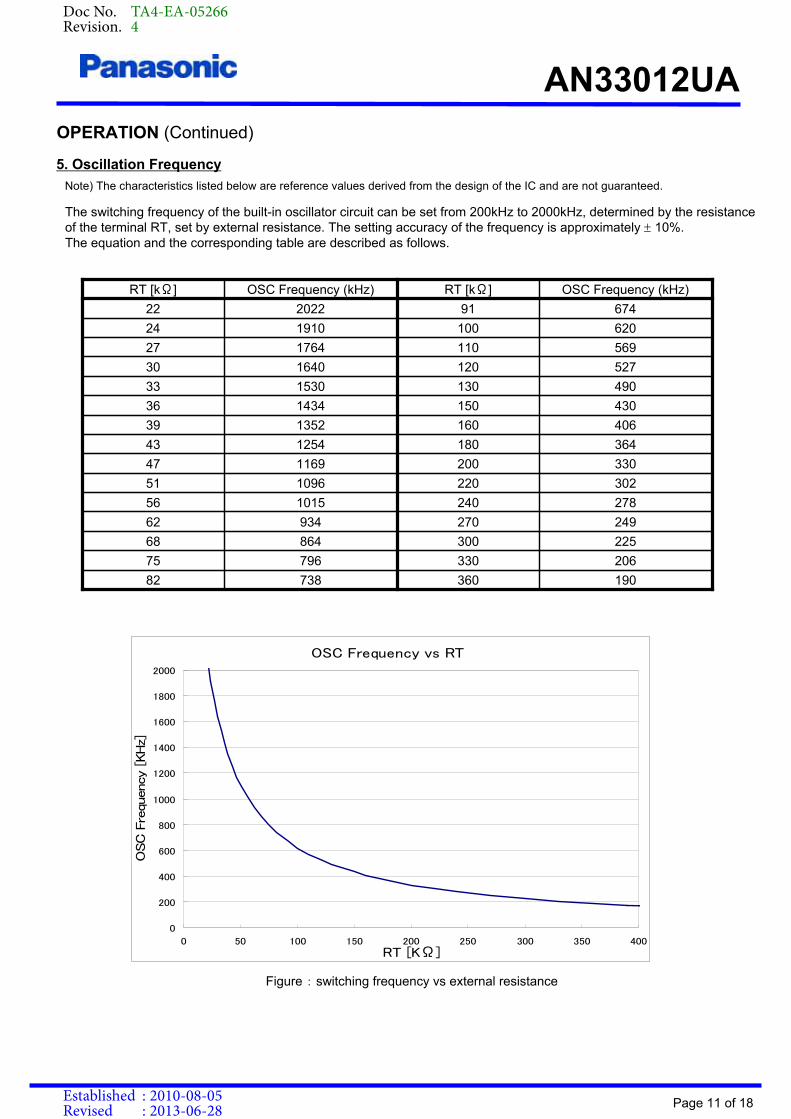
The switching frequency of the built-in oscillator circuit can be set from 200kHz to 2000kHz, determined by the resistanceof the terminal RT, set by external resistance. The setting accuracy of the frequency is approximately 10%. The equation and the corresponding table are described as follows.
OPERATION (Continued)
5. Oscillation Frequency
Note) The characteristics listed below are reference values derived from the design of the IC and are not guaranteed.
OSC Frequency vs RT
0
200
400
600
800
1000
1200
1400
1600
1800
2000
0 50 100 150 200 250 300 350 400
RT [KΩ]
OSC F
requency [KHz]
190 360738 82
206 330796 75
225 300864 68
249 270934 62
278 2401015 56
302 2201096 51
330 2001169 47
364 1801254 43
406 1601352 39
430 1501434 36
490 1301530 33
527 1201640 30
569 1101764 27
620 1001910 24
674 912022 22
OSC Frequency (kHz)RT [kΩ]OSC Frequency (kHz)RT [kΩ]
Figure : switching frequency vs external resistance
Doc No. TA4-EA-05266Revision. 4
Established : 2010-08-05Revised : 2013-06-28

AN33012UA
Page 12 of 18
Over-current protection function (OCP) turns off the Power MOS in IC when the voltage difference of the external resistance RSENSE exceeds 50mV(Typ.) to stop the supply of current from VCC to VOUT. Detection current ISENSE can be calculated as:
ISENSE = 50mV / RSENSE
The over-current protection function operates via pulse-by-pulse control, and Duty is limited during the over-currentprotection period. Moreover, because the over-current detects the peak current that flows through RSENSE, it isnecessary to convert it from desired output current IOUT value (Refer to Figure ). Equation is shown below.
OPERATION (Continued)
6. Over-Current Protection
Note) The characteristics listed below are reference values derived from the design of the IC and are not guaranteed.
Comp
VCC
LOGICVOUT
PowerMOS
IOUT
RLOAD
RSENSE
Figure : Over-Current Protection circuit block diagram
VCCLFVOUTVCCVOUT
IoutRsense
2)(
05.0
Inductor Current
IL
Average Current=IOUT
ISENSE
Iout
Detected current level (ISENSE)
IHigh
ILow
Figure : Method of detection of Over-Current Protection function
ISENSE
IL
Doc No. TA4-EA-05266Revision. 4
Established : 2010-08-05Revised : 2013-06-28

AN33012UA
Page 13 of 18
OPERATION (Continued)
When FB is equal or lower than 0.3 V, short current detection is triggered, FLAG pin will be pull to Low state. Theresponse timing is determined by TL pin capacitor value CTL (The response timing = CTL / 2A ×1.2V ).Note that the pull down current drivability of FLAG pin is 1.2 mA. Adjusting of FLAG response time in event of “over current” or “short current” condition is make possible by changing the capacitance of TL pin. In the event of over current detection, FLAG pin will be pull to Low state. Once FLAG is pull to Low state, it willremained at Low state until IC is reset through EN pin.
7. FLAG function after Over current / Short current detection
Note) The characteristics listed below are reference values derived from the design of the IC and are not guaranteed.
When the LSI internal temperature becomes more than about 165℃, TSD operates and DC-DC turns off.
9. Thermal Shut Down (TSD)
Note) The characteristics listed below are reference values derived from the design of the IC and are not guaranteed.
When FB is equal or higher than 1.22 V overvoltage detection is triggered, Power MOS will be off and LX will stop switching.
8. Over Voltage detection
Note) The characteristics listed below are reference values derived from the design of the IC and are not guaranteed.
10. Input Over Voltage protection
When VCC is equal or higher than 34V overvoltage detection is triggered, Power MOS will be off and LX will stopswitching.
Note) The characteristics listed below are reference values derived from the design of the IC and are not guaranteed.
Conclusion of protection functions
Stop ICwhen detected
Input Over Voltage
protection
Stop ICwhen detected
Stop switching CHthat abnormal is detected.
Output FLAG pinafter delay time
when detected in one side.(Reference below)
pulse-by-pulseis operated
independently
explanation
Thermal Shut DownOver Voltage detection
Over current / Short current detection
Over-Current Protection
Functionname
FLAG pin when over current / short current detection
pull-downabnormalabnormal
Hi-Znormalnormal
pull-downabnormalnormal
pull-downnormalabnormal
FLAGCH2CH1
Doc No. TA4-EA-05266Revision. 4
Established : 2010-08-05Revised : 2013-06-28

AN33012UA
Page 14 of 18
11. Channel- to-channel phase reversal
ERAMP
FB1 COMP1
PWM PRIDRV
CNT
ERAMP
FB2COMP2
PWM PRIDRV
LX1LX2 Phaseshift
0π VOUT1VOUT2
RAMP1RAMP2
ERA1ERA2
VINVIN
RAMP1
LX1
LX2
RAMP2
ERA2
ERA1
図 : Channel-to-channel phase reversal function Block diagram and timing chart
Note) The characteristics listed below are reference values derived from the design of the IC and are not guaranteed.
Sawtooth wave is superimposed to the reference input signal of each channel PWM, and it inverts timing ofswitching by to making phases sift 180 deg.
Doc No. TA4-EA-05266Revision. 4
Established : 2010-08-05Revised : 2013-06-28

AN33012UA
Page 15 of 18
This IC includes a soft start function whereby start-up time can be set to desired timing by adjusting the SS terminalcapacitor (Css). By adjusting the soft-start time, rush current from the Power supply terminal can be limited and the start-up timing of the output voltage can be changed. The timing chart and the method of selecting the external capacitor value is shown in below.
SSC
2.2μ
1.5(s) Time Start-Soft
EN
DC-DCoutput
SS
t
0.8V
Soft start time
2.3V
Figure : Soft start operation timing chart
Figure : Soft Start Time vs Css Value ( External Capacitor )
Equation to set soft start time by Css :
OPERATION (Continued)
12. Soft Start Timing and Setting
Note) The characteristics listed below are reference values derived from the design of the IC and are not guaranteed.
When this IC is used for power supply of communication with external equipment, the communication may notpossible during the soft-start period. Depending on the type of external equipment connected, in some cases, when the DC-DC is turned on, even though the soft start maybe halfway through, the voltage level is high enough to enablethe communication to start. In such cases, the micro-controller may not recognize the equipment normally and therefore it is required to set the micro-controller to access all possible equipment after the above soft-start setting time.
ソフトスタート時間 vs 外付けコンデンサ(Css)
0
0.020.04
0.06
0.08
0.10.12
0.14
0.16
0.18
0.2
0 20 40 60 80 100
ソフトスタート時間[ms]
Css
[uF]
Soft Start Time [ms]
Soft Start Time vs Css
Doc No. TA4-EA-05266Revision. 4
Established : 2010-08-05Revised : 2013-06-28
AN33012UA
Page 16 of 19
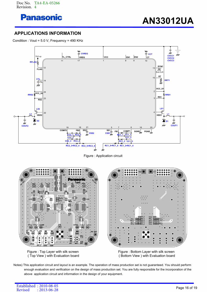
APPLICATIONS INFORMATION
Condition : Vout = 5.0 V, Frequency = 490 KHz
Figure : Application circuit
Figure : Top Layer with silk screen ( Top View ) with Evaluation board
Figure : Bottom Layer with silk screen ( Bottom View ) with Evaluation board
SS1FB1 COMP1 SGND PGND
HSD1
RS1
VCCVREG
17 1
SS2FB2COMP2
HSD2
RS2
VCC_S2
FLAG
Ext.CLK
SYNC
RT
13
15
2
3
4
2016675211819
22
23
24
12
10
14
CTEN1 EN2
8 9
TL
11
TL_CTRL
VCC_S1
Pull-up
RFLAG
RRT1
RRS1RRS2
L2 L1
LX1LX2
D1D2
COUT1COUT2
CVCC1CVCC2CVCC3
CCT
CTL
CVREG
CSS2 CSS1
RC2_3+RC2_4 RC2_5+RC2_6
RC2_2CC2_3
RC1_5+RC1_6 RC1_3+RC1_4
RC1_2 CC1_3
CC2_2 CC1_2RC2_1 RC1_1 CC1_1CC2_1
Notes) This application circuit and layout is an example. The operation of mass production set is not guaranteed. You should perform
enough evaluation and verification on the design of mass production set. You are fully responsible for the incorporation of the
above application circuit and information in the design of your equipment.
Doc No. TA4-EA-05266Revision. 4
Established : 2010-08-05Revised : 2013-06-28

AN33012UA
Page 17 of 19
APPLICATIONS INFORMATION ( Continued )
Figure : Recommended component
Compensation CapacitorMurata470pFGCM1882C1H471JA01JCC1_3,CC2_3
OCP Sense ResistorPanasonicR=11mERJ8BWFR011VRRS1,RRS2
OSC Setting ResistorPanasonicR=130kERA3AEB134VRRT1
PanasonicR=0ERJ3GEY0R00VRMOS1-2
Pull-up ResistorPanasonicR=200kERA3AEB204VRFLAG
Compensation & Feedback ResistorPanasonicR=1.5kERA3AEB152VRC1_2,RC2_2
Compensation & Feedback ResistorPanasonicR=0ERJ3GEY0R00VRC1_3,RC2_3,
RC1_6,RC2_6
Compensation & Feedback ResistorPanasonicR=7.5kERA3AEB752VRC1_1,RC2_1,
RC1_5,RC2_5
Schottky DiodePanasonic—DB24416D1,D2
2ch DC-DC ControllerPanasonic—AN33012UAIC1
InductorSUMIDA10µHCDRH8D43-100NCL1,L2
PMOSFETSANYO—ECH8305LX1,LX2
Output CapacitorTAIYO YUDEN22µFTMK325C7226MM-TCOUT1,COUT2
Input CapacitorTDK22µFCKG57NX7R1H226MTCVCC1,CVCC2,CVCC3
VREG CapacitorMurata1uFGCM188R71C105KA49JCVREG
Setting CapacitorMurata0.1uFGCM188R11C104KA01JCCT,CSS1,CSS2,CTL
Compensation CapacitorMurata27pFGCM1882C1H270JA01JCC1_2,CC2_2
Compensation CapacitorMurata2.2nFGCM1882C1H222JA01JCC1_1,CC2_1
DescriptionMakerValuePart NameReference
Doc No. TA4-EA-05266Revision. 4
Established : 2010-08-05Revised : 2013-06-28

AN33012UA
Page 18 of 19
PACKAGE INFORMATION ( Reference Data )
Outline Drawing
Unit : mm
Doc No. TA4-EA-05266Revision. 4
Established : 2010-08-05Revised : 2013-06-28

AN33012UA
Page 19 of 19
IMPORTANT NOTICE
1. When using the LSI for new models, verify the safety including the long-term reliability for each product.
2. When the application system is designed by using this LSI, please confirm the notes in this book. Please read the notes to descriptions and the usage notes in the book.
3. This LSI is intended to be used for general electronic equipment.Consult our sales staff in advance for information on the following applications: Special applications in which exceptional quality and reliability are required, or if the failure or malfunction of this LSI may directly jeopardize life or harm the human body.Any applications other than the standard applications intended.
(1) Space appliance (such as artificial satellite, and rocket)(2) Traffic control equipment (such as for airplane, train, and ship)(3) Medical equipment for life support(4) Submarine transponder(5) Control equipment for power plant(6) Disaster prevention and security device(7) Weapon(8) Others : Applications of which reliability equivalent to (1) to (7) is required
Our company shall not be held responsible for any damage incurred as a result of or in connection with the LSI being used for any special application, unless our company agrees to the use of such special application.
4. Please use this product in compliance with all applicable laws and regulations that regulate the inclusion or use of controlled substances, including without limitation, the EU RoHS Directive. Our company shall not be held responsible for any damage incurred as a result of our LSI being used by our customers, not complying with the applicable laws and regulations.
5. Pay attention to the direction of LSI. When mounting it in the wrong direction onto the PCB (printed-circuit-board), it might emit smoke or ignite.
6. Pay attention in the PCB (printed-circuit-board) pattern layout in order to prevent damage due to short circuit between pins. In addition, refer to the Pin Description for the pin configuration.
7. Perform a visual inspection on the PCB before applying power, otherwise damage might happen due to problems such as a solder-bridge between the pins of the semiconductor device. Also, perform a full technical verification on the assembly quality, because the same damage possibly can happen due to conductive substances, such as solder ball, that adhere to the LSI during transportation.
8. Take notice in the use of this product that it might be damaged or occasionally emit smoke when an abnormal state occurs such as output pin-VCC short (Power supply fault), output pin-GND short (Ground fault), or output-to-output-pin short (load short). Safety measures such as an installation of fuses are recommended because the extent of the above-mentioned damage and smoke emission will depend on the current capability of the power supply..
9. The protection circuit is for maintaining safety against abnormal operation. Therefore, the protection circuit should not work during normal operation.Especially for the thermal protection circuit, if the area of safe operation or the absolute maximum rating is momentarily exceeded due to output pin to VCC short (Power supply fault), or output pin to GND short (Ground fault), the LSI might be damaged before the thermal protection circuit could operate.
10. Unless specified in the product specifications, make sure that negative voltage or excessive voltage are not applied to thepins because the device might be damaged, which could happen due to negative voltage or excessive voltage generated during the ON and OFF timing when the inductive load of a motor coil or actuator coils of optical pick-up is being driven.
11. Product which has specified ASO (Area of Safe Operation) should be operated in ASO
12. Verify the risks which might be caused by the malfunctions of external components.
Doc No. TA4-EA-05266Revision. 4
Established : 2010-08-05Revised : 2013-06-28

Request for your special attention and precautions in using the technical information and semiconductors described in this book
(1) If any of the products or technical information described in this book is to be exported or provided to non-residents, the
laws and regulations of the exporting country, especially, those with regard to security export control, must be observed. (2) The technical information described in this book is intended only to show the main characteristics and application circuit
examples of the products. No license is granted in and to any intellectual property right or other right owned by Panasonic Corporation or any other company. Therefore, no responsibility is assumed by our company as to the infringement upon any such right owned by any other company which may arise as a result of the use of technical information de-scribed in this book.
(3) The products described in this book are intended to be used for general applications (such as office equipment,
communications equipment, measuring instruments and household appliances), or for specific applications as expressly stated in this book.
Please consult with our sales staff in advance for information on the following applications, moreover please exchange documents separately on terms of use etc.: Special applications (such as for in-vehicle equipment, airplanes, aerospace, automotive equipment, traffic signaling equipment, combustion equipment, medical equipment and safety devices) in which exceptional quality and reliability are required, or if the failure or malfunction of the products may directly jeopardize life or harm the human body.
Unless exchanging documents on terms of use etc. in advance, it is to be understood that our company shall not be held responsible for any damage incurred as a result of or in connection with your using the products described in this book for any special application.
(4) The products and product specifications described in this book are subject to change without notice for modification and/or
improvement. At the final stage of your design, purchasing, or use of the products, therefore, ask for the most up-to-date Product Standards in advance to make sure that the latest specifications satisfy your requirements.
(5) When designing your equipment, comply with the range of absolute maximum rating and the guaranteed operating
conditions (operating power supply voltage and operating environment etc.). Especially, please be careful not to exceed the range of absolute maximum rating on the transient state, such as power-on, power-off and mode-switching. Other-wise, we will not be liable for any defect which may arise later in your equipment.
Even when the products are used within the guaranteed values, take into the consideration of incidence of break down and failure mode, possible to occur to semiconductor products. Measures on the systems such as redundant design, arresting the spread of fire or preventing glitch are recommended in order to prevent physical injury, fire, social damages, for example, by using the products.
(6) Comply with the instructions for use in order to prevent breakdown and characteristics change due to external factors (ESD,
EOS, thermal stress and mechanical stress) at the time of handling, mounting or at customer's process. We do not guarantee quality for disassembled products or the product re-mounted after removing from the mounting board.
When using products for which damp-proof packing is required, satisfy the conditions, such as shelf life and the elapsed time since first opening the packages.
(7) When reselling products described in this book to other companies without our permission and receiving any claim of
request from the resale destination, please understand that customers will bear the burden. (8) This book may be not reprinted or reproduced whether wholly or partially, without the prior written permission of our
company.
No.010618