Embed Size (px)
Citation preview
IEEE JOURNAL OF SOLID-STATE CIRCUITS, VOL. 38, NO. 7, JULY 2003 1123
An Ultralow-Energy ADC for Smart DustMichael D. Scott, Student Member, IEEE, Bernhard E. Boser, Fellow, IEEE, and Kristofer S. J. Pister, Member, IEEE
Abstract—A low-energy successive approximation analog-to-digital converter (ADC) targeted for use in distributed sensornetworks is presented. The individual nodes combine sensing,computation, communications, and power into a tiny volume.Energy is extremely limited, forcing the nodes to operate withvery low duty cycles. This paper describes the design and imple-mentation of an ADC to meet the unique requirements of sensornetworks. The ADC reported here consumes 31 pJ/8-bit sample at1-V supply and 100 kS/s, with a standby power consumption of 70pW. This energy consumption is one of the lowest ever reported.
Index Terms—Analog-to-digital converter (ADC), charge redis-tribution, CMOS, energy, low power, sensor networks, Smart Dust,successive approximation.
I. INTRODUCTION
I N THE PAST decade, much of the research on analog-to-digital converters (ADCs) has focused on increasing sam-
pling rate and resolution. While there are many applications thatdemand such advances, other emerging applications do not re-quire high performance but do place very stringent requirementson energy consumption. This paper focuses on a portion of theADC design space that has received comparatively little atten-tion—moderate resolution and speed, but ultralow power.
Such ADCs are critical components in large-scale wirelesssensor networks. The vanishing size and cost of the individualnodes in these sensor networks will allow them to interactwith the environment in far less intrusive ways than previousnetworked sensor systems. Potential applications range fromsmart building environments, tracking wildlife populations,monitoring crops and livestock, and measuring and predictingweather patterns. The energy consumption of the nodes willdetermine both the lifetime of the individual nodes and thescope of possible applications.
The ADC is the interface between the sensed environmentand the sensor network as a whole, so its performance and flex-ibility are critical. Low active and standby power is paramount,but there are other considerations as well. The remainder of thispaper describes the design and implementation of an ADC tomeet the unique requirements of distributed sensor networks.While targeted for sensor networks, the ADC presented here isalso well suited for other energy-constrained systems, such aslow-resolution CMOS imaging systems [1] or microrobotic sys-tems [2].
The organization of this paper is as follows. Section II in-troduces the target application for the ADC and details the de-
Manuscript received November 27, 2002; revised February 24, 2003.The authors are with the Berkeley Sensor and Actuator Center, Department
of Electrical Engineering and Computer Science, University of California,Berkeley, CA 94720-1770 USA (e-mail: [email protected];[email protected]; [email protected]).
Digital Object Identifier 10.1109/JSSC.2003.813296
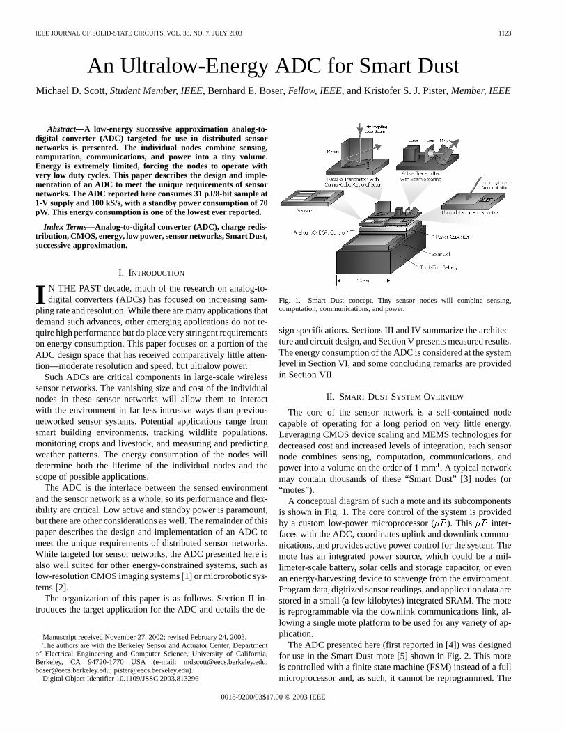
Fig. 1. Smart Dust concept. Tiny sensor nodes will combine sensing,computation, communications, and power.
sign specifications. Sections III and IV summarize the architec-ture and circuit design, and Section V presents measured results.The energy consumption of the ADC is considered at the systemlevel in Section VI, and some concluding remarks are providedin Section VII.
II. SMART DUST SYSTEM OVERVIEW
The core of the sensor network is a self-contained nodecapable of operating for a long period on very little energy.Leveraging CMOS device scaling and MEMS technologies fordecreased cost and increased levels of integration, each sensornode combines sensing, computation, communications, andpower into a volume on the order of 1 mm. A typical networkmay contain thousands of these “Smart Dust” [3] nodes (or“motes”).
A conceptual diagram of such a mote and its subcomponentsis shown in Fig. 1. The core control of the system is providedby a custom low-power microprocessor (). This inter-faces with the ADC, coordinates uplink and downlink commu-nications, and provides active power control for the system. Themote has an integrated power source, which could be a mil-limeter-scale battery, solar cells and storage capacitor, or evenan energy-harvesting device to scavenge from the environment.Program data, digitized sensor readings, and application data arestored in a small (a few kilobytes) integrated SRAM. The moteis reprogrammable via the downlink communications link, al-lowing a single mote platform to be used for any variety of ap-plication.
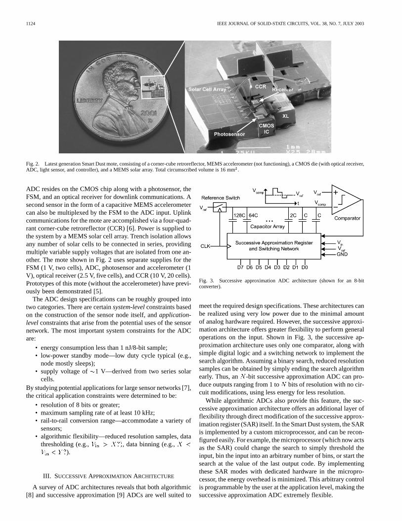
The ADC presented here (first reported in [4]) was designedfor use in the Smart Dust mote [5] shown in Fig. 2. This moteis controlled with a finite state machine (FSM) instead of a fullmicroprocessor and, as such, it cannot be reprogrammed. The
0018-9200/03$17.00 © 2003 IEEE
1124 IEEE JOURNAL OF SOLID-STATE CIRCUITS, VOL. 38, NO. 7, JULY 2003
Fig. 2. Latest generation Smart Dust mote, consisting of a corner-cube retroreflector, MEMS accelerometer (not functioning), a CMOS die (with optical receiver,ADC, light sensor, and controller), and a MEMS solar array. Total circumscribed volume is 16 mm.
ADC resides on the CMOS chip along with a photosensor, theFSM, and an optical receiver for downlink communications. Asecond sensor in the form of a capacitive MEMS accelerometercan also be multiplexed by the FSM to the ADC input. Uplinkcommunications for the mote are accomplished via a four-quad-rant corner-cube retroreflector (CCR) [6]. Power is supplied tothe system by a MEMS solar cell array. Trench isolation allowsany number of solar cells to be connected in series, providingmultiple variable supply voltages that are isolated from one an-other. The mote shown in Fig. 2 uses separate supplies for theFSM (1 V, two cells), ADC, photosensor and accelerometer (1V), optical receiver (2.5 V, five cells), and CCR (10 V, 20 cells).Prototypes of this mote (without the accelerometer) have previ-ously been demonstrated [5].
The ADC design specifications can be roughly grouped intotwo categories. There are certainsystem-levelconstraints basedon the construction of the sensor node itself, andapplication-levelconstraints that arise from the potential uses of the sensornetwork. The most important system constraints for the ADCare:
• energy consumption less than 1 nJ/8-bit sample;• low-power standby mode—low duty cycle typical (e.g.,
node mostly sleeps);• supply voltage of 1 V—derived from two series solar
cells.By studying potential applications for large sensor networks [7],the critical application constraints were determined to be:
• resolution of 8 bits or greater;• maximum sampling rate of at least 10 kHz;• rail-to-rail conversion range—accommodate a variety of
sensors;• algorithmic flexibility—reduced resolution samples, data
thresholding (e.g., , data binning (e.g.,).
III. SUCCESSIVEAPPROXIMATION ARCHITECTURE
A survey of ADC architectures reveals that both algorithmic[8] and successive approximation [9] ADCs are well suited to
Fig. 3. Successive approximation ADC architecture (shown for an 8-bitconverter).
meet the required design specifications. These architectures canbe realized using very low power due to the minimal amountof analog hardware required. However, the successive approxi-mation architecture offers greater flexibility to perform generaloperations on the input. Shown in Fig. 3, the successive ap-proximation architecture uses only one comparator, along withsimple digital logic and a switching network to implement thesearch algorithm. Assuming a binary search, reduced resolutionsamples can be obtained by simply ending the search algorithmearly. Thus, an -bit successive approximation ADC can pro-duce outputs ranging from 1 to bits of resolution with no cir-cuit modifications, using less energy for less resolution.
While algorithmic ADCs also provide this feature, the suc-cessive approximation architecture offers an additional layer offlexibility through direct modification of the successive approx-imation register (SAR) itself. In the Smart Dust system, the SARis implemented by a custom microprocessor, and can be recon-figured easily. For example, the microprocessor (which now actsas the SAR) could change the search to simply threshold theinput, bin the input into an arbitrary number of bins, or start thesearch at the value of the last output code. By implementingthese SAR modes with dedicated hardware in the micropro-cessor, the energy overhead is minimized. This arbitrary controlis programmable by the user at the application level, making thesuccessive approximation ADC extremely flexible.
SCOTTet al.: ULTRALOW-ENERGY ADC FOR SMART DUST 1125
The operation of the ADC is as follows. First, the inputvoltage is sampled onto the capacitor array. Next, the SARgenerates an approximation, which is converted to a voltageat by the capacitor array and compared to by thecomparator. The SAR uses the comparator result to computeits next approximation for the digital code. A standard binarysearch algorithm leads to an-bit output available after the
th comparison.
IV. ADC CIRCUIT DESIGN
As seen in Fig. 3, the successive approximation architecturerequires a reference voltage to charge the capacitors during theconversion cycle. Often this reference voltage is derived from abandgap circuit, and therefore requires power. To avoid on-chipreference generation, the reference voltage was chosen to be thesupply voltage, which is already present on-chip. In addition tosaving power, this choice has a number of additional benefits.First, it allows the use of simple pMOS devices for switching thereference onto the capacitors. Second, the comparator now op-erates with a threshold voltage equal to the supply voltage
. This allows the comparator to be realized with a conven-tional nMOS differential pair input, despite the relatively low1-V supply. Finally, this sets the input conversion range of theconverter to be rail-to-rail.
One potential difficulty with choosing is thepower-supply rejection (PSR) of the converter. As (and,hence, ) varies, the output codes adjust accordingly. Theproblem is aggravated because the supply voltage is derivedfrom solar cells that vary substantially with the ambient light.Fortunately, many sensors (e.g., bridge sensors) are ratiometricwith , which means that the overall sensor-ADC subsystemmaintains reasonable PSR despite large absolute variations insupply. For nonratiometric sensors, however, poor supply rejec-tion is inherent and must be tolerated at the application level.
A. Capacitor Array
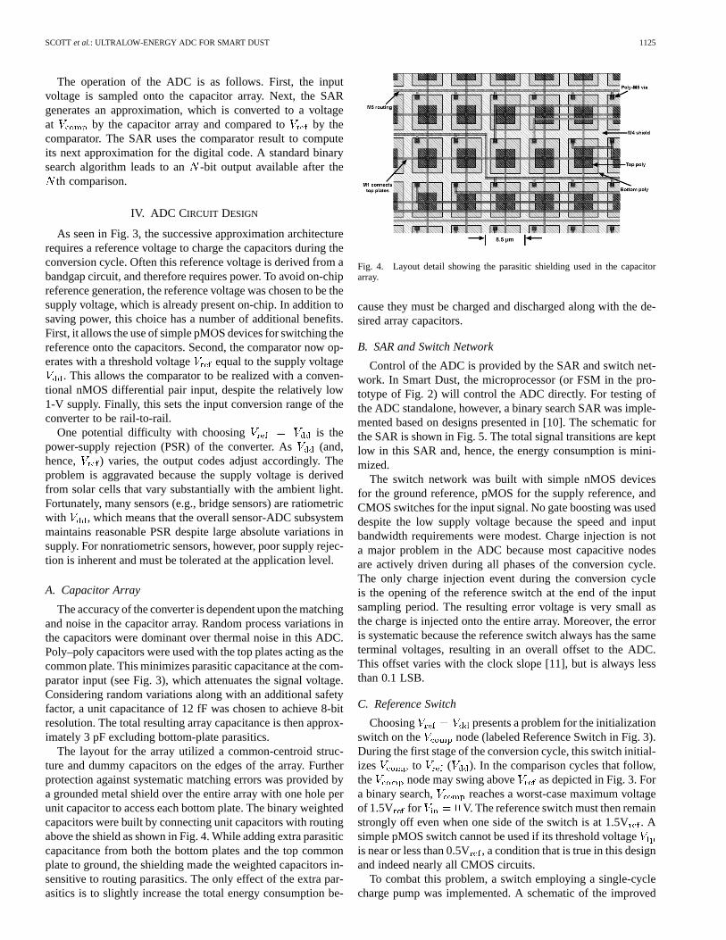
The accuracy of the converter is dependent upon the matchingand noise in the capacitor array. Random process variations inthe capacitors were dominant over thermal noise in this ADC.Poly–poly capacitors were used with the top plates acting as thecommon plate. This minimizes parasitic capacitance at the com-parator input (see Fig. 3), which attenuates the signal voltage.Considering random variations along with an additional safetyfactor, a unit capacitance of 12 fF was chosen to achieve 8-bitresolution. The total resulting array capacitance is then approx-imately 3 pF excluding bottom-plate parasitics.
The layout for the array utilized a common-centroid struc-ture and dummy capacitors on the edges of the array. Furtherprotection against systematic matching errors was provided bya grounded metal shield over the entire array with one hole perunit capacitor to access each bottom plate. The binary weightedcapacitors were built by connecting unit capacitors with routingabove the shield as shown in Fig. 4. While adding extra parasiticcapacitance from both the bottom plates and the top commonplate to ground, the shielding made the weighted capacitors in-sensitive to routing parasitics. The only effect of the extra par-asitics is to slightly increase the total energy consumption be-
Fig. 4. Layout detail showing the parasitic shielding used in the capacitorarray.
cause they must be charged and discharged along with the de-sired array capacitors.
B. SAR and Switch Network
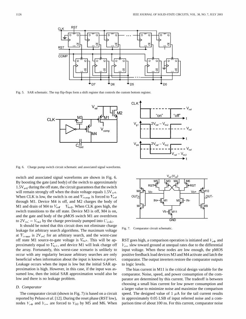
Control of the ADC is provided by the SAR and switch net-work. In Smart Dust, the microprocessor (or FSM in the pro-totype of Fig. 2) will control the ADC directly. For testing ofthe ADC standalone, however, a binary search SAR was imple-mented based on designs presented in [10]. The schematic forthe SAR is shown in Fig. 5. The total signal transitions are keptlow in this SAR and, hence, the energy consumption is mini-mized.
The switch network was built with simple nMOS devicesfor the ground reference, pMOS for the supply reference, andCMOS switches for the input signal. No gate boosting was useddespite the low supply voltage because the speed and inputbandwidth requirements were modest. Charge injection is nota major problem in the ADC because most capacitive nodesare actively driven during all phases of the conversion cycle.The only charge injection event during the conversion cycleis the opening of the reference switch at the end of the inputsampling period. The resulting error voltage is very small asthe charge is injected onto the entire array. Moreover, the erroris systematic because the reference switch always has the sameterminal voltages, resulting in an overall offset to the ADC.This offset varies with the clock slope [11], but is always lessthan 0.1 LSB.
C. Reference Switch
Choosing presents a problem for the initializationswitch on the node (labeled Reference Switch in Fig. 3).During the first stage of the conversion cycle, this switch initial-izes to ( ). In the comparison cycles that follow,the node may swing above as depicted in Fig. 3. Fora binary search, reaches a worst-case maximum voltageof 1.5V for V. The reference switch must then remainstrongly off even when one side of the switch is at 1.5V. Asimple pMOS switch cannot be used if its threshold voltageis near or less than 0.5V, a condition that is true in this designand indeed nearly all CMOS circuits.
To combat this problem, a switch employing a single-cyclecharge pump was implemented. A schematic of the improved
1126 IEEE JOURNAL OF SOLID-STATE CIRCUITS, VOL. 38, NO. 7, JULY 2003
Fig. 5. SAR schematic. The top flip-flops form a shift register that controls the custom bottom register.
Fig. 6. Charge pump switch circuit schematic and associated signal waveforms.
switch and associated signal waveforms are shown in Fig. 6.By boosting the gate (and body) of the switch to approximately1.5V during the off state, the circuit guarantees that the switchwill remain strongly off when the drain voltage equals 1.5V.When CLK is low, the switch is on and is forced tothrough M1. Device M4 is off, and M2 charges the body ofM1 and drain of M4 to . When CLK goes high, theswitch transitions to the off state. Device M3 is off, M4 is on,and the gate and body of the pMOS switch M1 are overdrivento 2V by the charge previously pumped into .
It should be noted that this circuit does not eliminate chargeleakage for arbitrary search algorithms. The maximum voltageat is 2V for an arbitrary search, and the worst-caseoff state M1 source-to-gate voltage is . This will be ap-proximately equal to , and device M1 will leak charge offthe array. Fortunately, this worst-case scenario is unlikely tooccur with any regularity because arbitrary searches are onlybeneficial when information about the input is knowna priori.Leakage occurs when the input is low but the initial SAR ap-proximation is high. However, in this case, if the input was as-sumed low, then the initial SAR approximation would also below and there is no leakage problem.
D. Comparator
The comparator circuit (shown in Fig. 7) is based on a circuitreported by Pelusoet al.[12]. During the reset phase (RST low),nodes and are forced to by M5 and M6. When
Fig. 7. Comparator circuit schematic.
RST goes high, a comparison operation is initiated andandslew toward ground at unequal rates due to the differential
input voltage. When these nodes are low enough, the pMOSpositive feedback load devices M3 and M4 activate and latch thecomparator. The output inverters restore the comparator outputsto logic levels.
The bias current in M11 is the critical design variable for thecomparator. Noise, speed, and power consumption of the com-parator are determined by this current. The tradeoff is betweenchoosing a small bias current for low power consumption anda larger value to minimize noise and maximize the comparisonspeed. The designed value of 1A for the tail current resultsin approximately 0.05 LSB of input referred noise and a com-parison time of about 100 ns. For this current, comparator noise
SCOTTet al.: ULTRALOW-ENERGY ADC FOR SMART DUST 1127
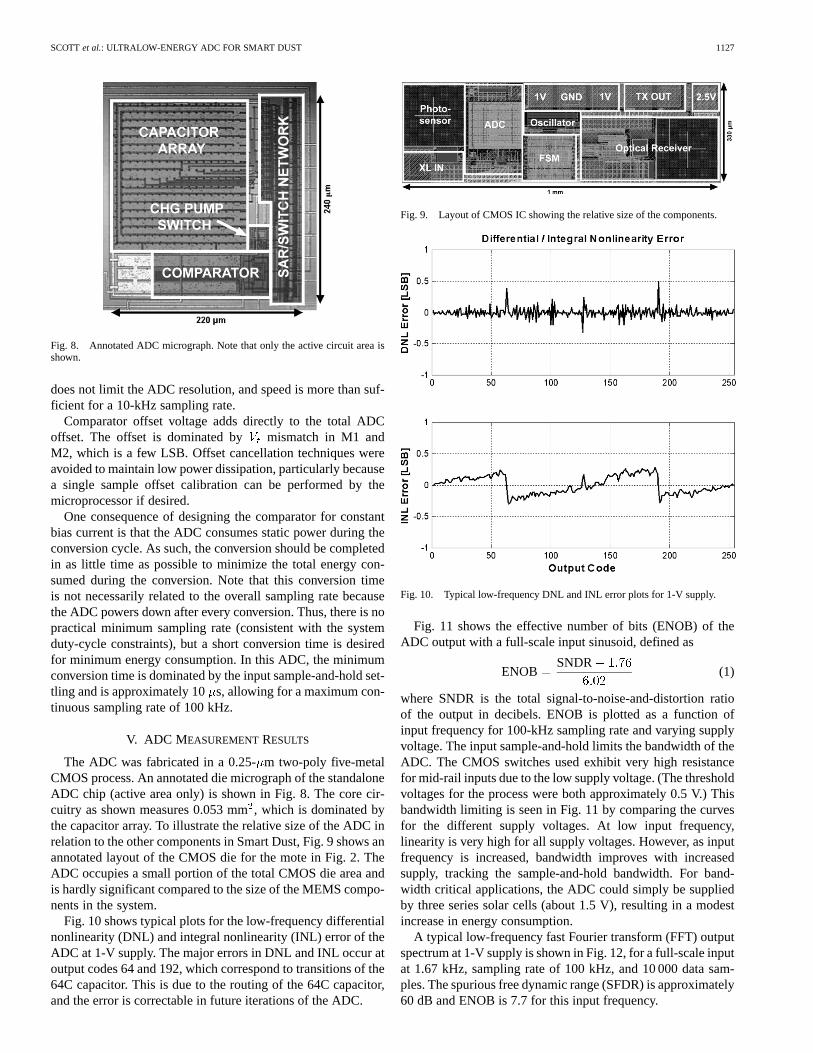
Fig. 8. Annotated ADC micrograph. Note that only the active circuit area isshown.
does not limit the ADC resolution, and speed is more than suf-ficient for a 10-kHz sampling rate.
Comparator offset voltage adds directly to the total ADCoffset. The offset is dominated by mismatch in M1 andM2, which is a few LSB. Offset cancellation techniques wereavoided to maintain low power dissipation, particularly becausea single sample offset calibration can be performed by themicroprocessor if desired.
One consequence of designing the comparator for constantbias current is that the ADC consumes static power during theconversion cycle. As such, the conversion should be completedin as little time as possible to minimize the total energy con-sumed during the conversion. Note that this conversion timeis not necessarily related to the overall sampling rate becausethe ADC powers down after every conversion. Thus, there is nopractical minimum sampling rate (consistent with the systemduty-cycle constraints), but a short conversion time is desiredfor minimum energy consumption. In this ADC, the minimumconversion time is dominated by the input sample-and-hold set-tling and is approximately 10s, allowing for a maximum con-tinuous sampling rate of 100 kHz.
V. ADC MEASUREMENTRESULTS
The ADC was fabricated in a 0.25-m two-poly five-metalCMOS process. An annotated die micrograph of the standaloneADC chip (active area only) is shown in Fig. 8. The core cir-cuitry as shown measures 0.053 mm, which is dominated bythe capacitor array. To illustrate the relative size of the ADC inrelation to the other components in Smart Dust, Fig. 9 shows anannotated layout of the CMOS die for the mote in Fig. 2. TheADC occupies a small portion of the total CMOS die area andis hardly significant compared to the size of the MEMS compo-nents in the system.
Fig. 10 shows typical plots for the low-frequency differentialnonlinearity (DNL) and integral nonlinearity (INL) error of theADC at 1-V supply. The major errors in DNL and INL occur atoutput codes 64 and 192, which correspond to transitions of the64C capacitor. This is due to the routing of the 64C capacitor,and the error is correctable in future iterations of the ADC.
Fig. 9. Layout of CMOS IC showing the relative size of the components.
Fig. 10. Typical low-frequency DNL and INL error plots for 1-V supply.
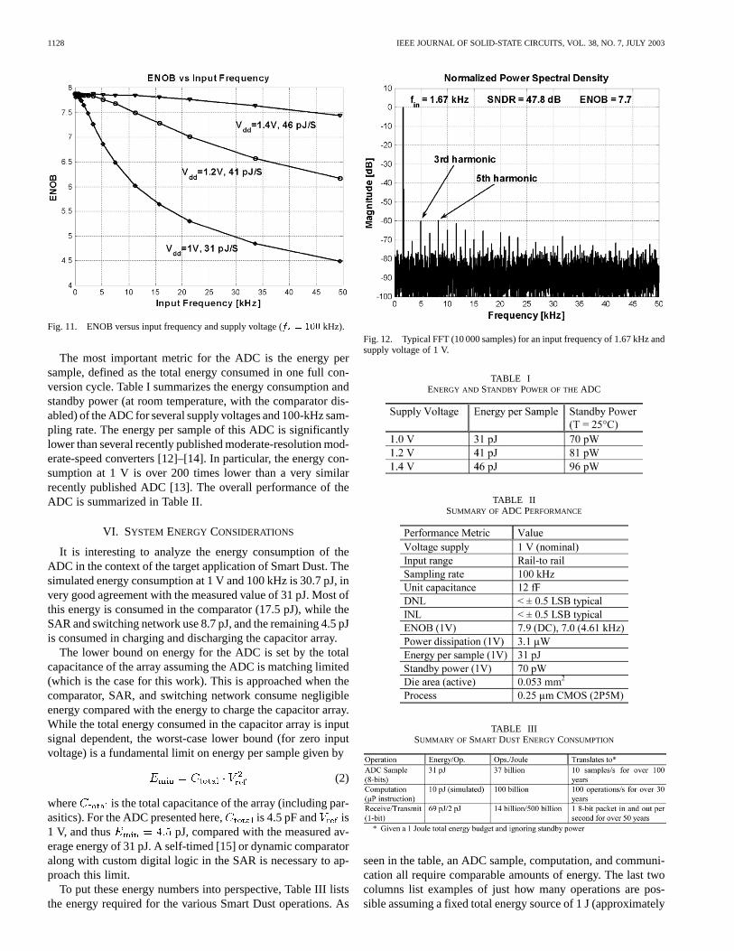
Fig. 11 shows the effective number of bits (ENOB) of theADC output with a full-scale input sinusoid, defined as
ENOBSNDR
(1)
where SNDR is the total signal-to-noise-and-distortion ratioof the output in decibels. ENOB is plotted as a function ofinput frequency for 100-kHz sampling rate and varying supplyvoltage. The input sample-and-hold limits the bandwidth of theADC. The CMOS switches used exhibit very high resistancefor mid-rail inputs due to the low supply voltage. (The thresholdvoltages for the process were both approximately 0.5 V.) Thisbandwidth limiting is seen in Fig. 11 by comparing the curvesfor the different supply voltages. At low input frequency,linearity is very high for all supply voltages. However, as inputfrequency is increased, bandwidth improves with increasedsupply, tracking the sample-and-hold bandwidth. For band-width critical applications, the ADC could simply be suppliedby three series solar cells (about 1.5 V), resulting in a modestincrease in energy consumption.
A typical low-frequency fast Fourier transform (FFT) outputspectrum at 1-V supply is shown in Fig. 12, for a full-scale inputat 1.67 kHz, sampling rate of 100 kHz, and 10 000 data sam-ples. The spurious free dynamic range (SFDR) is approximately60 dB and ENOB is 7.7 for this input frequency.
1128 IEEE JOURNAL OF SOLID-STATE CIRCUITS, VOL. 38, NO. 7, JULY 2003
Fig. 11. ENOB versus input frequency and supply voltage (f = 100 kHz).
The most important metric for the ADC is the energy persample, defined as the total energy consumed in one full con-version cycle. Table I summarizes the energy consumption andstandby power (at room temperature, with the comparator dis-abled) of the ADC for several supply voltages and 100-kHz sam-pling rate. The energy per sample of this ADC is significantlylower than several recently published moderate-resolution mod-erate-speed converters [12]–[14]. In particular, the energy con-sumption at 1 V is over 200 times lower than a very similarrecently published ADC [13]. The overall performance of theADC is summarized in Table II.
VI. SYSTEM ENERGY CONSIDERATIONS
It is interesting to analyze the energy consumption of theADC in the context of the target application of Smart Dust. Thesimulated energy consumption at 1 V and 100 kHz is 30.7 pJ, invery good agreement with the measured value of 31 pJ. Most ofthis energy is consumed in the comparator (17.5 pJ), while theSAR and switching network use 8.7 pJ, and the remaining 4.5 pJis consumed in charging and discharging the capacitor array.
The lower bound on energy for the ADC is set by the totalcapacitance of the array assuming the ADC is matching limited(which is the case for this work). This is approached when thecomparator, SAR, and switching network consume negligibleenergy compared with the energy to charge the capacitor array.While the total energy consumed in the capacitor array is inputsignal dependent, the worst-case lower bound (for zero inputvoltage) is a fundamental limit on energy per sample given by
(2)
where is the total capacitance of the array (including par-asitics). For the ADC presented here, is 4.5 pF and is1 V, and thus pJ, compared with the measured av-erage energy of 31 pJ. A self-timed [15] or dynamic comparatoralong with custom digital logic in the SAR is necessary to ap-proach this limit.
To put these energy numbers into perspective, Table III liststhe energy required for the various Smart Dust operations. As
Fig. 12. Typical FFT (10 000 samples) for an input frequency of 1.67 kHz andsupply voltage of 1 V.
TABLE IENERGY AND STANDBY POWER OF THEADC
TABLE IISUMMARY OF ADC PERFORMANCE
TABLE IIISUMMARY OF SMART DUST ENERGY CONSUMPTION
seen in the table, an ADC sample, computation, and communi-cation all require comparable amounts of energy. The last twocolumns list examples of just how many operations are pos-sible assuming a fixed total energy source of 1 J (approximately

SCOTTet al.: ULTRALOW-ENERGY ADC FOR SMART DUST 1129
10 000 times less energy than an alkaline AA battery) and ne-glecting standby power. Including the standby power, this ADCcould take ten samples per second for over 40 years from a 1-Jenergy budget (down from 100 years when neglecting leakage).
VII. CONCLUSION
An 8-bit 100-kS/s 1-V ADC was presented for use in sensornetwork applications. After introducing the target applicationand resulting design constraints, the actual ADC design was de-tailed. An energy consumption of 31 pJ per sample was achievedusing a charge redistribution successive approximation architec-ture. Analysis of the full sensor node energy constraints showedthat this ADC sample energy was comparable to the energy costof the other relevant system operations. Example scenarios illus-trated the extraordinary number of operations possible for theseenergy efficient sensor nodes even with very little total energyavailable over the node lifetime.
ACKNOWLEDGMENT
The authors would like to thank the rest of the SmartDust research team at the University of California, Berkeley:B. Warneke, B. Leibowitz, C. Bellew, and L. Zhou. B. Lei-bowitz in particular provided valuable discussion throughoutthe ADC design process. R. Lu assisted in the layout of aprototype ADC. The ADC and other CMOS componentsfor Smart Dust were fabricated in a National Semiconductor0.25- m CMOS process.
REFERENCES
[1] Z. Zhou, B. Pain, and E. R. Fossum, “CMOS active pixel sensor withon-chip successive approximation analog-to-digital converter,”IEEETrans. Electron Devices, vol. 44, pp. 1759–1763, Oct. 1997.
[2] R. Yeh and K. S. J. Pister, “Design of low-power articulated micro-robots,” in Proc. Int. Conf. Robotics and Automation, Workshop onMobil Micro-Robots, San Francisco, CA, Apr. 2000, pp. 21–28.
[3] B. Warneke, B. Atwood, and K. S. J. Pister, “Smart Dust mote forerun-ners,” inProc. 14th Annu. Int. Conf. Microelectromechanical Systems(MEMS 2001), Interlaken, Switzerland, Jan. 2001, pp. 357–360.
[4] M. D. Scott, B. E. Boser, and K. S. J. Pister, “An ultra-low power ADCfor distributed sensor networks,” inProc. 28th Eur. Solid-State CircuitsConf., Florence, Italy, Sept. 2002, pp. 255–258.
[5] B. A. Warnekeet al., “An autonomous 16 mmsolar-powered node fordistributed wireless sensor networks,” inProc. IEEE Sensors 2002, Or-lando, FL, June 2002, pp. 1510–1515.
[6] L. Zhou, K. S. J. Pister, and J. M. Kahn, “Assembled corner-cube retrore-flector quadruplet,” inProc. 15th Annu. Int. Conf. Microelectromechan-ical Systems (MEMS 2002), Las Vegas, NV, Jan. 2002, pp. 556–559.
[7] L. Doherty, B. A. Warneke, B. E. Boser, and K. S. J. Pister, “Energyand performance considerations for Smart Dust,”Int. J. Parallel Distrib.Syst. Networks, vol. 4, no. 3, pp. 121–133, 2001.
[8] A. M. Mallinson and P. Spitalny, “A 17b algorithmic ADC,” inIEEEInt. Solid-State Circuits Conf. Dig. Tech. Papers, San Francisco, CA,Feb. 1992, pp. 40–41.
[9] D. A. Johns and K. Martin,Analog Integrated Circuit Design. NewYork: Wiley, 1997.
[10] T. O. Anderson, “Optimum control logic for successive approximationA–D converters,”Comput. Design, vol. 11, no. 7, pp. 81–86, July 1972.
[11] G. Wegmann, E. A. Vittoz, and F. Rahali, “Charge injection inanalog MOS switches,”IEEE J. Solid-State Circuits, vol. SC-22, pp.1091–1097, Dec. 1987.
[12] V. Peluso, P. Vancorenland, A. M. Marques, M. S. J. Steyaert, and W.Sansen, “A 900-mV low-power�� A/D converter with 77-dB dynamicrange,”IEEE J. Solid-State Circuits, vol. 33, pp. 1887–1897, Dec. 1998.
[13] S. Mortezapour and E. K. F. Lee, “A 1-V 8-bit successive approximationADC in standard CMOS process,”IEEE J. Solid-State Circuits, vol. 35,pp. 642–646, Apr. 2000.
[14] D.-Y. Chang and S.-H. Lee, “Design techniques for a low-powerlow-cost CMOS A/D converter,”IEEE J. Solid-State Circuits, vol. 33,pp. 1244–1248, Aug. 1998.
[15] G. Promitzeir, “12 bit low power fully differential switched capacitornoncalibrating successive approximation ADC with 1 MS/s,” inProc.26th Eur. Solid-State Circuits Conf., Stockholm, Sweden, Sept. 2000,pp. 368–371.
Michael D. Scott (S’00) received the B.S. degree inelectrical and computer engineering from CarnegieMellon University, Pittsburgh, PA, in 1999, and theM.S. degree in electrical engineering from the Uni-versity of California, Berkeley, in 2002. He is cur-rently working toward the Ph.D. degree in electricalengineering with a focus on low-power analog cir-cuits at the University of California, Berkeley.
He has held internships at Orbital Sciences Corpo-ration (formerly CTA Space Systems), Bose Corpo-ration, and National Instruments Corporation, where
he worked on satellite ground station equipment, radio frequency immunity testsystems, and data acquisition hardware design, respectively. He spent most of2000 at MIT Lincoln Laboratories, where his work focused on RF hardware forman-portable EHF communications terminals.
Bernhard E. Boser (S’79–M’83–F’03) received theDiploma in electrical engineering from the SwissFederal Institute of Technology, Zurich, in 1984and the M.S. and Ph.D. from Stanford University,Stanford, CA, in 1985 and 1988, respectively.
From 1988 to 1992, he was a Member of Tech-nical Staff in the Adaptive Systems Department,AT&T Bell Laboratories. In 1992, he joined thefaculty of the Department of Electrical Engineeringand Computer Science, University of California,Berkeley, where he also serves as a Director of the
Berkeley Sensor and Actuator Center. His research is in the area of analog andmixed-signal circuits, with special emphasis on micromechanical sensors andactuators.
Dr. Boser has served on the program committees of the IEEE InternationalSolid-State Circuits Conference, the Transducers Conference, and the VLSISymposium. He is currently the Editor-in-Chief of the IEEE JOURNAL OFSOLID-STATE CIRCUITS.
Kristofer S. J. Pister (M’02) received the B.A. de-gree in applied physics from the University of Cali-fornia, San Diego, in 1982, and the M.S. and Ph.D.degrees in electrical engineering from the Universityof California, Berkeley, in 1989 and 1992, respec-tively.
From 1992 to 1997, he was an Assistant Professorof electrical engineering with the University of Cali-fornia, Los Angeles. In 1997, he joined the Depart-ment of Electrical Engineering and Computer Sci-ence, University of California, Berkeley, where he is
currently a Professor and a Director of the Berkeley Sensor and Actuator Center.He is currently on industrial leave, cofounding Dust, Inc., a company which de-velops peer-to-peer wireless sensor networks.