Embed Size (px)
Citation preview

A Publication for theRadio Amateur Worldwide
Especially Covering VHF,UHF and Microwaves
Volume No.34 . Summer . 2002-Q2 . £5.00
An Intersting Program MSTRIP40Simulation and Analysis of Microstrip
Gunthard Kraus, DG8GB


Contents
K M Publications, 63 Ringwood Road Luton, Beds, LU2 7BG, UKTelephone / Fax +44 (0)1582 581051, email : [email protected]
web : http://www.vhfcomm.co.uk
Michael Kuhne, DB6NT Simple speed control for rotators 66 - 68
Gunthard Kraus, DG8GB An Interesting Program 69 - 85MSTRIP40
Wolfgang Schneider, DJ8ES Speech Store With Integrated 87 - 94Sequencer
Prof. Gisbert Glasmachers The Sensitivity of Radio 95 - 104Equipment
Carl G. Lodström, A Simple Noise Figure Meter 105 - 110KQ6AX & SM6MOM
Geoff Pike, GI0GDP S12 111 - 115
Eberhard L. Smolka, DB7UP In Memorandum of Alois 116 - 118Pendl, OE6AP
Wolfgang Schneider, DJ8ES Direct mixer for a 1 - 65MHz 120 - 123short-wave synthesiser
Andy Barter, G8ATD International Microwave 125Handbook
Gunthard Kraus, DG8GB Internet Treasure Trove 126 - 127
I have had a number of request to translate the article on rotator control by DB6NT,so I have included it in this magazine. There is also an article from an author new toVHF Communications, Geoff Pike, who has also promised me an article on a23/24cm amplifier for a future issue. I am always please to receive articles from newauthors since it widens the scope of the magazine73s - Andy
VHF COMMUNICATIONS 2/2002
65

Standard commercial antenna rotatorsare too rapid and too inexact for theprecise positioning of parabolic dishese.g. for 10GHz or 24GHz. With rela-tively little design effort, and with thehelp of a liquid crystal display, rota-tors can be improved in this respect.
1.Introduction
The rotating speed, and thus the accuracyof adjustment, of rotators is too imprecisefor positioning of 10/24 GHz parabolicdishes with beamwidth of less than 3°.The display resolution can be improvedthrough an additional LCD panel meter,and the accuracy of adjustment can beimproved through speed control.Since a frequency converter requires toomuch design effort, a pulsed motor con-trol with a semiconductor relay waschosen. This means that no modificationsare needed to the rotator.The built in potentiometer for positionsensing is relatively precise and the me-chanical play of a new rotator is small.The moving coil meter used for directionindication is replaced by a simple LCDpanel meter.The printed circuit board for the addi-
tional circuit with the mains transformeris built into the control unit. The rotatingspeed can be adjusted and using the 10turn zero point and 360° calibrationtrimming potentiometers, direction cali-bration can be carried out using a beaconsignal received from a known direction.
2.Circuit description
The speed control was designed as apulsed motor control with a semiconduc-tor relay. The alternative, a frequencyconverter, needs too much design effort,and the idea was not taken any further.Using 3 gates of a 74HC00, a pulsegenerator was assembled, the frequencyand pulse length are adjustable. Thefourth gate of the IC is used as an outputdriver and directly controls the electronicrelay. A varistor is connected across thecontacts of the relay.The power supply line is cut in thecontrol unit after the fuse, and is fedthrough the contacts and a 4.7Ω loadresistor. The three motor conductors re-main unchanged between the control unitand the rotator.The supply voltage for the position indi-cating potentiometer in the rotator uses a
Michael Kuhne, DB6NT
Simple Speed Control ForRotators
VHF COMMUNICATIONS 2/2002
66

separate transformer with rectificationand stabilisation. A second winding ofthe transformer supplies the LCD panelmeter with an isolated stabilised voltageof +9V.The indicating voltage from the potenti-ometer in the rotator is connected to avoltage divider with the 360° calibration
trimming potentiometer connected to thepositive input of the LCD meter. Thenegative input of the LCD meter is usedfor setting the zero point.
Parts list:• 1 printed circuit board DB6NT/
DG8NE19.98
Fig 1 : Circuit diagram for DB6NT speed control.
Fig 2 : Photograph of completed DB6NT/DG8NEI PCB.
VHF COMMUNICATIONS 2/2002
67

• 1 mains transformer 2 x 9V / 85 mA1.5W ET015
• 2 bridge rectifiers B80C800 DILType 88
• 1 voltage regulator 7805 TO220• 1 voltage regulator 78L09 TO 921• 1 IC 74HC00 DIL 14• 1 diode BAT 43, DO 35• 2 electrolytic capacitors 470µF 25V
RM 5 mm.• 2 electrolytic capacitors 10µF 16V
RM 2.54 mm.• 1 potentiometer 10kΩ PTC10Lh• 1 potentiometer 250kΩ PTC10Lh• 1 potentiometer 100Ω Helipot type
3299 W• 1 potentiometer 10kΩ Helipot type
3299 W• 1 resistor 27kΩ 0.25 W• 1 resistor 680kΩ 0.25 W• 1 resistor 68Ω 0.25 W• 1 resistor 4.7Ω 5 W• 1 capacitor 3.3µF ceramic RM5 mm.• 1 varistor S10 250 V RM 7.5mm.• 1 electronic load relay 240V 2.5A
Siemens• 1 PCB fuse holder
• 1 LCD panel meter, 3 ½ digit
3.Assembly and calibration
The circuit, together with the powersupply, is assembled on a 117mm. x50mm single sided printed circuit board.The fully assembled and tested printedcircuit board is fitted into the originalcontrol unit and wired up in accordancewith the connection drawing (Fig. 3).To set up the unit, all you need to do is:• Set the frequency trimmer and the
pulse time to suit the motor in therotator
• Adjust the zero point and 360 calibra-tion potentiometers by turning therotator from one end stop to the other.This will require several adjustmentcycles to ensure that the calibration iscorrect.
• The simplest method of setting the di-rectional calibration is to use beaconsignal from a defined direction.
Fig 3 : PCB Componet layout and external wiring.
VHF COMMUNICATIONS 2/2002
68

1.Brief description
Name: MSTRIP40.ZIP
Area of application:EM simulator using the moment methodfor the precise analysis of microstripstructures (main applications: calculationof patch antennas, slot antennas, cou-plers, etc.).
Its the tops:The simulation automatically captures allphysical effects and determines all im-portant characteristics (e. g. in antennasthe gain, the 3D radiated field pattern,any 2D diagram desired, the S Param-eters, the cross polarisation etc.). Evenslot antennas and structures with slotcouplings can be correctly calculated,thanks to a refined trick.
But theres a problem:In the present demo version, the simula-tion is restricted to double sided coatedprinted circuit boards (structures with aninsulator plane and 2 metal planes). Thefull version creates multilayers with threeinsulator planes, but is no longer avail-able free.
File type and file size:Bundled program with download size of2.6MB. Following installation, this givesa Windows program of about 8MB.No problems were detected during opera-tion using WIN 95/ 98/ME and a fastcomputer.
Bugs or serious computing errors:In principle: No, but as soon as an entrywas forgotten or the wrong entry wasmade anywhere, although there was gen-erally no message concerning it, theprogram simply crashed with a runtimeerror message.
Suggested improvement:Currently, printing is very poor DOSquality and is in sharp contrast to thelovely coloured graphics on the Win-dows screen. (Tip: you can use, forexample, Paintshop Pro or some similargraphics program to help and to print thescreen display directly).
User friendliness:Easy to understand and familarise your-self with, though some knowledge ofbasic principles is assumed with regardto the characteristics and limitations ofmodern EM simulators, and you need alot of experience with such projects if theresults are to be correct.
Gunthard Kraus, DG8GB
An Interesting ProgramMSTRIP40
VHF COMMUNICATIONS 2/2002
69

Aids:Online help in the form of the Englishlanguage manual (40 pages), which canalso be printed out separately. Moreover,enough specimen layouts are supplied(Demo1 to Demo21), all of which youmust print out, debug and analyse pre-cisely before starting your own designs.Also the programmer (Prof. Splitt of KielCollege of Higher Education) has placedall his scientific articles and presentationson associated subjects on the homepageready to be downloaded. Demanding, buthighly recommended!
Procurement options:Download from
http://intek.e-technik.fhkiel.de/Splitt.htm
2.Brief overall view
All important characteristics and/or ad-vantages can be found listed immediatelyin the first few lines of the manual. Theextract reads as follows:”.....the program is intended for theanalysis and design of any type of multi-layer microstrip structures or microstripantennas. This involves rigorous work onthe solving of the necessary integralequations using the Galerkin method(moments method), and the correctGreens functions are used. All essentialeffects, such as radiation or surface wavegeneration in the substrate, together withdielectric losses, are therefore taken intoaccount in the simulation....”The user first has to divide the structureto be investigated into a lot of small butequal “cells” using known methods (thecells are called “segments” or “basicfunctions” here). Then a port is con-nected up and thus the circuit is acti-vated, for example using a pulse func-
tion. The exact current density is deter-mined in each element and then thereciprocal magnetic and electrical influ-ences of the cells are calculated (here theassumed maximum “range” of the influ-ence is 20 cells!). Finally the readings aretotalled up to obtain the precise currentdistribution in the system, which leads tothe determining of the electrical datasuch as radiation characteristics, inputresistance etc.But lets just leave aside the Galerkinmethod and the Greens functions usedhere. They can no longer be dispensedwith in modern circuit design and nowa-days they are used by many simulatorsand authors. The most important elementin the foreword and in the method isactually that you can use it, for example,to obtain automatically all the radiationcharacteristics and electrical data for anantenna. This is also the case with theprofessional SONNET program, whichwe have already reviewed several times,but there these options were unfortu-nately blocked in the free “Lite” version.Thus the area of application ofMSTRIP40 slowly becomes clear:Everywhere where all radiation charac-teristics of an antenna are of interest, orwhere no substitution model for simula-tions is available in PUFF (e.g. slotantennas or patch antennas with slotcoupling) or where we come up againstthe limitations of the SONNET Liteversion, we reach for MSTRIP40. Frommy experience, however, the followingthings must be taken into account:• The programmer recommends cell di-
mensions of between 5% and 20% ofthe wavelength. In practise theyshould not exceed 10%, as above thatthe errors increase. Most of the demoexamples supplied have been simu-lated using cell dimensions of be-tween 2% and 4%, and this clearlygives the best approximation to real-ity. You should not go down below1%, as the calculation will take a verylong time and the accuracy tends to
VHF COMMUNICATIONS 2/2002
70
become progressively worse, even theprogram warns you about this. More-over, if at all possible, a computerwith a clock speed exceeding300MHz should be utilised waitingaround for results is just no fun at all.Another tip from experience: theheight/width ratio of the two celledges must lie roughly between 1:1and 1:2 to retain the optimal precisionof the simulation.
• Please do not make the sweep rangetoo wide for the simulation. In myexperience, the results can be trustedif the bandwidth is less than 30% ofthe mean frequency. This is connectedwith the fact that the “coupling of theactivator signal into the structure”essentially generates a source of inter-ference, which is compensated for byan automatically stub tuned to themean frequency. Now we all knowthat matching using stubs is unfortu-nately a narrow band thing!
• For the same reason (interference dueto coupling), you should never con-nect the input port directly to a struc-ture, but connect it through a rela-tively long transmission line (e.g. withZ = 50 Ω).
• A maximum of two different cell sizescan be used. “Structure 1” simulatesexamples of Sx and Sy on Layer 1accurately, using the segment dimen-sions entered. This involves a greatdeal of hit and miss work with yourpocket calculator until you have es-tablished values which are appropriatefor both the microstrip structure andfor the feed at the same time, withoutany serious discrepancies. And natu-rally you need a good stripline calcu-lator (my tip: TRL85 from ANSOFT),since Mstrip40 can only analyse andoperate with standards set by thedeveloper. “Structure 2” also operateson Layer 1, but displays exactly halfthe dimensions of structure 1 and
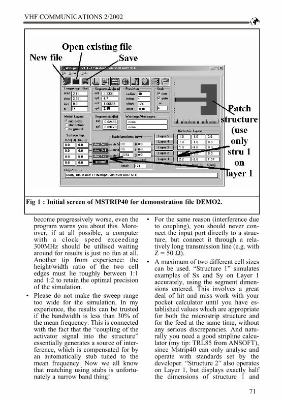
Fig 1 : Initial screen of MSTRIP40 for demonstration file DEMO2.
VHF COMMUNICATIONS 2/2002
71

must have it’s own drawing in thecircuit editor. It is then made congru-ent by entering a substitute with struc-ture 1. (See corresponding demo ex-amples).
3.Procedure using programMSTRIP40
3.1. InstallationFollowing download the programs anddata must be unzipped on the hard disc inthe usual way. It should be unzipped tothe directory C:\Mstrip40. In this newdirectory, we find all the necessary exefiles, together with two important fold-ers:• “mstrip40\data” contains all the simu-
lation examples supplied.• “mstrip40\ manual” has the operating
instructions and the online help.Before we start the program, we add anattractive icon to the Windows screen(You already know how: click on theright hand mouse button in an empty spot
on the screen, then “New link”, “Scan”,select “Mstrip40.exe”, open......etc.). Butwe still can't start the program. There issomething very important to do first.The newly unzipped “mstrip40.ini” filemust be copied into the C:\WINDOWSdirectory straight away. As a precaution,you should then open it immediately witha text editor and check and/or correct thesettings. Table 1 shows the correct andcomprehensive path settings for storageon hard disk C:\ in directory “mstrip40”with an automatic start up of example“DEMO2”. The path for the personalHTML editor in the fifth line may needaltering. Please check everything!
3.2. Demonstration of characteristicsand operation using example DEMO2Now we start up the program and weshould see Fig. 1. Unfortunately theblack and white text does not reflect theblaze of colour which welcomes you. InFig. 1 it is immediately clear that we cannot only start up a new project or store achange. Using the centre button, we canactually load the various examples di-rectly, a click brings up a long list ofstructure files with the suffix “str”. Wemake the selection by clicking on the
[Mstrip40]PathName=C:\Mstrip40\data\DEMO2,STRFileName=DEMO2.STREditorName=notepad.exeHtmlName=C:\Programme\Internet Explorer\IEXPLORE.EXE C:\mstrip40\manual\manual.htmProgramPath=C:\MSTRIP40\
[Ms_smith]PathNameC3d=C:\Mstrip40\data\DEMO2.slvFileNameC3d=Mstrip40\data\DEMO2.slv
[Current3D]PathNameC3d=C:\Mstrip40\data\DEMO2.slvFileNameC3d=Mstrip40\data\DEMO2.slv
[Pattern3D]PathNameC3d=C:\Mstrip40\data\DEMO2.slvFileNameC3d=Mstrip40\data\DEMO2.slv
Table 1 : Contents of the Mstrip40 control file Mstrip40.ini.
VHF COMMUNICATIONS 2/2002
72
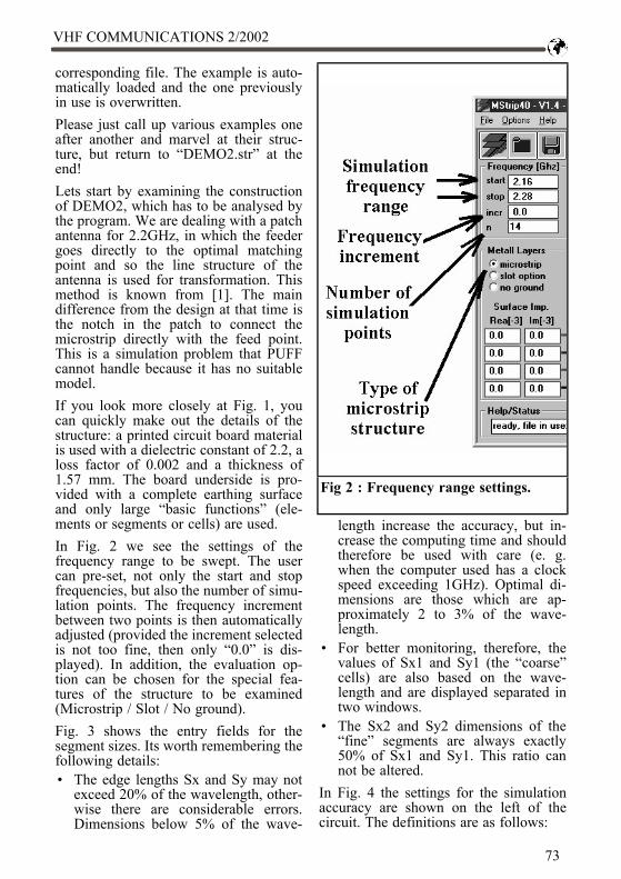
corresponding file. The example is auto-matically loaded and the one previouslyin use is overwritten.Please just call up various examples oneafter another and marvel at their struc-ture, but return to “DEMO2.str” at theend!Lets start by examining the constructionof DEMO2, which has to be analysed bythe program. We are dealing with a patchantenna for 2.2GHz, in which the feedergoes directly to the optimal matchingpoint and so the line structure of theantenna is used for transformation. Thismethod is known from [1]. The maindifference from the design at that time isthe notch in the patch to connect themicrostrip directly with the feed point.This is a simulation problem that PUFFcannot handle because it has no suitablemodel.If you look more closely at Fig. 1, youcan quickly make out the details of thestructure: a printed circuit board materialis used with a dielectric constant of 2.2, aloss factor of 0.002 and a thickness of1.57 mm. The board underside is pro-vided with a complete earthing surfaceand only large “basic functions” (ele-ments or segments or cells) are used.In Fig. 2 we see the settings of thefrequency range to be swept. The usercan pre-set, not only the start and stopfrequencies, but also the number of simu-lation points. The frequency incrementbetween two points is then automaticallyadjusted (provided the increment selectedis not too fine, then only “0.0” is dis-played). In addition, the evaluation op-tion can be chosen for the special fea-tures of the structure to be examined(Microstrip / Slot / No ground).Fig. 3 shows the entry fields for thesegment sizes. Its worth remembering thefollowing details:• The edge lengths Sx and Sy may not
exceed 20% of the wavelength, other-wise there are considerable errors.Dimensions below 5% of the wave-
length increase the accuracy, but in-crease the computing time and shouldtherefore be used with care (e. g.when the computer used has a clockspeed exceeding 1GHz). Optimal di-mensions are those which are ap-proximately 2 to 3% of the wave-length.
• For better monitoring, therefore, thevalues of Sx1 and Sy1 (the “coarse”cells) are also based on the wave-length and are displayed separated intwo windows.
• The Sx2 and Sy2 dimensions of the“fine” segments are always exactly50% of Sx1 and Sy1. This ratio cannot be altered.
In Fig. 4 the settings for the simulationaccuracy are shown on the left of thecircuit. The definitions are as follows:
Fig 2 : Frequency range settings.
VHF COMMUNICATIONS 2/2002
73

Fig 3 : Entering segment size information.
Fig 4 : Simulation precision settings and correction stub.
VHF COMMUNICATIONS 2/2002
74

• The “Precision Radius” determines(in the form of the number of seg-ments) the “range of reciprocal influ-encing and coupling” in a cell. On thispoint, the manual supplies the infor-mation that sufficiently precise resultscan be expected if this radius coverstwo-thirds of the structure to be inves-tigated.
• The “Integration Precision” factor isnominally 1 and lays down the nu-merical computing accuracy in solv-ing the reaction integrals. Only forextremely small or extremely largebasic functions or for very thick lay-ers can it be increased up to 5 (onceagain at the expense of computingtime).
Fig 5 :Structureexamined byDEMO2.
Fig 6 : Detailview of thestructure.
VHF COMMUNICATIONS 2/2002
75

• “Steps” indicates the number of basicfunctions to be processed. In eachcase, the number includes all theindividual segment edges present inthe X direction (here: 110) and thenumber of segment edges in the Ydirection (here: 64).
• “Error” gives the permissible residualerror for the calculation of such anintegral (Default: 1%). If it is under-shot, the program moves on to thenext basic function.
On the right hand side of the circuit thereis a stub option, this compensates forinput impedance errors caused by theinput signal. As soon as “Automatic” isactivated, the program automatically cor-rects this problem by connecting an openstub (not visible). But please rememberthat such compensation is narrow band,and heed the warnings in the manual(Page 11):• “Dont select frequency ranges which
are too big!”
• Leave sufficient distance between thecoupling port and the structure (usinga suitable feed line)!
Now can we pay closer attention toexample DEMO2.The antenna structure which can be seenon the right hand side is used only forrough information, the precise dimen-sions and a precise breakdown of thecells used can be seen by clicking on thebutton shown in Fig 5. This opens awindow, which can be zoomed, in thisway the precise structure can be exam-ined, see Fig. 6. Take a really close lookand you will see something nice: theprogram automatically breaks each cellup again into four equal sections, in orderto increase the accuracy of the simulationthis can be seen clearly as the cursor ismoved around. One last tip: the smallwhite box with the number “1” identifies“Port 1”, which is used to activate thestructure using the input signal.
Fig 7 : ASCII text file containing all of the simulation information.
VHF COMMUNICATIONS 2/2002
76

Very important:This display is only there to provideprecise information to the user and cannot be altered. All the details, togetherwith the type of structure or data entry,can be seen only if we press the buttonwith the pencil (it is directly to the left ofthe button just used). In Fig. 7 we can seethat, amazingly, everything is done withonly a simple ASCII file as used by anytext processing program! Its easy to seethe values transferred from the screeninput here for the frequency range beingexamined, the printed circuit board data,the segment dimensions and the structure1 selected for this project (largest seg-ments on layer 1). The selected entryform for the microstrip structure is espe-cially amusing, it is embedded in a fieldof dots (these form, so to speak, theprinted circuit board with the lowercontinuous earthing surface, i.e. the“ground” and can be imagined as goingon for ever). Each hash sign entered
represents a segment and the “1” at thebeginning of the feeder is naturally port 1for activating the structure.
A tip:Those wishing to experiment furthershould make life easier for themselvesand store the demo example under an-other name. Then open this structure fileand experiment by altering the valuesentered or the “drawing”. In this way,you can save yourself the trouble ofstarting a new file and keying in all thevariables required that would take up alot of time!If we now look at Fig. 8, we find thefunctions of all the remaining buttonsexplained. Anyone with a lot of time tospare can re-start the entire calculationusing the next button in the row (symbol:little computer) on relatively old comput-ers, this is an opportunity for an extendedcoffee break! It is interesting to print outthe Smith chart of the results (Fig. 9). As
Fig 8 : The function of remaining buttons.
VHF COMMUNICATIONS 2/2002
77
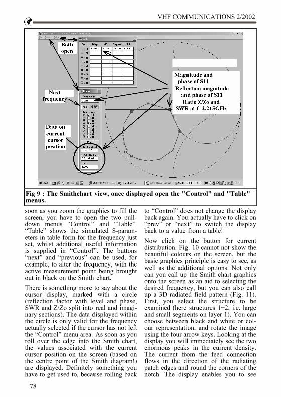
soon as you zoom the graphics to fill thescreen, you have to open the two pull-down menus “Control” and “Table”.“Table” shows the simulated S-param-eters in table form for the frequency justset, whilst additional useful informationis supplied in “Control”. The buttons“next” and “previous” can be used, forexample, to alter the frequency, with theactive measurement point being broughtout in black on the Smith chart.There is something more to say about thecursor display, marked with a circle(reflection factor with level and phase,SWR and Z/Zo split into real and imagi-nary sections). The data displayed withinthe circle is only valid for the frequencyactually selected if the cursor has not leftthe “Control” menu area. As soon as youroll over the edge into the Smith chart,the values associated with the currentcursor position on the screen (based onthe centre point of the Smith diagram!)are displayed. Definitely something youhave to get used to, because rolling back
to “Control” does not change the displayback again. You actually have to click on“prev” or “next” to switch the displayback to a value from a table!Now click on the button for currentdistribution. Fig. 10 cannot not show thebeautiful colours on the screen, but thebasic graphics principle is easy to see, aswell as the additional options. Not onlycan you call up the Smith chart graphicsonto the screen as an aid to selecting thedesired frequency, but you can also callup a 3D radiated field pattern (Fig. 11).First, you select the structure to beexamined (here structures 1+2, i.e. largeand small segments on layer 1). You canchoose between black and white or col-our representation, and rotate the imageusing the four arrow keys. Looking at thedisplay you will immediately see the twoenormous peaks in the current density.The current from the feed connectionflows in the direction of the radiatingpatch edges and round the corners of thenotch. The display enables you to see
Fig 9 : The Smithchart view, once displayed open the "Control" and "Table"menus.
VHF COMMUNICATIONS 2/2002
78

Fig 10 : Thecurrentdistribution atthe selectedfrequency.
Fig 11 : 3D view of the current distribution.
VHF COMMUNICATIONS 2/2002
79

Fig 12 : Radiation pattern view with information on antenna gain.
Fig 13 : 2Dview ofradiationpattern.
VHF COMMUNICATIONS 2/2002
80

exactly what happens.The next button brings us to the radiationpattern diagrams. Once the menu isopened, call up “Infos and Controls” andimmediately read off the prediction forthe antenna gain (Fig. 12) together withthe details of the 3D radiated field pat-tern. The four arrow keys can again beused for rotation i.e. the angle of obser-vation can be changed. But you shouldjust play about with the various simula-tion options (right up to cross polarisa-tion). To be honest, for individual menuitems you really need to look through themanual or look in the appropriate litera-ture in order to grasp the deeper mean-ing.
Incidentally:If you miss your beloved 2D directionaldiagram, click the option “2D Pattern”under “Kos”. Fig. 13 will then make youvery happy, since here too the angle ofobservation can be varied using the ar-
row keys.
3.3. My own example:Determining the data for a patch antennafor METEOSATAs a stimulation for your own work, thespecimen antenna from the article inVHF Communications [1] is to be simu-lated here using Mstrip40, to check howfar we are from the actual measurementtaken at the time. The material data are asfollows:• Printed circuit board material: Rogers
R04003• Relative permitivity: 3.38• Board thickness: 1.52mm• Dielectric loss factor tanδ: 0.001 at
1,600MHzThe patch created and investigated had awidth of 58.67mm and a length of46.48mm, this length giving precisely thefrequency of resonance of 1,691MHz(see simulation in Fig. 31 on Page 76 in
Fig 14 : Details of example entered into main input screen.
VHF COMMUNICATIONS 2/2002
81

Part 2 of the article referred to). For afeeder with Z=50 Ω, we need a micros-trip line with a width of 3.52 mm.
1st step:Open the specimen “DEMO1.str” andsave it using “SAVE AS”, giving it anew personal name.
2nd step:Enter the board data correctly, split thefrequency range from 1.5 to 2GHz into21 segments and adopt the precise widthof the 50Ω feeder (i.e. 3.52 mm) for thesegment dimension, Sy. Divide the radia-tor length of 46.48 mm into 10 equalsections, thus giving a value of Sx =4.648 mm.Very important: you must save every-thing immediately afterwards by “press-ing the key with the diskette”.Fig. 14 shows the screen with theseentries. Both the step width for thefrequency steps and the values of Sx andSy based on the wavelength are enteredautomatically. It can also be seen that therequirements listed at the beginning ofthis article (dimensions between 2% and4% of the wavelength, and no side ratioexceeding 1:2) are correctly fulfilled.
3rd step:Now open the circuit editor with thespecified button and look at the top halfof all the simulation objectives.The antenna is in the bottom half of thepage change the existing structure therewith the keyboard. In the horizontaldirection, enter 10 hash signs in each line(10 x 4.648 mm = 46.48 mm). There isan inaccuracy in the vertical direction, Sy= 3.52 mm and for a patch width of58.67 mm we would actually need 16.66segments. So we use 17 by filling 17lines with a hash signs. Finally, pleasedont forget the feeder (in line 9) and the“1” for the input port. Fig. 15 showswhat the result should look like.
4th step:First carefully save everything and thenclose the editor. Press the “key with thecomputer” to start the simulation and,following an appropriate compulsorycoffee break, call up the Smith chartgraphics for the S-parameters. After call-ing up “Control” and “Table” as well (aspreviously described), you should have agraphic similar to Fig. 16. The inputreflection loop, which is typical of patchantennas, is very easy to recognise, and
Fig 15 : View ofthe text filecontainingdetails of thestructure.
VHF COMMUNICATIONS 2/2002
82

Fig 16 : The first simulation shows the resonant frequency of the antennabetween 1725 and 1750MHz.
Fig 17 : The narrowband simulation show the resonant frequency of theantenna as 1735MHz and the radiation resistance as 282.5ΩΩΩΩ.
VHF COMMUNICATIONS 2/2002
83

you have only to look for the minimumof |S11| to find the natural resonance.According to the simulation, it lies some-where between 1.725 and 1.75 GHz andunfortunately the selected scale divisionis too coarse there. Consequently, we usea new simulation with a narrower fre-quency range of 1.700 to 1.750 GHz.Please dont forget to save the new entriesagain before starting the simulation onthe basis of my experience, it is perfectlyreasonable to open the editor files againand check whether everything has beencorrectly transferred. The program fre-quently develops an unexpected life of itsown and simply rejects such commands,but does not report this on the screen.Now and then, though, the messageflashes up that, if there are problems orcrashes, the two files “*.rea” and “*.slv”should be deleted from the specimendirectory with Explorer to make every-thing work correctly again.
5th step:In Fig. 17 we can see not only the resultof this narrowband simulation, but alsothe next action we have to take. We nowcall up the individual frequencies oneafter another and look for the smallestvalue of |S11|. This can be found at thefrequency f = 1,735MHz , where there isa minimum value of r=0.7. This can beused immediately, just roll the cursoralong the horizontal axis of the Smithchart from its centre point, moving rightuntil you reach the display “rho = 0.07”.The ratio of the real component to thesystem resistance is then automaticallydisplayed in the “Control” field as 5.65.The patch antenna consequently displaysa real input resistance of 50Ω x 5.65 =282.5 Ω at the feed point, since by thisaction we have simply “turned back” the50Ω feed line right up to the radiatingpatch edge. If you take another look atthe screen photo, Fig 28 on page 73 ofVHF Communications 2/2002, it showsthe network with its reflection factor ofprecisely 10% at the resonance point.Then do some calculations, you will
come up with an interesting result. Theactual radiation resistance at the feedpoint of the antenna is actually 20 %higher here than it was assumed to be. Ifthe start value selected for the simulationis 200Ω, in reality this would be 1.2 x200Ω = 240Ω - so were not all that faraway with the Mstrip40 simulation ofapproximately 280Ω. Thus the overallresult is entirely usable, even if Mstrip40also yields a self resonant frequency of1,735MHz instead of 1,691MHz (whichis just 3 % too high).One more interesting thing: If we nowrepeat the simulation with a shorter orlonger feeder, or with shorter or longertime measurements, then we are never-theless still faced with a result whichgives us a frequency of resonance ofbetween 1,720 and 1,750MHz and aninput resistance of between 250 and300Ω.
6th step:What would all this trouble be worthwithout the antenna gain? Correctly cal-culating the radiation characteristics iscertainly one of the most important prop-erties of Mstrip40. If you press the“Pattern key” in the main menu, and thenopen “Info and Control” and enter afrequency of 1,735MHz, you obtain theinformation “Gain = 6.6 dB”.You can then also analyse the 2D and 3Ddirectional diagrams in any way youwish, or check the current distribution onthe patch at the precise resonance.
3.4. SummaryMstrip40 only supplies really goodanalyses of the extremely diverse micros-trip and antenna structures if the proce-dures discussed are adhered to. Solidknowledge regarding the subject matteris indispensable here, not just with regardto the objects to be simulated, their mainbehavioural characteristics and the re-sults to be expected, but likewise withrespect to the characteristics and limita-tions of the EM simulators. Otherwise,
VHF COMMUNICATIONS 2/2002
84

the simulation result easily becomes alottery! Before beginning any work ofyour own, it is indispensable to carry outa very thorough analysis of all the speci-men programs and of the manual. This isthe only way to get to the bottom of themysteries of the simulation of normal andabnormal patch antennas, slit antennas,arrays, or any type of aperture-coupledstructures, etc. Who would have previ-ously suspected that, for example, theoption “no ground” could have been usedto simulate the main outlines of thebehaviour of microwave dipole antennasin the open air? All in all, this requires agreat deal of preparatory work, but it isrewarded with a considerably deeperunderstanding of the relationships in-volved and with usable preliminary plansfor a practical project.
4.Literature:
[1] Gunthard Kraus: “Modern Patch An-tenna Designs, Part 1 and Part 2”. VHFCommunications 1/2001 and 2/2001[2] Mstrip40 manual[3] SONNET-LITE manual[4] APLAC manual
VHF COMMUNICATIONS 2/2002
85

With over 1000 members world-wide, the UK Six Metre Group is the world’slargest organisation devoted to 50MHz. The ambition of the group, throughthe medium of its 60-page quarterly newsletter ‘Six News’ and through it’sweb site www.uksmg.org, is to provide the best information available on allaspects of the band: including DX news and reports,beacon news, propaga-tion & technical articles, six-metre equipment reviews, DXpedition news andtechnical articles.
Why not join the UKSMG and give us a try? For more information, contactthe secretary Iain Philipps G0RDI, 24 Acres End, Amersham, Buckingham-shire HP7 9DZ, UK or visit the web site.
The UK Six Metre Group
www.uksmg.org
VHF COMMUNICATIONS 2/2002
86

Even on its own, a digital speech storeis a practical aid, the project becomeseven more interesting if a sequencerand a “Roger peep” are integrated. Amicro controller is responsible for con-trolling the system, as in the originalversion [1].
1.Circuit description
The circuit diagram of the speech storewith the sequencer is shown in Fig. 1.The main elements of the speech storehave already been described in [1], sothey are merely summarised here.The IC ISD 2560 speech memory storesa maximum of 1 minutes speech and canplay this back as often as desired. Thecontents of the memory are still retainedeven if the power fails. When the changeover switch is operated, the systemchanges from recieve to playback, or viceversa. The external analogue wiring ofthe IC is for filter functions, and formatching the level to the microphoneinput of the transceiver.The complete control system, both forthe speech store module and to theexterior, through the sequencer is oper-ated by the AT90S2313-10PC microcontroller.
The integrated sequence control serves toguarantee when the transceiver, or anyadditional equipment, such as a poweramplifier or a masthead preamplifier, isswitched on or off.When the PTT key is activated, circuitoutputs A to D are activated in a pre-cisely co-ordinated timing sequence, andare de-activated again once the key isreleased. The power MOSFETs T1 to T4are used to provide suitable amplificationfor the switching signals which controlthe PTT connection of the transceiver,the power amplifier, the antenna relay,etc.The time cycle of 50ms, for the switch-ing sequence of the sequencer, is derivedfrom the crystal frequency (Q=5 MHz)through the software. The diagram inFig. 3 makes the time sequence of theswitching procedures clear.The microphone PTT key is connected toport PB7 of the micro controller (IC2,Pin 19).If desired, the function of a “Roger peep”can be selected through connections PB3and PB4. as follows:
Wolfgang Schneider, DJ8ES
Speech Store with IntegratedSequencer
Roger Pip PB4 PB3
no Jumper Jumperpip Jumper -cancelled Jumper"k" - -
VHF COMMUNICATIONS 2/2002
87

VHF COMMUNICATIONS 2/2002
88

The circuit also offers the option ofremotely powering an antenna amplifierthough the downlead or through a sepa-rate cable. An operating voltage of 12VDC is available for the masthead pre-amplifier to do this, by means of the T6(BD 135) transistor.The “all stations call” key at port PB6(IC2, Pin 18) of the micro controllerinitiates the transmission of an individualsequence, both for the initial reception ofthe “all stations call”, and for the play-back.The “all stations loop” key PB5 (IC2, Pin17) initiates an endless loop. By meansof a jumper, the pause length of 5, 10, 15or 20 seconds can be set between twocalls. In the intervals, the PTT connec-tion is always inactive and the trans-ceiver switches to reception.The “Stop” key PB4 (IC2, Pin 16)interrupts the endless loop or any othersequence. Thus an “all stations call” inprogress can be interrupted at any time.
The “Stop” key also activates the endingof speech input.
Fig 2 : Completed speech store in an aluminium case as produced by FrankPeter Richter, DL5HAT.
Fig 3 : Timing diagram showing thedisplacement of each signal.
VHF COMMUNICATIONS 2/2002
89

Fig 4 : PCB layout for the speech store.
Fig 5 : Ground plane side of PCB.
VHF COMMUNICATIONS 2/2002
90

Fig 6 : Component layout for the speech store.
Fig 7 : Layout of SMD components.
VHF COMMUNICATIONS 2/2002
91

2.Assembly instructions
The speech store with sequencer is as-sembled on a double sided copper coatedepoxy printed circuit board (Figs. 4 and5) with dimensions of 100 mm x 75 mm.The fully coated side is an earthingsurface. The earth connections are sol-dered in accordance with the componentsdrawing (Fig. 6).The two IC sockets and all the othercomponents, with the exception of thespeech store (IC1) and the micro-control-ler (IC2), are inserted and soldered inaccordance with the components draw-ing, Fig. 6.Mounting of the SMD components onthe foil side is shown in Fig. 7. Theinputs and outputs are fed using 1mmsolder studs. The selection of the delay(waiting time) and “all stations loop” canbe made by means of jumpers.The T6 (BD135) transistor should beinsulated, using a mica washer (and heatconducting paste).The micro controller and the speechmemory IC are not inserted until later on.First the function of the 5V voltageregulator is tested with a digital multim-eter. To do this, the supply voltage of+12V DC, or better 13.8V DC, is appliedand the stabilised voltage of +5V ismeasured at IC 1 (Pin 20) and IC 2 (Pin28). Only now can the two ICs beinserted into their bases.
2.1. Component list1 x Printed circuit board DJ8ES056IC1 ISD 2560, speech memory ICIC2 AT90S2313-10PC,
micro controllerIC3 78L05, voltage regulatorT1-T4 IRF830, power MOSFETT5BC548B, transistorT6BD135, transistorQ1 Crystal 5.0000 MHzR13,14 Trimmer 250Ω, RM 5/10mm,
horizontalR15 470Ω/0.6W, RM 10mmRN1 Resistance array 8x10kΩ1 x Loudspeaker 0.5W/8Ω1 x Electret microphone1 x LED red, low current1 x IC holder, 20pin1 x IC holder, 28pin1 x Post strip, 2x8pin1 x Heat sink PR-32/25,41 x Change over switch, 1pin,
On/On4 x Hand actuated auxiliary switch15x Soldering stud 1mmResistors 1/4W, RM 10mm:1 x 47Ω3 x 4.7kΩ2 x 1.5kΩ3 x 10kΩSMD resistors, 1206:R1 10kΩR3 470kΩR4 4.7kΩSMD capacitors:C1 10µ/25V; SMD tantalumC2 1µ/16V; SMD tantalumC3 4.7µF/16V; SMD tantalumC4,5 27pF, ceram. SMD 120611x 100nF, ceram. SMD 1206
3.Putting into operation
Once the circuit has been assembled, thefunctioning of the voltage regulatorchecked and the ICs inserted, the equip-ment can be put into operation.The waiting time for the “all stationsloop” and the audio level for the unit areset at trimmer R14 or R13 for the “Rogerpeep”. The audio output should drive thetransceiver to full output, but should justnot over modulate it (key word - band-width)! This audio output is appliedparallel to the microphone at the micro-phone jack of the transceiver.
VHF COMMUNICATIONS 2/2002
92

The current consumption of the unit with+12 V (13.8 V) supply, in the variousoperating conditions is as follows: zerosignal current 10mA, when PTT key ispressed 40mA and during an “all stationscall” and /or when “all stations loop” isactivated approximately 70mA.The sequencer is connected into themicrophone line. To do this, the PTT lineshould be modified. The PTT contact onthe microphone controls the circuit andthus ensures that the station componentsare switched on and off at the correcttimes. The control outputs can be wiredup, for example, as follows:
A Antenna relay and/or preamplifierB Power amplifierC TransverterD Transceiver
If you dont want to test the functioningof the sequencer in practical operationstraight away, you can initially wire upthe outputs A to D with light emittingdiodes (1kΩ to +12 V). The time se-
quence and thus the functioning of theswitching outputs is visible.In order to make and / or save an “allstations call”, proceed as follows:
• Switch in “Record” position
• Start recording using “all stationscall” key
• Speak text (all stations call) intomicrophone
• End recording using “Stop” keyThe LED lights during the recording.The maximum recording time is 1Minute.Note: In recording mode, no radio equip-ment should be connected, otherwise thetransceiver automatically switches totransmission through the PTT connectionwhen the “all stations call” key ispressed.In playback mode (switch in “Play”position) pressing the key can be selected
Fig 8 : Photograph of completed printed circuit board for the speech store.
VHF COMMUNICATIONS 2/2002
93

to bring about a single “all stations call”or an “all stations loop” (endless loop).The desired pause length between twocalls can be set individually:
During the pause, the PTT connectiongoes to “high” and the transceiverswitches to reception.The “Stop” key interrupts the endlessloop or other sequences.Finally, once again my sincere thanks toFrank Peter Richter, DL5HAT, for devel-oping and testing the software for thespeech memory with the integrated se-quencer and the “Roger peep”.
4.Literature references
[1] Wolfgang Schneider, DJ8ES: DigitalSpeech Memories for Radio Applica-tions, VHF Communications, issue2/2001 pp 87 - 91[2] Wolfgang Schneider, DJ8ES: Microcontrolled: Sequence Control (Se-quencer) with Roger Peep, Funkamateur49 (2000)
Fig 9 : Rear view of the completed unit.
Pause PB1 PB0
5sec Jumper -10sec Jumper -15sec - Jumper20sec - -
VHF COMMUNICATIONS 2/2002
94

The technical options for modern ra-dio equipment are mainly dependenton the circuit technology, antennasand the type of modulation. Otheressential factors are the signal-to-noiseratio and the selection of the appropri-ate transmission method.
1.Overview
The following article describes the tech-nical options for modern radio equipmentto give the greatest possible sensitivity. Ittakes in the influence of the antenna, thecircuit technology of the receiver, thetype of modulation and the decoding.Tips are given on the optimum design ofreception systems. The central focus ison the signal-to-noise ratio required forthe individual application. In addition,some relationships are pointed out in-volving the noise, the noise figure andthe signal-to-noise interval. Improve-ments are suggested that can be intro-duced using digital transmission meth-ods.One basic requirement for radio equip-ment is that the range should be as greatas possible, provided a specific transmit-ting power is maintained Thus only theantenna and the receiver are available foroptimisation.
Antennas have a maximum power levelthat can be transmitted to them, deter-mined by their positions and sizes and byany directional characteristic. The limitsare defined by costs and handling.For receivers, the sensitivity limits arepredominantly defined by the noise. Thislimit varies a good deal, depending onwhether analogue or digital modulation isused for data transmission. Using highquality components with good design ofamplifiers, frequency converters and fil-ters, and finally with good modulationmethods and error correction, sensitivitycan now be taken far beyond the previ-ous margins. This article is intended tooffer a general survey of the current stateof the art.
2.Antenna equipment
Depending on the operating range, radioantennas can take widely varying forms.Receiving equipment for signals fromspace ranges from the 60cm dish forsatellite reception all the way to the radiotelescope with a diameter of 100m. Roofantennas for VHF and television recep-tion are also widespread.Then there are the tiny rod or flat topantennas in mobile telephones, as well asthe considerably larger antennas on the
Prof. Gisbert Glasmachers
The Sensitivity of RadioEquipment
VHF COMMUNICATIONS 2/2002
95

radio masts of base stations. Here too, thegeneral rule is that the reception fieldstrength available must be converted intoas high an antenna power level as possi-ble. There are basically several optionsavailable for bringing this about [1],[2]:The antenna should be as big as possibleA large antenna can pick up more powerfrom the electromagnetic field than asmall one. Consequently, a large antennaincreases the sensitivity of the receptionequipment.One absolutely classic example is thecombination of the mobile telephone andthe base station. Both pieces of apparatusare designed in such a way that they haveapproximately the same range duringtransmission and reception, and thus alsohave the same limiting sensitivity. Theratio of the transmission power levelshere varies very widely, the base stationhas a transmission power level about 100times that of the mobile phone. Moreoverits antenna is much larger than that of themobile. The base station needs a hightransmission power level because themobile telephone, with its tiny antenna,can not receive much power. The basestation also needs a large antenna inorder to receive the weak signals fromthe mobile phone. In this case, the limitsare determined by peoples comfort. Themobile must be small, because its userwould not accept a large antenna.The antenna should have a directionalcharacteristicParaboloidal reflector antennas have astrong directional characteristic. This ef-fect can easily be observed when asatellite dish is being aligned. The signalsfrom the satellite itself cover an areatotalling millions of square kilometers inall. However, its signals are receivedonly if the dish is accurately aligned withthe satellite.If transmitters and receivers neverchange their location, this means thesensitivity can be increased many timesover, as opposed to a simple “all round
reception”. It is also easier to tune outany sources of interference.Even if such ideal pre-conditions are notpresent, it is sensible to use a directionalcharacteristic. We can thus make sure,even for mobile telephones, that as littlepower as possible is emitted directly intothe head of the telephone user. The majorlobe points in the opposite direction, sothat any possible biological damage iskept as slight as possible.The antenna must be optimally matchedto the receiverThe impedance at the connection point ofthe antenna must be resistive, in order toguarantee an optimal connection to thereceiver’s feeder. Any reflection reducesthe available power at the receiver input.Since antennas often have a markedfrequency response, the phase angle ofthe impedance is only relatively small inthe vicinity of resonance. In other words,the antenna should be carefully tuned tothe transmission frequency. This expenseis worthwhile for systems with a narrowfrequency range, in particular, such as,for example, on the bands licensed forgeneral purposes at 433 MHz and 869MHz.The difference in range between a sec-tion of “thrown out wire” and a carefullytuned and directed antenna is consider-able.
3.The signal-to-noise ratio
The heterodyne principle is nowadays inuse practically everywhere. Whether sin-gle or double conversion is involved haslittle to do with the sensitivity. Thedeciding pre-conditions for high sensitiv-ity are laid down in the input stage beforethe first mixer.The variable that limits everything is thesignal-to-noise ratio (S/N). This ratio can
VHF COMMUNICATIONS 2/2002
96

become progressively lower, and thusworse, during the passage through thevarious stages of a receiver. Pre-amplifi-ers (LNA), filters, mixing stages andlocal oscillators are decisive for a suffi-ciently high receiver S/N. The S/Nshould be pre-set initially [3]:The definition of the S/N is based on acomparison between the signal powerand the noise power:
In general, both the signal power and thenoise level are functions of the fre-quency.A generally recognised example of asignal is human speech. It encompasses afrequency range between approximately50Hz and 10kHz. The intensity withinthis spectrum is variable. In addition,there are variations between men andwomen, children and adults, soft speechand loud shouting. Because in thesecircumstances we can not arrive at auniform definition, we usually preferinstead to take one or more pure sinusoi-dal oscillations with a precisely definedamplitude as a signal, especially for thepurposes of measurement.Noise is also a variable distributed overthe frequency range. An output uni-
formly distributed over the entire fre-quency range is described as “whitenoise”. Fig. 1 shows, in simplified form,the spectrum distribution of a speechsignal and the noise on the frequencyaxis. The area below the curve in ques-tion provides a measure of the output.The interference to a speech or musictransmission is considered to be mainlydependant on the signal-to-noise ratio.For a telephone connection on the marginof comprehensibility, a level of about10dB must be attained. That means thatthe signal level must be 10 times higherthan the noise level. For an acceptabletelevision image, we need 45dB. Forradio transmissions in stereo with hi-fiquality, we need 60dB. CD players givevalues of over 80dB. The parameters foracoustic and visual reproduction systemsare thus defined.
4.The noise figure
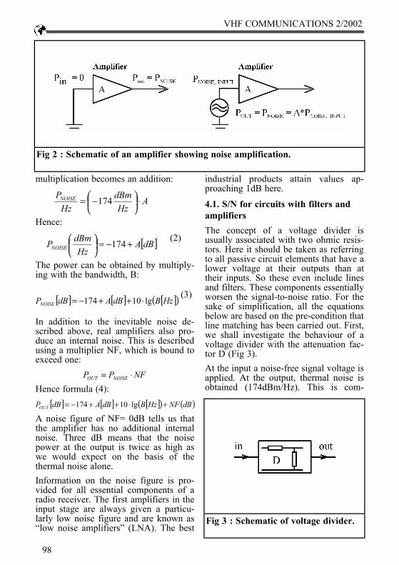
Electronic equipment such as amplifiers,mixers and demodulators essentially gen-erate a noise power at their outputs. Thisbehaviour is described as the noise figure(NF). For definition, the reference valueof the noise power is a passive dipole,e.g. an ohmic resistor. At room tempera-ture, it generates an available noisepower density of 174dBm/Hz. This valueis determined on the basis of physicalprinciples. We speak of “thermal noise”or “white noise”, because the origins liein the kinetic energy of the atoms, whichincreases in direct proportion to thetemperature. Essentially, a noise sourceof this type exists in every electroniccomponent.The model of an amplifier includes avirtual noise source at the input. Theamplified input noise then appears at theoutput - see Fig. 2.With logarithmic scaling, e.g.. in dB, the
NOISE
SIG
PP
NS = (1)
Fig 1 : Spectral distribution ofspeech and the white noise.
VHF COMMUNICATIONS 2/2002
97
multiplication becomes an addition:
Hence:
The power can be obtained by multiply-ing with the bandwidth, B:
In addition to the inevitable noise de-scribed above, real amplifiers also pro-duce an internal noise. This is describedusing a multiplier NF, which is bound toexceed one:
Hence formula (4):
A noise figure of NF= 0dB tells us thatthe amplifier has no additional internalnoise. Three dB means that the noisepower at the output is twice as high aswe would expect on the basis of thethermal noise alone.Information on the noise figure is pro-vided for all essential components of aradio receiver. The first amplifiers in theinput stage are always given a particu-larly low noise figure and are known as“low noise amplifiers” (LNA). The best
industrial products attain values ap-proaching 1dB here.
4.1. S/N for circuits with filters andamplifiersThe concept of a voltage divider isusually associated with two ohmic resis-tors. Here it should be taken as referringto all passive circuit elements that have alower voltage at their outputs than attheir inputs. So these even include linesand filters. These components essentiallyworsen the signal-to-noise ratio. For thesake of simplification, all the equationsbelow are based on the pre-condition thatline matching has been carried out. First,we shall investigate the behaviour of avoltage divider with the attenuation fac-tor D (Fig 3).At the input a noise-free signal voltage isapplied. At the output, thermal noise isobtained (174dBm/Hz). This is com-
Fig 2 : Schematic of an amplifier showing noise amplification.
AHzdBm
HzPNOISE ⋅
−= 174
[ ]dBAHzdBmPNOISE +−=
174
(2)
[ ] [ ] [ ]( )HzBdBAdBPNOISE lg10174 ⋅++−=(3)
NFPP NOISEOUT ⋅=
[ ] [ ] [ ]( ) ( )dBNFHzBdBAdBPOUT +⋅++−= lg10174
Fig 3 : Schematic of voltage divider.
VHF COMMUNICATIONS 2/2002
98

pletely independent of the attenuationfactor D. So if there is a signal-to--noiseratio of S/N1[dB] at the input of thevoltage divider, then there is a worsevalue of:
at the output. The reduction in the signal-to-noise ratio becomes particularly rel-evant in the input stage of radio receiv-ers, where the level is often not muchhigher than the thermal noise. Two cir-cuit variants can be found in practise -see Fig. 4. On the left is the band filterbefore the LNA, and on the right it isafter it.Let us assume that a noise-free signal isapplied at the input. Because some of thefollowing equations include addition andmultiplication or division, they can notbe written in logarithmic form (in dB).The amplification and the attenuationmust then generally be defined for out-put. The signal-to- noise ratio S/N for theleft-hand circuits can then be determinedas:
As can be seen, the amplification factorhas no influence on the S/N in theleft-hand circuit. On the other hand, theattenuation, D, of the filter and the noise
figure, NF, do have a negative effect. Sowe must make sure that filters with aslittle insertion attenuation as possible areused. For SAW filters, this is usually in arange between -2 and -5dB. In the right-hand circuit, we obtain:
For a high amplification factor A, apractical approximation can be obtained:
In this case, the negative influence of theattenuator is absent. The right-hand cir-cuit is therefore better than the left-handone. A more precise analysis can beobtained if the two equations (6) and (7)are cross-divided:
From this result, the factor can be deter-mined by which the two S/N valuesdiffer. A plausible numerical exampleshould make the difference clear:D = -3dB, A = 18dB, NF = 2.5dBThe S/N for the left-hand circuit is then
[ ] [ ] [ ]dBDdBNSdB
NS +
=
12
(5)
Fig 4 : Two methods of using a bandpass filter.
NFBHzdBm
DPNS SIG
LEFT ⋅
⋅−
⋅=
174
(6)
( )DANFBHzdBm
DAPNS SIG
RIGHT ⋅⋅+⋅
⋅−
⋅⋅=
1174
(7)
NFBHzdBmP
NS SIG
RIGHT ⋅
⋅−
=
174
(8)
DANF
NSNS
RIGHT
LEFT +⋅
=
1(9)
VHF COMMUNICATIONS 2/2002
99

only about half as large as that for theright-hand circuit, i.e. 3 dB worse. Natu-rally, other arguments can be put forwardin favour of the left-hand circuit. It isbetter protected against powerful externaltransmitters outside its own frequencyband.
4.2. The mixing stageTo change the frequency into the inter-mediate frequency, a mixer and a localoscillator are used. The most importantfactor is that the mixer has a considerableinfluence on the signal-to-noise ratio. Inprinciple, switched multipliers have con-siderably worse noise figures than alinear amplifier. Normal values are be-tween 10 and 18dB. In simplified termswe can use network of two elementaryamplifiers - see Fig. 5.The first amplifier represents the LNAand the second the mixer stage. The twohave different amplification levels (A1,A2) and noise figures (NF1, NF2). Theattenuation of the filters is likewise leftout of consideration here, as is theconversion to another frequency. For thisconfiguration, we have the followingsignal-to-noise ratio at the output:
One general requirement for a radioreceiver is that the stages after the pre-amplifier should not make the signal-to-noise ratio any worse. If this require-
ment could be completely met, we wouldobtain:
To make the result of equation (10) asclose as possible to that from equation(11), the following approximation mustbe fulfilled:
To put it in words, the amplification ofthe LNA must be considerably higherthan the noise figure of the mixer. This isa problem with many standard receiverdesigns where the two figures are of thesame order. If the insertion attenuation ofone or more filters is then added in, themixer stage, with its poor noise figure,frequently determines the actual signal-to-noise ratio of a receiver.To remedy this, the LNA should be twostages, so that an effective amplificationof at least 25dB is present before themixer stage.The local oscillator introduces an addi-tional requirement. The mixer amplifica-tion is linearly dependent on the level ofthis oscillator. This should therefore havethe highest permissible limit. In thestandard commercial mixers, this is atleast 10dBm. Integrated oscillators usu-ally attain a level of only 0 to approxi-mately 5dBm. In these cases, an ampli-fier between the oscillator and the mixeris very definitely recommended. Other-wise the mixer amplification could easilybe less than one. Then, in certain circum-stances, the intermediate-frequency am-plifier would also have a considerableinfluence on the signal-to-noise ratio.
4.3. The intermediate-frequencyamplifierThe considerations applying to the mixerstage are also valid for intermediate-frequency amplifiers. Their noise figuresmust therefore be lower than the productof the pre-amplification and the mixer
Fig 5 : Schematic showing the use oftwo amplifiers.
[ ]112
1
1174 NFANFBHzdBm
APNS SIG
⋅+⋅⋅
⋅−
⋅= (10)
1174 NFBHzdBmP
NS SIG
⋅
⋅−
= (11)
21 NFA >> (12)
VHF COMMUNICATIONS 2/2002
100

amplification. This condition can easilybe fulfilled using a respectable receiverdesign. Many integrated intermediate-frequency amplifiers have an AGC func-tion and/or a limiter, which an automaticamplifier regulator (AGC automatic gaincontrol) and amplitude limitation.Today the medium wave no longer playsmuch of a role on radio. Because itsamplitude modulation is subject to somuch interference, those using VHF haveconverted to frequency modulation. Butanalogue television also still has ampli-tude modulation. More modern systemsrely entirely on frequency or phasemodulation.But there are also quite a few standardsfor digital modulation, e.g. QPSK, whichalter both the frequency and the ampli-tude. These variations should be takeninto account when selecting the interme-diate-frequency amplifier. A limiter isincompatible with any type of amplitudemodulation. The time constant for theAGC must be set in such a way that theregulation system adjusts fast enough toa different signal level, without modify-ing the modulation to a significant extent.All types of modulation with constantamplitude, for example FM, MSK andGMSK, are free from all these problems.So at low signal-to-noise ratios these stilllead to acceptable results. The limitershould ensure that the amplitude is re-stricted to a maximum value at all levels.Amplifiers of this type will now beconsidered in greater detail.
Many integrated intermediate-frequencyamplifiers are manufactured as two-stageunits - see Fig. 6. A band filter can bewired up between connections 2 and 3.The total A1*A2 amplification attainsabout 90dB. The output voltage at termi-nal 4 is typically 200mVss. For thecalculations below, the following datahave been selected:
• Pre-amplification with mixeramplification 30dB
• Intermediate-frequency amplification90dB
• Intermediate-frequency band width100kHz
• Effective noise figure 6dBThe effective noise figure takes intoaccount the influence of the mixer andthe intermediate-frequency amplifier onthe total noise. Thus we obtain a level of+2dBm before the mixer. This is practi-cally sufficient to control the limiter, onthe basis of the noise output alone. Thereceiver apparently delivers a signal, al-though no antenna is connected. Since aneffective signal even if it should be athousand times more powerful than thenoise - also appears to lead to the samevoltage curve at the limiter output, thesignal-to--noise ratio can no longer bedetected at the limiter output. Meaningfulmeasurements can not be carried outagain until demodulation has taken place.Based on these considerations, we can
Fig 6 : Tow stageamplifier with alimiter.
VHF COMMUNICATIONS 2/2002
101

also find the limits at which we can stillobtain a meaningful value for the inter-mediate-frequency amplification. In theideal case, the amplification should be soslight that the thermal noise can not drivethe limiter all the way to its limits. Inaddition, the signal amplitude should beso high that the limiter always restrictsthe level. To make sure that if the signalis too weak, or is not present, the noise isnot received instead of the signal, manyintermediate-frequency amplifiers havean output that gives a voltage levelproportional to the level of the inputsignal. A threshold value can be set foran input power that is still acceptable.Below this threshold, the receiver willnot operate. This function is carried outon all mobile telephones.If the signal-to-noise ratio at the demodu-lator output is analysed, it is consideredin a different way. By “signal” in thepre-amplifier or the intermediate-fre-quency amplifier, we understand thepower of the entire spectrum, i.e. thecarrier and the sidebands. In the demodu-lator, only the energy of one or twosidebands is evaluated. The signal poweris thus considerably reduced. In addition,conversion losses are also involved. Thedegree of modulation likewise has aninfluence. On the whole it can be shownthat a demodulator considerably reducesthe signal-to-noise ratio.
5.Digital data transmission bymeans of radio systems
In the above analysis, the signal-to-noiseratio at the output is decisive for theefficiency of the receiver. We have al-ready referred earlier to how high itshould be for analogue radio and televi-sion applications.Modern systems predominantly rely ondigital transmission, even for speech and
images. The “poor sound quality” onradio when the signal-to-noise ratio islow is reflected in an increased bit errorrate (BER) in digital systems. On thissubject, here is a somewhat simplifiedexample from MSK: a signal-to-noiseratio of 0dB is assumed, with the signaloutput being exactly the same as thenoise output. On average, there will thenbe an error in every tenth bit. Even if thesignal power is only doubled (S/N =3dB) the ratio improves to give an errorin every fifty-first bit.A further advantage of digital systemslies in the fact that bit errors can becorrected to a certain degree. There areerror-correcting codes e.g. the Hammingcode - which, under certain conditions,can eliminate all bit errors[4].
6.Decoding
With analogue systems, we receive theoutput signal after demodulation. True, itthen has to be re-amplified in order, forexample, to be easily audible through aloudspeaker, but this amplification nolonger reduces the signal-to-noise ratio.The situation is different with digitalsystems. Here demodulation is followedby decoding, which turns the outputsignal back into a genuine digital signal.The lower the signal-to-noise ratio is atthe decoder input, the more bit errors itwill cause. However, decoders with ahigh level of efficiency can be assembledby means of ingenious techniques. Theseare in a position to decode digital signals,largely free from errors, even with a lowsignal-to-noise ratio. We might mentionthe matched filter technique and cross-correlation. There follows a brief de-scription of these two methods [5]:
6.1. Matched filter techniqueTo restrict the bandwidth, digital signalsare filtered before transmission along a
VHF COMMUNICATIONS 2/2002
102

radio path. Instead of square wavepulses, this gives rise to other forms withgentle flanks. These are digitised in thereceiver by means of scanning. In thematched filter method, the form of thetransmission pulse and the filter functionin the receiver are combined in such away that the correct value can be de-tected, with a high degree of probability,with a single scan of each bit (the choiceis only zero or one!). Relatively littletechnical effort is required.
6.2. Cross-correlationWith cross-correlation, the receiverforms the data itself, as if it were thetransmitter. But because it does not knowand can not know in advance whether azero or a one will be transmitted at anygiven moment, it forms both valuessimultaneously and keeps them ready intwo register banks. When the transmis-sion signals arrive hit, the receiverchecks, using a special algorithm, cross-correlation, whether the bit transmitted ismore like a one or more like a zero. Thisthen forms the basis for the digitaldecision. The method makes it possibleto extract signals, even when buried deepunder the noise. Even with an S/Nconsiderably below zero dB, good resultscan still be obtained. This is an enormousstep forward, when compared with allanalogue systems.The disadvantage lies in the high-levelcircuitry required. Cross-correlation canbe implemented in real time only withvery efficient field-programmable gatearrays (FPGA).
7.Data compression
A basic disadvantage of digital systemsis their requirement for increased band-width. It has already been pointed outthat human speech has a bandwidth ofapproximately 10kHz. But digitised
speech signals display a much higherbandwidth, which for average quality liesat about 100kBit/sec. The increasedbandwidth puts an unnecessary strain onthe expensive frequency bands in radiosystems, and thus increases the noisepower of amplifiers. This leads to a lot ofexpenditure to reduce bandwidths. Withmobile telephones, the effective band-width is restricted to about 23kBit/sec.The key phrase here is data compression.Thus redundant (i.e. superfluous) infor-mation is removed from the signal andonly the absolutely essential data aretransmitted. But on the receiver side thesignal must be converted back into itsoriginal condition (as far as possible).Data compression does not function un-der strict real-time conditions. The com-pressed signal is created only some timeafter the original signal. For transmis-sions between a transmitter and a re-ceiver without talkback, this delay causesno problems. It becomes more difficultespecially with a high degree of com-pression if two people are carrying on alive conversation. Further progressshould be expected in the future in thefield of data compression [6].
8.Outlook
The world of wireless telecommunica-tions has experienced an enormous up-swing, thanks to modern techniques incombination with digital data transmis-sion. Even radio amateurs can profit fromthis. Many circuits can be obtained atfavourable prices, and many can even beacquired free of charge as samples. It isalso worthwhile for the committed radioamateur to gain a wider understanding ofthe world of modern radio technologythrough his/her own experience.
VHF COMMUNICATIONS 2/2002
103

9.Literature
[1] Freyer, Ulrich, News TransmissionTechnology, Hanser-Verlag[2] Zinke/Brunswig, High-frequency En-gineering, Springer-Verlag
[3] Mildenberger, Otto, Essential Infor-mation Technology, Vieweg-Verlag[4] Bossert, Martin, Channel Coding,Teubner-Verlag[5] von Grüningen, Daniel, Digital Sig-nal Processing, Fachbuchverlag Leipzig[6] Zölzer, Udo, Digital Audio-signalProcessing, Teubner-Verlag
VHF CommunicationsBlue Binders
• Attractive blue plastic• Holds 12 issues (three years)• Allows you to find required issue easily• Will keep the XYL happy• £6.50 + shipping (UK £0.75, Surface £1.25, Air £3.00)
VHF COMMUNICATIONS 2/2002
104

1.Introduction
Since I have built a detector using thenew and interesting Logarithmic Detec-tor ICs from Analog Devices (AD8307and AD8313 [1]) I realised that the samedetector could be used directly in a noisefigure meter. This is because subtractingthe logarithms of signals is the same asdividing them by each other.I believe that there are at least twoshortcomings of this instrument, as de-scribed, but it works so well that I do notthink it matters too much.The detector does not treat the noisesignals as True RMS , but as Averages,introducing a small error.The detector does not have a zero outputfor a zero input signal. A small offseterror is introduced, but it can be trimmed.
2.Construction
The Logarithmic Detector IC (AD8307)and a dual OP amplifier (LT1630) foroffset and scaling of the signal and a 5Vregulator are assembled as per the sche-
matic diagram in Fig 1. These detectorsrun on 5V (LM78L05) but the rest of thecircuit is a ±12 or ±15V design. It isprobably not necessary to point out to theVHF Communications readers that thetwo 1 nF capacitors and the 10Ω resistorsare to be close to their pins on thepackage of the AD8307 (or AD8313).The LT1630 is a very good dual OP-amp, bipolar, “rail to rail” on both inputsand output. I prefer the LM78L05 regula-tor because it, as well as the OP, canhandle 32 volt, so make the capacitor onthe input a 35V one if you want to usethis detector as the “General Purpose”,free standing and very useful instrumentit is. It is my design, and it is trade-marked, registered with the U.S. PatentOffice, as LogProbe so should you feellike entering a commercial arrangementusing this, please let me know! I amagreeable!With the values shown (24k and 56k) theoutput will be very close to 10 dB/Volt.The 10k/1k1 sets the output DC level,and the “bottom” of this ladder may be a2 - 5k trimpot. The 47Ω on the output isto avoid capacitive loading of the OP. Itis a pretty fast one, the LT1632 is evenfaster, and it can handle some capaci-tance, but this way there will be noproblems. Besides, it may survive longshort circuits of the output.A noise source is constructed. This isdone best using a noise diode from the
Carl G. Lodström,KQ6AX & SM6MOM
A Simple Noise Figure Meter
VHF COMMUNICATIONS 2/2002
105

people who know how to make them [2]but I seem to have had good luck with aUHF transistor. Using the B-E junctionin reverse forms a Zener diode at about6v. Just as it turns on; it has a very nicenoise! Measure up “your” diode and beaware of that the noise level can changedramatically with just a few tenths of avolt supply variation! Maybe a constantcurrent (in the 10µA region) is the wayto drive them, I have not ventured intothis area. I tune the trimpot for maxsmoke. Although regular Zener diodes(above some 5-6V) seem to give plentyof noise of varying intensities, but theyfall flat above HF bands, some 30MHz,probably due to high internal capaci-tances. After all, they are designed tokeep a voltage stable and to handle asmuch current as possible.The schematic diagram of the noisesource is shown in Fig 2. It can, orshould, be enhanced regarding A1 outputrise and fall times as well as limiting thevoltage swing on the noise diode to aminimum. One may also contemplatestabilizing of the “On-voltage” since itcan be pretty sensitive. The switches onthe meters switch in different ranges of
sensitivity. The signals from a radioreceiver may be much stronger than froma 10dB LNA.Using the “Alt. In” (MAX4527 pin 7instead of pin 6) will switch whichcapacitor stores the S and which storesthe (S+N), reversing the M2 reading. IfM2 is offset (for example by means ofmaking the Reference input of the A3negative) to zero, the NF reading wouldgo “the right way”, showing 0 for 0 dBand more for larger NF values. Thenon-inverting input of A2 would thenhave to be connected to the other of thetwo electrolytic capacitors.The output of the noise source is passedthrough a 20dB attenuator [3], of thesurface mount “wind mill” type, thisensures a very good S11 on the source.Theoretically < 40dB return loss, but inreality depending on how accurate to50Ω the attenuator is, probably betterthan a RL of 36 dB.In the design of the chopped noisesource, it is a good idea (that I have notyet achieved) to see to that the DC on theoutput does not vary more than neces-sary. In other words: do not put the
Fig 1 : Schematic diagram of logarithmic detector.
VHF COMMUNICATIONS 2/2002
106

whole 0-6v on/off waveform on theattenuator! The noise may be totally offat 5.7V and on at 5.9V! Measure this anddo not apply (or turn off) more DC thanyou need for to turn the source on andoff. It may also be a good idea to use theA1 amplifier for this, even if the pin 3 onthe 555 has plenty of signal. The extraamplifier is there anyway. A voltagedivider with a permanent voltage, towhich is added or subtracted a little bythe square wave, should be easy to makeusing the A1. One can add R and C toslew the output ramps a little, whereasthe 555 has a very fast transient turn-onand turn-off. When you measure a re-ceiver you do not want any spikes likethese on the antenna input. It may well begood to make a 10µs rise and fall time onthe DC that is pulsing the noise source.That is a very small part of a period of16Hz anyway. In combination with theDC variation being kept to a minimum,this works very well on receivers. On an
LNA for UHF it would not matter eitherway.A simple oscillator that turns the noisesource on and off (slowly, <100Hz) isconstructed. Although I am not a big fanof the “555”, a circuit that may create asmany problems as it solves, here is agood place for it. The newer “CMOS-555” ought to work as well. As will anyother square wave generator. The versionI built here has the duty cycle (D.C.)adjustable widely around 50%, but this isprobably not necessary. Anything from20 - 80% is likely to work.
3.Function
A logarithmic detector converts AC (orDC) input signals to a DC signal that is
Fig 2 : Schematic diagram of the noise source.
VHF COMMUNICATIONS 2/2002
107
proportional to the logarithm of the inputsignal level. For AD8307 this is truefrom about 50µV to about 2.2V (differ-ential input) over a frequency range tonearly 1GHz. A 92dB range with verygood linearity and temperature compen-sation, quite good! The AD8313 has alesser range, some 70dB, but goes to2.5GHz.With a dual OP amplifier the DC detectoroutput, corresponding to the logarithm ofthe signal amplitude, can be shifted andscaled as one desires.The noise source is turned on and off at arelatively slow speed (it happened to be16Hz in my version). It is fed to thereceiver or Low Noise Amplifier undertest. The Logarithmic Detector is placedon the output of the amplifier (or re-ceiver). The signal from the detector isthus a DC voltage that alternates instrength, corresponding to log (S) andlog (S+N).The S/(S+N) is a measure of the sensitiv-ity of the device. Since the signals arepresent in their logarithmic form, one canperform the division by subtracting them!Using an analogue switch, synchronousto the 16Hz noise switching, the signalsare stored in either of two large capaci-tors. A resistor in series with he commonline makes sure the display is nice andsmooth, letting the capacitor voltage av-erage out over a few cycles of switching!The signals are subtracted in an Instru-mentation Amplifier with a gain of 1.The signal from this is the “Noise FigureSignal” and it is rather “1 NF” so tospeak. A reading on this M2 meter willbe identical to the other meter (the M1Gain meter) if a device is perfect, addingno noise of its own. Connecting thedetector directly to the noise source forexample. The lower the display of theM2 NF meter (compared to the value ofthe M1 Gain meter), the larger (worse)the NF of the device.The output to the M1, the Gain reading,is simply the voltage of the applied noise,
as amplified by the LNA (or receiver)and as detected by the logarithmic detec-tor.
4.Applications
The pulsating Noise Source is connectedto the input of a LNA (or receiver or anyother device under test) and the Detectoto its output. The LNA is (usually)tweaked for best NF and as good a gainas possible. To get an idea of “where itis”, connect the detector directly to thenoise source and note the readings. Ifthey are not equal, it is most likelybecause the detector has a little outputeven for no input signal. Adjust the 1k1in the detector schematic diagram! Con-nect again to the LNA!To see how much difference a changeNF reading makes, connect an attenuatorof 1 or 2dB and see “how much more”M2 drops when the NF is worsened bythe amount of the attenuator. This showsthe slope of the meter.For a sanity test, connect an attenuator tothe output to see the gain worsened bythe same amount as the attenuator value.If the attenuator is <10dB (or so) the NFreading should barely be affected. If theattenuator is connected to the input, bothM1 and M2 should drop by the sameamount This is a serious test of theinstrument!When connected to a radio one canactually “listen” to the audio with thelogarithmic detector! Be careful if con-nected to the loudspeaker output not toturn up the volume too much, and becareful about pops and clicks that maykill the detector. Personally I use a small1:1 audio transformer, mounted on a ¼inch audio plug, with a centre tap on thesecondary. I connect this tap to groundwith an electrolytic capacitor because theinputs of the Logarithmic Detector like to
VHF COMMUNICATIONS 2/2002
108

float around at a few volts. The IC worksfrom 2 to 5V common mode, but in thiscase there is no reason to steer them toany particular DC voltage. A couple ofcrossed diodes (1N4004 or similar)across the transformer primary may be avery good idea! They can pay for them-selves sooner than you think! A taperecorder output is safer to use, andfurthermore independent of the volumecontrol setting.The receiver has almost certainly AGC,which should be disabled for true meas-urements, but it may very well workanyway, especially on low input levels.One can also speed up the chopping ratea bit (make it variable!) to 50Hz or so,where the AGC is not fast enough tomake much difference. It is most interest-ing to take a look at the Gain and NF of a“General Coverage Receiver” to see howboth vary over any one band and fromband to band! That wonderful receiver issuddenly not so wonderful anymore,even though it still works fine!
5.FM receivers
FM receivers are limited in the IF so nomatter what strength of the input noisesignal, the audio (noise) will be thesame! So, the Logarithmic Detector hasto be used to pick up either the RF signalafter the front LNA or the IF after themixer, before the signal reaches thelimiter. Put a small coil between theinputs of the IC and “sniff” around forreadings on the Gain meter! The detectoris very sensitive and you can most likelyfind enough signals. Then: just trim theLNA for the best Gain/NF combinationas usual!
6.Example readings
Fig 3 shows measurment on a 2m LNA.
Fig 3 : Example reading testing a 2m LNA using a BF998 dual gate MOSFET.
VHF COMMUNICATIONS 2/2002
109

The readings on the Y axis are arbitraryreadings of the meters (identical) M1 andM2 numbers but the X axis shows theactual settings in dB of the attenuator. Asexpected, when the gain reading is inde-pendent if the attenuator is placed on theinput or the output (the upper twographs). For the “1-NF” reading, thelower two graphs show the reading drop-ping at once with the attenuator on theinput and at about 10dB when placed onthe input. This is the ultimate test of aninstrument like this, and a proof of itsfunction. It is likely that the LNA has aNF of a dB or two. If so, the noise outputfrom the source is ~12db ENR (Exces-sive Noise Ratio). This means 12dBmore than the thermal noise from a 50Ωresistor.In the graph shown in Fig 4, I have triedto extrapolate what the real NF may beby adding in an attenuator with 1dB stepsin the input.
7.References
[1] Analog Deviceshttp://www.analog.com[2]http://www.noise.com[3]Mini Circuitshttp://www.minicircuits.com
Fig 4 : Extrapolation of real NF.
VHF COMMUNICATIONS 2/2002
110
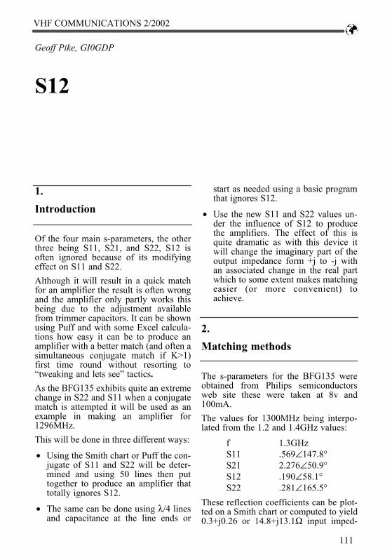
1.Introduction
Of the four main s-parameters, the otherthree being S11, S21, and S22, S12 isoften ignored because of its modifyingeffect on S11 and S22.Although it will result in a quick matchfor an amplifier the result is often wrongand the amplifier only partly works thisbeing due to the adjustment availablefrom trimmer capacitors. It can be shownusing Puff and with some Excel calcula-tions how easy it can be to produce anamplifier with a better match (and often asimultaneous conjugate match if K>1)first time round without resorting to“tweaking and lets see” tactics.As the BFG135 exhibits quite an extremechange in S22 and S11 when a conjugatematch is attempted it will be used as anexample in making an amplifier for1296MHz.This will be done in three different ways:
• Using the Smith chart or Puff the con-jugate of S11 and S22 will be deter-mined and using 50 lines then puttogether to produce an amplifier thattotally ignores S12.
• The same can be done using λ/4 linesand capacitance at the line ends or
start as needed using a basic programthat ignores S12.
• Use the new S11 and S22 values un-der the influence of S12 to producethe amplifiers. The effect of this isquite dramatic as with this device itwill change the imaginary part of theoutput impedance form +j to -j withan associated change in the real partwhich to some extent makes matchingeasier (or more convenient) toachieve.
2.Matching methods
The s-parameters for the BFG135 wereobtained from Philips semiconductorsweb site these were taken at 8v and100mA.The values for 1300MHz being interpo-lated from the 1.2 and 1.4GHz values:
f 1.3GHzS11 .569∠147.8°S21 2.276∠50.9°S12 .190∠58.1°S22 .281∠165.5°
These reflection coefficients can be plot-ted on a Smith chart or computed to yield0.3+j0.26 or 14.8+j13.1Ω input imped-
Geoff Pike, GI0GDP
S12
VHF COMMUNICATIONS 2/2002
111

Fig 1 : Matching method one.
Fig 2 : Matching method two.
VHF COMMUNICATIONS 2/2002
112

ance and 0.57+j0.08 or 28.35+j4.2Ω“output impedance” in a 50Ω system.By inspection it can be seen that thedevice has a +j imaginary input part andthe same for the output S22, also S12under these conditions is not negligibleand the result of ignoring it will bedemonstrated.
2.1 Matching method oneThe first matching method will use Puffto simply determine the length of 50Ωline that will intersect with the normal-ized admittance contour = 1. Put anotherway, the line length needed to raise thereal part of the impedance to 50Ω butwill still leave the line input impedancereactive. Puff can then be used to deter-mine the stub length to produce a reac-tance of opposite sign at this point henceleaving it purely resistive.As a personal choice this will be an o/cline and the equivalent capacitance willbe provided from a trimmer to allowsome adjustment.This is all standard stuff but Zin and Zoutconjugates will treat the 2 port device ashaving S12 being non existent.Fig 1 shows that a reasonable match doesexist however it is not what you wouldexpect from conjugate matching the inputand output, clearly the effect of S12 isapparent.This match was done using Puff to matchthe stand alone input and output imped-ances, and while you could play aboutand maybe eventually simulate a bettermatch there is a better method.
2.2 Matching method twoThe next matching scheme uses basicallythe same as above but uses a basicprogram which ignores S12 and uses1/4λ lines of the appropriate impedanceto match the devices stand alone inputand output ports.Fig 2 shows that this achieves much thesame as the previous method but uses
1/4λ lines of variable impedance to dothe matching and again discrete variablecapacitors on the lines to achieve tuning.Whilst the match is better it is still notvery good, this again being the result ofS12 affecting both S11 and in this casevery much affecting S22.
2.3 Matching method threeThe third matching scheme takes intoaccount the pronounced effect of S12 inthis example on S22. To calculate newvalues for S11 and S22 under conditionsof simultaneous conjugate match theequations in the ARRL book “UHF/Microwave experimenters manual” wereused, however they appear in other litera-ture.The calculations are tedious and it isbetter to get Excel to do it for you or towrite a program for it because it is easyto make mistakes with complex numbersin both magnitude and angle format andin polar coordinate form.Of course Puff also must use them toproduce solutions when reading from aS2P file.Fig 3 uses the new values for S11 andS22 under simultaneous conjugate matchand these are:
S11 0.643∠154.9°or 11.36+j10.4Ω
S22 0.266∠-88.3°or 43.95-j25.0Ω
A considerable improvement in returnloss for S11 at -30db and S22 at -36db isseen.Also although not often thought of inpower devices K=1.07 and thus the am-plifier is unconditionally stable.Fig 4 shows puff looking into S22 whenS11 matched. It is included to helpconfirm that when the input is matchedand terminated in 50Ω, when lookinginto its output port, S22, the impedanceseen is close to that calculated previ-ously. Puff returns S22 as 42.6-j23.1Ω
VHF COMMUNICATIONS 2/2002
113

Fig 3 : Matching method three.
Fig 4 : Looking into S22 when S11 matched.
VHF COMMUNICATIONS 2/2002
114

which compares favorable with the valueof 43.9-j25.0Ω used in Fig 3.The same result is achieved by terminat-ing the input in its new complex conju-gate i.e. 11.36-j10.4Ω using Puff to lookinto the output port, it then returns thenew S22 value as above, see Fig 5.
3.Summary
In summary it doesnt matter the way inwhich you chose to match be it either1/4λ lines of appropriate impedance, or50Ω lines of variable length or a mixtureof both.However what is important is the modi-fying effect of S12 (which is seen inpractice by the interaction of the inputand output tuning of most solid stateamplifiers) and the necessity to take its
value into account for matching net-works.
Fig 5 : Looking into output port with new input termination.
VHF COMMUNICATIONS 2/2002
115

He joined the OEVSV in1938, when he was only 14years old. He became anairborne radio operator andworked with Wernher vonBraun in Peenemünde. Hewas never to lose his enthu-siasm for modern wirelesscommunication, and hegave his heart and soul toamateur radio. His particu-lar interest was in wave-lengths from 144MHz up-wards, and he graduallyprogressed right up to
24GHz. He developedand constructed radiocomponents, which hethen subjected to com-prehensive testing.On 3rd May, 1958,Alois, OE6AP, withhis fellow amateursand long standingfriends, Emmerich( E m o ) H a r m e t ,OE6TH, Rudolf Hir-schmann, OE6RH andHeinrich Steinböck,OE6HS, embarked ona bold experiment con-cerning the first Euro-pean meteor scatter(MS) reflections. They
Eberhard L. Smolka, DB7UP
In Memorandum of Alois Pendl,OE6AP
A pioneer of VHF/UHF amateur radio
VHF COMMUNICATIONS 2/2002
116

worked 1,623m up, on the top of theFeuerkogel (Salzkammergut), in dra-matic weather conditions, with 100 Wattsat 144MHz, they used two 17 elementantennas, transmitting to SM6BTT inSweden. The experiment was a success,some time later it was followed by the
first European SSB QSO using meteorscatter (LX1DB and OE6AP).On 5th May, 1976, he was responsiblefor the first 2m EME link from Austria(JA6DR OE6AP), followed by a 70cmtransmission on 21.11.1980 (OH3TAOE6AP).
VHF COMMUNICATIONS 2/2002
117
He demonstrated tremendous commit-ment to his hobby of radio; between1959 and 1963, he was VHF manager forthe Austrian amateur radio association,ÖVSV.He was the initiator, and one of thefounders, of “VHF Reports” in 1960.Surrounded as he was by the Austrianpeaks, it came as no surprise that hefrequently took part in competitions andrange tests in the mountains e.g. on theHochwechsel, the Zugspitze, theFeuerkogel and countless others.
In recognition of his outstandingachievements in the VHF/UHF/SHFfields, The ÖVSV awarded him a com-memorative plaque in 1987.Alois Pendl, OE6AP, died on 18th March2001.Many radio hams from his own area andfrom further afield will always treasurehis memory as will the editorial teamhere at “VHF Reports”.
Eberhard L. Smolka, DB7UP
VHF COMMUNICATIONS 2/2002
118

VHF CommunicationsBack Issues
• Most back issues available from 1969 onwards, an up to datelist is maintained on the VHF Communications web site or seepage 63 of this issue. Some difficult to obtain issues can besupplied as photocopies.
• Locate interesting articles by searching the full index on theweb site, then order the magazine using the secure form on theweb. You can also order by post or fax.
• If you are new to VHF Communications magazine or havemissed some volumes or issues, choose one of the back issuesets or individual magazines to make your collectioncomplete.
• Keep your magazines in good condition with Blue Bindersthat hold 12 issues, £6.50 each + P&P
• Single issue from 1969 to 2000, £1.00 each + P&P
• Single issues from 2001 volume, £4.70 each + P&P
• Complete 2001 volume, £18.50 + P&P
• Back issue set 1972 to 1999 (51 magazines), £45.00 + P&P
• Back issue set 1972 to 2001 (59 magazines), £65.00 + P&P
K M Publications, 63 Ringwood Road, Luton, Beds, LU2 7BG, UK
Tel / Fax +44 1582 581051, web site www.vhfcomm.co.uk
VHF COMMUNICATIONS 2/2002
119

A further interesting addition to the 1- 65 MHz short-wave synthesiser fromBernd Kaa, DG4RBF, is the directmixer described below. This combineswith the second supplementary mod-ule, the AD8307 logarithmic detector,to create a spectrum analyser formeasurements in the frequency rangeof 1 - 65MHz. (The 1 - 65MHz synthe-siser has not appeared in VHF Commu-nications, only UKW Berichte. This de-sign is still of interest, if there is ademand the sysnthsiser project can betranslated and appear in a future VHFCommunications - Andy)
1.General
Since the logarithmic detector processesfrequencies down to 0Hz with the ICAD8307 (DC), the short-wave synthe-siser can be expanded into a low costspectrum analyser by simple means. Thekey concept is the direct mixing process.The HF spectrum to be measured orrepresented is mixed over the range from0 to 250kHz, with the 1 to 65MHzshort-wave synthesiser acting as the os-cillator [1]. The logarithmic detector as-sembly [2] takes charge of displaying thereading on an oscilloscope; the dynamicrange is approximately 70dB.
2.Description of circuit
The central component in this circuit(Fig. 2) is the type SBL-1 ring mixer.The deciding factor here is the frequencyresponse of the HF and LO ports, begin-ning at less than 1MHz, and the interme-diate frequency port going down to directcurrent (DC). The well known IE500mixer cant do that!To match the output from the wobbleoscillators at 10mW, the ring mixer isadjusted through a 3dB attenuator at theLO input. The level here, as shown in thespecification sheet, should be +7dBm(5mW). The HF input should be wiredup to a 10dB attenuator. Thus the maxi-mum input level for the direct mixerassembly can be 1mW (0 dBm). Highersignal strengths generate intermodulationand falsify the reading by causing addi-tional spectrum lines to be displayed.The intermediate frequency port is fol-lowed directly by a 9 pole low pass witha cut off frequency of 250kHz. Thisgives the band width required so thateven rapid measurements on short-wavetransmitters can be made. The amplifierstage with V = 10 dB guarantees match-ing to 50 to connect the logarithmicdetector assembly with AD8307.
Wolfgang Schneider, DJ8ES
Direct mixer for a 1 - 65MHzshort-wave synthesiser
VHF COMMUNICATIONS 2/2002
120
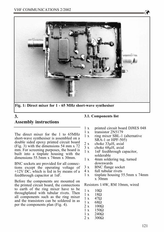
3.Assembly instructions
The direct mixer for the 1 to 65MHzshort-wave synthesiser is assembled on adouble sided epoxy printed circuit board(Fig. 3) with the dimensions 54 mm x 72mm. For screening purposes, the board isbuilt into a tinplate housing with thedimensions 55.5mm x 74mm x 30mm.BNC sockets are provided for all connec-tions except the operating voltage of+12V DC, which is fed in by means of afeedthrough capacitor at 1nF.Before the components are mounted onthe printed circuit board, the connectionsto earth of the ring mixer have to bethroughplated with tubular rivets. Thenall components such as the ring mixerand the transistors can be soldered in asper the components plan (Fig. 4).
3.1. Components list
1 x printed circuit board DJ8ES 0481 x transistor 2N51791 x ring mixer SBL-1 (alternative
SRA-1 or HPF-505)2 x choke 33µH, axial3 x choke 68µH, axial1 x 1nF feedthrough capacitor,
solderable1 x 4mm soldering tag, turned
downwards3 x BNC flange socket4 x full tubular rivets1 x tinplate housing 55.5mm x 74mm
x 30mmResistors 1/4W, RM 10mm, wired1 x 10Ω1 x 18Ω1 x 47Ω1 x 68Ω2 x 100Ω1 x 150Ω1 x 240Ω2 x 300Ω
Fig. 1: Direct mixer for 1 - 65 MHz short-wave synthesiser
VHF COMMUNICATIONS 2/2002
121

1 x 1kΩ1 x 3.3kΩCeramic capacitors, RM 2.5mm, wired2 x 4.7nF2 x 22nF1 x 27nF6 x 100nF
4.Putting into operation
Before putting it into operation for thefirst time, just check the assembly visu-ally to make sure that the components arecorrect and that there are no short cir-cuits. With an operating voltage of+12V, the circuit needs a current ofapproximately 20mA.The input power at the HF port should
Fig. 2: Direct mixer circuit.
Fig. 3: DJ8 ES 048 printed circuitboard layout.
Fig. 4: Component layout of directmixer for short-wave synthesiser.
VHF COMMUNICATIONS 2/2002
122

not exceed 1mW (0 dBm). With a higherdrive, the ring mixer goes into compres-sion and generates a great many unpleas-ant intermodulation products. These fal-sify the reading! So it makes sense toinsert a switchable attenuator in front ofthe direct mixer.
5.Working with the direct mixerassembly
If we combine the short-wave synthesiserfor 1 65MHz with DDS at the LO inputand the logarithmic detector at the inter-mediate frequency output of the directmixers, we now have a spectrum analyserfor the range 1 - 65MHz.For measurements, you need only enterthe frequency range to be observed(from/to MHz) on the short-wave synthe-siser. No intermediate frequency mis-match is taken into account!
6.Literature
[1] Bernd Kaa, DG 4 RBF: 1 - 65MHzshort-wave synthesiser with DDS, VHFReports 3/99[2] Wolfgang Schneider, DJ 8 ES:AD8307 logarithmic detector for up to500 MHz, VHF Communications 2/2000pp 119 - 124
Fig. 5: Measurement rig.
VHF COMMUNICATIONS 2/2002
123

PUFF version 2.1Microwave CAD Software
•••• Available again
•••• Complete with full English handbook
•••• Software supplied on 3.5 inch floppy disc
Price £23.50 + shipping
Shipping - UK £1.50, Surface mail £3.00, Air mail £5.00
As used in article on S12 in this issue
Visit the VHF CommunicationsWeb site www.vhfcomm.co.uk•••• Text of some past articles
•••• List of all overseas agents
•••• Secure form to subscribe and order back issues or kits
•••• Full index of VHF Communications from 1969 to the current issue,this can be searched on line or downloaded
•••• Up to date list of back issues available
•••• Links to other site including all of those from Internet Treasure Trovearticles
•••• Downloads from some article including YGO3 the Yagi designprogram
VHF COMMUNICATIONS 2/2002
124
In August 2001 The RSGB approachedme about updating the three volumeMicrowave Handbook, to produce a newsingle volume book. This was to be inassociation with The ARRL and wouldbecome The International MicrowaveHandbook.The existing three volume set handbookwas written over a period of ten years bymembers of the Microwave Committeein the UK and contains an invaluablesource of microwave theory, I am surethat many readers of VHF Communica-tions have a set in their collection. Manyof the designs had become dated, so mytask was to find up to date designs for allof the microwave bands.The first three months of the project werespent researching for designs from allaround the world. Obviously there arearticles from The RSGB and The ARRLbut I also wanted as wide a range ofmaterial as possible. This has resulted inarticles from thirty four sources, so thereis plenty of interest for everyone.Once all of the articles were found thefun really began for me. Gathering all ofthe text and diagrams, with some requir-ing translation was an enormous task,followed by big DTP job, proof readingand corrections. All of that kept me fullyoccupied for the next three months butend result is a 474 page handbookpacked full of theory, information and
designs for the microwave bands.The first eight chapters cover, operatingtechniques, system analysis and propaga-tion, antennas, transmission lines, semi-conductors and valves, construction tech-niques, common equipment and testequipment. Much of this information istaken from books one and two of theexisting hanbook with updated informa-tion on such things as MMICs, semicon-ductors and decoupling techniques.The remaining chapters cover each of theamateur bands from 23cm to 24GHz andbeyond. The band chapters have up todate designs for pre-amplifiers, transvert-ers, transceivers, power amplifiers, an-tennas and filters. These designs rangefrom true amateur construction projectsto commercially available kits.The handbook is available from TheRSGB or The ARRL, for details see thatadvertisement on the inside cover page ofthis magazine.
Andy Barter, G8ATD
Andy Barter, G8ATD
International MicrowaveHandbook
VHF COMMUNICATIONS 2/2002
125

KACHINA
Here, among other things, we can find aset of wiring diagrams for the Trans-ceiver 505DSP, which is no longermanufactured. (Obviously you can stillobtain residual stocks of this transceiverat favourable prices.) You can also lookat some application reports. Address:http://www.kachina-az.com
Synergy
The well known microwave componentmanufacturer has made a really big effortonce again and has completely revised itshomepage. So now under a specificheading we find not only data sheets butalso appropriate application notes, tech-nical documentation and technical arti-cles (from periodicals). Treasure Troveindeed!Address:http://www.synergymwave.com
NEC Archive
The website of Ray Anderson,WB6TPU, contains an NEC archive;here, among other things, you can down-load the Yagi des ign programYGO3.ZIP, this is also available from theVHF Communications web site.Address:http://www.qsl.net/wb6tpu/swindex.html
Analog Devices
A big name in the field of IC production,mainly active in analogue circuits, D/Aconverters, RF-ICs, etc. and also in dig-ital signal processors. The technicaldocumentation has been greatly ex-panded, and especially the basic tutorials(e. g. on digital signal processors). Youcan look around for hours now and findmore and more new stuff to downlowad.Address:http://www.analog.com
Gunthard Kraus, DG8GB
Internet Treasure Trove
VHF COMMUNICATIONS 2/2002
126

Software Radios
Under the precise address given below:http://www.analog.com/industry/versa-comm/apps-techInfo.htmlyou can download some interesting ap-plication reports, especially on the sub-ject of “Software Radios” .
Software and Links
Under the addresshttp://www.duncanamps.com/you can download a free program fordesigning mains rectifier circuits. In ad-dition, there are links relating, to hi-fiamplifiers and SPICE.
The Longwave Homepage
Amateur activities in the longwave areaare a really new challenge for do-it-yourselfers and for anyone who enjoysfiddling about. And it was only a matterof time until like minded people met upand got organised on the Internet as well.This homepage is the first address any-one interested in longwave receptionshould visit, as here you can find thetechnical equipment for getting started,both theoretically and practically. Andnaturally there are lots of links to similarsites or interesting documents.Address:http://www.lwca.org
Notice
Because of the fast-moving nature of theInternet and because Internet addressesor sub-directories in homepages canchange at any time in ways which cannot be monitored, it is impossible toreflect the current situation at all times.We therefore apologise for any incon-venience if Internet addresses listed inany “Internet Treasure Trove” articles areno longer available, or are altered at shortnotice by the operators in question.However, the editors and/or the authorwill be happy to assist in finding the newaddresses for the sites in question, or inobtaining the documents required.We would also like to take this opportu-nity to point out that the author and thepublishers accept no responsibility forthe accuracy of any information listedhere!
VHF COMMUNICATIONS 2/2002
127
AUSTRALIA - W.I.A. South Australia Division, GPO Box 1234,Adelaide, SA 5001, Australia. Tel/Fax: 8 8522 4859BELGIUM - UKW-BERICHTE, POB 80, D-91081 BAIERSDORF,Germany. Tel: 09133-77980. Fax: 09133-779833 .Postgiro Nbg. 30445-858.DENMARK - KM PUBLICATIONS , 63 Ringwood Road,LUTON, LU2 7BG, UK. Tel: +44 1582 581051.
Fax: +44 1582 581051. Email: [email protected] - Christiane Michel F5SM, Les Pillets, 89240 PARLY,FranceFax: (33) 03 86 44 08 82 Tel: (33) 03 86 44 06 91FINLAND - KM PUBLICATIONS , 63 Ringwood Road, LUTON,LU2 7BG, UK. Tel: +44 1582 581051.Fax: +44 1582 581051. Email: [email protected] - UKW-BERICHTE, POB 80, D-91081BAIERSDORF, Germany. Tel: 09133 7798-0. Fax: 09133 779833.GREECE - KM PUBLICATIONS , 63 Ringwood Road, LUTON,LU2 7BG, UK. Tel: +44 1582 581051.Fax: +44 1582 581051. Email: [email protected] - KM PUBLICATIONS , 63 Ringwood Road, LUTON,LU2 7BG, UK. Tel: +44 1582 581051.Fax: +44 1582 581051. Email: [email protected] - R.F. Elettronica di Rota Franco, Via Dante 5 - 20030Senago, MI, ItalyFax 0299 48 92 76 Tel. 02 99 48 75 15NEW ZEALAND - KM PUBLICATIONS , 63 Ringwood Road,LUTON, LU2 7BG, UK. Tel: +44 1582 581051.Fax: +44 1582 581051. Email: [email protected] - WAVELINE AB, Box 60224, S-216 09 MALMÖ,Sweden. Tel: +46 40 16 42 66. Fax: +46 40 15 05 07.GSM: 0705 16 42 66e-mail: [email protected] http://www.algonet.se/~wavelineSOUTH AFRICA - KM PUBLICATIONS , 63 Ringwood Road,LUTON, LU2 7BG, UK. Tel: +44 1582 581051.Fax: +44 1582 581051. Email: [email protected] & PORTUGAL - JULIO A. PRIETO ALONSO EA4CJ,Donoso Cortes 58 5° -B, MADRID 15, Spain. Tel: 543 83 84SWEDEN - WAVELINE AB, Box 60224, S-216 09 MALMÖ,Sweden. Tel: 040 16 42 66. Fax: 040 15 05 07. GSM: 0705 16 4266 e-mail: [email protected] http://www.algonet.se/~wavelineSWITZERLAND - KM PUBLICATIONS , 63 Ringwood Road,LUTON, LU2 7BG, UK. Tel: +44 1582 581051.Fax: +44 1582 581051. Email: [email protected] KINGDOM - KM PUBLICATIONS , 63 Ringwood Road,LUTON, LU2 7BG, UK. Tel: +44 1582 581051.Fax: +44 1582 581051. Email: [email protected]. - GENE HARLAN, ATVQ Magazine, 5931 Alma Drive,Rockford, IL 61108, USA. Tel: Toll free USA only: 800 557 9469;Elsewhere: +1 815 398 2683; Fax: +1 815 398 2688Email: [email protected] - KM PUBLICATIONS, address as for the U.K.
WWW: http://www.vhfcomm.co.uk
KM PUBLICATIONS,63 Ringwood Road, Luton,LU2 7BG, United KingdomTel: +44 1582 581051Fax: +44 1582 581051
Email:[email protected]
Andy Barter G8ATDThe international edition of theGerman publication UKW-Berichteis a quarterly amateur radiomagazine, especially catering forthe VHF/UHF/SHF technology.It is owned and published in theUnited Kingdom in Spring,Summer, Autumn and Winter byKM PUBLICATIONS.The 2001 subscription price is£20.00, or national equivalent.Individual copies are available at£5.00, or national equivalent each.Subscriptions should be addressedto the national representative shownin the next column. Orders forindividual copies of the magazine ,back issues, kits, binders, or anyother enquiries should be addresseddirectly to the publishers.NOTICE: No guarantee is giventhat the circuits, plans and PCBdesigns published are free ofintellectual property rights.Commercial supply of these designswithout the agreement of theAuthor and Publisher is notallowed. Users should also takenotice of all relevant laws andregulations when designing,constructing and operating radiodevices.
All rights reserved. Reprints,translations, or extracts only withthe written approval of thepublishersTranslated by: Inter-Ling Services,62 Caldecott Street, Rugby,CV21 3TH, UKPrinted in the United Kingdom by:Cramphorn Colour Printers Ltd.,15a Boughton Road IndustrialEstate, Rugby CV21 1BQ, UK.
Publishers
Editor
VHFCOMMUNICATIONS
© KMPUBLICATIONS
ISSN 0177-7505
A Publication for the Radio Amateur Worldwide
Especially Covering VHF, UHF and Microwaves
Volume No.34 Summer Edition 2002-Q2
VHFCOMMUNICATIONS

The microwave bands arean excellent area for radioamateurs who want to ex-periment and constructtheir own equipment. TheRSGB in partnership withthe ARRL has producedthis invaluable source ofreference information forthose interested in thisarea, along with excellentdesigns from around theworld to fire the imagina-tion. Material has beendrawn from many sourcesincluding the RSGB jour-nal RadCom and theARRL publications QST& QEX. Alongside thismaterial a truly interna-tional range of sourceshave been used includingitems from Germany,Denmark, New Zealand,Slovenian and many more.The earlier chapters of thebook provide invaluablereference material re-quired by all interested in
this exciting area of experimentation. Techniques and devices are covered indepth, leading the reader to understand better the wide range of equipment andtechniques now available to the microwave experimenter. This book contains awide selection of designs using the latest technology that can reasonably beused by radio amateurs and ranges from ones that can be reproduced by mostradio amateurs to those that require a high degree of skill to make.With the explosion in consumer electronics using microwave frequencies theopportunity to experiment has never been greater and this book is simply thebest guide to the area of microwave radio.
Available in the UK for £24.99 from www.rsgb.org/shopAvailable in the USA for $39.95 from www.arrl.org
The New International Microwave Handbook

COMPLETE KITS, PCB's & ICs ARE AVAILABLEFOR RECENT PROJECTS
If the kit or PCB is not in this list please contact K. M. PublicationsKIT DESCRIPTION ISSUE No. PRICEDG4RBF-007 4 GHz Frequency divider 1/00 06117 £ 42.00DG4RBF-008 100 MHz Frequency Divider 1/00 06139 £ 18.50DG4RBF-009 Frequency Counter - including TXCO 1/00 06141 £ 105.00DG4RBF-010 FC4000 Micro Controller (Uniboard C501) +EPROM1/00 06143 £ 85.00DG4RBF FC4000 Complete Kit 1/00 06145 £ 240.00DJ8ES-042 2 Mtr Transceiver Function Key Assembly 1/00 06038 £ 12.00DJ8ES-043 2 Mtr Transceiver DDS 1/00 06561 £ 65.00DJ8ES-044 2 Mtr Transceiver Exciter 1/00 06563 £ 95.00DJ8ES-045 2 Mtr Transceiver Transmit / Receive Mixer 1/00 06565 £ 90.00DJ8ES 2 Mtr Micro Controller (Uniboard C501) +EPROM 1/00 06566 £ 85.00DJ8ES-047 Log Amplifier up to 500MHz with AD8307 2/00 06571 £ 42.00DG6RBP-002 Pre Divider (:10) up to 5GHz 1/02 £ 115.00DB6NT-Rotor Simple Speed Control for Rotators 2/02 06533 £ 35.00PCB DESCRIPTION ISSUE No. PRICEDG4RBF-007 4 GHz Frequency divider 1/00 06116 £ 7.00DG4RBF-008 100 MHz Frequency Divider 1/00 06138 £ 8.50DG4RBF-009 Frequency Counter 1/00 06140 £ 10.50DG4RBF-010 FC4000 Micro Controller (Uniboard C501) 1/00 06142 £ 23.00DG4RBF FC4000 Complete Kit of PCBs 1/00 06144 £ 48.00DJ8ES-042 2 Mtr Transceiver Function Key Assembly 1/00 06037 £ 5.00DJ8ES-043 2 Mtr Transceiver DDS 1/00 06560 £ 8.00DJ8ES-044 2 Mtr Transceiver Exciter 1/00 06562 £ 10.50DJ8ES-045 2 Mtr Transceiver Transmit / Receive Mixer 1/00 06564 £ 10.00DJ8ES Micro Controller (Uniboard C501) + 2 Mtr EPROM 1/00 06131 £ 50.00S53MV Set of PCBs for Matjaz Vidmar Spectrum Analyser 4/98-4/99 S53MV £ 55.00DJ8ES-047 Log Amplifier up to 500MHz using AD8307 2/00 06569 £ 6.50DG6RBP-002 Pre Divider (:10) up to 5GHz 1/02 £ 18.00DB6NT-Rotor Simple Speed Control for Rotators 2/02 06532 £ 5.50ICs DESCRIPTION ISSUE No. PRICEDJ8ES AT90S2313 For Digital Speech Store 2/01 10354 £ 17.25DJ8ES/DL5HAT AT89C52 For GPS Control Of 10 MHz Standard 1/01 10353 £ 21.50
Minimum shipping charge £5.00K. M. Publications, 63 Ringwood Road, Luton, Beds, LU2 7BG, U.K.
Tel / Fax +44 1582 581051 email [email protected] Site http://www.vhfcomm.co.uk