Embed Size (px)
Citation preview

Design With Confidence
Advanced Design System
Agilent EEsof EDA

2
“With all of the pressures on our customers to get their new products to market quickly, Agilent is uniquely positioned to help reduce the overall design cycle by supplying both EDA toolsand Test and Measurement equipment. As one company, Agilent EEsof EDA and Agilent Test Equipment will allow a more cohesive solution as design teams move from virtual simulations tobuilding and measuring actual parts. The end result for our customers will be smoother, more complete design flows and, ultimately, shorter designcycles, allowing them to innovate more quickly.
Since our acquisition of EEsof, we haveexpanded our investment in EDA and have developed worldwide customeragreements and partnerships with many of the industry’s leading companies. Our focus on high-frequency EDA continues to increase.”
Ned BarnholtPresident and CEOAgilent Technologies
Agilent Technologies dates back to1939, when Bill Hewlett and DavePackard started Hewlett-Packardand began a legacy that has shapedSilicon Valley and the technologyindustry. Its Electronic DesignAutomation (EDA) business grewfrom an internal need to improvethe design process for its RF andmicrowave instrumentation.
For more than 20 years, Agilent has led the development of newhigh-frequency EDA technologiessuch as Harmonic Balance andCircuit Envelope simulators,RF/Analog/DSP co-simulation, andbehavioral models. It is technologythat has proven its robustness and lasting value over time.
Today, just as Agilent engineers continue to use these EDA toolswhen inventing new products, you can trust that Agilent EEsofEDA supplies the breadth of technology to give you confidence in all your high-frequency designs.
“ Agilent EEsof EDA is not just a pure software company. It is part of a larger company that has RF designers, fabrication facilities, and
a modeling group. Agilent understands what we are trying to do because they do it themselves. This was a big factor in choosing
ADS as our exclusive RF design tool.” – Shihab Al-Kuran, Director of Design Technology Engineering, ANADIGICS, Inc.
World-Class Products for the Entire Development Process
Agilent EEsof EDA offers three mainplatforms, each with a wide range of affordable configurations.
• Advanced Design System (ADS), a powerful EDA software platform, offers industry leading simulation technologies to RF and Microwave designers.
• Device Modeling Systems, based upon IC-CAP parameter extraction and device modeling software, provide a complete toolset for developing accurate device models.
• ValiFire design verification systems bridge the gap between simulation and test, with preconfigured and preracked systems that use ADS for virtual design and test instrumentation for physical design verification.
Get the Competitive Advantage...
A growing number of leading companies offer Design Kits that support ADS.
IBM is a registered trademark of International Business Machines Corporation.
www.agilent.com/find/eesof-foundries
3
“ TSMC’s support for Agilent’s leading RF simulation environment reflects the strong demand by designers for state-of-the-art
analysis as they prepare these products for market.” – Genda Hu, Vice President of Corporate Marketing, TSMC.
Leading through Partnerships
Industry partnerships enable ADS to lead the way to efficient, streamlined design and verification.The number of partners is steadilygrowing, so you can be sure of anever-expanding sphere of innovationwith ADS.
• Foundry Partners – For MMIC orRFIC design, Agilent has formed strategic partnerships with many leading semiconductor foundries to provide RFIC and MMIC DesignKits that enable you to access powerful simulation technologies available in ADS.
• Application Partners – Over a dozen application partners have taken advantage of the ADSopen architecture to add value by expanding on its capabilities to create DesignGuides that set up and streamline real-world circuit designs.
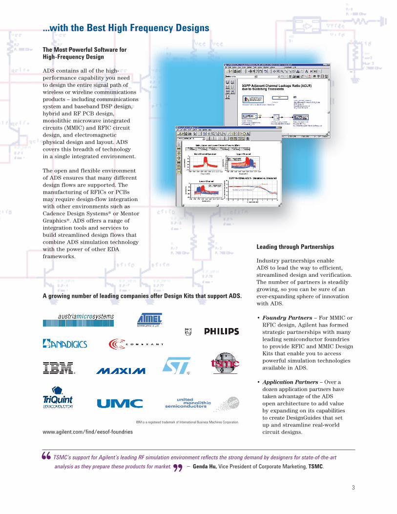
The Most Powerful Software forHigh-Frequency Design
ADS contains all of the high-performance capability you need to design the entire signal path ofwireless or wireline communicationsproducts – including communicationssystem and baseband DSP design,hybrid and RF PCB design, monolithic microwave integrated circuits (MMIC) and RFIC circuitdesign, and electromagnetic physical design and layout. ADS covers this breadth of technology in a single integrated environment.
The open and flexible environmentof ADS ensures that many differentdesign flows are supported. Themanufacturing of RFICs or PCBsmay require design-flow integrationwith other environments such asCadence Design Systems® or MentorGraphics®. ADS offers a range ofintegration tools and services tobuild streamlined design flows thatcombine ADS simulation technologywith the power of other EDA frameworks.
...with the Best High Frequency Designs

“ Your DesignGuides have saved me lots of time in my daily design work.” – Francis Yu, Design Engineer, Nokia Mobile Phones, Inc.
4
The Simulation Technology Layer
Designing circuits for different functional blocks often requires different simulation technologies.ADS offers the most complete spectrum of simulation technologies.When combined, they enable you to fully characterize and optimizedesigns under multiple conditions. The result is a product that can exceed performance requirementsand be manufactured at high volumes.
Reduce Design Time...
The Application Layer
Ease of use is important for EDAtools, and ADS is continually beingimproved in this area. “Ease of design”is even more critical as it can have adirect impact on completing yourdesigns as fast as possible. This iswhy the application layer in ADS is so important. DesignGuides,Design Libraries, DesignSeminars,and application training are allaimed at bridging the gap betweensimulation technology and yourapplications.
The Models Layer
Accurate models are a prerequisite for any successful design flow. Withoutgood models, designers can’t makeprogress or have confidence in their simulation results. Agilentoffers numerous models within ADS:
• RF system models that enable mixed-signal verification with over1500 analog, RF, and DSP models
• Design Libraries with models for the latest communication standard modulation formats
• ADS component libraries with over 100,000 parts
• MMIC/RFIC Design Kits availablefrom leading foundries
In addition, there are severaloptions available to let you developcustomized models to meet yourspecific device and product requirements:
• Modeling systems for developing accurate device model extractions
• Model Composer, which uses a unique EM modeling method for customizing existing passive planar elements
• Consulting on modeling processesand model-extraction services
• Model Development Kit for generating user-defined models
ADS is an environment that tightly integrates several powerful simulation technologies. It allows you to develop or import RF, analog, and DSP intellectual property, and model key interactions.
DesignGuides Design Libraries
Use powerful ADS simulation technologies Verify your designs against communicationin an application-focused way. standards. Design Libraries include preconfiguredDesignGuides include simulation setups, measurement setups and built-in signal sources data displays, and documentation. based on the latest standards.
Available DesignGuides include: Available Design Libraries include:
RF System DesignGuide CDMA Design LibraryPower Amplifier DesignGuide GSM Design LibraryMixer DesignGuide 5-GHz WLAN Design LibraryOscillator DesignGuide DTV Design LibraryPassive Circuit DesignGuide 3GPP Design LibraryFilter DesignGuide cdma2000-Compliant Design Library PLL DesignGuide EDGE Design LibraryLinearization DesignGuide 1xEV-DO Design Library cdma2000 DesignGuideBluetooth® DesignGuideWLAN DesignGuide DesignGuide Developer Studio
www.agilent.com/find/eesof-desguides www.agilent.com/find/eesof-deslibs

5
Advanced Architecture
The architecture behind ADS represents flexibility for designers.Unlike that of any other EDA vendor, our software was designedfrom the start for full functionalityon both the PC and on UNIX workstations. This multi-platformarchitecture allows you to design
...and Get to Market Faster
EDA and Instrumentation Integration
The ability to closely integrate EDAsoftware with test instrumentationhelps you reduce design time byallowing the evaluation of hardwareprototype subsystems. For example,real-world signals that include propagation effects can be modeledin ADS, input to an Agilent signalgenerator, and connected to a deviceunder test for prototype testing. This is a powerful tool to remove the associated uncertainties whencorrelating measured results withmodeled results. Designs, data, andsignals can seamlessly flow betweenthe virtual and physical worlds,ensuring that you get the best possible verification of your development investment prior tofabrication.
“ New wireless and wireline products are the result of creative design and innovative manufacturing. ADS supports these efforts at
both the circuit and system levels with accurate simulation and the capacity to handle large, complex systems.”– Gary Breed, Former Publisher of Applied Microwave & Wireless Magazine
In addition to instrument integration,links to Agilent VEE allow instrumentcontrol and complete sharing andmanipulation of data as well asautomation of the test setup, enablingyou to create customized design-verification solutions.
on the road but still have completefile compatibility with the designteam in the office. And because ADS runs on UNIX, it can be integrated with other EDA vendors to ensure your designs get to market fast.
The ADS platform also enhancesdesign efficiency by facilitating co-design throughout the completedesign cycle. Designers responsiblefor different stages of the work can use the same design platform,database, and testing environment.

6
The Support You Need When and Where You Need It
Agilent EEsof EDA’s worldwideproduct support infrastructurestands ready to help you use ADS toconquer your design and developmentchallenges. This product supportincludes substantial softwareupgrades, manual updates, andinformation and assistance via telephone, fax, e-mail, and the Web.
In a world where not only yourproduct goes international but inmany cases your design team is alsointernational, you need to ensurethat support will be there when andwhere you need it. Agilent EEsofEDA’s international support is provided by four main centers thatspeak the local language and workin the same time zone. Your designteam members around the globe do not want to have to work in themiddle of the night just to obtainreal-time technical support from a North American support center.Wherever you need assistance,Agilent EEsof EDA is already there,ready to help.
www.agilent.com/find/eesof-support
Our worldwide supportengineers understandyour design problemsand are ready to help.
Specialized Consulting Services
You can make further use of Agilent EEsof EDA’s broad expertisethrough its array of custom solutionservices designed to improve processefficiency and tool productivity inall aspects of design work:
• Design process consulting assesses design process strengths and weaknesses and recommends opportunities for improvement.
• Interfacing and translation services help to integrate Agilent EEsof EDA design tools to yourdesign flow.
• Application customization tailors Agilent EEsof EDA tools to your specific application or use-model.
• Model customization provides modeling expertise for your special structures, from passive elements to whole systems.
Get the Most...
An independent EDA industry survey ranked Agilent EEsof EDA #1 in customer satisfaction.

“ I really appreciated the Agilent EEsof training class. The presentation of ADS capabilities, such as how to simulate an entire
communication link and integrate RF with Ptolemy, was excellent.” – Peter Denney, RF/Antenna Engineer, Harris Corporation
7
High-Quality Training, in Your Regionor at Your Site
Agilent EEsof EDA’s worldwidetraining centers provide high-quality education to your team members. You can choose from product-oriented classes to get up to speed on how to operate thetools, or design-oriented classes to see how the tools are used foractual design tasks.
Agilent EEsof EDA has been training engineers for many yearsand has perfected the process. A combination of lectures and labs provides hands-on practicalexperience in an accelerated learning environment. The lecturesprovide detailed concepts and theory while the labs provide timein front of the tools working on real-world designs.
These classes are taught by AgilentEEsof EDA technical support engineers as well as industry andacademic specialists. Training can be conducted on site, in a classroom, or via the web. You canalso have the training customized to fit your next project to furtherimprove the learning curve andmove your team quickly from thetool-learning phase into the development stage.
www.agilent.com/find/eesof-class
Affordable ADS Solutions
Agilent EEsof EDA has a wide variety of flexible plans to workwithin your budget. ADS productsspan a full range of offerings from economical foundation toolsetsto advanced premium suites. Time-based licenses and packageleases are available to give you the tools you need for the length of time you need them.Industry-standard perpetual licenses also are available.
...from Your Investment
Agilent EEsof EDA on the World Wide Web
Product details, application information, and technical supportare available for Advanced DesignSystem and all other Agilent EEsofEDA products 24 hours a day, everyday of the year, on the Agilent EEsof EDA world wide web site:
http://www.agilent.com/eesof-eda
The web site is extensive anddynamic. It is the place to find the latest products, application examples,events, and educational webcastannouncements. It also containsproduct documentation, trainingclass schedules, on-line registration, and in-depth technical supportinformation, including an easilyaccessible support database of technical and product informationand downloadable files.

For more information about Agilent EEsof EDA,visit:
www.agilent.com/eesof-eda
For more assistance with your test and measurement needs, visit:
www.agilent.com/find/assist
Phone or Fax: Canada:United States: (tel) 1-877-894-4414(tel) 1-800-452-4844 (fax) (905) 282-6495
Europe: Japan:(tel) (31 20) 547-2323 (tel) (81) 426-56-7832(fax) (31 20) 547-2390 (fax) (81) 426-56-7840
Latin America: Australia:(tel) (305) 269-7500 (tel) 1-800-629-485(fax) (305) 269-7599 (fax) (613) 9210-5947
New Zealand: Asia Pacific:(tel) 0-800-738-378 (tel) (852) 3197-7777(fax) 64-4-495-8950 (fax) (852) 2506-9284
Product specifications and descriptions in thisdocument subject to change without notice.
© Agilent Technologies, Inc. 2001 Printed in USA, October 11, 20015988-3326EN
Cadence is a registered trademark of Cadence Design Systems, Inc.
Mentor Graphics is a registered trademark of Mentor Graphics Corporation in the U.S. and other countries.
Bluetooth and the Bluetooth logos are trademarks owned by Bluetooth SIG, Inc. USA and licensed to Agilent Technologies.