Embed Size (px)
Citation preview

ASM InternationalAnalyst and Investor Technology Seminar Semicon West July 15, 2015
ADVANCED WAFER PROCESSING WITH NEW MATERIALS

| 2
SAFE HARBOR STATEMENTS
Safe Harbor Statement under the U.S. Private Securities Litigation Reform Act of 1995: All
matters discussed in this business and strategy update, except for any historical data, are
forward-looking statements. Forward-looking statements involve risks and uncertainties that
could cause actual results to differ materially from those in the forward-looking statements.
These include, but are not limited to, economic conditions and trends in the semiconductor
industry generally and the timing of the industry cycles specifically, currency fluctuations,
corporate transactions, financing and liquidity matters, the success of restructurings, the timing
of significant orders, market acceptance of new products, competitive factors, litigation involving
intellectual property, shareholder and other issues, commercial and economic disruption due to
natural disasters, terrorist activity, armed conflict or political instability, epidemics and other
risks indicated in the Company's filings from time to time with the U.S. Securities and Exchange
Commission, including, but not limited to, the Company’s reports on Form 20-F and Form 6-K.
The company assumes no obligation to update or revise any forward-looking statements to
reflect future developments or circumstances.

| 3
OUTLINE
› New Materials and 3D: Moore’s law enablers› ASM and New Materials
• ALD as enabler of new materials
• ASM New Materials development strategy
• ALD supply chain components
› ASM Products and selected applications› Summary and Conclusions

| 4
OUTLINE
› New Materials and 3D: Moore’s law enablers› ASM and New Materials
• ALD as enabler of new materials
• ASM New Materials development strategy
• ALD supply chain components
› ASM Products and selected applications› Summary and Conclusions

| 5
SCALING IS INCREASINGLY ENABLED BY NEW MATERIALS AND 3D TECHNOLOGIES
Scaling enabled by Litho
Scaling enabled by Materials
Scaling enabled by 3D
1995 2000 2005 2010 20151990 20252020
Strained Si
High-k
3D Memory
IEDM 2002
IEDM 2003
IEDM 2007
3D TSV
Confidential and Proprietary Information
PatterningSpacers
Low-k
FinFET
GAA
High-mobility Materials

| 6
SCALING BY MATERIALS AND 3D
• Density scaling (continuing Moore’s law) driving towards higher mobility materials and alternate device architectures
• Future systems will integrate much wider variety of materials and device structures
ASM Proprietary and Confidential Information
14-22nm 1xnm
≤7nm≤5nm

| 7
NEW MATERIALS AND PROCESSES: MOORE’S LAW ENABLERS
Higher Capacitance, Lower Leakage
High-k / Metal Gate
DRAM, RF, decoupling capacitors
Smaller Feature Sizes
Sub-Rayleigh limit patterning using SDDP
Less Cross Talk, Faster Interconnect
(Porous) Low-k Materials
Improved Metals
(C) Intel
Higher Mobility, Lower Resistance
Strain and new Channel MaterialsNew metal contacts
STISi
High-k /metal gate
S/D stressor /contact
STI
Spacer

| 8
INCREASING INTRODUCTION RATE OF NEW MATERIALS
1960 1970 1980 1990 2000 2010
SOI
CuSiOF
SiGe
NiSiSi(O)N
WTi/TiN
(B)PSG
Si,epiSiO,NAl-Cu
SOPSiOC
AlOHf(Si)O
Ta/TaN
TaO
ZrOLaOSiC
CuSiOFCoSi
Si(O)N
WTi/TiN
(B)PSG
Si,epiSiO,NAl-Cu
SOPSiOC
Ta/TaN
TaO
TiSiSi(O)N
WSi, PtSiTi/TiN
(B)PSG
Si,epiSiO,NAl-Cu
Si(O)N
WSi, MoSiTiW
(B)PSG
Si,epiSiO,NAl-Cu
(B)PSG
Si,epiSiO, SiNAl-Cu
SiSiO, SiNAl-Cu
Starting Mat’lFEOLBEOL
SOI
CuSiOF
SiGe
NiSiSi(O)N
WTi/TiN
(B)PSG
Si,epiSiO,NAl-Cu
SOPSiOC
AlOHf(Si)O
Ta/TaN
TaO
ZrOLaOSiC
SiPSiCP
CoWPCo
2015
Porous SiOC
TiC

| 9
OUTLINE
› New Materials and 3D: Moore’s law enablers› ASM and New Materials
• ALD as enabler of new materials
• ASM New Materials development strategy
• ALD supply chain components
› ASM Products and selected applications› Summary and Conclusions

| 10
ASM AND NEW MATERIALS
› ASM technology focuses on enabling new materials and new device
integration roadmaps 3D transistor formation (FinFET & beyond FinFET)
DRAM, Flash and emerging memory
More than Moore / IoT applications (MEMS, Sensors, Power)
› ALD and PEALD as enablers of new materials ALD high-k metal gates
PEALD low temp spacers for multi-patterning
Other emerging applications

| 11
ALD AS ENABLER OF NEW MATERIALS -KEY STRENGTHS OF ALD
Step Coverage
SEM’s Courtesy of Philips Research Labs
TiN
Uniformity
Max
Min
<1% 3<0.7% M-m
29 nm SiO2
Interface Control
Atomically engineered interfaces to optimize leakage current, reliability and work-functions
Composition Control
Excellent composition control for ternary alloys; all ALD solution demonstrated for GST
Ritala, E/Pcos 2012;

| 12
Process Integration
ASM NEW MATERIALS DEVELOPMENT STRATEGY
N+≥3 New Materials Screening
N+2,3
Product DevelopmentN+1,2
ASM MicroChemistry, Finland
• Basic materials R&D• Chemical synthesis• Pre-cursor screening
ASMB @IMEC, Belgium
• Process development• Integration• Device characterization
Product Line Site• Engineering• Product development• Product marketing
Cus
tom
er jo
int d
evel
opm
ent

| 13
CRITICAL ALD SUPPLY CHAIN COMPONENTS
Fundamental Capability
Process Performance Productivity Integrated
ProcessFinal Product
Capability
Pre-cursors
Pre-cursor Delivery, Valves
and Vessels
Reactors
Fab facilities,pumps & abatement
High productivity tools

| 14
OUTLINE
› New Materials and 3D: Moore’s law enablers› ASM and New Materials
• ALD as enabler of new materials
• ASM New Materials development strategy
• ALD supply chain components
› ASM Products and selected applications› Summary and Conclusions

| 15
ASM PRODUCTS ALD
15
EmerALD® XP
Pulsar® XP
›Pulsar® XP ALD for high-k
Cross-flow reactor
Solid source delivery system
›EmerALD® XP ALD for metal gates
Showerhead reactor

| 16
FINFET CHALLENGES:ALD ENABLES FURTHER SCALING IN 3D
• Materials properties and channel length must be uniform over fin height• Conformal coverage required• Aspect ratios increase going from 22nm to 14nm• ALD technology has become critical for HK and MG layers
Source: Intel

| 17
EXTENDIBILITY OF HAFNIUM BASED OXIDES
chipworks chipworks
45nm HK first RPMGPlanar FET
32 nm HK last RPMGPlanar FET
28nm HK first RPMGPlanar FET
22nm HK last RPMGFinFET
chipworks chipworks
chipworks
14nm HK last RPMGFinFET

| 18
ASM PRODUCTSPEALD AND PECVD
›XP8-DCM High productivity single wafer tool for both PEALD and PECVD
applications
Accommodates up to 8 chambers by DCM
PEALD and PECVD can be integrated on the same platform
DCM (Dual Chamber Module)

| 19
PEALD SiO2 Spacer
Anisotropic Etch
Pitch: P
Pitch: 1/2 P
80nmPitch: 1/2 P
2nd ALD Spacer
2nd Anisotropic Etch
Pitch: 1/4 P
Hard Mask Etch
20nm
ALD ENABLING SUB-RAYLEIGH LIMIT LITHOGRAPHY WITH SPACER DEFINED DOUBLE/QUADRUPLE PATTERNING
PEALD SiO2 on resist
Spacer Defined Double Patterning with PEALD in production since 3x nm DRAM and Flash
Spacer Defined Quadruple Pattering in production for 1x nm Flash
Key enablers brought by PEALD• Uniformity: CD control• Low temperatures (<100C)• Good step coverage• Dense film• In-situ trimming capability• Extendible to other materials with high etch
selective
40nm
In-situ trimming

| 20
LINERS AND SPACERS FOR BEYOND 15nm FinFET’S
PEALD SiO2 and Si3N4 permanent spacers Low temperature (300 ~ 550 C)
High conformality
High quality (low WER, low leakage current)
40nm pitch
PEALD SiO PEALD SiN

| 21
PEALD DOPED OXIDES; SOLUTION FOR FINFETDOPING
BENEFITS:› Ability to dope selective regions in vertical direction› Low damage / substrate consumption vs. Ion Implant
Process Flow 1“Bottom Fin Doping”
Subfin doping for punch-through stopper
Process Flow 2“Top Fin Doping”
Channel/SD extension
Doped region
Integration Concept
Doped Oxide AnnealSi substrate Oxide removal(Optional)

| 22
ASM PRODUCTS ADVANCED EPITAXY
22
Intrepid® XP
› Advanced transistors enabled with Intrepid® XP
Relaxed & strained epitaxy for Si, SiGe & Ge based FinFETsthrough 7nm
Channel (SRBs), S/D stressor, contact & passivation cap layer
› Integrated, low thermal budget pre-clean module High quality surface with low interface contamination
› High productivity & lowest CoO
XP Platform with up to 4 process modules• Flexible configuration with pre-clean (3+1& 2+2)
Differentiated film growth processes enabling devices with high drive currents & best-in-class productivity
High throughput with pulsed Epi processes & high doping levels
| 23
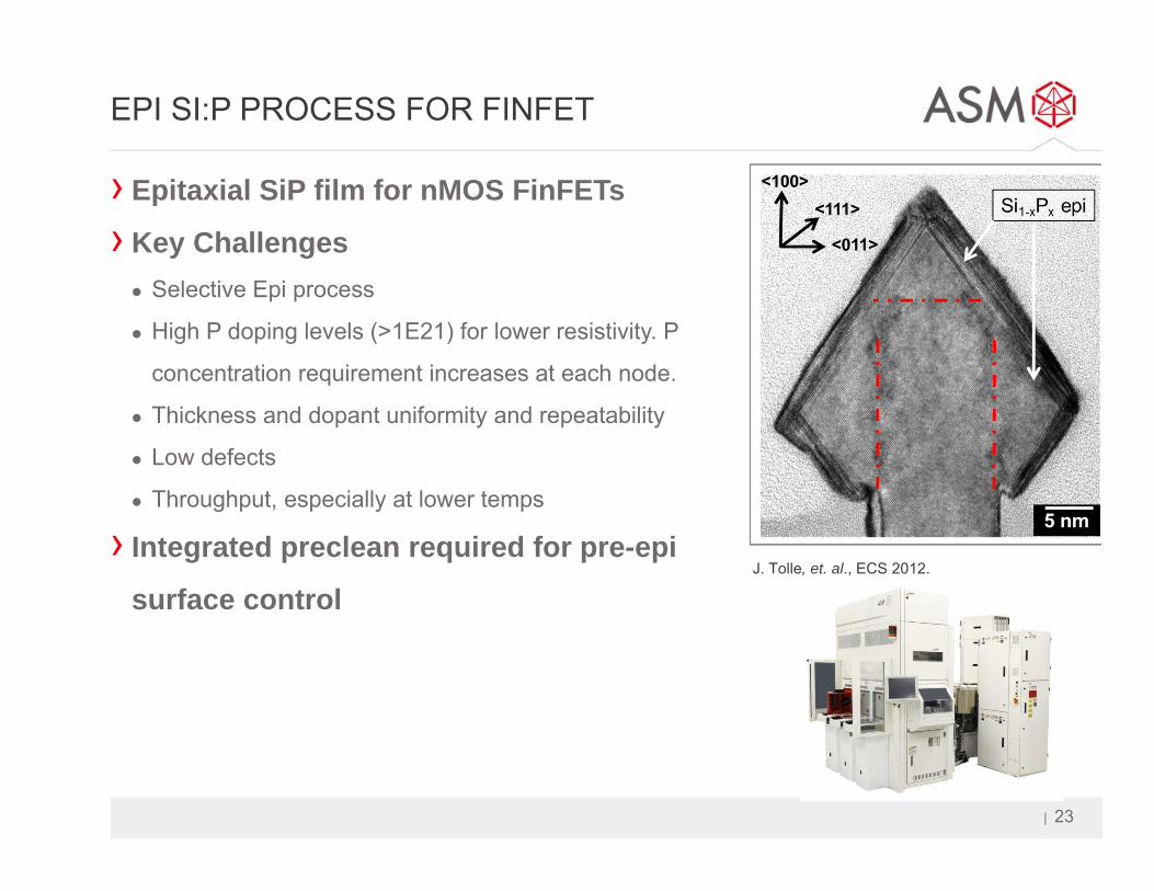
EPI SI:P PROCESS FOR FINFET
› Epitaxial SiP film for nMOS FinFETs
› Key Challenges Selective Epi process
High P doping levels (>1E21) for lower resistivity. P
concentration requirement increases at each node.
Thickness and dopant uniformity and repeatability
Low defects
Throughput, especially at lower temps
› Integrated preclean required for pre-epi
surface controlJ. Tolle, et. al., ECS 2012.

| 24
EPI LAYERS FOR POWER DEVICESMULTI-LAYER EPI TECHNOLOGY
› Power devices require multiple & thick Epitaxial films to withstand high breakdown voltages (600V ~ 800V)
› Breakdown voltage of the device dictates number of Epi layers needed
› Doping level and uniformity of the Epi layers is critical and an ASM advantage
› In HVM at several power device manufacturers enabled by:
24
N+ Drain1st layer Epi
PR mask
B implant B implant
N+ Drain
1st layer Epi
2nd layer Epi
N+ Drain
1st layer Epi
2nd layer Epi3rd layer Epi
B implant B implant
PR mask
4th layer EpiMultiple epi steps
ASM Product: Epsilon® 3200

| 25
ASM PRODUCTS FURNACE CVD /DIFFUSION /BATCH ALD
› A412 PLUS Dual boat/dual reactor system Clustering of different applications between
reactors possible – only vertical furnace in the market with this capability
Up to 150 product wafer load size New stocker design with integrated N2-FOUP
purge and 36 FOUP positions
› Applications:
Full range of applications for Logic, Memory, Power and MEMS
LPCVD Silicon, SiN, TEOS, HTO Diffusion, Anneal, Cure, Reactive Cure Pulsed CVD and Batch ALD (AlO, AlN, TiN, SiN,
SiO etc)
• No defects• No pattern collapse• No line wiggling

| 26
A400/A412 FURNACE - INNOVATION
Example 2: ALD assisted Directed Self Assembly (DSA)› DSA is a promising patterning
technique for 7nm and beyond› Combining DSA with Selective ALD
boosts the etch resistance of DSA polymers and reduces Line Etch Roughness by >40%
› Parallel lines of selective Al2O3 deposited on A412 furnace, 14 nm half pitch (SPIE conference, 2015):
Example 1: Voidless silicon gapfill. › Filling of trenches of rectangular shape
imposes challenge for voidless gapfill in >14nm. › Standard silicon gap fill:
› ASM solution. Voidless silicon gap fill:
Void

| 27
0.0
5.0
10.0
15.0
20.0
25.0
30.0
35.0
40.0
2013 2014 2015 2016 2017 2018 2019
$B
Wafer Fab Equipment by Node
7 nm and below
10 nm
14 nm
22 nm
32 nm
45 nm
65nm & above
27
WAFER FAB EQUIPMENT FORECAST
Advanced nodes: market segments with high expected growth
Gartner July, 2015
Key customer ALD and PEALD penetrations in 14nm and 10nm: market segments with high expected growth

| 28
OUTLINE
› New Materials and 3D: Moore’s law enablers› ASM and New Materials
• ALD as enabler of new materials
• ASM New Materials development strategy
• ALD supply chain components
› ASM Products and selected applications› Summary and Conclusions
| 29
SUMMARY AND CONCLUSIONS
› Scaling is increasingly enabled by new materials and 3D technologies
› ALD and PEALD enable new materials and 3D
› Hafnium based ALD high-k gates on ASM Pulsar® extendable for 4 device generations
› XP8 PEALD patterning films continue to be extendable
› XP8 PEALD Doped oxides solution for fin doping
› Intrepid® XP, system with up to 4 Epi reactors, targeting strained Epi layers for CMOS, and Epsilon® 3200 for analog/power
› ASM’s Vertical Furnace is providing high productivity, in combination with continued process innovation

| 30