Embed Size (px)
Citation preview

Agilent DigitalMeasurement Forum
Advanced Validation & Testing of PCIe Gen 2

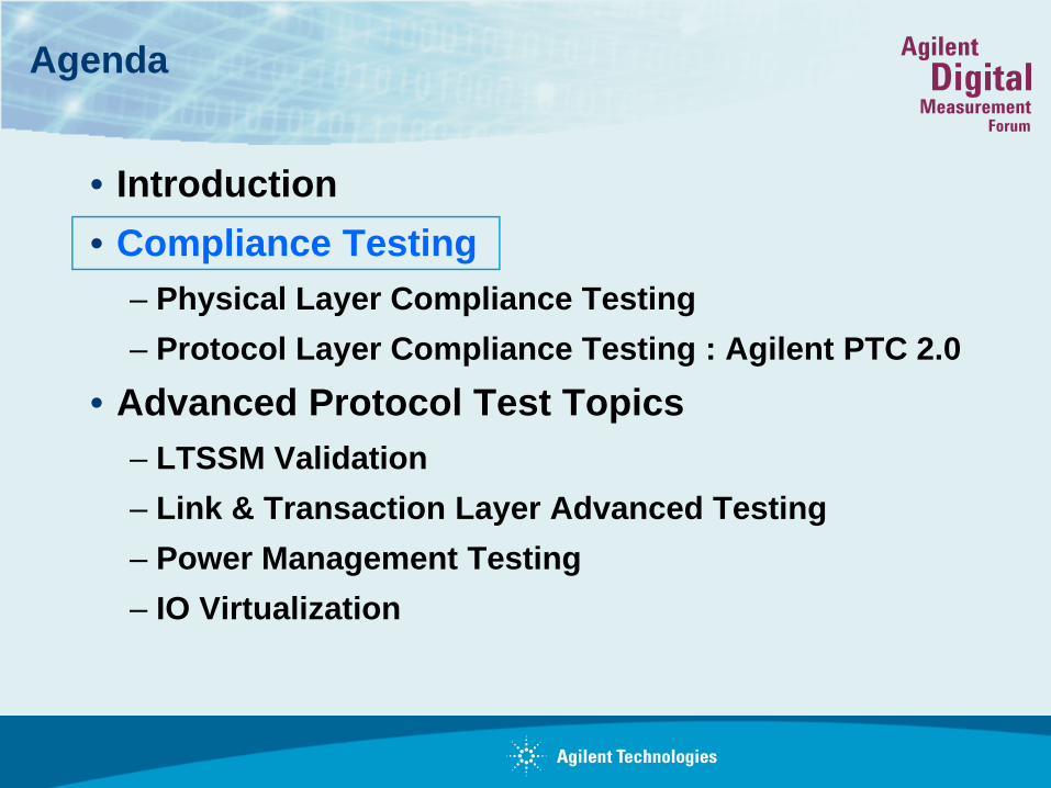
• Introduction• Compliance Testing
– Physical Layer Compliance Testing– Protocol Layer Compliance Testing : Agilent PTC 2.0
• Advanced Protocol Test Topics– LTSSM Validation– Link & Transaction Layer Advanced Testing– Power Management Testing– IO Virtualization
Agenda

• Introduction• Compliance Testing
– Physical Layer Compliance Testing– Protocol Layer Compliance Testing : Agilent PTC 2.0
• Advanced Protocol Test Topics– LTSSM Validation– Link & Transaction Layer Advanced Testing– Power Management Testing– IO Virtualization
Agenda

Testing and Validation
When using a standard technology such as PCI Express, detailed testing and validation is critical to ensure devices will interoperate with each other
Implementation of a proper test plan can significantly reduce cost later.
For example: How much does an ASIC spin cost when a bug is found after a device is in the field?
Introduction

Basic vs Advanced Testing Introduction
Basic Testing• PCI-SIG Compliance
Advanced Testing• From the Link Layer Test Specification
– “At this point this specification does not describe the full set of PCI Express tests for all link layer requirements. Going forward, as the testing gets mature, it is expected that more tests may be added as deemed necessary.”
• Ensuring your device is fully validated against the specifications
• Introduction• Compliance Testing
– Physical Layer Compliance Testing– Protocol Layer Compliance Testing : Agilent PTC 2.0
• Advanced Protocol Test Topics– LTSSM Validation– Link & Transaction Layer Advanced Testing– Power Management Testing– IO Virtualization
Agenda

PCI-SIG Compliance Testing
• Physical Layer– Validate Signal Quality of TX, Ref Clock and PLL Loop Bandwidth
• Configuration Space– Verify required fields and values behave as specified
• Link Layer & Transaction Layer– Exercise protocol, error and boundary layer conditions
• Platform Configuration– Validate BIOS correctly handles different topologies of PCI Express Devices
• Demonstrated Interoperability– Show that device drives load and device operates in actual PCI Express System
Introduction

• Introduction• Compliance Testing
– Physical Layer Compliance Testing– Protocol Layer Compliance Testing : Agilent PTC 2.0
• Advanced Protocol Test Topics– LTSSM Validation– Link & Transaction Layer Advanced Testing– Power Management Testing– IO Virtualization
Agenda

Physical Layer Testing Goals for PCIe 2.0
Goals for PHY testing are unchanged from PCI Express 1.0Achieving those goals is more challengingAdditional requirements added to increase confidence that designs are robustVerify designs achieve critical specification targets• Jitter• Eye mask• Reference Clock• Voltage and Jitter margining• Receiver Margining
Introduction

Changes Implemented under the 2.0 Specs- Physical Layer
Changes to the PCIe Base Specification• 5GT/s• Different de-emphasis levels• PLL bandwidth testing• Backward compatibility with PCIe 1.1
PCIe Card Electromechanical (CEM) Specification Changes• Rj / Dj tables and new jitter budgets• Changes to Reference clock phase jitter specification• 2 port measurement method for systems
2.0 changes

Signal Level and BW
2.5G de-emphasis = -3.5 +/- 0.5
5G de-emphasis = -3.5 +/- 0.5 OR -6.0 +/- 0.5
Low swing voltage levels = no de-emphasis
BW dependant peaking requirements• 3dB for 8 to 16MHz• 1dB for 5 to 8MHz• 2.5G same as 1.1
2.0 changes

PCIe 2.0 PLL Loop Bandwidth Testing External Ref Clock Input
Equipment Required:•Sine Wave Source (1GHz min)•Modulated Pulse Generator (100MHz)•Spectrum Analyzer (3 GHz min)•Modified CBB2
Steps:•Sweep source 100-125Mhz (-20dBM)•SA: 35KHz Res BW, 40MHz Span,
2.5 GHz center•Set display to peak hold•Normalize response to note 3dB point
Measure PLL BW
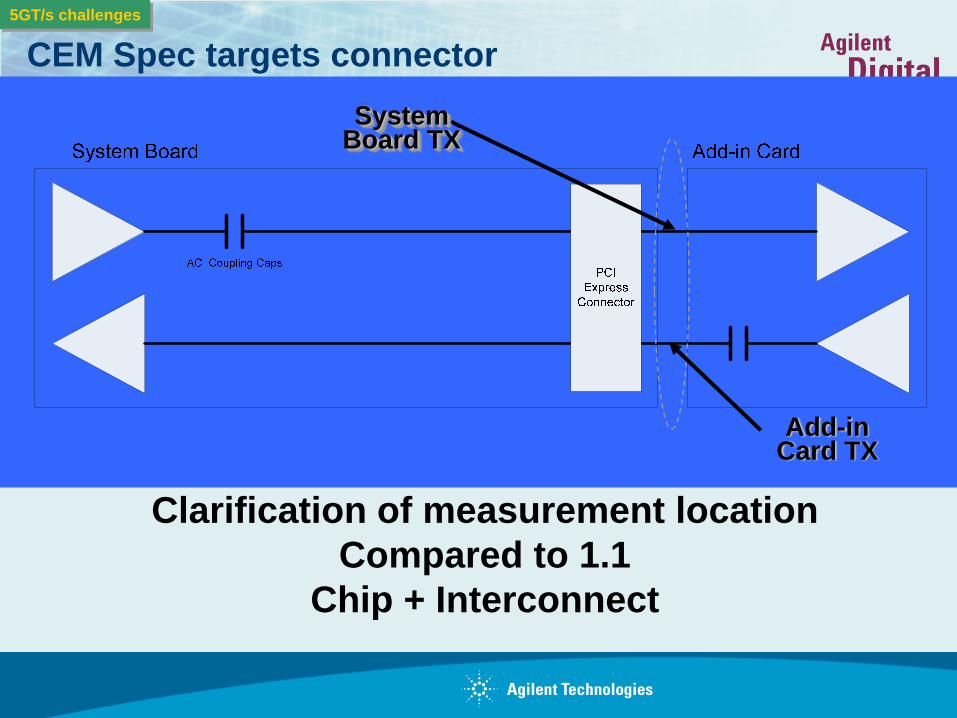
CEM Spec targets connectorSystem
Board TX
Add-in Card TX
Clarification of measurement locationCompared to 1.1
Chip + Interconnect
5GT/s challenges

Jitter measurement more complex!
Jitter decomposition required
Speed dependant phase jitter filters• 2.5G = 1 pole HPF• 5G = step band pass filter
Error correction needed to measure TX at pins
+/- 7.03For 10-12 BER
5GT/s challenges
5GT/s jitter challenges

De-embedding
New Transmitter base specification requirement- “Measurements at 5.0 GT/s must de-embed the test fixture- “It is also acceptable to use a common test fixture and de-
embed it for measurements at both 2.5 and 5.0 GT/s.”
What does it mean to de-embed?- “Measurement at 5.0 GT/s must de-convolve effects of
compliance test board to yield an effective measurement at Tx pins.”
Error Correction

Source of Measurement Inaccuracies• impedance mismatches• probing effects• smaller geometries• test cables and adapters• fixturing• device packaging, etc.• SCOPE NOISE FLOOR!
There are multiple ways to offset these measurement impairments.• calibration methods• mathematical signal processing• de-embedding/embedding techniques
Measurement system noise will be amplified by de-embedding techniques
Error Correction
Why is error correction neededto measure at TX pins?

Pre-measurement operations Post-measurement operations
De-embedding the CLB/CBBDSO91304A 13GHz Oscilloscope Calibrating the Scope
N5230A PNA-L Network Analyzer
Skew CalibrationProbe Attenuation/offset
Channel Vertical CalChannel Trigger Cal
S-parameters
Fixture effectsRemoved
Error Correction
Error Correction Techniques

Agilent Restricted
Page 18
PHYPHY
Tx Rx
Con
nect
or
Con
nect
or
Channel
• Compensate for Probing and Fixture Loss – Add Margin to Transmitter Characterization
• Allows more accurate measurement of de-emphasis levels at transmitter
• Compliance Requirement for Gen 2
Measured Waveform
De-embeddedWaveform
De-Convolve Function
Measured EyeDe-embedded Eye V
Error Correction
De-embedding –Loss Compensation or Gain Function
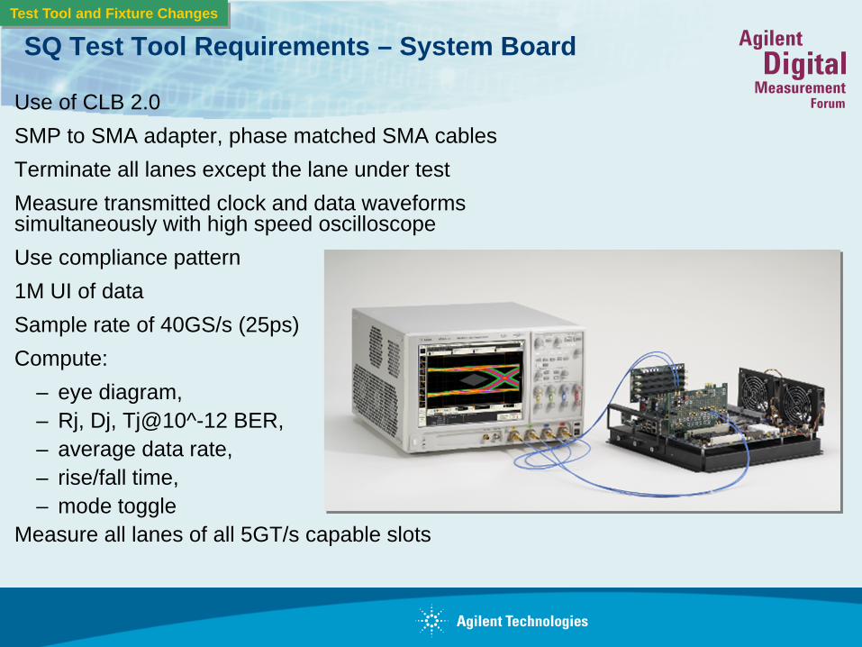
SQ Test Tool Requirements – System Board
Use of CLB 2.0SMP to SMA adapter, phase matched SMA cablesTerminate all lanes except the lane under testMeasure transmitted clock and data waveforms simultaneously with high speed oscilloscopeUse compliance pattern1M UI of dataSample rate of 40GS/s (25ps)Compute:
– eye diagram, – Rj, Dj, Tj@10^-12 BER, – average data rate, – rise/fall time, – mode toggle
Measure all lanes of all 5GT/s capable slots
Test Tool and Fixture Changes

Use of CBB 2.0SMP for all lanes, phase matched SMA cablesTerminate all lanes except the lane under testMeasure transmitted waveform with high speed oscilloscopeUse compliance pattern1M UI of dataSample rate of no more than 25 psCompute:
– eye diagram, – Rj, Dj, Tj@10^-12 BER, – average data rate, – rise/fall time, – mode toggle
Measure all lanes
Test Tool and Fixture Changes
Test Tool Requirements - AIC

Agilent Tools
What to Look for in PCI Express Compliance Automation
Key Requirements:- 1M UI automated data acquisition- Batch run capability for greater testing coverage or quick
spot checking- Implement measurements that respect the PCIe
Specification- Automated tools should self-scale to ensure top
accuracy for each measurement performed- Results must be consistent with PCI-SIG tools used at
Compliance Workshops

Test Results with the Agilent N5393BHTML based automatic report
generator allows you to easily share test results.
Select the version to test
Select the test point
Agilent Tools
• Introduction• Compliance Testing
– Physical Layer Compliance Testing– Protocol Layer Compliance Testing : Agilent PTC 2.0
• Advanced Protocol Test Topics– LTSSM Validation– Link & Transaction Layer Advanced Testing– Power Management Testing– IO Virtualization
Agenda
Logical Physical Layer testing
Link Training issues –
“I start link training but I cannot establish a link”
“I plugged my 1.1 card into a 2.0 system and it does not work, why?”
“I plugged my 2.0 card into a 1.1 system and it does not work”
“I pass electrical compliance but I still cannot link”
Although a card may successfully pass the electrical requirements, it may not be possible to link for other reasons.
This is critical for interoperability!
Protocol Test Considerations
Logical Physical Layer testing
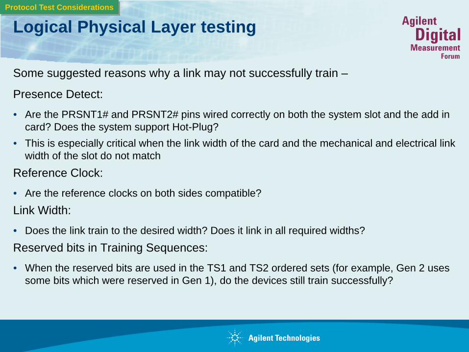
Some suggested reasons why a link may not successfully train –
Presence Detect:
• Are the PRSNT1# and PRSNT2# pins wired correctly on both the system slot and the add in card? Does the system support Hot-Plug?
• This is especially critical when the link width of the card and the mechanical and electrical link width of the slot do not match
Reference Clock:
• Are the reference clocks on both sides compatible?
Link Width:
• Does the link train to the desired width? Does it link in all required widths?
Reserved bits in Training Sequences:
• When the reserved bits are used in the TS1 and TS2 ordered sets (for example, Gen 2 uses some bits which were reserved in Gen 1), do the devices still train successfully?
Protocol Test Considerations
Electrical Testing vs. Protocol TestingProtocol Test Considerations
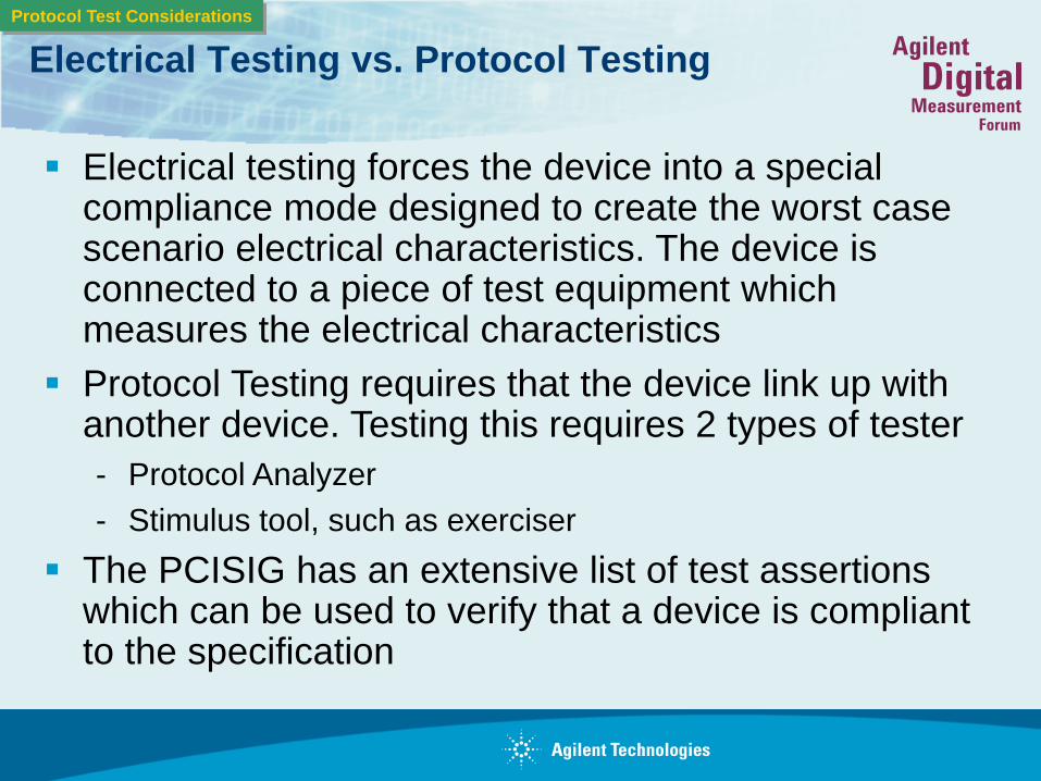
Electrical testing forces the device into a special compliance mode designed to create the worst case scenario electrical characteristics. The device is connected to a piece of test equipment which measures the electrical characteristicsProtocol Testing requires that the device link up with another device. Testing this requires 2 types of tester- Protocol Analyzer- Stimulus tool, such as exerciser
The PCISIG has an extensive list of test assertions which can be used to verify that a device is compliant to the specification

PCI-SIG Compliance
Goals for PCIe 2.0 Compliance Testing
Goals for Protocol testing are unchanged from PCI Express 1.0
Verify devices have met the critical specification targets for :• Config space test specification• Link layer test specifications• Transaction layer test specifications• Platform Bios test specifications
Additional testing regarding reserved bits usage

Link and Transaction Layer Testing
Test descriptions are not changed for Gen 2 Link and Transaction Layer tests with the exception of the Reserved bits test–
New for PCIe 2.0 devices • All Gen 2 devices will be tested at 2.5GT/s AND 5GT/s where appropriate• Gen 2, 2.5G only devices will be tested using the Gen 2 PTC• Reserved bits test tries to link up with all reserved bits set in training
sequences
PCI-SIG Compliance

Link and Transaction Layer Tests
Link Layer tests are a subset of the compliance checklist – a cross section of tests which if the device is compliant would indicate a reasonable chance of interoperability.
Includes Error checking, and dealing with Link stability problems
List of Link Layer and Transaction Layer Tests• BadLCRC • CorruptedDLLPs • DuplicateTLPSeqNum• LinkRetrainOnRetryFailNoAckNak• LinkRetrainOnRetryFail• ReXmitOnNak • ReplayNumTest • ReplayTLPOrder • ReplayTimerTest • RequestCompletion • ReserverdFieldsDLLPReceive• UndefinedDLLPEncoding• WrongSeqNumInAckDLLP
PCI-SIG Compliance

PCI-SIG Test Specification Documents
Test Number
Event the test checks for
Detailed description of the test case
PCI-SIG Compliance

Test Hardware Setup
Card being tested for compliance
Agilent PTC 2.0 approved by the
PCI-SIG for Protocol Gold Suite testing.
Agilent protocol analyzer for
troubleshooting any issues that come up
Agilent Tools

Agilent PTC II Software
1. Matching test case names to
easily identify which tests are
being run
2. Matching test
descriptions to the test spec.
5. Message framing to allow the analyzer to
easily capture the key parts of the test execution
3. Color coded to easily
identify what the test results
4. Report tab, with detailed
execution and reason for pass/fail
Agilent Tools

Testing the reserved bits in Training Sequences
In the 1.1 base specification, there are several reserved bits in the TS1 ordered set. Some of these bits are now used in the 2.0 specification – mainly in relation to the speed change and capability, in the Data Rate Identifier field:
1.1 Specification 2.0 Specification
2.0 Changes – Reserved Bit

Testing the Reserved Bits in Training Sequences
– It has been observed that many cards built to the 1.1 specification do not in fact ignore the reserved bits when used by a 2.0 device.
– This can cause the link not to train and is a severe interoperability issue
– The PCISIG has introduced an official test in the Link Layer test specification which ensures that devices can link when these reserved bits are used
– This test can be done with the Agilent Gen 2 PTC card or any of the Agilent Gen 2 Exerciser products
– Since official 1.1 testing will not change in the foreseeable future, this test can be run on 1.1 cards and is a very strong indicator whether the device will operate in a 2.0 system.
2.0 Changes – Reserved Bit

• Introduction• Compliance Testing
– Physical Layer Compliance Testing– Protocol Layer Compliance Testing : Agilent PTC 2.0
• Advanced Protocol Test Topics– LTSSM Validation– Link & Transaction Layer Advanced Testing– Power Management Testing– IO Virtualization
Agenda

2.0 Changes - LTSSM
Protocol Changes in the 2.0 Specs
Changes to the PCIe Base Specification• Physical Layer : Logical Sub Block
– 5GT/s Support– LTSSM use of Recovery state to Change to 5G speed– Link up/down configure – Dynamic Link Width change
• Data Link Layer– Replay timers for 5GT/s support
• Transaction Layer– Principally unchanged – the test specification is identical
• Configuration Space– Reserved bit usage, new registers to support different speed options

Two PCI Express devices exchange Training Sequences to negotiate link parameters like
lane polarity link numberset of lanes that belong to the linklane numbersscrambler enabled or disabledlink speednumber of fast training sequences required...
Training Sequences are also used to switch the link to low power states.
2.0 Changes - LTSSM
Device A
Device B
TS TS TS TS...
TS TS TS TS ...
How does link training work?
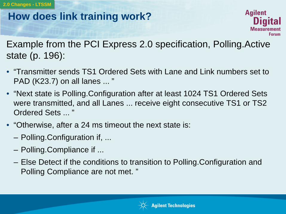
Example from the PCI Express 2.0 specification, Polling.Active state (p. 196):• “Transmitter sends TS1 Ordered Sets with Lane and Link numbers set to
PAD (K23.7) on all lanes ... ”• “Next state is Polling.Configuration after at least 1024 TS1 Ordered Sets
were transmitted, and all Lanes ... receive eight consecutive TS1 or TS2 Ordered Sets ... ”
• “Otherwise, after a 24 ms timeout the next state is:– Polling.Configuration if, ...– Polling.Compliance if ...– Else Detect if the conditions to transition to Polling.Configuration and
Polling Compliance are not met. ”
2.0 Changes - LTSSM
How does link training work?

What are the LTSSM test challenges?
The LTSSM with all its states, substates, transitions and conditions is quite complex. The number of possible scenarios is immense.Link training is a dynamic process. The sequence and timing of state transitions is not fixed. The sequence differs with
– different lane ordering– different timing behavior– signal integrity (occasional bit errors)– violations of the standard (error scenarios)– implementation specific behavior
LTSSM Test Challenges
New Challenges for Gen 2 – Speed Change!
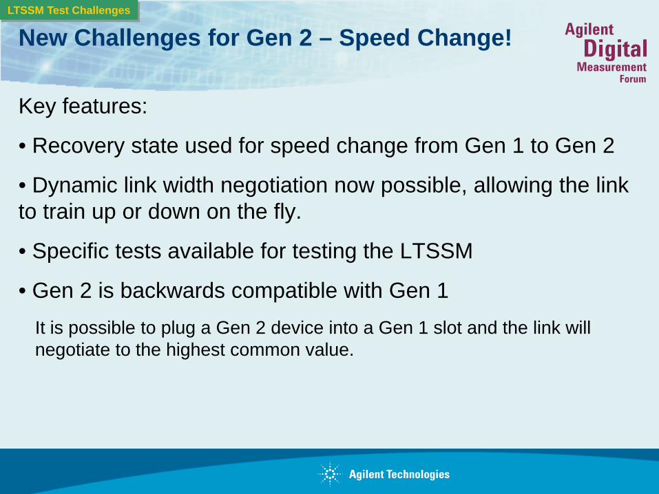
Key features:
• Recovery state used for speed change from Gen 1 to Gen 2
• Dynamic link width negotiation now possible, allowing the link to train up or down on the fly.
• Specific tests available for testing the LTSSM
• Gen 2 is backwards compatible with Gen 1It is possible to plug a Gen 2 device into a Gen 1 slot and the link will negotiate to the highest common value.
LTSSM Test Challenges

Agilent LTSSM TesterAgilent Tools

• Introduction• Compliance Testing
– Physical Layer Compliance Testing– Protocol Layer Compliance Testing : Agilent PTC 2.0
• Advanced Protocol Test Topics– LTSSM Validation– Link & Transaction Layer Advanced Testing– Power Management Testing– IO Virtualization
Agenda
Link & Transaction Layer Advanced Testing
• Large number of features/capabilities mandated by specification• Each requirement has many branches and many actions• Example : Advanced Error Reporting• Time consuming to create these test cases, and also time consuming to
troubleshoot and validate results
AER Test Challenges
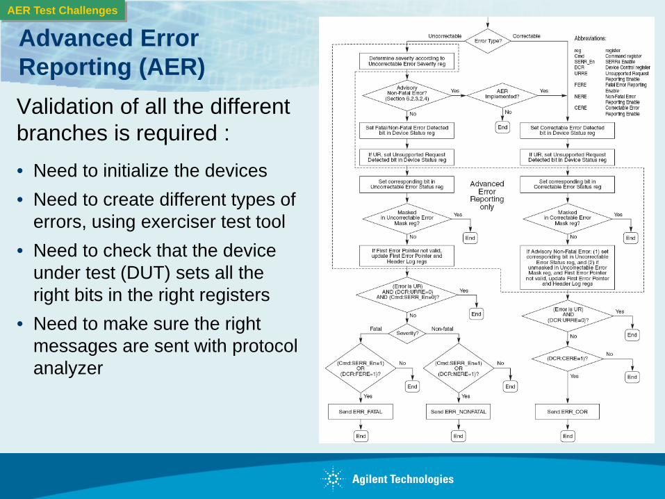
Advanced Error Reporting (AER)
AER Test Challenges
Validation of all the different branches is required :• Need to initialize the devices• Need to create different types of
errors, using exerciser test tool• Need to check that the device
under test (DUT) sets all the right bits in the right registers
• Need to make sure the right messages are sent with protocol analyzer

PTC II (E2969B) Compliance Assured Test Package (N5309A-COM)
Agilent Tools
PTC II (E2969B)• March 24, 2008 - Agilent Technologies Inc. today announced
that its Protocol Test Card (PTC) 2.0 has been approved by the PCI-SIG(r) (PCI Special Interest Group) for PCI Express(r) (PCIe(r)) 2.0 protocol testing.
• Includes all add-in card tests from the Gen1 PTC (22 tests)
• The Agilent PTC II will enable device compliance with the PCI-SIG® by providing 13 mandatory test cases.
• Upgradable to X1 exerciser in the future
Compliance Assured Test Package (N5309A-COM)• Compliance Assured Test Package (N5309A-COM), is available
and adds an additional 180 recommended tests. The Compliance Assured Test Package includes transaction layer, link layer, electrical layer and configuration space tests.
• Introduction• Compliance Testing
– Physical Layer Compliance Testing– Protocol Layer Compliance Testing : Agilent PTC 2.0
• Advanced Protocol Test Topics– LTSSM Validation– Link & Transaction Layer Advanced Testing– Power Management Testing– IO Virtualization
Agenda

What is Power ManagementIntroduction
Power savings by going into low power statesState Description Recovery
TimeL0 Fully Active N/A
L0s Standby ns
L1 Low Power Standby
us
L2 Low Power Sleep
ms
L3 Off (zero power)
ms

Power Management (ASPM) Testing
Drivers :
• Windows Vista supports the low power states for medium power saving and high power saving modes
• Cost savings in terms of power consumption, heating/cooling in datacenters
• Drive towards green devices
Challenges :• Many devices have problems going in and out of the electrical idle states
L0s and L1• The link is technically still active in these cases even although it is in
Electrical idle• Getting devices into these low power states on demand, and waking them
up on demand
Test Challenges

Power Management TestingAgilent Tools
Exerciser • L0s support; ensure one
direction only goes into L0s• L1 support
– Trigger other device to enter into L1 state
Analyzer • PM packet decodes• Fast sync times to track
devices going into and out of PM states

• Introduction• Compliance Testing
– Physical Layer Compliance Testing– Protocol Layer Compliance Testing : Agilent PTC 2.0
• Advanced Protocol Test Topics– LTSSM Validation– Link & Transaction Layer Advanced Testing– Power Management Testing– IO Virtualization
Agenda

What is I/O Virtualization
I/O Virtualization (IOV) – The capability for a single physical I/O unit [e.g. NIC card] to be shared by more than one system
image (SI).
SR-IOV : Single Root IOV
MR-IOV : Multi Root IOV
Standards are an overlap, however, application drivers for SR-IOV and MR-IOV are very different
New Specs - IOV

SR-IOV Drivers
Better server utilization through :• Software virtual machines on one
physical server ; VMWare, Parallels, etc
• I/O end points does not need to know about virtualization
Challenges of current technology• Requires software/firmware
intermediary • The intermediary is involved in all
transactions; configuration, I/O transfers, which lowers the performance
2.0 Changes - IOV

MR-IOV Drivers
Cost reduction• I/O Purchase cost :each blade
server goes from 28 NIC cards and 4 switches to 4 NIC cards and 2 switches
• Cost of power and cooling to the data center
• IO Consolidation : Moving from multiple technologies to single -> Ethernet & FC to FCoE
Server FCEnet
Server FCEnet
Server FCEnet
….
Ene
t Sw
itch
Ene
t Sw
itch
FC S
witc
h
FC S
witc
h
Server
Server
Server
….
RC
RC
RC
PC
Ie S
witc
h
PC
Ie S
witc
h
FCoE
Current blade server
I/O consolidated blade server
FCoE
2.0 Changes - IOV

MR-IOV on Protocol AnalyzerAgilent Tools
MR-IOV fields decoded for easy
analysis

The Digital Application
Logic Analysis SolutionFSBMemory BusGeneral Purpose
The Agilent E2960B Series for PCI Express® 2.0 Unique In The Industry
Agilent PCI Express® 1.0 & 2.0 Solution
API – Automation
Protocol AnalyzerPacket, transaction and
payload viewsEasy flow technologyAdvanced Triggering
Protocol Analysis SolutionFibre ChannelPCI ExpressASI
Lane AnalyzerPer-lane display8B/10B decodeTriggering on ordered setPower Management
One Analyzer – Two Use Models
ProbingMidbus 2.0 x16Interposer x16
ExerciserLTSSM x16
X16 Device Emulation & Error Insertion
Compliance Testing
ExtendedP2L gateway
Agilent Tools

For further information
You will find more information on PCI Express 2.0 and Agilent solutions for PCI Express at:
.
www.pci-sig.com PCI-SIG Website, Specification, S/W Tools, Agilent Test Procedure
www.agilent.com/find/ptc2 Agilent Protocol Test Card 2.0 (PTCII) for Protocol Compliance Testing
www.agilent.com/find/pciexpress Agilent tools to help you succeed with your PCI Express design such as the N5393A Compliance application.
www.agilent.com/find/pcie2 Agilent PCI Express 2.0 Protocol Test Solutions
www.agilent.com/find/si Agilent tools to help you master signal integrity challenges
![[Compliance Presentation Title/Subject] · function. Compliance Testing is the independent testing arm of the Citi Compliance function. Our mission is to: Compliance Testing plans](https://img.dokumen.tips/doc/110x75/5e47b61e9e5ff6667e3cd0eb/compliance-presentation-titlesubject-function-compliance-testing-is-the-independent.jpg)