Embed Size (px)
Citation preview

Advanced Micro Devices
An Emulation of the Am9080A
An Example ofA Microprogrammed Machine
By Moshe Shavit
Copyright © 1978 by Advanced Micro Devices, Inc.
Advanced Micro Devices cannot assume responsibility for use of any circuitry described other than circuitry entirely
• embodied in an Advanced Micro Devices' product.
AMPUB-064

TABLE OF CONTENTS
INTRODUCTION .
GENERAL PHILOSOPHYThe Architecture .The Microprogram Control Unit .
THE HARDWAREBus Interface and Interrupt Control 6Microprogram Memory 6ALU and Working Registers 7InstructionDecode. . . . . . . . . . . . . . . . . . . . . . . . . . . . . . . . . . . . . . . . . . . . . . . . . . . . . . . . . . . . . . . . . . . .. 8Status Bits . . . . . . . . . . . . . . . . . . . . . . . . . . . . . . . . . . . . . . . . . . . . . . . . . . . . . . . . . . . . . . . . . . . . . . . . . . .. 8Timing Considerations 9
THE MiCROCODE 10
SUMMARy 11
PARTS LIST , 11
APPENDIX I A-1
APPENDIX II A-5
APPENDIX III A-28

INTRODUCTION
The Am2901 A Four-Bit Bipolar Microprocessor Slice and itsassociated support circuits have become the industry standard. However, even as this niche is already carved in themicroprocessor industry, consideration must also be made tothose users who either have not dealt with the speed and flexibility of the Am2900 Family or have utilized other types ofmicroprocessing in their applications. Therefore, it is importantthat the needs of these users be met at least partially by allowing them to adapt to this new concept through the use offamiliar tools.
This document describes the emulation of an Am9080AEight-Bit MOS Microprocessor built around four Am2901 A BitSlices and three Am2909 Microprogram Sequencers. Theprimary purposes of this design are:
1. To demonstrate the use of the Am2901 A, Am2909, andmicroprogramming in general, and
2. To emulate the Am9080A/Am8228 chip set in such a wayas to better enable the user to make the transition to implementing the Am2900 Family in his system, particularly ifhe has previously been Am9080A-oriented.
The design was not intended to minimize component count orcycle times, but rather to demonstrate an emulation in themost straightforward manner. However, even though speedwas not the first consideration in this design, the emulatorneeds, on the average, about 40O/C fewer clock cycles thandoes the Am9080A (see Table 1). Also, it can run with amaximum clock frequency of about 5MHz, which altogether isabout a 4:1 speed improvement over the standard 2MHzAm9080AlAm8228 instruction set (see Table 7).
Furthermore, the emulator has the same input/output linesand controls as does the Am9080A/Am8228 set, i.e.:
1. A 16-bit wide Address Bus2. An 8-bit wide Data Bus3. MEMR, MEMW, I/OR, I/OW, HLDA, WAIT and INTA con-
trol outputs4. HOLD, READY, INT, and RESET control inputs.
A complete list of the parts used in this design can be foundat the end of the text.
GENERAL PHILOSOPHY
The Architecture
The heart of the emulator is a 16-bit wide ALU constructedwith four Am2901 A Four-Bit Bipolar Microprocessor Slices.Their internal registers are assigned as the Am9080A registers, inclUding both the Program Counter and the StackPointer. The four Am2901A's are grouped in two pairs, a HighOrder Pair and a Low Order Pair. This scheme provides aneasy access to the 16-bit register pairs (B-C, D-E, H-L) aswell as to the 16-bit registers (PC, SP). The internal registerallocations of the Am2901A's are depicted in Table 2. Notethat for the High Order Pair (HOP), the Am2901 A memory locations for each of the working registers are the same as thenumbers used to identify these registers as source or destination registers in the Am9080A instructions. Thus, by properlydecoding these bits in the Am9080A instructions and applyingthem to the A or B addresses of the Am2901 A's, all of theAm9080A register-to-register instructions (approximately 25%of the total number of instructions) can be handled by onlyone set of microinstructions. This, of course, simplifies andshortens the microprogram.
Furthermore, addressing a register pair (B-C, D-E, H-L) ismade easy by selecting bits 4 and 5 of the Am9080A instruction and applying them to the A or B address of theAm2901 A's. This is true provided the register in the LowOrder Pair (LOP) contains the same data as its correspondingregister in the HOP. It can be accomplished merely by inverting the Least Significant Bit of the LOP register addresswhenever a single-byte (8-bit) operation is performed. Forexample, if the Am9080A instruction INR B (Increment Register B) is to be performed, its destination bits (000) are appliedto the HOP B addresses, addressing Register O. However,001 is applied to the LOP B address, addressing Register 1,which again is B.
Executing double register operations (INX, DCX, LXI, etc.)does not require this Least Significant Bit (LSB) inversion, butfor these instructions, the adjacent pairs of registers shouldalways be updated. This can be accomplished by byteswapping, e.g. taking Register H from the HOP (No.4) andwriting its contents into Register H of the LOP (No.5), and atthe same time taking Register L from the LOP (No.4) andwriting its contents into Register L of the HOP (No.5). All ofthis can be done in one microcycle, and as the amount ofsuch instructions is relatively small, the time consumption involved is negligible.
This system of register allocation uses only 3 bits of the microinstruction, but shortens by an appreciable amount both themicrocode and the execution times. The registers adjacent tothose allocated to A, PC, and SP are used as "scratchpads".The constants in Registers 12 and 13 are loaded in the initialization phase following a restart and are used in the restartinstruction (RST) to properly mask the restart address bitsfrom the Data Bus.
The Microprogram Control Unit
Figure 1 is a block diagram of the Microprogram Control portion of the emulator. This unit is a typical example of a computer control unit that uses three Am2909 MicroprogramSequencers. In an instruction fetch cycle, the Instruction Register latches the instruction appearing on the Data Bus and retains it during its execution. The output of this register isapplied to the Mapping PROM (256 words by 12 bits) addressinputs. This PROM maps the 8-bit instruction into the appropriate 12-bit microprogram memory address. The data ouputsof this Mapping PROM are connected to the D inputs of theAm2909's. Some Instruction Register bits also go to the ALUfor register selection.
The Am2909 control lines are controlled by a SequencePROM. Three of the Sequence PROM address inputs comefrom the Pipeline Register and a fourth is supplied by asixteen-input Condition Code Multiplexer. Of its sixteen inputs,twelve are used: five for the Am9080A flags (CY, Z, S, P,AC), three for the micro-status bits (F=O, F3, Cn+4), three forthe INT, READY, and HOLD controls to the emulator, and onealways TRUE input which the sequencer uses to execute aninstruction unconditionally. The interrupt inputs are gated withone bit from the Sequence PROM and connected to theAm2909 OR inputs. This effectively allows the forcing of "1 "'sinto all of the OR inputs of the Am2909's when an interrupt isrequested, while at the same time enabling the interrupt, forcing "1 '''s into all of the microprogram address lines. At thehighest available microprogram address, there is a JUMP tothe interrupt handler.

Table 1. Clock Cycle Requirements for the Am9080A Emulation.
blAClock Cycles
N beOp Code
um r I ssem y I I
Of Bytes I Am9080AAm9080A
IMnemonic I
Instruction Description07 0 6 0 5 0 4 0 3 O2 0 1 DO Emulation*
DATA TRANSFER
0 1 d d d s s s 1 5 3 MOVr, r Move register to register0 1 1 1 0 s s s 1 7 5 MOVm, r Move register to memory0 1 d d d 1 1 0 1 7 5 MOVr, m Move memory to register0 0 d d d 1 1 0 2 7 5 MVI, r Move to register, immediate0 0 1 1 0 1 1 0 2 10 7 MVI,m Move to memory, immediate0 0 1 1 1 0 1 0 3 13 4 LDA Load Ace, direct0 0 0 0 1 0 1 0 1 7 5 LDAXB Load Ace, indirect via B & C0 0 0 1 1 0 1 0 1 7 5 LDAXD Load Ace, indirect via D & E0 0 1 0 1 0 1 0 3 16 12 LHLD Load H & L, direct0 0 1 0 0 0 0 1 3 10 5 LXI H Load H & L, immediate0 0 0 1 0 0 1 1 3 10 5 LXID Load D & E, immediate0 0 0 0 0 0 0 1 3 10 5 LXI B Load B & C, immediate0 0 1 1 0 0 0 1 3 10 5 LXI SP Load stack pointer, immediate0 0 1 0 0 0 1 0 3 16 11 SHLD Store H & L, direct0 0 1 1 0 0 1 0 3 13 9 STA Store Acc, direct0 0 0 0 0 0 1 0 1 7 5 STAX B Store Ace, indirect via B & C0 0 0 1 0 0 1 0 1 7 5 STAX D Store Ace, indirect via D & E1 1 1 1 1 0 0 1 1 5 3 SPHL Transfer H & L to stack pointer1 1 1 0 1 0 1 1 1 4 5 XCHG Exchange D & E with H & L1 1 1 0 0 0 1 1 1 18 11 XTHL Exchange top of stack with H & L1 1 0 1 1 0 1 1 2 10 6 IN Input to Ace1 1 0 1 0 0 1 1 2 10 5 OUT Output from Acc
CONTROL
0 1 1 1 0 1 1 0 1 7 I 6 HLT Halt and enter wait state0 0 1 1 0 1 1 1 1 4 3 I STC Set carry flag0 0 1 1 1 1 1 1 1 4 4-3 CMC Complement carry flag1 1 1 1 1 0 1 1 1 4 3 EI Enable interrupts1 1 1 1 0 0 1 1 1 4 3 DI Disable interrupts0 0 0 0 0- 0 0 0 1 4 :5 NO? No operation
BRANCHING
1 1 0 0 0 0 1 1 3 10 7 JMP Jump unconditionally1 1 0 1 1 0 1 0 3 10 8-5 JC Jump on carry1 1 0 1 0 0 1 0 3 10 8-5 JNC Jump on no carry1 1 0 0 1 0 1 0 3 10 8-5 JZ Jump on zero1 1 0 0 0 0 1 0 3 10 8-5 JNZ Jump on not zero1 1 1 1 0 0 1 0 3 10 8-5 JP Jump on positive1 1 1 1 1 0 1 0 3 10 8-5 JM Jump on minus1 1 1 0 1 0 1 0 3 10 8-5 JPE Jump on parity even1 1 1 0 0 0 1 0 3 10 8-5 JPO Jump on parity odd1 1 0 0 1 1 0 1 3 17 11 CALL Call unconditionally1 1 0 1 1 1 0 0 3 17-11 12-5 CC Call on carry1 1 0 1 0 1 0 0 3 17-11 12-5 CNC Call on no carry1 1 0 0 1 1 0 0 3 17-11 12-5 CZ Call on zero1 1 0 0 0 1 0 0 3 17-11 12-5 CNZ Call on not zero1 1 1 1 0 1 0 0 3 17-11 12-5 CP ! Call on positive1 1 1 1 1 1 0 0 3 17-11 12-5 CM Call on minus1 1 1 0 1 1 0 0 3 17-11
I
12-5 CPE I Call on parity even1 1 1 0 0 1 0 0 3 17-11 I 12-5 CPO Call on parity odd1 1 0 0 1 0 0 1 1 10 8 RET Return unconditionally1 1 0 1 1 0 0 0 1 11-5 9-3 RC Return on carry1 0 1 0 0 0 0 11-5 9-3 RNC Return on no carry
I 1 0 0 1 0 0 0 11-5 9-3 RZ Return on zero1 0 0 0 0 0 0 11-5 9-3 RNZ Return on not zero1 1 1 0 0 0 0 11-5 9-3 RP Return on positive1 1 1 1 0 0 0 11-5 9-3 RM Return on minus1 1 0 1 0 0 0 11-5 9-3 RPE Return on parity even1 1 0 0 0 0 0 11-5 9-3 RPO Return on parity odd1 1 0 1 0 0 1 5 3 PCHl Jump unconditionally,
indirect via H & LV V V 11 9 RST Restart
-The oomber of clock cycles required to execute some instructions may vary, according to the conditions present at execution time. For example,aCMe (CompIemenl Carry) j& in'IpIem8nted in microcode, not in hardware. The carry is uncondi&ionaIIy reset while the pr,QIIKlus SUiws of this flagis examined. If it was already reset, a jump to the STC (Set Carry) routine is performed; otherwise, the next instruction is immediately fetched.
2

Table 1. Clock Cycle Requirements for the Am90BOA Emulation. (Cont.)
Subtract from Acc, ImmediateSubtract with borrow from
Acc, immediateDecimal adjust Acc
SUISBI
DAA
46-5
20-84
77
---4-
STACK OPERATIONS
11 6 PUSH B Push registers B & C on stack11 6 PUSH D Push registers D & E on stack11 6 PUSH H Push registers H & L on stack11 8 PUSH PSW Push Acc and flags on stack10 8 POP B Pop registers B & C off stack10 8 POP D Pop registers D & E off stack10 8 POP H Pop registers H & L off stack10 8 POP PSW Pop Acc and flags off stack
LOGICAL
4 3 ANA r AND register with Acc7 5 ANA m AND memory with Acc7 4 ANI AND with Acc, immediate4 3 XRA r Exclusive OR register with Acc7 5 XRA m Exclusive OR memory with Acc7 4 XRI Exclusive OR with Acc, immediate4 3 ORAr Inclusive OR register with Acc7 5 ORAm Inclusive OR ~emory with Acc7 5 ORI Inclusive OR with Acc, immediate4 3 CMPr Compare register with Acc
22
oo
o1
oo
0 0 0 0
0 0 0 1 00 1 0 1 01 0 0 1 01 1 0 1 00 0 0 0 00 1 0 0 01 0 0 0 01 1 0 0 0
0 0 0 s s s 10 0 0 1 1 0 11 0 0 1 1 0 20 0 1 s s s 10 0 1 1 1 0 11 0 1 1 1 0 20 1 0 s s s 10 1 0 1 1 0 11 1 0 1 1 0 20 1 1 s s s 1
Op Code Clock Cycles !
INumber Am9080A I Assembly Instruction DescriptionOf Bytes Am9080A
IMnemonic I0 7 0 6 05 0 4 0 3 O2 0 1 Do Emulation
1
ARITHMETIC I
II
1 0 0 0 0 s s s 1 4 3!
ADDr Add register to Acc1 0 0 0 1 s s s 1 4 4 I ADCr Add with carry register to Acc1 0 0 0 0 1 1 0 1 7 5 i ADDm I Add memory to Acc1 0 0 0 1 1 1 0 1 7 5
IADCm
I
Add with carry memory to Acc1 1 0 0 0 1 1 0 2 7 4 ADI Add to Acc, immediate1 1 0 0 1 1 1 0 2 7 5 I ACI I Add with carry to Acc, immediate
! I0 0 0 0 1 0 0 1 1 10 4 ! DAD B
iDouble add B & C to H & L
0 0 0 1 1 0 0 1 1 10 4 1 DAD D I Double add D & E to H & L0 0 1 0 1 0 0 1 1 10
I
4 ! DAD H i Double add H & L to H & Li !0 0 1 1 1 0 0 1 1 10 4 DAD SP Double add stack pointer to H & L
1 0 0 1 0 s s s 1 4 I 3 I SUBr
I
Subtract register from Acc1 0 0 1 1 s s· s 1 4 I 4 I SBBr Subtract with borrow register
I ! from Acc1 0 0 1 0 1 1 0 1 7
!5 I SUBm i Subtract memory from Acc
1 0 0 1 1 1 1 0 1 7 1 5I
SBBmI Subtract with borrow memory
1 from AccI
1 0 1 1 1 1 1 0 1 7 5 CMP. m Compare memory with Acc1 1 1 1 1 1 1 0 2 7 4 CPI Compare with Acc, immediate0 0 1 0 1 1 1 1 1 4 3 CMA Complement Acc0 0 0 0 0 1 1 1 1 4 5-4 RLC Rotate Acc left0 0 0 0 1 1 1 1 1 4 6-5 RRC Rotate Acc right0 0 0 1 0 1 1 1 1 4 5-4 RAL Rotate Acc left through carry0 0 0 1 1 1 1 1 1
,4 6-5 RAR Rotate Acc right through carry
INCREMENT/DECREMENT
0 0 d d d 1 0 0 1 5 3 INR r Increment register0 0 1 1 0 1 0 0 1 10 6 INR m Increment memory0 0 0 0 0 0 1 1 1 5 4 INX B Increment extended B & C
I 0 0 0 1 0 0 1 1 1 5 4 INX D Increment extended D & E
I0 0 1 0 0 0 1 1 1 5 4 INX H Increment extended H & L
! 0 0 1 1 0 0 1 1 1 5 4 INX SP Increment stack pointer0 0 d d d 1 0 1 1 5 3 DCR r Decrement register0 0 1 1 0 1 0 1 1 10 6 DCR m Decrement memory0 0 0 0 1 0 1 1 1 5 4 DCX B Decrement extended B & C0 0 0 1 1 0 1 1 1 5 4 DCX D Decrement extended D & E0 0 1 0 1 0 1 1 1
i
5 4 DCX H Decrement extended H & L0 0 1 1 1 0 1 1 1 5 4 DCX SP Decrement stack pointer
3

A a// DATA BUS BUSO-BUS7
'I / fa aMICROPROGRAM
CP IN~~~~~~~NCONTROLLED
I 6
fa SOURCE &DESTINATIONADDRESS TO
MAPPING Am2901A'S
PROM
12 I
f27 14 R D
r+- SEQUENCE3 X Am2909PROM
~OR Y
" INT. ENABLE 1f2~
" INT. REG.I
15MICROPROGRAM
MEMORY
FROM STATUSCONDITIONAND CONDITION --r12 +44REGISTERS CODE
MUX
~VCC MICROPROGRAM
I_DIRECT DATA ICONTROLLED PIPELINE
POLARITY -IOE REGISTER REGISTER
-1-a 4-1- 401OTHER
I FUNCTIONS
MPR-428
Figure 1. Microprogram Control Unit.
Table 2.
Am9080A Emulation Register Allocations.
Am2901A High LowRegister # Order Pair Order Pair
0 B C
1 C B
2 D E
3 E D
4 H L
5 L H
6 not used A
7 A not used
8 not used not used
9 Stack Pointer Stack Pointer
10 scratch pad scratch pad
11 scratch pad scratch pad
12 00000000 00111000
13 00111000 0000000014 not used not used
15 Program Coumer Program Counter
4
The microprogram memory is organized as 56 bits wide and352 words deep. Twelve of the fifty-six bits of the microprogram word are used to supply the address of the next microinstruction if a jump is needed in the microcode. The eightleast significant bits of this field can also be applied (undermicroprogram control) to the Data Bus, thus allowing theAm2901 A's to obtain data from the microinstruction. Threebits of the microprogram word are needed for the SequencePROM and one bit is used to control the Condition Code Multiplexer polarity. The remaining forty bits are used in the ALUand in the other parts of the emulator.
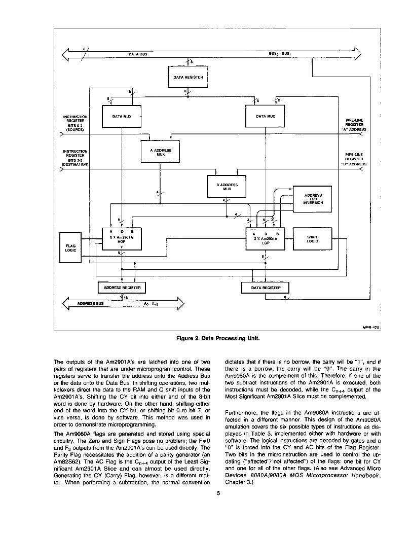
Figure 2 is a block diagram showing the connections for theregister, address, and data inputs of the Am2901 A's. Dataappearing on the Data Bus is latched into the Data Register.Supplying data to each pair of Am2901 A's is a Data Multiplexer which can select either the output of the Data Registeror, if a byte swap is to be performed, the output of the opposite pair of Am2901 A's. The A and B address multiplexerschoose between the register addresses supplied by the microinstruction and those extracted from the Am9080A instruction.Within the s~tem. as was earlier desclibed. LSB il1Yel"Sioncircuitry allows single-or double-byte addressing on the LOP.
A 8/ :>/ DATA BUS BUSo BUS7
" I {'8V
DATA REGISTER
8} *~ ~ --::r8 18
INSTRUCTION DATA MUX DATA MUXREGISTER PIPE-LINE
BITS D-2 REGISTER(SOURCE) "A" ADDRESS....
" • +
INSTRUCTION A ADDRESSREGISTER MUX PIPE-LINE
BITS 3-5 REGISTER
(DESTINATION) "B" ADDRESS-'"
• t
B ADDRESSMUX ".---
~,,- ,;-- ADDRESS4 LSB
INVERSION
4" (81--- ! " 3 1 ~ " 3j.--,,-
A D BA D B
2 X Am2901A 2 X Am2901A I- SHIFT f- -- HOP
ILOP LOGIC
FLAG yLOGIC
88,,-
1t
I ADDRESS REGISTER 1 .1 DATA REGISTER IA 116 '" 8
ADORESSBUS Ao-A15
'" V
MPR-429
Figure 2. Data Processing Unit.
The outputs of the Am2901 A's are latched into one of twopairs of registers that are under microprogram control. Theseregisters serve to transfer the address onto the Address Busor the data onto the Data Bus. In shifting operations, two multiplexers direct the data to the RAM and Q shift inputs of theAm2901A's. Shifting the CY bit into either end of the 8-bitword is done by hardware. On the other hand, shifting eitherend of the word into the CY bit, or shifting bit 0 to bit 7, orvice versa, is done by software. This method was used inorder to demonstrate microprogramming.
The Am9080A flags are generated and stored using specialcircuitry. The Zero and Sign Flags pose no problem; the F;=Oand F3 outputs from the Am2901A's can be used directly. TheParity Flag necessitates the addition of a parity generator (anAm82S62). The AC Flag is the Cn+4 output of the Least Significant Am2901 A Slice and can almost be used directly.Generating the CY (Carry) Flag, however, is a different matter. When performing a subtraction, the normal convention
5
dictates that if there is no borrow, the carry will be "1", and ifthere is a borrow, the carry will be "0". The carry in theAm9080A is the complement of this. Therefore, if one of thetwo subtract instructions of the Am2901 A is executed, bothinstructions must be decoded, while the Cn+4 output of theMost Significant Am2901 A Slice must be complemented.
Furthermore, the flags in the Am9080A instructions are affected in a different manner. This design of the Am9080Aemulation covers the six possible types of instructions as displayed in Table 3, implemented either with hardware or withsoftware. The logical instructions are decoded by gates and a"0" is forced into the CY and AC bits of the Flag Register.Two bits in the microinstruction are used to control the updating ("affected"/"not affected") of the flags: one bit for CYand one for all of the other flags. (Also see Advanced MicroDevices' BOBOA/90BOA MOS Microprocessor Handbook,Chapter 3.)

Table 3. Am9080A Flags. Table 4. Microcode Bit Allocation Summary.
• This notation is used in the text to indicate a certain pin of the devicebaing referenced. Hence, ill this case, the text is talking about pin 8 ofU7S.
INR, DCR NA A A
DAD, CMC, STC, all Rotates A NA NA
ORA, ORI, XRA, XRI C C A
ANA, ANI C ND A
{ either A A AOther instructions
or NA NA NA
Microprogram Memory
The microprogram memory can be any memory array providing 56-bit wide words 352 words deep. Using sevenAm29773 512 x 8 PROM's for this arrangement will provide atypical 45ns access time, although other configurations arepossible. Table 4 is a summary of the microcode bit allocation. Some of the microprogram memory data are stored inthe Pipeline Registers, made up of seven Am25LS374 eight-
THE HARDWARE
Bus Interface and Interrupt Control
Figure 3 depicts in detail the sequencing portion of theAm9080Aemulation. The Data Bus, comprised of BUSothrough BUS7 , is connected to the inputs of an Am25LS377eight-bit Register (U1516). Data appearing on the Data Bus isclocked into this register if its E input is LOW, which normallyhappens during an instruction fetch cycle. The instruction thusstored in this register is now available on the output of theregister during the entire execution time, both for the MappingPROM's (three Am29761: U11, U12, U13) and for the Register Address Multiplexers (two Am25LS157: U65. U66 in Figure 4). The Mapping PROM's supply addresses to the 0 inputs of the three Am2909 sequencers (U21, U22, U23),whose R inputs are connected to the microprogram memoryoutput (bits }L42-}L53). Since the RE inputs of the sequencersare always LOW, their internal registers serve as a part of thePipeline Register. They will contain the next microprogramaddress if a jump is anticipated. The So, S1' PUP, and FEcontrol inputs of the sequencers are driven by a SequencePROM, an Am29751 (U14), and their CPU inputs are drivenby the system clock. The least significant Cn input is tied toHIGH, while the remaining Cn inputs are driven by the preceding Cn+4' The ZERO inputs are normally pulled HIGH, but amomentary push-button can force a LOW, thus steering themicroprogram to Location 0 for initialization. All of the OR inputs of the sequencers are tied together and to the output ofan AND gate (8/U73*). If the interrupt is enabled (INTE=HIGH), and there is an interrupt request (INT=HIGH),and the Do output of the Sequence PROM is also HIGH, thenthe highest available location of the microprogram memorywill be addressed where a "Jump-to-Interrupt Handler" instruction is written. Using the 0 0 output of the SequencePROM to gate interrupts provides a simple means to assurethat an interrupt can be executed only at macroinstructionboundaries. This is achieved by setting this bit LOW in everymicroinstruction except in the instruction fetch, where it isHIGH. The Y outputs of the sequencers, always enabled,supply the microcode memory address.
I No of II Bit No. I Description I
Bits
0-2 3 ALU Source (10.12 of the Am2901 A's)
3·5 3 ALU Function (Is-Is of the Am2901 A's)
6-8 3 ALU Destination (16-18 of the Am2901A's)
9-12 4 ALU "B" Address
13·16 4 ALU "A" Address
17 1 Single/Double Byte
18 1 Cn for least significant Am2901A slice
19 1 Rotate and Swap Control (formatted)
20-21 2 Update/keep flags
22 1 "A" Address Switch
23-24 2 Am2901 A Output Steering Control
25-26 2 Data Bus Enable Control
27-32 6 HLDA, MEMW, MEMR, I/OW, IIOR, INTAAm9080A System Control Outputs
33 1 "B" Address Switch
34-37 4 Condition Code Select
38 1 Condition Code Polarity Control
39-41 3 Next Instruction Select
42-5-3 12 Numerica! Field
54 1 Numerical Field to Data Bus Control
55 1 Instruction Register Clock Enable
bit Registers (U3132, U3241 , U4142, U51, U8182, U7172,U5161). The microinstructions are comprised of the outputs ofthese devices, each output being designated "PL". Five ofthese registers have their outputs constantly enabled. This allows the microinstruction to be delivered to the various partsof the circuit. Bit PL27 serves a dual purpose in this part ofthe circuit. Besides controlling the output of U7172, it is alsoinverted to serve as the HLDA output control line. This latterfunction allows the floating of all of the control outputs, exceptHLDA, when a Hold is acknowledged.
The output of U8182 is connected to the Data Bus and is enabled by PL54 only when the 8 least significant bits of thenumerical field (bits }L42 through }L49 in the microinstruction)are needed as data. PL55 is the Clock Enable for the Instruction Register (1/U1516). It also serves as the Clock Enable ofthe Data Register U12324 (Figure 4) when it is inverted anddelayed by one microcycle. This is needed to enable the DataRegister to retain its contents while the instruction is fetched.Thus, it provides the possibility of executing the last step ofan instruction while fetching the next one. The. WAIT controloutput, obtained on pin 6 of U7172, is generated by an ANDgate (6/U83), the mechanism of which will be explained later.
Two Am2922 Multiplexers (U8474, U8475 in Figure 3) areused to select one of sixteen conditions to generate the condition code. Their internal control registers serve as part of thePipeline Register. Bit PL37 selects one of the two multiplexers, and bits }L34, }L35, and }L36 select one-of-eight onthat multiplexer. Bit }L38 is the polarity control of the output.Thus, the output can either be HIGH for TRUE and LOW forFALSE or vice versa. This output is the LSB of the SequencePROM address. Table 5 summarizes the condition inputs tothe Am2922 multiplexers.
An Am29751 PROM (U14) is used as a Sequence PROM.This is a 32-word by 8-bit memory, but a 16-word by 5-bitconfiguration is all that is needed in this application. Addressbit 0 is the condition code coming from the condition code
Z.S, PACI Cy
NA = Not AffectedND = Not Defined
Types of Instructions
C = Cleared (Reset)A = Affected
6
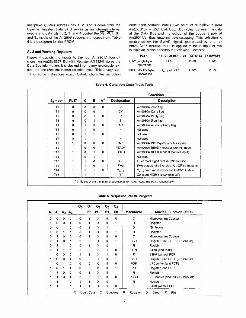
multiplexers, while address bits 1, 2, and 3 come from thePipeline Register. Data bit 0 serves as an interrupt internalenable and data bits 1, 2, 3, and 4 control the FE, PUP, 8 1 ,
and 8 0 inputs of the Am2909 sequencers, respectively. Table6 is the program for this PROM.
ALU and Working Registers
Figure 4 depicts the inputs to the four Am2901 A four-bitslices. An Am25LS377 Eight-Bit Register (U12324) stores theData Bus information. It is clocked in on every microcycle, except the one after the instruction fetch cycle. This is very useful for some instructions (e.g., Restart, where the instruction
code itself contains data.) Two pairs of multiplexers (fourAm25LS157 - U53, U54, U55, U56) select between the dataof the Data Bus and the output of the opposite pair ofAm2901 A's, thus enabling byte-swapping. This selection iscontrolled by the SWAP signal, generated by anotherAm25LS157 (9/U64). PL17 is applied to the 8 input of thismultiplexer, which performs the following functions:
PL17 1Y (en of HOP) 2Y (ROTATE) 3Y (SWAP)
LOW (single-byte PL18 PL19 LOWoperation)
HIGH (double-byte Cn+4 of LOP LOW PL19operation)
Table 5. Condition Code Truth Table.
Condition
Symbol PL37 C B A* Designation Description
TO 0 0 0 0 Z Am9080A Zero flag
T1 0 0 0 1 CY Am9080A Carry flag
T2 0 0 1 0 P Am9080A Parity flag
T3 0 0 1 1 S Am9080A Sign flag
T4 0 1 0 0 AC Am9080A Auxiliary Carry flag
T5 0 1 0 1 - not used
T6 0 1 1 0 - not used
T7 0 1 1 1 - not used
T8 1 0 0 0 INT Am9080A INT request (control input)
T9 1 0 0 1 READY Am9080A READY request (control input)
T10 1 0 1 0 HOLD Am9080A HOLD request (control input)
T11 1 0 1 1 - not used
T12 1 1 0 0 F3 F3 of most significant Am2901A slice
T13 1 1 0 1 F=O F=O outputs of all Am2901 A's OR'ed together
T14 1 1 1 0 Cn+4 Cn+4 from most significant Am2901A slice
T15 1 1 1 1 "1" Constant HIGH ("unconditional")
*c. B, and A are the internal equivalents of PL36, PL35, and PL34, respectively.
Table 6. Sequence PROM Program.
i I f i
°0 0 1 O2 0 3 0 4
A1 A2 A3 A4 FE PUP S1 SO Mnemonic Am2909 Function (Y = 1)
0 0 0 0 0 1 X 0 0 C Microprogram Counter
I0 0 0 1 0 1 X 0 1 R Register
0 0 1 0 0 1 X 1 1 D "D" Inputs
0 0 1 1 0 1 X 0 1 R Register
0 1 0 0 0 1 X 0 0 C Microprogram Counter
0 1 0 1 0 0 1 0 1 SBR Register (and PUSH ILPCounter)
0 1 1 0 0 1 X 0 1 R Register
0 1 1 1 0 0 0 1 0 RTN STKO (and POP)
1 0 0 0 1 1 X 1 0 F STKO (without POP)
1 0 0 1 0 0 1 0 1 SBR Register (and PUSH ILPCounter)
1 0 1 0 0 0 0 0 0 POP ILPCounter (and POP)
1 0 1 1 0 0 0 0 1 PR Register (and POP)
1 1 0 0 0 1 X 0 1 R Register
1 1 0 1 0 0 1 0 0 PUSH ILPCounter (and PUSH ILPCounter)
1 1 1 0 0 1 X 0 1 R Register
1 1 1 1 1 1 X 1 0 F STKO (without POP)
X = Don't Care C = Continue R = Register D = Direct F = File
7

By this arrangement, a single Control Bit (PL19) can be usedfor two different controls (SWAP, ROTATE), according towhether a single-byte or a double-byte operation is performed.The same device can also control the carry input (Cn ) of theHOP Am2901 A slices. In a double-byte operation, this Cnshould be the carry-out (Cn+4) of the LOP Am2901 A slices.However, in a single-byte operation, it should be determinedby a control bit of the microcode (PL18), which is identical tothe LOP Cn input. This is a simple example of microcodeformatting, as defined in Advanced Micro Devices' Micro-programming Handbook.
The four A register (source register) address lines of theAm2901 A's are fed from an Am25LS157 Multiplexer (U66). Itcan select as the source either bits Pl13 through Pl16 of themicroprogram or bits 0 through 2 of the Data Bus, latched inU1516 (Figure 3). In the latter case, the Most Significant Bit isalways LOW. Thus, bit PL22 ("A" Switch) controls whetherthe particular register is addressed by the microcode or themacrocode. The same is true for the B register (or destinationregister) address lines, this time using another Am25LS157Multiplexer (U65) and bit Pl33 ("B" Switch). Remember thatthe least significant address bit of both the source and destination register addresses is inverted in a single-byte operation. This is accomplished by an Am25LS153 Multiplexer(U63) and the "single/double" control bit PL17. However, in adouble-byte operation, the macroinstruction register pair address is used, and occupies only two bits in the destinationfield. In that case, the lSB of the B address is set to lOW(13/U63).
Two Am25LS257 Multiplexers (U76, Un) take care of the I/Oconnections necessary to execute all Rotate instructions. Onlyone of these two multiplexers is enabled at any time, according to Pl7, which is also 17 of the Am2901A instruction. Whenshifting, 17 =HIGH will cause an up-shift (rotate left inAm9080A terminology) and 17 =lOW a down-shift (rotateright). The rotate control signal, generated by 7/U64, selectsthe source of the shifted-in bit.
un participates in the rotate right instructions. The 1Y outputfeeds RAM3 of the HOP and the 2Y output feeds RAM3 of theLOP. The shifted-in bit will be either the shifted-out bit of thecorresponding pair of slices or the CY Flag. This is determined by whether an "around carry" (ROTATE=LOW) or a"through carry" (ROTATE=HIGH), respectively, is required.The 3Y output of un feeds 0 3 of the HOP and the 4Y outputfeeds 0 3 of the LOP. When ROTATE= LOW, the shifted-out0 0 bit of each pair will be shifted in, but whenROTATE= HIGH, the shifted-out 0 0 bit of the opposite pairwill be shifted in, thus performing a double-byte rotate. Thiscapability is one that is not contained in the Am9080A itself,but is a very useful feature in the emulation.
U76 performs a similar function in a rotate left instruction. Ascan be seen, the shifting-in of the Carry Flag in a "throughcarry" rotate instruction is implemented in hardware. Every rotate instruction requires that the Carry Flag be set accordingto the shifted-out bit. Although this could also be accomplished by using hardware, a software method was chosen fordemonstrational purposes. The bottom of Figure 5 shows thesystem outputs, the flag generation, and some control functions.
Instruction Decode
The nine I inputs of each Am2901 A slice are fed in parallel bybits PlO Ulrough Pl8 of the microprogram word. The Y outputs of the low order microprocessor pair are routed to two
8
Am2920 registers, U9394 (the Data register from the LOP, referred to in the microcode as "Dl"), whose outputs are tied tothe Data Bus, and U9596 (the Address register from the LOP,referred to as "Al"), whose outputs are tied to the eight leastsignificant bits of the Address Bus. Similarly, the Y outputs ofthe high order microprocessor pair are routed to two additional Am2920 registers, U10304 (the Data register from theHOP, called "DH" in the microcode) and U10506 (the Address register from the HOP, called "AH"). They are alsoconnected to an Am82S62 (U97), which generates the evenParity Flag.
The Output Enable's of both address registers (U10506 andU9596) are controlled by Pl27, which is actually the invertedHlDA. Thus, the Address Bus is placed in the highimpedance state when a hold is acknowledged. The Data Bushas three sources: U9394, U10304, and the Flag registersU101 and U102. One-half of an Am25LS139 Decoder/Demultiplexer (U131), using PL25 and Pl26 of the microinstructions as control inputs, assures that no more than oneoutput is enabled at any time. Since the 1YO output of thisdecoder is not connected, none of the register outputs areenabled when both PL25 and PL26 are LOW, and the DataBus is free for other communication purposes (e.g., mainmemory read). The other half of the same decoder (U131) directs the Am2901 A output to one of three sets of registers bycontrolling the Register Enable's: the two data registers(U9394, U10304) are controlled by the OCl 1 line, the twoaddress registers (U9596, U10506) by the OCl 2 line, andthe INTE register (U111) by the OCl 3 line.
Status Bits
In order to shorten the execution time by interleaving severaldifferent operations, it is necessary to delay the updating ofthe address registers when the READY input is LOW. This isrequired until the I/O or main memory completes its read orwrite cycle (and sets READY to HIGH). If the 2Y2 output ofU131 is selected (lOW) by PL23 and PL24, and READY (T9)is HIGH, then 13/Ul13 will go HIGH and the OCl 2 line lOW,thus allowing the address registers to latch their input. However, if at the same time READY is lOW there is an I/O ormemory reference operation (PL28 or PL29 or Pl30 or PL31is LOW), then 6/U73 will be lOW. This will bring both 10/Ul13 and OCL 2 HIGH, thus blocking the data coming in tothe address registers.
The INTE (Interrupt Enable) control output of the Am9080A isa single-bit, software-controlled flag. An Am2920 (U111) isused to store its state. The flag is generated by usingsoftware to manipulate the MSB's of the HOP Am2901 Aslices, using the most significant F3 output. Pl23 and PL24,through U131 and the OCL 3 control line, determine whetheror not to update this status. The INTE output is also used inthe interrupt recognition circuit (9/U73, Fig. 3), as describedabove.
The five Am9080A flags are stored in two Am2918 registers;U102 stores the CY Flag and U101 the others. The Y Outputsof these registers are connected to the Data Bus and are controlled by DB3, which is generated by U131. This enablesPUSH PSW, where the contents of the A register are writteninto the stack. The input of U101 is fed from an Am25LS157MUltiplexer (U91). The B inputs of this multiplexer come froman additional Am25LS157 (Ul15). Usually, Ul15 will passwhatever data is appearing on the Q outputs of U101 to the Binputs of U91. Bit PL20, when HIGH, will pass this data backto UHU, thus storing ttleprevious oontentsof UHH. This isthe case when the flags are not affected. The 1A input of U91

(the Z flag) comes from the F=0 outputs of the Am2901 Aslices, all of which are tied together and pUlled up to Vee by a1KO resistor. The 2A input of U91 (the P flag) comes from theAm82S62 Parity Generator (U97). The 3A input of U91 (the Sflag) comes from the F3 output of U34. The 4A input of U91(the AC flag) comes from the Cn+4 output of U33, through anAND gate. Thus, when PL20 is LOW, the new flags will belatched in U1 01. This is the case when the flags are affected.
As mentioned earlier, the case for the CY flag is somewhatdifferent. PL3, PL4, and PL5 are the 13, 14, and 15 instructionbits of the Am2901A slices, respectively. The logic operationsare decoded from these bits to cause 1/U113 to go LOW.This resets, using two AND gates, both the CY flag comingfrom the Cn+4 output of U34 (which is applied to the 1COinput of an Am25LS153 Multiplexer - U92) and the AC flag(as mentioned before). The two subtract operations are alsodecoded and they control the A control input of U92, selectingthe complement of the carry as the CY flag, through the 1C1input. If PL21 is HIGH, the previous carry is directed back toU102 through U125.
Both U125 and U115 (two Am25LS157 multiplexers) effectthe POP PSW instruction. Here, the flags are read from themain memory and are stored in the flag registers U101 andU102. The NAND function of the Am2901A's (when 1345 =
101) is used for this purpose and this purpose only. This function is decoded and applied to the S input of both multiplexers(1/U115 and 1/U125), thus moving the flags latched in thedata register U12324 (Figure 3) to their proper registers(U101, U102). This is an example of microprogram formatting,since the 1345 bits are used for two different purposes.
The a outputs of the Flag Registers are also applied to theappropriate inputs of the condition code multiplexers U8474and U8475 (Figure 3 and Table 5).
An Am25LS374 register (U121) is used to latch both the incoming INT, READY, and HOLD control signals and theCn+4 , F=O, and F3 micro-flags, and then to apply them to thecondition code multiplexers.
Timing Considerations
Two worst case speed paths are calculated in Table 7: TheControl Path and the Data Path. In each case, the maximumand typical values are shown using Am25LS commercial parts(Vcc = 5V, TA = 25°C). Two additional columns areshown: maximum and typical values if "S" type parts areused, when applicable. The calculation point is from theLOW-to-HIGH transition of the clock pulse until the nextLOW-to-HIGH transition of the clock (in ns).
Table 7. Speed Path Calculations.
Designation Device Type Path
Control Path
Am25LS
Typ. Max.
"S"
Typ. Max. Remarks
U5161, U121 Am25LS374 CP-+Y 22 37 11.5 17 Note 1
U62 74LS04 In -+ Out 10 15 not needed
U8475 Am2922 OE -+Y 10 17 10 17
U14 Am29751 A-+O 32 50 32 i 50
U21 Am2909 ISOS1 -+ Cn+4 50 I 50 50 ! 50I
U22 Am2909 Cn -+ Cn+4 18 ! 18 18 18
Microprogram Memory Am29773 A-+D 35 I 50 35 50
Pipeline Register Am25LS374 I Set-up 20 i 20 5 5
I Total 197 I 257 161.5 207i
Data Path
Pipeline Register Am25LS374 CP -+Y 22 37 11.5 17
U65, U66 Am25LS157 S-+Y 15 23 12 18 Note 2
U62 74LS04 In -+ Out 10 15 3 5
U63 Am25LS153 C-+Y 10 16 not needed
U43 Am2901 A A, B -+ Cn+4 75 75 75 75
U44 Am2901 A Cn -+ Cn+4 20 20 20 20
U64 Am25LS157 A-+Y 8 12 4.5 6.5
U33 Am2901 A Cn -+ Cn+4 20 20 20 20
U34 Am2901 A Cn -+ F=O 50 50 50 I 50
U91 Am25LS157 A-+Y 8 12 4.5 6.5
U101 Am2918 Set-up 5 5 5 5
Total 242 285 205.5 223
Notes: 1. This path was calculated using an Am74S175 to drive the OE's of U8474 and U8475 from its Q and Qoutputs simultaneously.2. This path was calculated using an Am74S151 to mUltiplex the LSB of the A, B addresses.
9
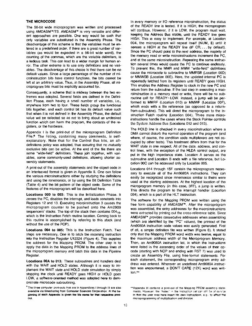
THE MICROCODE
The 56-bit wide microprogram was written and processedusing AMDASM™/TS. AMDASM™ is very versatile and different approaches are possible. One way would be such thatonly variables are substituted in the Assembly Phase. Thedisadvantage of this scheme is that the variables must be entered in a predefined order. If there are a great number of variables (as would be expected in a 56-bit wide word), thecounting of the commas, which are the variable delimiters, isa tedious task. This can lead to a wider margin for human error. The other extreme is to use only definitions and no variables. The disadvantage of this choice is that there can be nodefault values. Since a large percentage of the number of microinstruction bits have control fun~tions, the bits cannot beleft at an arbitrary value. Thus, in the Assembly Phase, all microprogram bits must be explicitly accounted for.
Consequently, a scheme that is midway between the two extremes was adopted. Several fields are defined in the Definition Phase, each having a small number of variables, I.e.,anywhere from two to four. These fields group the functionalbits together, and each control bit has its default value suchthat when it is not defined in the Assembly Phase, the defaultvalue will be selected so as not to bring about an undesiredfunction which can harm the program, the contents of the registers, or the hardware.
Appendix I is the print-out of the microprogram DefinitionFile.* The listing, containing many comments, is selfexplanatory. Note that for the Control Bus bits, an alldefinitions policy was adopted, thus assuring that no mutuallyexclusive bits can be active. At the end of the file there aresome "wide-field" definitions. These join together, with variables, some commonly-used definitions, allowing shorter assembly statements.
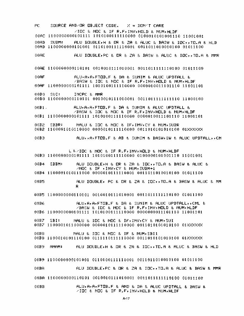
A print-out of the assembly statements and the object code inan interleaved format is given in Appendix II. One can followthe various microinstructions either by studying the definitionsand using the mnemonics, or by using the Bit Definition Table(Table 4) and the bit pattern of the object code. Some of thefeatures of the microprogram will be described here.
Locations 000 to 003: This is the Initialization Phase. Itzeroes the PC, disables the interrupt, and loads constants intoRegisters 12 and 13. Executing microinstruction 3 causes themicroprogram counter to be pushed onto the Am2909sequencers' stacks. The top of the stack then contains 00416,
which is the Instruction Fetch routine location. Coming back tothis routine is accomplished by referring to this stack (andwithout the use of the POP).
Locations 004 to 005: This is the Instruction Fetch. Twosteps are necessary. One is to latch the incoming instructioninto the Instruction Register U12324 (Figure 4). This suppliesthe address for the Mapping PROM. The other step is toapply the data in the Mapping PROM to the address lines ofthe microprogram memory and latch this data in the PipelineRegister.
Locations OOA to 013: These subroutines and handlers dealwith the WAIT and HOLD states. Although it is easy to implement the WAIT state and HOLD state simulation by simplystopping the clock until READY goes HIGH or HOLD goesLOW, a software-oriented method was adopted here to demonstrate microcode subroutining.*The three computer print-outs that are in Appendices I through III are also
available via timesharing from Computer Sciences Corporation. At the begMlning of each Appendix is given the file~ tor ....r~ pOOt
out.
10
In every memory or I/O reference microinstruction, the statusof the READY line is tested. If it is HIGH, the microprogramwi!! continue. However, if it is LOW, the program must wait,keeping the Address Bus stable, until the READY line goesHIGH. This is easy to implement. For example, at Location004, the microprogram will repeat itself (NUM, $) until itsenses a HIGH at the READY line (IF CR, ... by defaUlt).Since the PC should point to the next address, the majority ofthe memory read or write microinstructions increment the PC,and at the same microinstruction. Repeating the same instruction several times would cause the PC to continue endlessly.To prevent this, the MMR and MMW "wide-field" definitionscause the microcode to subroutine to MMRSB (Location OOD)or MMWSB (Location OOE). Here, the updated internal PC isrepeatedly fetched from its registers until READY goes HIGH.This enables the Address Register to clock in the new PC andreturn from the subroutine. If the last step in executing a macroinstruction is a memory read or write, there will be no subroutine call for READY=LOW. Instead, a jump will be performed to MMRF (Location 010) or MMWF (Location OOF),which ends with a file reference (as opposed to a returnfrom-subroutine). This will direct the microprogram to the Instruction Fetch routine (Location 004). Three more microinstructions handle the cases where the Stack Pointer controlsthe System Address Bus (Locations 012 and 013).
The HOLD line is checked in every microinstruction where aDMA cannot disturb the normal operation of the program (andwhere, of course, the condition code multiplexers are not occupied by other tests). This treatment differs from that for theWAIT state in one respect. All of the data, address, and control lines, with the exception of the HLDA control output, areput in the high impedance state. Location A serves as thesubroutine and Location B ends with a file reference, but Location OOC can be accessed only by Location 005.
Locations 014 through 15F contain the microprogram necessary to execute all of the Am9080A instructions. They caneasily oe recognized since mnemonics similar to theirs wereused at the starting addresses. At the highest location of themicroprogram memory (in this case, 3FF), a jump is written.This directs the program to the interrupt handler (Location084), which is a part of the HLT instruction.
The software for the Mapping PROM was written using thefree form capability of AMDASM™. After the microprogramwas assembled, the entry addresses for the macroinstructionswere extracted by printing out the cross-reference table. SinceAMDASM™ provides consecutive addresses when assembling(which are identified by the "PC" values), the printout of theAm9080A instruction code values was easily generated. Firstof all, a simple definition file was written (Figure 6). It statedonly that the Mapping PROM word width was twelve, equal tothe maximum address width of the Microprogram Memory.Then, an Am9080A instruction list, in which the instructionswere listed in the ascending order of the values of their opcode (starting with NOP and ending with RST 7) was used tocreate an Assembly File, using free-format statements. Foreach statement, the corresponding microprogram entry address was entered. Wherever an undefined Am9080A instruction was encountered, a DON'T CARE (12X) word was written.**
--AppendiX III contains a print-out of the Mapping PROM assembly statements. However. the "holes" in the instruction set can still be of servicein ttlat tile user may here· insert h+s OWl"\' instnrcttons, e. g.. to effect ttlemicroprogramming of multiplication and division.

TITLE 8080EMULATOR MAPPING PROM DEFINITIONS!.•.IDRII 12ENII.....
Figure 6. Mapping PROM Definition File.
Since all register reference instructions use the same microcode, the AMDASM™ DUP statement was used to shortenthe file. After the assembly is run, the output (Appendix III)lists the Am9080A instruction code as address and the appropriate microprogram entry point as data. This data can befurther processed by AMPROM™ to punch a paper tape toprogram the Am29761 PROM's.
SUMMARY
The particular design used in this application note is by nomeans a unique method to emulate the Am9080A/Am8228chip set. It is intended to serve as an example of such anemulation and, in doing so, to bring about some reduction inexecution times. Variations are possible, both to alter thenumber of devices used and to reduce the number of cyclesnecessary to execute the instructions. Also, additional performance improvement can be achieved by adding architecturalenhancements, such as overlap fetch of the next machine instruction.
Device
Am2901AAm2909Am2918Am2920Am2922Am29751Am29761Am29773Am25LS139Am25LS153Am25LS157Am25LS257Am25LS374Am25LS377Am82S6274S0874LS0274LS0474LS21
PARTS LIST
Description
Four-Bit Bipolar Microprocessor SliceMicroprogram SequencerFour-Bit Register with Standard and Three-State OutputsEight-Bit Register with Three-State Outputs and Clear and EnableEight-Input MUltiplexer with Control Storage32 x 8 PROM with Three-State Outputs256 x 4 PROM with Three-State Outputs512 x 8 PROM with Three-State OutputsDual One-of-Four Decoder/DemultiplexerDual Four-Input MultiplexerQuad Two-Input Multiplexer, Non-InvertingQuad Two-Input Multiplexer with Three-State Outputs, Non-InvertingOctal D-Register with Three-State OutputsOctal D-Register with Common EnableSchottky Nine-Input Parity Checker/GeneratorQuad Two-Input AND GateQuad Two-Input NOR GateHex InverterDual Four-Input AND Gate
Qty.
4325213712
1028212121
Total 59

APPENDIX IMicrocode Definition Fileesc File Name: AMDEF
A-1
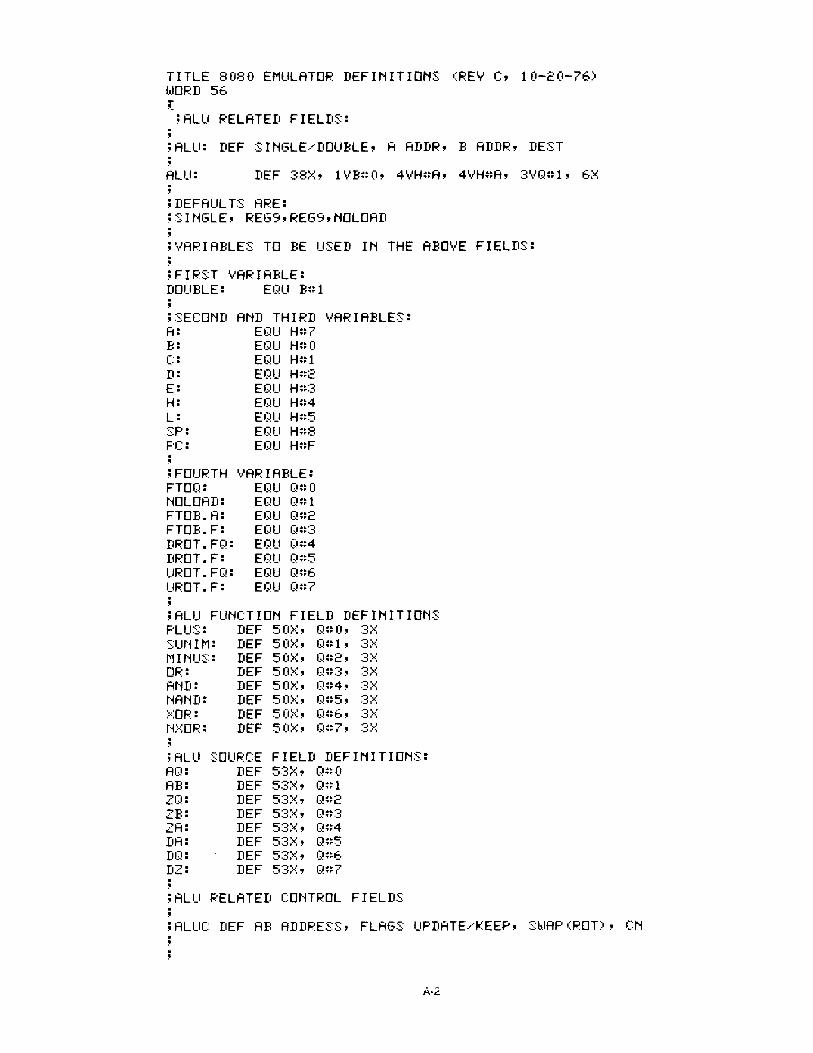
TITLE 8080 EMULATOR DEFINITIONS (REV C, 10-20-76)I.I.IORD 5E.r
;ALU RELATED FIELDS:
;ALU: DEF SINGLE/DOUBLE, A ADDR, B ADDR, DEST
DEFAUL TS: ARE:SINGLE, REG9,REG9,NOLOAD
VARIABLES TO BE USED IN THE ABOVE FIELDS:
FIRST VARIABLE:DOUBLE: EQU Bel
; :S:ECONDA:E' •,.1-· •_..D:E:H:L:SP:PC:
;FOURTHFTOG!:t·mLOAD:FTOB.A:FTOB.F:DROT.FQ:DROT.F:UFmT. FQ:UROT.F:
AND THIRIIEOU H~~7
EOU H~~O
EG!U H~~l
EOU H~~2
EOU H~~:3
EOU H~~4
EC!U H~~5
EC!U H~~8
EOU H~~F
VARIABLE:EI~U Q~~O
EOU O~~ 1EG!U G!~~2
EOU 0~~:3
EG!U Q~~4
EOU Q~~5
EG!U Q~~6
EI~U C!~~7
VARIABLES:
G!~~2 , 3><G~~~:3 !t 3>::Q~~4, :3:>::t;!~~5 , :3:"':G~~=6 , 3>0:G~~~7, :3:=-::
;ALU FUNCTION FIELD DEFINITIONSPLUS: DEF 50X, OeO, 3XSUNIM: DEF 50X, Qel, 3Xt'1INUS:: DEF 50X,OR: DEF 50><,At·m: DEF 50>::,NAND: DEF 50>0:,::-::OF.~: DEF 50>0:,N::-::OR: DEF 5 moe;,
;ALU :S:OURCE FIELD DEF IN I TIONS::AO: DEF 53>:: , o::~o
AB: DEF 5:3>:: , emlZO: DEF 5:3>:: , G!~~2
ZB: DEF 53>0: , 0~~:3
ZA: DEF 5:3::< , G!~~4
DA: DEF 5:3:X: , O~~5
DO: DEF 5:~:>:: , G!~~6
DZ: DEF 5:3:>:: , 1~~~7
;ALU RELATED CONTROL FIELDS
;ALUC DEF AB ADDRESS, FLAGS UPDATE/KEEP, SWAP (ROT) , eN

ALUC: DEF :34:x:, 2VB~~11, lVB~~O, lVB~~l, 18:X:
;VARIABLES TO BE USEDUPDTCY: EQU B~Ol
UPDTFL: EQU B~10
UPDTALL: EQU'B~OO
SWAP: EQU B~l
~NL: EQU B=O
NOT E: WHEN SINGLE IS DEFINED IN ALU~S FIRST VARIABLE~SWAP' WILL CAUSE ROTATION WITH CY SHIFTED IN;AND NOSWAP WILL CAUSE WRAP-AROUND ROTATION!
.A AND B ADDRESS SWITCH:BAS:J.,.I: DEF 22X, 1VB~~ 0, 1O:X:, 1VB~~ 0, 22:X:~W: EQU B~l
1.···-0 CUNTROLS:
IOC: DEF DATA IN LATCH, DATA-BUS, 2901 OUTPUT LATCH
IOC: DEF lVB~l, 28X, 2VB=00, 2VB=OO, 2:3X
;VARIABLE FO THE FIRST FIELD.IN: EG!U B~~O
;VARIABLES FOR THE SECOND FIELD:DL: EQU B=OlDH: EQU B~~10
FLAGS: EQU B=ll
;VARIABLES FOR THE THIRD FIELD:TO.D: EQU B=OlTO.A: EQU B=10TO.INTE: EQU B~ll
;CONTROL-BUS FIELD DEFINITIONS
tiOC: DEF 2:3X, B~~ 111110, 27 'xI ••
MEMI,J: DEF 2:3><: , B~~ 111100, 27><:MEMR: DEF 2:3X, B~~ 111010, 27:=<:IOI,J: DEF 23X, B~~110110, 27:X:lOR: DEF 2:3X, B~~ 10111 0, 27:X:INTA: DEF 2:3:X: , B~~ 011110, 27:X:HLDA: DEF 2:3:X: , B~~ 111111, .-...... y..
C(."I
;TEST SELECT, POLARITY AND NEXT INSTRUCTION FIELDS:
;IF DEF NEXT INSTR., POL, TESTIF: DEF 14:X:, :3VQ~~O, lVB~~l, 4VH~~F,:34>c;
;NEXT INSTRUCTION VARIABLES:
; (FALSE. TRUE)C. R: EQU Q~~O
D. R: EQU Q~~l
C.SBR: EQU Q=2R. RTN: EQU O~~:3
F.SBR: EQU Q~4
PDP. PR : EDt! Q~~5
A-3

F.~. PU:S:H:F.~ • F:
EG!U O~~tS
EG!U O~~7
;C=CONTINUE; R=REGISTER; D=DIRECT(MAP);;SBR=SUBROUTINE REGISTER; RTN=RETURN FROM SUBROUTINE;;F=FILE REFERENCE; PUSH=PUSH AND CONTINUE;POP=POP AND CONTINUE; PR=POP AND BRANCH REGISTER
EOU B~~O
; TES:Tz:Cl:p:s::AC:HiT:READ..,.':HOLD:F·"j·
"-' -FO:CN.4:
VARIABLES:EOU H~~O
EOU H~~l
EOU H~~2
EQU H~~3
EOU H~~4
EOU H~~8
EOU H~~9
EI;!U H~~A
EQU H~~C
EG'U H~~D
E@J H~~E
;THE NUMERICAL FIELD IS 12 BIT WIDE. THE 8 LS BITS CAN BE;USED FOR DIRECT DATA BY LETTING THE FIRST VARIABLE TO 'DBUS'
; NUM DEF DB, NUMBER IN HEXA.tKIM: DEF 1X, 1VB~~1, 12V~-;;H~~000, 42X
;VARIABLE TO BE USED:DBUS: EOU B=O;; I.~I I DEMMR:I"'lt%.1 :HLD:INCPC:FMMR:FMMh.l:t-iALU:E~m
E~m...
FIELD DEFINITIONS:DEF 1:X:, B~~ 1, 12rl~~ 13::'~, G!~~2, B~~ 0, H~~9,
DEF 1:X:, B~~ 1, 12rJ~~14%, Q~~2, B~~ 0, H~~9,
DEF 1:X:, B~~ 1, 12D~~1 O~·~, O~~2, B~~ 1, H~~A,
DEF B~~ 1, 21:X:, B~~ 0, 6:X:, B~~ 001 0011 011 ,DEF B~~ 11, 12V~-;;, H~~ 0976, H~~ OC551, 6XDEF E:~~ 11, 12V::'~, H~~0979, H~~ OC551, 6:X:
DEF 22:X:, B~~O, 1 O:X:, B~~O, H~~D, B~~O, H~~AA,
A-4
lX, O~~72, 27X1X, G!~=74, 27X1X, G!~~7E" 27XH~~FF, O~~:304

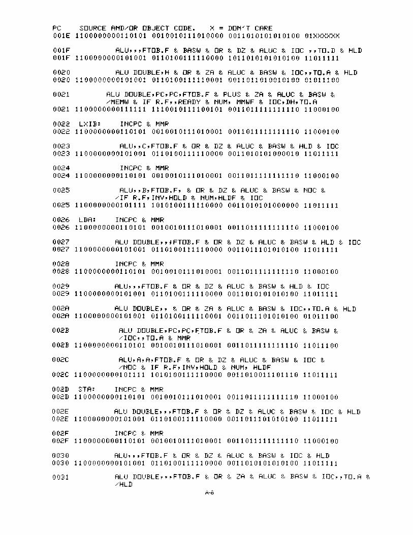
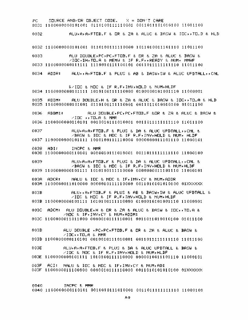
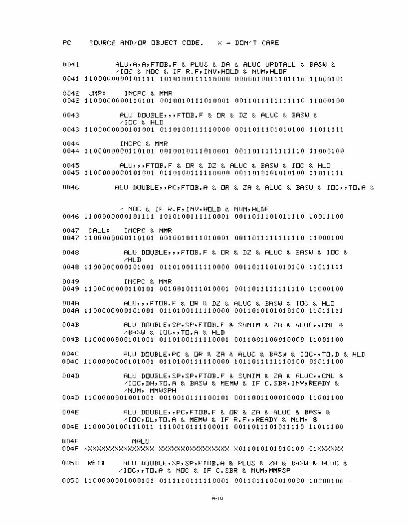
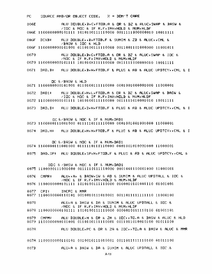
APPENDIX IIMicrocode Source Code and Object Code Output
In Interleaved Format CSC File Name: AM800
Note: A listing of the Source Code (Assembly File) only may be obtained using CSC FileName AMASSY.
A-5

EMULATOR ASSEMBLY (MARCH 1977)07/06/77
PC SOURCE AND/OR OBJECT CODE. x = DON~T CARE
0000 ; INITIALIZATION:
0000 RESET: ALU DOUBLE, PC,PC,FTOB.F & AND & ZA & ALUC & BASW &/IOC"TO.INTE & IF,INV, & NUM DBUS,H=38 & NOC
0000 1000000011100000 0011110111110001 1011011111111110 11100100
0001 ~LU"H=D,FTOB.F & DR & DZ & ALUC & BASW & IOC &/NOC & IF,INV & NUM
0001 1100000000000000 0011110111110000 0011010101011010 11011111
0002 ALU"H~~C,FTOB.F & AND & ZA & ALUC & BASW & IOC &/NOC & IF,INV & NUM
0002 1100000000000000 0011110111110000 0011010101011000 11100100
0003 ALU",FTOB.F & AND & ZA & ALUC & BASW & IOC"TO.A &/NOC & IF R.PUSH & NUM
0003 1100000000000011 0111110111110001 0011010101010100 11100100
0004 FETCH: ALU DOUBLE,PC,PC,FTOB.F & DR & ZA & ALUC & BASW &/IOC IN"TO.A & MEMR & IF ,INV,READY & NUM, $
0004 0100000000010000 0010010111010001 0011011111111110 11011100
0005 INCPC & IF D.R, ,HOLD & NUM,HLDD & NOC0005 1100000000110000 1110100111110001 0011011111111110 11000100
0000
0000 ;HOLD AND MEMORY REFERENCE SUBROUTINES AND HANDLERS:
0000
0000 ORG 10
OOOA HLDSB: NALU & IOC & HLDA & IF R.RTN, INV, HOLD & NUM, $OOOA 1100000000101001 1010100111111000 0011010101010100 01XXXXXX
OOOB HLDF: NALU & IOC & HLDA & IF R.F,INV,HOLD & NUM, $OOOB 1100000000101111 1010100111111000 0011010101010100 01XXXXXX
OOOC HLDD: NALU & IOC & HLDA & IF D.R"HOLD & NUM, $OOOC 1100000000110000 1110100111111000 0011010101010100 01XXXXXX
OOOD MMRSB: ALU DOUBLE,PC,PC,FTOB.F & DR & ZA & IOC"TO.A &/ALUC & MEMR & IF R.RTN, ,READY & NUM , $ & BASW
OOOD 1100000000110101 1110010111010001 0011011111111110 11011100
OOOE MMWSB:
MW
ALU DOUBLE,PC,PC,FTOB.F & DR & ZA & ALUC &/IOC, DH, TO.A & NUM , $ & IF R.RTN"READY & BASW & ME
OOOE 1100000000111001 1110010111100101 0011011111111110 11011100
OOOF MMWF: ALU DOUBLE,PC,PC,FTOB.F & DR & ZA & ALUC & BASW &/MEMW & IF R.F"READY & IOC, DH,TO.A & NUM, $
OOOF 1100000000111111 1110010111100101 0011011111111110 11011100
0010 MMRF: ALU DOUBLE~PC~PC~FTOB.F & OR & ZA & ALUC & BASW & MEMR &
A-6
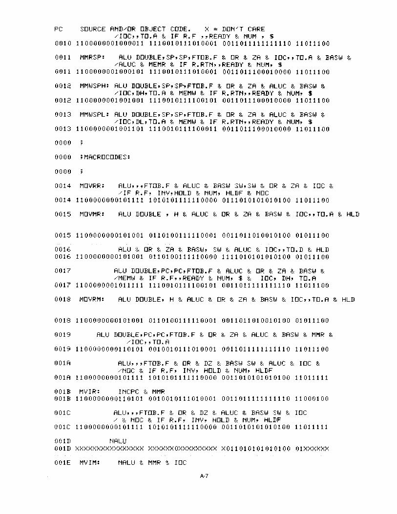
PC SOURCE AND/OR OBJECT CODE. X = DON/T CARE/IOC"rO.A & IF R.F "READY & NUM , $
0010 1100000001000011 1110010111010001 0011011111111110 11011100
0011 MMRSP: ALU DOUBLE,SP,SP,FTOB.F & DR & ZA & IOC"TO.A & BASW &/ALUC & MEMR & IF R.RTN, ,READY & NUM, $
0011 1100000001000101 1110010111010001 0011011100010000 11011100
0012 MMWSPH: ALU DOUBLE,SP,SP,FTOB.F & DR & ZA & ALUC & BASW &/IOC,DH,TO.A & MEMW & IF R.RTN"READY & NUM, $
0012 1100000001001001 1110010111100101 0011011100010000 11011100
0013 MMWSPL: ALU DOU~LE,SP,SP,FTOB.F & DR & ZA & ALUC & BASW &/IOC,DL,TO.A & MEMW & IF R.RTN"READY & NUM, $
0013 1100000001001101 1110010111100011 0011011100010000 11011100
0000
0000 ;MACROCODES:
0000
0014 MDvRR: ALU",FTDB.F & ALUC & BASW SW,SW & DR & ZA & IDC &/IF R.F, INV,HOLD & NUM, HLDF & NOC
0014 1100000000101111 1010101111110000 0111010101010100 11011100
0015 MOVMR: ALU DOUBLE, H & ALUC & DR & ZA & BASW & IOC"TO.A & HLD
0015 1100000000101001 0110100111110001 0011011010010100 01011100
0016 ALU & DR & ZA & BASW, SW & ALUC & IOC"TO.D & HLD0016 1100000000101001 0110100111110000 1111010101010100 01011100
0017 ALU DOUBLE,PC,PC,FTOB.F & ALUC & DR & ZA & BASW &/MEMW & IF R.F"READY & NUM, $ & IOC, DH, TO.A
0017 1100000001011111 1110010111100101 0011011111111110 11011100
0018 MOVRM: ALU DOUBLE, H & ALUC & DR & ZA & BASW & IOC"TO.A & HLD
0018 1100000000101001 0110100111110001 0011011010010100 01011100
0019 ALU DOUBLE,PC,PC,FTOB.F & DR & ZA & ALUC & BASW & MMR &/IOC"TO.A
0019 1100000000110101 0010010111010001 0011011111111110 11011100
001A ALU",FTOB.F & DR & DZ & BASW SW & ALUC & IOC &/NOC & IF R.F, INV, HOLD & NUM, HLDF
001A 1100000000101111 1010101111110000 0011010101010100 11011111
001B MVIR: INCPC & MMR001B 1100000000110101 0010010111010001 0011011111111110 11000100
001C ALU",FTOB.F & DR & DZ & ALUC & BASW SW & IOC/ & NOC & IF R.F, INV, HOLD & NUM, HLDF
001C 1100000000101111 1010101111110000 0011010101010100 11011111
00lD NALU001D XXXXXXXXXXXXXXXX XXXXXXOXXXXXXXXX X011010101010100 01XXXXXX
001E MVIM: NALU & MMR & IoC
A-7
PC SOURCE AND/OR OBJECT CODE. X = DoN'"T CARE001E 1100000000110101 0010010111010000 0011010101010100 01XXXXXX
001F ALU",FToB.F & BASW & OR & DZ & ALUC & IDC "TD.D & HLD001F 1100000000101001 0110100111110000 1011010101010100 11011111
0020 ALU DDUBLE,H & OR & ZA & ALUC & BASW & IDC"TO.A & HLD0020 1100000000101001 0110100111110001 0011011010010100 01011100
0021 ALU DoUBLE,PC,PC,FToB.F & PLUS & ZA & ALUC & BASW &/MEMW & IF R.F"READY & NUM, MMWF & IoC,DH,TD.A
0021 1100000000111111 1110010111100101 0011011111111110 11000100
0022 LXIB: INCPC & MMR0022 1100000000110101 0010010111010001 0011011111111110 11000100
0023 ALU"C,FToB.F & OR & DZ & ALUC & BASW & HLD & IoC0023 1100000000101001 0110100111110000 0011010101000010 11011111
0024 INCPC & MMR0024 1100000000110101 0010010111010001 0011011111111110 11000100
0025 ALU"B,FToB.F, & OR & DZ & ALUC & BASW & NoC &/IF R.F,INV,HoLD & NUM,HLDF & IDC
0025 1100000000101111 1010100111110000 0011010101000000 11011111
0026 LDA: INCPC & MMR0026 1100000000110101 0010010111010001 0011011111111110 11000100
0027 ALU DDUBLE"JFTDB.F & OR & DZ & ALUC & BASW & HLD & IDC0027 1100000000101001 0110100111110000 0011011101010100 11011111
0028 INCPC & MMR0028 1100000000110101 0010010111010001 0011011111111110 11000100
0029 ALU",FToB.F & OR & DZ & ALUC & BASW & HLD & IDC0029 1100000000101001 0110100111110000 0011010101010100 11011111
002A ALU DOUBLE" & OR & ZA & ALUC & BASW & IDC"TD.A & HLD002A 1100000000101001 0110100111110001 0011011101010100 01011100
002B ALU DDUBLE,PC,PC,~TDB.F & OR & ZA & ALUC & BASW &/IDC"TD.A & MMR
002B 1100000000110101 0010010111010001 0011011111111110 11011100
002C ALU,A,A,FTDB.F & OR & DZ & ALUC & BASW & IDC &/NoC & IF R.F,INV,HDLD & NUM, HLDF
002C 1100000000101111 1010100111110000 0011010011101110 11011111
002D STA: INCPC & MMR002D 1100000000110101 0010010111010001 0011011111111110 11000100
002E ALU DDUBLE",FTDB.F & OR & DZ & ALUC & BASW & IDC & HLD002E 1100000000101001 0110100111110000 0011011101010100 11011111
002F INCPC & MMR002F 1100000000110101 0010010111010001 0011011111111110 11000100
0030 ALU",FTDB.F & OR & DZ & ALUC & BASW & IDC & HLD0030 1100000000101001 0110100111110000 0011010101010100 11011111
0031 ALU DOUBLE",FTOB.F & OR & ZA & ALue & BASW & IOC"TO.A &/HLD
PC SOURCE AND/OR OBJECT CODE. X = DON~T CARE0031 1100000000101001 0110100111110001 0011011101010100 11011100
0032
0032 1100000000101001 0110100111110000 1011010011101110 11011100
0033 ALU DOUBLE,PC,PC,FTOB.F & DR & ZA & ALUC & BASW &/IOC,DH,TO.A & MEMW & IF R.F"READY & NUM, MMWF
0033 1100000000111111 1110010111100101 0011011111111110 11011100
00:34 ADDR: ALU"A,FTOB.F & PLUS & AB & BASW,SW & ALUC UPDTALL"CNL
&/IOC & NOC & IF R.F,INV,HOLD & NUM,HLDF0034 1100000000101111 1010100111110000 0100000101001110 11000001
0035 ADDM: ALU DOUBLE,H & DR & ZA & ALUC & BASW & IOC"TO.A & HLD0035 1100000000101001 0110100111110001 0011011010010100 01011100
0036 ADDMl: ALU DOUBLE,PC,PC,FTOB.F &OR & ZA & ALUC & BASW &/IDC "TD.A & MMR
0036 1100000000110101 0010010111010001 0011011111111110 11011100
0037 ALU,A,A,FTOB.F & PLUS & DA & ALUC UPDTALL"CNL &/BASW & IOC & NOC & IF R.F,INV,HOLD & NUM, HLDF
0037 1100000000101111 1010100111110000 0000000011101110 11000101
0038 ADI: INCPC &: MMR0038 110UOOOOOOII0101 OUI00I0111010aOI 0011al111111111U llUOUlao
0039 ALU,A,A,FTOB.F & PLUS & DA & ALUC UPDTALL"CNL &/BASW & IOC & NOC & IF R.F,INV,HOLD & NUM,HLDF
0039 1100000000101111 1010100111110000 0000000011101110 11000101
003A ADCR: NALU & IOC & NOC & IF,INV,CY & NUM,ADDR003A 1100000011010000 0000010111110000 0011010101010100 01XXXXXX
003B ALU"A,FTOB.F & PLUS & AB & BASW,SW & ALUC UPDTALL &/IOC & NOC & IF R.F,INV,HOLD & NUM,HLDF
003B 1100000000101111 1010100111110000 0100010101001110 11000001
003C ADCM: ALU DOUBLE,H & OR & ZA & ALUC & BASW & IOC"TO.A &/NOC & IF,INV,CY & NUM,ADDMI
003C 1100000011011000 0000010111110001 0011011010010100 01011100
003D ALU DOUBLE ,PC,PC,FTOB.F & OR & ZA & ALUC & BASW &.····IOC, ,TO. A t: MMR
003D 1100000000110101 0010010111010001 0011011111111110 11011100
003E ALU,A,A,FTOB.F & PLUS & DA & ALUC UPDTALL & BASW &/IOC & NOC & IF R.F,INV,HOLD & NUM,HLDF
003E 1100000000101111 1010100111110000 0000010011101110 11000101
003F ACI: NALU & IOC & NOC & IF,INV,CY & NUM,ADI003F 1100000011100000 0000010111110000 0011010101010100 01XXXXXX
004(1 INCPC t.: MMP.0040 1100000000110101 0010010111010001 0011011111111110 11000100
A-9
PC SOURCE AND/OR OBJECT CODE. x = DON'T CARE
0041 ALU~A~A~FToB.F & PLUS & DA & ALUC UPDTALL & BASW &/IoC & NoC & IF R.F~INV~HoLD & NUM~HLDF
0041 1100000000101111 1010100111110000 0000010011101110 11000101
0042 JMP: INCPC & MMR0042 1100000000110101 0010010111010001 0011011111111110 11000100
0043 ALU DoUBLE~~~FToB.F & OR & D2 & ALUC & BASW &/IoC & HLD
0043 1100000000101001 0110100111110000 0011011101010100 11011111
0044 INCPC & MMR0044 1100000000110101 0010010111010001 0011011111111110 11000100
0045 ALU~~~FToB.F & OR & D2 & ALUC & BASW & IoC & HLD0045 1100000000101001 0110100111110000 0011010101010100 11011111
0046 ALU DOUBLE"PC,FTDB.A & DR & 2A & ALUC & BASW & IDC"TD.A &
/ NoC & IF R.F~INV~HoLD & NUM~HLDF
0046 1100000000101111 1010100111110001 0011011101011110 10011100
0047 CALL: INCPC & MMR0047 1100000000110101 0010010111010001 0011011111111110 11000100
0048 ALU DoUBLE~~~FToB.F & OR & D2 & ALUC & BASW & IoC &/HLD
0048 1100000000101001 0110100111110000 0011011101010100 11011111
0049 INCPC & MMR0049 1100000000110101 0010010111010001 0011011111111110 11000100
004A ALU",FToB.F & OR & DZ & ALUC & BASW & IoC & HLD004A 1100000000101001 0110100111110000 0011010101010100 11011111
004B ALU DoUBLE,SP,SP,FToB.F & SUNIM & ZA & ALUC"CNL &/BASW & IoC~~To.A & HLD
004B 1100000000101001 0110100111110001 0011~01100010000 11001100
004C ALU DoUBLE~PC & OR & ZA & ALUC & BASW & IoC~~To.D & HLD004C 1100000000101001 0110100111110000 1011011111110100 01011100
004D ALU DoUBLE~SP~SP~FToB.F & SUNIM & ZA & ALUC"CNL &/IoC,DH~To.A & BASW & MEMW & IF C.SBR,INV~READY &/NUM~ MMWSPH
004D 1100000001001001 0010010111100101 0011001100010000 11001100
004E ALU DoUBLE~~PC,FToB.F & OR & 2A & ALUC & BASW &/IoC~DL,To.A & MEMW & IF R.F~~READY & NUM~ $
004E 1100000100111011 1110010111100011 0011011101011110 11011100
004F NALU004F XXXXXXXXXXXXXXXX XXXXXXOXXXXXXXXX X011010101010100 01XXXXXX
0050 RET: ALU DoUBLE,SP~SP,FToB.A & PLUS & ZA & BASW & ALUC &/IoC,~To.A & NoC & IF C.SBR & NUM,MMRSP
0050 1100000001000101 0111110111110001 0011011100010000 10000100

PC SOURCE AND/OR OBJECT CODE. :~:: = DON ..' T CARE
0051 ALU DOUBLE,PC,PC,FTOB.F & OR & DZ & BASW & ALUC &..... IoC :~~: HLD
0051 1100000000101001 0110100111110000 0011011111111110 11011111
0052 ALU DoUBLE,SP,SP,FToB.A & PLUS & ZA & BASW & ALUC &/IoC"To.A & MEMR & IF C.SBR,INV,READY & NUM,MMRSP
0052 1100000001000101 0010010111010001 0011011100010000 10000100
0053 ALU,PC,PC,FToB.F & OR & DZ & ALUC & BASW & IoC & HLD0053 1100000000101001 0110100111110000 0011010111111110 11011111
0054 ALU DoUBLE,PC,PC, & OR & ZA & ALUC & BASW & IoC"To.A &/NoC & IF R.F,INV,HoLD & NUM, HLDF
0054 1100000000101111 1010100111110001 0011011111111110 01011100
0055 RST: ALU DoUBLE,H=C"FToB.F & AND & DA & ALUC & BASW &.····IoC 8.: HLD
0055 1100000000101001 0110100111110000 0011011110010100 11100101
0056 ALU DoUBLE,PC & OR & ZA & ALUC & BASW & IoC"To.D & HLD
0056 1100000000101001 0110100111110000 1011011111110100 01011100
0057 ALU DoUBLE,SP,SP,FToB.F & SUNIM & ZA & ALUC"CNL &/BASW & IoC"To.A & NoC & IF C.SBR & NUM, MMWSPH
0057 1100000001001001 0111110111110001 0011001100010000 11001100
0058 ALU DOUBLE, SP,SP,FToB.F & SUNIM & ZA & ALUC"CNL &/BASW & IoC"To.A & HLD
0058 1100000000101001 0110100111110001 0011001100010000 11001100
0059 ALU DOUBLE, ,PC,FToB.F & ZA & OR & ALUC & BASW & MEMW &
/IoC,DL,To.A & IF R.F, ,READY & NUM, $0059 1100000101100111 1110010111100011 0011011101011110 11011100
005A RLC: ALU,A,A,URoT.F & OR & ZA & BASW & IoC &/ALUC UPDTCY & HLD
005A 1100000000101001 0110100111110000 0001010011101111 11011100
005B RLC1: NALU & IoC & NoC & IF R.F,INV,F3 & NUM,STC005B 1100001001110011 1011000111110000 0011010101010100 01XXXXXX
005C ALU & OR & ALUC UPDTCY & BASW & IoC &/NoC & IF R.F,INV,HoLD & NUM,HLDF
005C 1100000000101111 1010100111110000 0001010101010100 01011XXX
005D RRC: ALU,A,A,DRoT.F & OR & ZA & BASW & IoC & ALUC UPDTCY &.····HLD
005D 1100000000101001 0110100111110000 0001010011101111 01011100
005E::1
ALU,A & OR & ZA & BASW & IoC & ALUC & NoC & IF & NUM,RL
005E 1100000101101100 0111110111110000 0011010011110100 01011100
Q05F RAL:.),;-:
ALU, A, Fh UROT • F &: OR &- ZA & BASW & I DC & AUJC UPDTCY, SWAP
A-11

PC SOURCE AND/OR OBJECT CODE. X = DON'T CARE/NoC & IF & NUM~RLCI •
005F 1100000101101100 0111110111110000 0001110011101111 11011100
0060 RAR: ALU,A,A~DRoT.F & OR & ZA & BASW & IoC & ALUC & HLD0060 1100000000101001 0110100111110000 0011010011101111 01011100
0061 ALU,A~A,URoT.F & OR & ZA & BASW & IoC & ALUC & HLD0061 1100000000101001 0110100111110000 0011010011101111 11011100
0062 ALU,A,A,DRoT.F & OR & ZA & BASW & IoC & ALUC UPDTCY,/SWAP & NoC & IF R.F,INV,F3 & NUM~STC
0062 1100001001110011 1011000111110000 0001110011101111 01011100
0063 ALU & OR & ALUC UPDTCY & BASW & IoC & NoC &/IF R.F~INV,HoLD & NUM,HLDF
0063 1100000000101111 1010100111110000 0001010101010100 01011XXX
0064 PUSHRP: ALU DOUBLE & OR & ZB & ALUC & IoC"To.D & BASW SW & HLD
0064 1100000000101001 0110101111110000 1011011101010100 01011011
0065 ALU DoUBLE,SP,SP,FToB.F & SUNIM & ZA & ALUC"CNL &/IoC,~To.A & BASW & HLD
0065 1100000000101001 0110100111110001 0011001100010000 11001100
0066 ALU DoUBLE,SP,SP,FToB.F & SUNIM & ZA & ALUC"CNL &/BASW & IoC,DH,To.A & MEMW & IF C.SBR,INV,READY &.····NUM, MMI.~ISPH
0066 1100000001001001 0010010111100101 0011001100010000 11001100
0067 ALU DoUBLE,PC,PC,FToB.F & OR & ZA & ALUC & BASW &/IoC,DL,To.A & MEMW & IF R.F, ,READY & NUM, $
0067 1100000110011111 1110010111100011 0011011111111110 11011100
0068 PUSHPSW: ALU,A & OR & ZA & ALUC & IoC"To.D & BASW & HLD0068 1100000000101001 0110100111110000 1011010011110100 01011100
0069 ALU DoUBLE,SP,SP,FToB.F & SUNIM & ZA & ALUC"CNL &/BASW & IoC"To.A & NoC & IF C.SBR & NUM,MMWSPH
0069 1100000001001001 0111110111110001 0011001100010000 11001100
006A NALU & IoC,FLAGS & MEMW & IF,INV,READY & NUM,$006A 1100000110101000 0010010111100110 0011010101010100 01XXXXXX
006B ALU DoUBLE,SP,SP~FToB.F & SUNIM & ZA & ALUC"CNL & BASW
g·:.····IoC g.: HLD006B 1100000000101001 0110100111110000 0011001100010000 11001100
006C ALU DoUBLE,PC,PC,FToB.F & OR & ZA & ALUC & BASW & IoC"T
o~A &/NoC & IF R.F,INV,HoLD & NUM,HLDF006C 1100000000101111 1010100111110001 0011011111111110 11011100
OOE.D IN::<B: ALU DoUBLE"B,FToB.F & PLUS & ZB & ALUC & BASW & IDC & HLD
006D 1100000000101001 0110100111110000 0011011101000000 11000011
A-12
PC SOURCE AND/OR OBJECT CODE. :": = DON ,. T CARE
006E ALU DoUBLE,B,C,FToB.A & OR & DZ & ALUC,SWAP ~ BASW &/IOC & NoC & IF R.F,INV,HoLD & NUM,HLDF
006E 1100000000101111 1010100111110000 0011111000000010 10011111
006F DCXB: ALU DoUBLE"B,FToB.F & SUNIM & ZB & ALUC"CNL &/BASW & IoC & HLD
006F 1100000000101001 0110100111110000 0011001101000000 11001011
0070 ALU DoUBLE,B,C,FToB.A & OR & DZ & ALUC,SWAP & IoC &/NoC & IF R.F,INV,HoLD & NUM,HLDF
0070 1100000000101111 101010XI11110000 OXI1111000000010 10011111
0071 DAD.B: ALU DoUBLE,B,H,FToB.F & PLUS & AB & ALUC UPDTCY"CNL & I
DC g.: .····BASI,.I 8.: HLD0071 1100000000101001 0110100111110000 0001001000001000 11000001
0072 DAD1: ALU DoUBLE,H,L,FToB.A & OR & DZ & ALUC,SWAP & BASW &/IoC & NoC & IF R.F,INV,HoLD & NUM,HLDF
0072 1100000000101111 1010100111110000 0011111010001010 10011111
007:3 DAD. II: ALU DoUBLE,D,H,FToB.F & PLUS & AB & ALUC UPDTCY"CNL & I
DC &/BASW & NoC & IF & NUM,DADl007:3 1100000111001000 0111110111110000 0001001001001000 11000001
0074 DAD.H: ALU DoUBLE,H,H,FToB.F & PLUS & AB & ALUC UPDTCY"CNL & I
DC &/BASW & NoC & IF & NUM,DAIIl0074 1100000111001000 011111011f110000 0001001010001000 11000001
0075 DAD.SP: ALU DoUBLE,SP,H,FToB.F & PLUS & AB & ALUC UPDTCY"CNL &
IDC t /BASh.1 g.: NoC & IF 8.: NUM,DAD10075 1100000111001000 0111110111110000 0001001100001000 11000001
0076 CMPR: ALU"A, & BASW,SW & AB & SUNIM & ALUC UPDTALL & IoC &/NoC & IF R.F,INV,HoLD & NUM,HLDF
0076 1100000000101111 1010100111110000 0100010101001110 01001001
0077 CPI: INCPC & MMR0077 1100000000110101 0010010111010001 0011011111111110 11000100
0078 ALU,A & BASW & DA & SUNIM & ALUC UPDTALL & IoC &/NoC & IF R.F,INV,HoLD & NUM,HLDF
0078 1100000000101111 1010100111110000 0000010011110100 01001101
0079 CMPM: ALU DoUBLE,H & OR & ZA & IoC"To.A & BASW & ALUC & HLD0079 1100000000101001 0110100111110001 0011011010010100 01011100
007A ALU DoUBLE,PC & OR & ZA & IoC"To.A & BASW & ALUC & MMR
007A 1100000000110101 0010010111010001 0011011111110100 01011100
007B ALU,A & BASW & DR & SUNIM & ALUC UPDTALL & IDC.&
A-13

PC SOURCE AND/OR DEJECT CODE. :x: = DoN"T CARE
/NoC & IF R.F,INV,HoLD & NUM,HLDF007E 1100000000101111 1010100111110000 0000010011110100 01001101
007C PoP.E: ALU DoUELE,SP,SP,FToE.A & OR & ZA & ALUC & BASW &/loC"To.A & NoC & IF C.SBR, ,HOLD & NUM,HLDSB
007C 1100000000101001 0110100111110001 0011011100010000 10011100
007D ALU DoUBLE,SP,SP,FToB.F & PLUS & ZA & ALUC & BASW &/ 10C"To.A & MEMR & IF C.SBR,INV,READY & NUM,MMRSP
007D 1100000001000101 0010010111010001 0011011100010000 11000100
007E ALU"C,FToE.F & OR & DZ & ALUC & 10C & BASW & HLD007E 1100000000101001 0110100111110000 0011010101000010 11011111
007F ALU DoUBLE,SP,SP,FToB.F & PLUS& ZA & ALUC & BASW &/loC"To.A & MEMR & IF C.SBR,INV,READY & NUM,MMRSP
007F 1100000001000101 0010010111010001 0011011100010000 11000100
0080 ALU"B,FToB.F & OR & DZ & ALUC & 10C & BASW & HLD0080 1100000000101001 0110100111110000 0011010101000000 11011111
0081 ALU DoUELE,PC & OR & ZA & ALUC & 10C"To.A & BASW &/NoC & IF R.F,INV,HoLD & NUM,HLDF
0081 1100000000101111 1010100111110001 0011011111110100 01011100
0082 HLT: NALU & loC 1 & HLD0082 1100000000101001 0110100111110000 0011010101010100 01XXXXXX
0083 NALU & IDe ~.: NOC 2.: IF , INV, INT g: NUM, HLT0083 1100001000001000 0010000111110000 0011010101010100 01XXXXXX
0084 INTHNDL: NALU 2.: 10C & INTA & IF,INV & NUM0084 1100000000000000 0011110011110000 0011010101010100 01XXXXXX
0085 NALU & IoC & INTA & IF & NUM,RSTl0085 1100000101011000 0111110011110000 0011010101010100 01XXXXXX
0086 NoP: NALU & 10C & IF R.F,INV,HoLD & NUM,HLDF & NoC0086 1100000000101111 1010100111110000 0011010101010100 01XXXXXX
0087 IN.: INepc & MMR0087 1100000000110101 0010010111010001 0011011111111110 11000100
0088 ALU & OR & DZ & ALUC & 10C"To.A & BASW & HLD0088 1100000000101001 0110100111110001 0011010101010100 01011111
0089 ALU DoUBLE,PC & DR & ZA & BASW & ALUC & 10C"To.A &/loR & IF,INV,READY & NUM,$
0089 1100001000100100 0010010101110001 0011011111110100 01011100
008A ALU"A,FToB.F & OR & DZ & ALUC & 10C & BASW & NOC &/IF R.F,INV,HoLD & NUM,HLDF
008A 1100000000101111 1010100111110000 0011010101001110 11011111
008B OUT.: ALU,A & OR & ZA & 10C"To.D & BASW & ALUC & HLD008B 1100000000101001 0110100111110000 1011010011110100 01011100
008C INCPC & MMROUBC 110000000DII0101 001DOI0I11010001 0011011111111110 11000100
A-14

PC SOURCE AND/OR OBJECT CODE. x = DON~T CARE
008D ALU & OR & DZ & ALUC & IOC"TO.A & BASW & HLD008D 1100000000101001 0110100111110001 0011010101010100 01011111
008E ALU DOUBLE,PC & OR & ZA & BASW & ALUC & IOC,DH,TO.A &/IOW & IF R.F"READY & NUM,$
008E 1100001000111011 1110010110110101 0011011111110100 01011100
008F EI: ALU,H=C & NXOR & ZA & IOC"TO.INTE & BASW & ALUC &/NOC & IF R.F,INV,HOLD & NUM,HLDF
008F 1100000000101111 1010100111110001 1011010110010100 01111100
0090 DI: ALU & AND & ZA & IOC"TO.INTE & BASW & ALUC & NOC &/IF R.F,INV,HOLD & NUM,HLDF
0090 1100000000101111 1010100111110001 1011010101010100 01100100
0091 SPHL: ALU DOUBLE,H,SP,FTOB.F & OR & ZA & ALUC & BASW & IOC &
/NOC & IF R.F,INV,HOLD & NUM,HLDF0091 1100000000101111 1010100111110000 0011011010010000 11011100
0092 XTHL: ALU DOUBLE,H & OR & ZA & ALUC & BASW & IOC"TO.D & HLD
0092 1100000000101001 0110100111110000 1011011010010100 01011100
0093 ALU DOUBLE,SP & OR & ZA & ALUC & BASW & IOC"TO.A & HLD
0093 1100000000101001 0110100111110001 0011011100010100 01011100
0094 NALU & IOC & MEMR & IF,INV,READY & NUM,$0094 1100001001010000 0010010111010000 0011010101010100 01XXXXXX
0095 ALU"L,FTOB.F & OR & DZ & ALUC & IOC & BASW & HLD0095 1100000000101001 0110100111110000 0011010101001010 11011111
0096 ALU DOUBLE,SP,SP,FTOB.F & PLUS & ZA & ALUC & BASW &/IOC,DL,TO.A & MEMW & IF C.SBR,INV,READY & NUM,MMWSPL
0096 1100000001001101 0010010111100011 0011011100010000 11000100
0097 NALU & IOC & MEMR & IF,INV,READY & NUM,$0097 1100001001011100 0010010111010000 0011010101010100 01XXXXXX
0098 ALU"H,FTOB.F & OR & DZ & ALUC & IOC & BASW & HLD0098 1100000000101001 0110100111110000 0011010101001000 il011111
0099 ALU DOUBLE,PC & OR & ZA & ALUC & BASW & IOC,DH,TO.A &/MEMW & IF,INV,READY & NUM,$
0099 1100001001100100 0010010111100101 0011011111110100 01011100
009A ALU DOUBLE,SP,SP,FTOB.F & ZA & SUNIM & ALUC"CNL &/BASW & IOC & NOC & IF R.F,INV,HOLD & NUM,HLDF
009A 1100000000101111 1010100111110000 0011001100010000 11001100
009B PCHL: ALU DOUBLE,H,PC,FTOB.F & OR & ZA & ALUC & IOC"TO.A &/BASW & NOC & IF R.F,INV,HOLD & NUM,HLDF
009B 1100000000101111 1010100111110001 0011011010011110 11011100
009C STC: ALU , H=C & SUNIM & ZA & ALUC UPDTCY"CNL & BASW & IDC
A-15

PC SOURCE AND/OR OBJECT CODE. X = DON~T CARE& NDC &/IF R.F,INV,HOLD & NUM,HLDF
009C 1100000000101111 1010100111110000 0001000110010100 01001100
009D CMC: ALU & AND & ZA & ALUC UPDTCY & BASW & IOC & NOC &/IF R.F"CY & NUM, STC
009D 1100001001110011 1100010111110000 0001010101010100 01100100
009E ALU & AND & ZA & ALUC UPDTCY~~CNL & BASW & IOC &/NOC & IF R.F,INV,HOLD & NUM,HLDF
009E 1100000000101111 1010100111110000 0001000101010100 01100100
009F ANAR: ALU"A,FTOB.F & AND & AB & ALUC UPDTALL & BASW ,SW &.····IOC t: NOC & IF R. F, IN ..... , HOLII t:NUM, HLIIF
009F 1100000000101111 1010100111110000 0100010101001110 11100001
OOAO XRAR: ALU"A,FTOB.F & XOR & AB & ALUC UPDTALL & BASW,SW &/IOC & NOC & IF R.F,INV,HOLD & NUM,HLDF
OOAO 1100000000101111 1010100111110000 0100010101001110 11110001
OOAl ORAR: ALU"A,FTOB.F & OR & AB & ALUC UPDTALL & BASW ,SW &/IOC & NOC & IF R.F,INV,HOLD & NUM,HLDF
OOAl 1100000000101111 1010100111110000 0100010101001110 11011001
00A2 DCRM: ALU DOUBLE,H & OR & ZA & ALUC & IOC"TD.A & BASW & HLD00A2 1100000000101001 0110100111110001 0011011010010100 01011100
00A3 NALU & IOC & MEMR & IF,INV,READY & NUM,$00A3 1100001010001100 0010010111010000 0011010101010100 01XXXXXX
OOH4 ALU:i< DZ &MINU:S: t: ALUC UPDTFL, ,CtiL ~: BASM :~
/IOC"TD.D & HLD00A4 1100000000101001 0110100111110000 1010000101010100 01010111
00A5 ALU DOUBLE,PC & OR & ZA & ALUC & BASW & IOC,DH,TO.A &/MEMW & IF R.F"READY & NUM,$
00A5 1100001010010111 1110010111100101 0011011111110100 01011100
00A6 INRM: ALU DDUBLE,H & OR & ZA & ALUC & IDC"TD.A & BASW & HLD00A6 1100000000101001 0110100111110001 0011011010010100 01011100
OOA? NALU & IDC & MEMR & IF,INV,READY & NUM,$OOA? 1100001010011100 0010010111010000 0011010101010100 01XXXXXX
OOA8 ALU & DZ & PLUS & ALUC UPDTFL & BASW & IDC"TD.D & HLD00A8 1100000000101001 0110100111110000 1010010101010100 01000111
00A9 ALU DDUBLE,PC & DR & ZA & ALUC & BASW & IDC,DH,TD.A &/MEMW & IF R.F"READY & NUM,$
QOA9 1100001010100111 1110010111100101 0011011111110100 01011100
OOAA DCRR: ALU",FTDB.F & ZB & SUNIM & ALUC UPDTFL"CNL &/BASW SW & IDC & IF R.F,INV,HOLD & NUM,HLDF & NDC
OOAA 1100000000101111 1010101111110000 0010000101010100 11001011
OOAB INRR: ALU",FTDB.F & ZB & PLUS & ALUC UPDTFL & BASW SW & IDC &
/NDC & IF R.F,INV,HDLD & NUM,HLDFOOAB 1100000000101111 1010101111110000 0010010101010100 11000011
oOAC :S:UBR: ALU"A,FTDB.F & AB & SUNIM & ALUC UPDTALL & BASW , SW &
A-16
PC SOURCE AND/OR OBJECT CODE. X = DON'T CARE
/IOC & NOC & IF R.F,INV,HOLD & NUM,HLDFOOAC 1100000000101111 1010100111110000 0100010101001110 11001001
OOAD SUBM: ALU DOUBLE,H & OR & ZA & ALUC & BASW & IOC"TO.A & HLDOOAD 1100000000101001 0110100111110001 0011011010010100 01011100
OOAE ALU DOUBLE,PC & OR & ZA & BASW & ALUC & IDC"rO.A & MMR
OOAE 1100000000110101 0010010111010001 0011011111110100 01011100
OOAF ALU,A,A,FTOB.F & DA & SUNIM & ALUC UPDTALL &/BASW & IOC & NOC & IF R.F,INV,HOLD & NUM,HLDF
OOAF 1100000000101111 1010100111110000 0000010011101110 11001101
OOBO SUI: INCPC 8.: MMROOBO 1100000000110101 0010010111010001 0011011111111110 11000100
00B1, ALU,A,A,FTOB.F & DA & SUNIM & ALUC UPDTALL &/BASW & IOC & NOC & IF R.F,INV,HOLD & NUM,HLDF
00B1 1100000000101111 1010100111110000 0000010011101110 11001101
00B2 SBBR: NALU & IOC & NOC & IF,INV,CY & NUM,SUBR00B2 1100001010110000 0000010111110000 0011010101010100 01XXXXXX
00B:3 ALU"A,FTOB.F & AB & SUNIM & BASW,SW & ALUC UPDTALL"CN
L :~: ..... I DC 8.: NOC & IF R. F, I NV, HOL D & NUM, HL DF00B3 1100000000101111 1010100111110000 0100000101001110 11001001
00B4 SBBM: ALU DOUBLE,H & OR & ZA & IoC"TO.A & BASW & ALUC &/NOC & IF ,INV,CY & NUM,SUBM+1
00B4 1100001010111000 0000010111110001 0011011010010100 01011100
00B5 ALU DOUBLE, PC & OR & ZA & IOC"TO.A & BASW & ALUC & MMR
00B5 1100000000110101 0010010111010001 0011011111110100 01011100
00B6 ALU,A,A,FTOB.F & DA & SUNIM & ALUC UPDTALL"CNL &/BASW & IOC & NOC & IF R.F,INV,HOLD & NUM,HLDF
00B6 1100000000101111 1010100111110000 0000000011101110 11001101
OOB? SBI: NALU & IOC & NOC & IF,INV,CY & NUM,SUIOOB? 1100001011000000 0000010111110000 0011010101010100 01XXXXXX
00B8 NALU & IOC & NDC & IF & NUM,SBI100B8 1100010101110100 0111110111110000 0011010101010100 01XXXXXX
00B9 ANAM: ALU DOUBLE,H & OR & ZA & IOC"TO.A & ALUC & BASW & HLD
00B9 1100000000101001 0110100111110001 0011011010010100 01011100
OOBA ALU DOUBLE,PC & OR & ZA & IOC"TO.A & ALUC & BASW & MMR
OOBA 1100000000110101 0010010111010001 0011011111110100 01011100
OOBB ALU,A,A,FTOB.F & AND & DA & ALUC UPDTALL & BASW &/IOC & NoC & IF R.F,INV,HOLD & NUM~HLDF
A-17
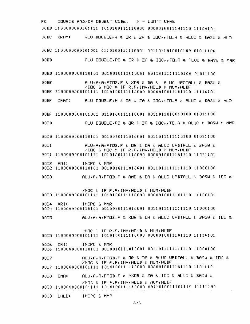
PC SOURCE AND/OR OBJECT CODE. ,x, = DON ,. T CARE
OOBB 1100000000101111 1010100111110000 0000010011101110 11100101
oOBC :x:RAM: ALU DDUBLE,H & DR & ZA & IDC"TD.A & ALUC & BASW & HLD
OOBC 1100000000101001 0110100111110001 0011011010010100 01011100
OOBD ALU DDUBLE,PC & DR & ZA & IOC"TD.A & ALUC & BASW & MMR
OOBD 1100000000110101 0010010111010001 0011011111110100 01011100
OOBE ALU,A,A,FTDB.F & XDR & DA & ALUC UPDTALL & BASW &/IDC & NDC & IF R.F,INV,HDLD & NUM,HLDF
OOBE 1100000000101111 1010100111110000 0000010011101110 11110101
OOBF DRAM: ALU DDUBLE,H & DR & ZA & IDC"TD.A & ALUC & BASW & HLD
OOBF 1100000000101001 0110100111110001 0011011010010100 01011100
OOCO ALU DDUBLE,PC & DR & ZA & IDC"TD.A & ALUC & BASW & MMR
OOCO 1100000000110101 0010010111010001 0011011111110100 01011100
OOCl ALU,A,A,FTDB.F & DR & DA & ALUC UPDTALL & BASW &/IDC & NDC & IF R.F,INV,HDLD & NUM,HLDF
OOCl 1100000000101111 1010100111110000 0000010011101110 11011101
oOC2 AN I : I tiCPC :~ MMR00C2 1100000000110101 0010010111010001 0011011111111110 11000100
00C3 ALU,A,A,FTDB.F & AND & DA & ALUC UPDTALL & BASW & IDC &
/NDC & IF R.F,INV,HDLD & NUM,HLDF00C3 1100000000101111 1010100111110000 0000010011101110 11100101
00C4 XRI: INCPC & MMR00C4 1100000000110101 0010010111010001 0011011111111110 11000100
00C5 ALU,A,A,FTDB.F & XDR & DA & ALUC UPDTALL & BASW & IDC &
/NDC & IF R.F,INV,HDLD & NUM,HLDF00C5 1100000000101111 1010100111110000 0000010011101110 11110101
00C6 DRI: INCPC & MMR00C6 1100000000110101 0010010111010001 0011011111111110 11000100
00C7 ALU,A,A,FTDB.F & DR & DA & ALUC UPDTALL & BASW & IDC &/NDC & IF R.F,INV,HDLD & NUM,HLDF
00C7 1100000000101111 1010100111110000 0000010011101110 11011101
00C8 CMA: ALU,A,A,FTDB.F & NXDR & ZA & IDC & ALUC & BASW &/NDC & IF R.F,INV,HDLD & NUM,HLDF
00C8 1100000000101111 1010100111110000 0011010011101110 11111100
oOC'~ LHLII: I NCPC g.: MMR
A-18

PC SOURCE AND...... OR OB.JECT COIlE. ::< = DON " T CARE00C9 1100000000110101 0010010111010001 0011011111111110 11000100
OOCA ALU·DOUBLE",FTOB.F & DR & DZ & ALUC & BASW & IOC & HLD
OOCA 1100000000101001 0110100111110000 0011011101010100 11011111
OOCB INCPC & MMROOCB 1100000000110101 0010010111010001 0011011111111110 11000100
OOCC ALU",FTOB.F & DR & DZ & ALUC & BASW & IOC & HLD
OOCC 1100000000101001 0110100111110000 0011010101010100 11011111
OOCD ALU DOUBLE",FTOB.F & DR & ZA & ALUC & IOC"TO.A &---BAS:!.,) & HLD
OOCD 1100000000101001 0110100111110001 0011011101010100 11011100
OOCE NALU & IOC & MEMR & IF,INV,READY & NUM, $OOCE 1100001100111000 0010010111010000 0011010101010100 01XXXXXX
OOCF ALU"L,FTOB.F & DR & DZ & IOC & BASW & ALUC & HLDOOCF 1100000000101001 0110100111110000 0011010101001010 11011111
OODO ALU DOUBLE",FTOB.F & PLUS & ALUC & BASW & IOC"TO.A & H
LD/ g< ZAOODO 1100000000101001 0110100111110001 0011011101010100 11000100
00D1 ALU DOUBLE,PC & DR & ZA & IOC"TO.A & BASW & ALUC &/MEMR & IF,INV,READY & NUM , $
OODl 1100001101000100 0010010111010001 0011011111110100 01011100
00D2 ALU"H,FTOB.F & DR & DZ & IOC & BASW & ALUC &/NOC & IF R.F,INV,HOLD & NUM,HLDF
00D2 1100000000101111 1010100111110000 0011010101001000 11011111
00D3 SHLD: INCPC & MMR00D3 1100000000110101 0010010111010001 0011011111111110 11000100
ALU DOUBLE",FTOB.F & DR & DZ & ALUC & BASW & IOC & HLD
00D4 1100000000101001 0110100111110000 0011011101010100 11011111
00D5 INCPC & MMR00D5 1100000000110101 0010010111010001 0011011111111110 11000100
00D6 ALU",FTOB.F & DR & DZ & ALUC & BASW & IOC & HLD00D6 1100000000101001 0110100111110000 0011010101010100 11011111
OOD? ALU DOUBLE",FTOB.F & DR & ZA & ALUC & IOC"TO.A &.····BAS:I.•.1 ::~: HLII
OOD? 1100000000101001 0110100111110001 0011011101010100 11011100
OODS ALU DOUBLE,H & DR & ZA & IOC"TO.D & BASW & ALUC & HLDOODS 1100000000101001 0110100111110000 1011011010010100 01011100
OOD'~ NALU & IOC,DL & MEMW & IF,INV,READV & NUM, $00D9 1100001101100100 0010010111100010 0011010101010100 01XXXXXX
iL10
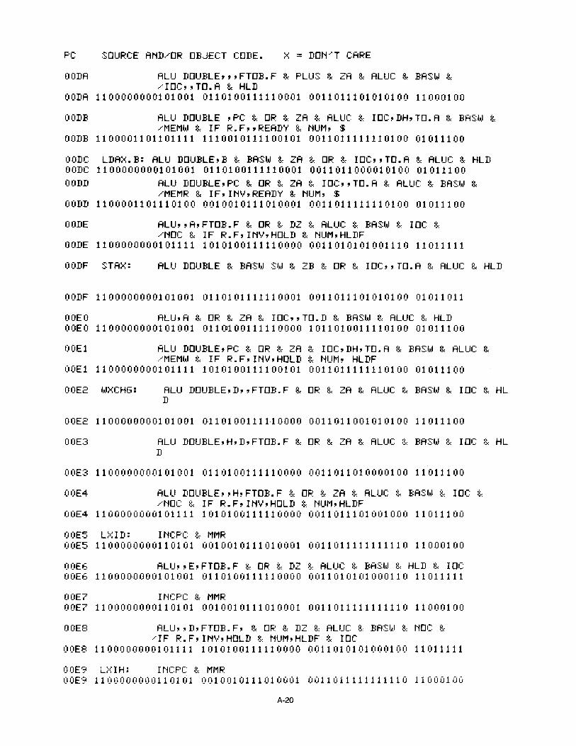
PC SOURCE AND/OR OBJECT CODE. ::< = DON,oT CARE
OODA ALU DOUBLE",FTOB.F & PLUS & ZA & ALUC & BASW &/IOC"TO.A & HLD
OODA 1100000000101001 0110100111110001 0011011101010100 11000100
OODB ALU DOUBLE ,PC & DR & ZA & ALUC & IOC,DH,TO.A & BASW &/MEMW & IF R.F"READY & NUM, $
OODB 1100001101101111 1110010111100101 0011011111110100 01011100
OODC LDAX.B: ALU DOUBLE,B & BASW & ZA & DR & IOC"TO.A & ALUC & HLDOODC 1100000000101001 0110100111110001 0011011000010100 01011100OODD ALU DOUBLE,PC & DR & ZA & IOC"TO.A & ALUC & BASW &
/MEMR & IF,INV,READY & NUM, $OODD 1100001101110100 0010010111010001 0011011111110100 01011100
OODE ALU"A,FTOB.F & DR & DZ & ALUC & BASW & IOC &/NOC & IF R.F,INV,HOLD & NUM,HLDF
OODE 1100000000101111 1010100111110000 0011010101001110 11011111
OODF STAX: ALU DOUBLE & BASW SW & ZB & DR & IOC"TO.A & ALUC & HLD
OODF 1100000000101001 0110101111110001 0011011101010100 01011011
OOEO ALU,A & DR & ZA & IOC"TO.D & BASW & ALUC & HLDOOEO 1100000000101001 0110100111110000 1011010011110100 01011100
OOEl ALU DOUBLE,PC & DR & ZA & IOC,DH,TO.A & BASW & ALUC &/MEMW & IF R.F,INV,HOLD & NUM, HLDF
OOEl 1100000000101111 10101001111QOI0l 001101111111010Q 01011100
ALU DOUBLE,D"FTOB.F & DR & ZA & ALUC & BASW & IOC & HLD
00E2 1100000000101001 0110100111110000 0011011001010100 11011100
OOE:3 ALU DOUBLE,H,D,FTOB.F & DR & ZA & ALUC & BASW & IOC & HLD
OOE:3 1100000000101001 0110100111110000 0011011010000100 11011100
00E4 ALU DOUBLE"H,FTOB.F & DR & ZA & ALUC & BASW & IOC &/NOC & IF R.F,INV,HOLD & NUM,HLDF
00E4 1100000000101111 1010100111110000 0011011101001000 11011100
00E5 LXID: INCPC & MMR00E5 1100000000110101 0010010111010001 0011011111111110 11000100
00E6 ALU"E,FTOB.F & DR & DZ & ALUC & BASW & HLD & IOC00E6 11000GOOOOI01001 0110100111110000 0011010101000110 11011111
OOE? INCPC & MMROOE? 1100000000110101 0010010111010001 0011011111111110 11000100
00E8 ALU"D,FTOB.F, & DR & DZ & ALUC & BASW & NOC &'IF R.F,INV,HOLD & NUM,HLDF & IOC
00E8 1100000000101111 1010100111110000 0011010101000100 11011111
oOE'==, L:':: I H: HiCPC :!,: MMR00E9 1100000000110101 0010010111010001 0011011111111110 11000100
A-20

PC SOURCE AND/OR OBJECT CODE. x = DON~T CARE
OOEA ALU"L,FTOB.F & OR & DZ & ALUC & BASW & HLD & IOCOOEA 1100000000101001 0110100111110000 0011010101001010 11011111
OOEB INCPC & MMROOEB 1100000000110101 0010010111010001 0011011111111110 11000100
OOEC ALU"H,FTOB.F, & OR & DZ & ALUC & BASW & NOC &/IF R.F,INV,HOLD & NUM,HLDF & IOC
OOEC 1100000000101111 1010100111110000 0011010101001000 11011111
OOED LXISP: INCPC & MMROOED 1100000000110101 0010010111010001 0011011111111110 11000100
OOEE ALU DOUBLE"SP,FTOB.F & OR & DZ & ALUC & BASW & HLD & 10C
OOEE 1100000000101001 0110100111110000 0011011101010000 11011111
OOEF INCPC & MMROOEF 1100000000110101 0010010111010001 0011011111111110 11000100
OOFO ALU"SP,FTOB.F, & OR & DZ & ALUC & BASW & NOC &/IF R.F,INY,HOLD & NUM,HLDF & IDe
OOFO 1100000000101111 1010100111110000 0011010101010000 11011111
OOFI INXD: ALU DOUBLE"D,FTOB.F & PLUS & ZB & ALUC & BASW & IOC & HLD
OOFI 1100000000101001 0110100111110000 0011011101000100 11000011
00F2 ALU DOUBLE,D,E,FTOB.A & OR & DZ & ALUC,SWAP & BASW &/IOC & NOC & IF R.F,INY,HOLD & NUM,HLDF
00F2 1100000000101111 1010100111110000 0011111001000110 10011111
00F3 INXH: ALU DOUBLE"H,FTOB.F & PLUS & ZB & ALUC & BASW & IOC & HLD
00F3 1100000000101001 0110100111110000 0011011101001000 11000011
00F4 ALU DOUBLE,H,L,FTOB.A & OR & DZ & ALUC,SWAP & BASW &/IOC & NOC & IF R.F,INY,HOLD & NUM,HLDF
00F4 1100000000101111 1010100111110000 0011111010001010 10011111
00F5 INXSP: ALU DOUBLE"SP,FTOB.F & PLUS & ZB & ALUC & BASW & IOC &
OOF?
/NOC & IF R.F,INV,HOLD & NUM,HLDF00F5 1100000000101111 1010100111110000 0011011101010000 11000011
00F6 DCXD: ALU DOUBLE"D,FTOB.F & SUNIM & ZB & ALUC"CNL &/BASW & IOC & HLD
00F6 1100000000101001 0110100111110000 0011001101000100 11001011
ALU DOUBLE,D,E,FTOB.A & OR & DZ & ALUC,SWAP ~: IOC &/NOC & IF R.F,INV,HOLD & NUM,HLDF
OOF? 1100000000101111 101010XI11110000 OXI1111001000110 10011111
00F8 DCXH: ALU DOUBLE"H,FTOB.F & SUNIM & ZB & ALUC"CNL &~BASW & IDC & HLD
A-21

PC SOURCE AND/OR OBJECT CODE.
00F8 1100000000101001 0110100111110000 0011001101001000 11001011
00F9 ALU DOUBLE,H,L,FTOB.A & DR & DZ & ALUC,SWAP & IOC &/NOC & IF R.F,INV,HOLD & NUM,HLDF
00F9 1100000000101111 101010XIIIII0000 OXIIIII0I000I0I0 10011111
OOFA DCXSP: ALU DDUBLE~~SP~FTOB.F & SUNIM & ZB & ALUC~~CNL &/BASW & IOC & NOC & IF R.F,INV,HOLD & NUM,HLDF
OOFA 1100000000101111 1010100111110000 0011001101010000 11001011
OOFB POP.D: ALU DOUBLE,SP,SP,FTOB.A & DR & ZA & ALUC & BASW &/IOC"TO.A & NOC & IF C.SBR"HOLD & NUM,HLDSB
OOFB 1100000000101001 0110100111110001 0011011100010000 10011100
OOFC ALU DOUBLE,SP,SP,FTOB.F & PLUS & ZA & ALUC & BASW &/ IOC"TO.A & MEMR & IF C.SBR,INV,READY & NUM,MMRSP
OOFC 1100000001000101 0010010111010001 0011011100010000 11000100
OOFD ALU"E,FToB.F & DR & DZ & ALUC & IOC & BASW & HLDOOFD 1100000000101001 0110100111110000 0011010101000110 11011111
OOFE ALU DOUBLE,SP,SP,FTOB.F & PLUS& ZA & ALUC & BASW &/IoC"TO.A & MEMR & IF C.SBR,INV,READY & NUM,MMRSP
OOFE 1100000001000101 0010010111010001 0011011100010000 11000100
OOFF ALU"D,FTOB.F & DR & DZ & ALUC & IOC & BASW & HLDOOFF 1100000000101001 0110100111110000 0011010101000100 11011111
0100 ALU DOUBLE,PC & DR & ZA & ALUC & IOC"TO.A & BASW &/NoC & IF R.F,INV,HOLD & NUM,HLDF
0100 1100000000101111 1010100111110001 0011011111110100 01011100
0101 PoP.H: ALU DOUBLE,SP,SP,FToB.A & DR & ZA & ALUC & BASW &/IoC"TO.A & NOC & IF C.SBR, ,HOLD & NUM,HLDSB
0101 1100000000101001 0110100111110001 0011011100010000 10011100
0102 ALU DOUBLE,SP,SP,FToB.F & PLLIS & ZA & ALUC & BASW &/ IOC"TO.A & MEMR & IF C.SBR,INV,READY & NUM,MMRSP
0102 1100000001000101 0010010111010001 0011011100010000 11000100
0103 ALU"L,FTOB.F & DR & DZ & ALUC & IoC & BASW & HLD0103 1100000000101001 0110100111110000 0011010101001010 11011111
0104 ALU DOUBLE,SP,SP,FToB.F & PLUS& ZA & ALUC & BASW &/IOC"TO.A & MEMR & IF C.SBR,INV~READY & NUM,MMRSP
0104 1100000001000101 0010010111010001 0011011100010000 11000100
0105 ALU"H,FToB.F & DR & DZ & ALUC & IoC & BASW & HLD0105 1100000000101001 0110100111110000 0011010101001000 11011111
0106 ALU DoUBLE,PC & OR & ZA & ALUC & IoC"To.A & BASW &/NoC & IF R.F,INV,HoLD & NUM,HLDF
0106 1100000000101111 1010100111110001 0011011111110100 01011100
0107 JNZ: NALU & IDe & NoC & IF ,INV,Z & NUM,JMP0107 1100000100001000 0000000111110000 0011010101010100 01XXXXXX
0108 INCPC & HLD
A-22

PC SOURCE AND/OR OBJECT CODE. X = DoN~T CARE
0108 1100000000101001 0110100111110001 0011011111111110 11000100
0109 INCPC & IF R.F,INV,HoLD & NUM,HLDF & NoC0109 1100000000101111 1010100111110001 0011011111111110 11000100
010A CNZ: NALU & IoC & NoC & IF ,INV,Z & NUM,CALL010A 1100000100011100 0000000111110000 0011010101010100 01XXXXXX
010B INCPC & HLD010B 1100000000101001 0110100111110001 0011011111111110 11000100
010C INCPC & NoC & IF R.F,INV,HoLD & NUM,HLDF010C 1100000000101111 1010100111110001 0011011111111110 11000100
010D RNZ: NALU & IoC & NoC & IF R.F"Z & NUM,RET010D 1100000101000011 1100000111110000 0011010101010100 01XXXXXX
010E JZ: NALU & IoC & NoC & IF , ,Z & NUM,JMP010E 1100000100001000 0100000111110000 0011010101010100 01XXXXXX
010F INCPC & HLD010F 1100000000101001 0110100111110001 0011011111111110 11000100
0110 INCPC & NoC & IF R.F,INV,HoLD & NUM,HLDF0110 1100000000101111 1010100111110001 0011011111111110 11000100
0111 CZ: NALU & IoC & NoC & IF , ,Z & NUM,CALL0111 1100000100011100 0100000111110000 0011010101010100 01XXXXXX
0112 INCPC & HLD0112 1100000000101001 0110100111110001 0011011111111110 11000100
0113 INCPC & NoC & IF R.F,INV,HoLD & NUM,HLDF0113 1100000000101111 1010100111110001 0011011111111110 11000100
0114 RZ: NALU & IoC & NOC & IF R.F,INV,Z & NUM,RET0114 1100000101000011 1000000111110000 0011010101010100 01XXXXXX
0115 JNC: NALU & IOC & NOC & IF ,INV,CY & NUM,JMP0115 1100000100001000 0000010111110000 0011010101010100 01XXXXXX
0116 INCPC &HLD0116 1100000000101001 0110100111110001 0011011111111110 11000100
0117 INCPC & NoC & IF R.F,INV,HoLD & NUM,HLDF0117 1100000000101111 1010100111110001 0011011111111110 11000100
0118 CNC: NALU & IoC & NOC & IF ,INV,CY & NUM,CALL0118 1100000100011100 0000010111110000 0011010101010100 01XXXXXX
0119 INCPC & HLD0119 1100000000101001 0110100111110001 0011011111111110 11000100
011 A I NCPC 8.: NoC & IF R. F ,I NV, HoLII & NUM, HLDF011A 1100000000101111 1010100111110001 0011011111111110 11000100
011B RNC: NALU & IOC & NoC & IF R.F"CY & NUM,RET011B 1100000101000011 1100010111110000 0011010101010100 01XXXXXX
01IC --IC: NALU & IDC & NDC & IF "CY & NUM,JMP
M-''''

PC SOURCE AND/OR OBJECT CODE. X = DON/T CAREOtlC 1100000100001000 0100010111110000 0011010101010100 01XXXXXX
011D INCPC & HLD011D 1100000000101001 0110100111110001 0011011111111110 11000100
011E INCPC & NOC & IF R.F,INV,HOLD & NUM,HLDF011E 1100000000101111 1010100111110001 0011011111111110 11000100
011F CC: NALU & IOC & NOC & IF "CV & NUM,CALL011F 1100000100011100 0100010111110000 0011010101010100 01XXXXXX
0120 INCPC & HLD0120 1100000000101001 0110100111110001 0011011111111110 11000100
0121 INCPC & NOC & IF R.F,INV,HOLD & NUM,HLDF0121 1100000000101111 1010100111110001 0011011111111110 11000100
0122 RC: NALU & IOC & NOC & IF R.F,INV,CV & NUM,RET0122 1100000101000011 1000010111110000 0011010101010100 01XXXXXX
0123 JPO: NALU & IDC & NOC & IF',INV,P & NUM~JMP
012~ 1100000100001000 0000100111110000 0011010101010100 01XXXXXX
0124 INCPC & HLD0124 1100000000101001 0110100111110001 0011011111111110 11000100
0125 INCPC & NOC & IF R.F,INV,HOLD & NUM,HLDF0125 1100000000101111 1010100111110001 0011011111111110 11000100
0126 CPO: NALU & IOC & NOC & IF ,INV,P & NUM,CALL0126 1100000100011100 0000100111110000 0011010101010100 01XXXXXX
0127 INCPC & HLD0127 1100000000101001 0110100111110001 0011011111111110 11000100
0128 INCPC & NOC & IF R.F,INV,HOLD& NUM,HLDF0128 1100000000101111 1010100111110001 0011011111111110 11000100
0129 RPO: NALU & IOC & NOC & IF R.F"P & NUM,RET0129 1100000101000011 1100100111110000 0011010101010100 01XXXXXX
012A JPE: NALU & IOC & NOC & IF "P & NUM,JMP012A 1100000100001000 0100100111110000 0011010101010100 01XXXXXX
012B INCPC & HLD012B 1100000000101001 0110100111110001 0011011111111110 11000100
012C INCPC & NOC &IF R.F,INV,HOLD & NUM,HLDF012C 1100000000101111 1010100111110001 0011011111111110 11000100
012D CPE: NALU & IOC & NOC & IF "P & NUM,CALL012D 1100000100011100 0100100111110000 0011010101010100 01XXXXXX
012E INCPC & HLD012E 1100000000101(ft'1 0110100111110001 0011011111111110 11000100
012F INCPC & NOC & IF R.F,INV,HDLD & NUM,HLDF012F 1100000000101111 1010100111110001 0011011111111110 11000100
0130 RPE: NALU & IOC & NOC & IF R.F,INV,P & NUM,RET
A~4

PC SOURCE AND/OR OBJECT CODE.
0130 1100000101000011 1000100111110000 0011010101010100 01XXXXXX
0131 Jp: NALU & IOC & NOC & IF ,INV,S & NUM,JMP0131 1100000100001000 0000110111110000 0011010101010100 01XXXXXX
0132 INCPC & HLD0132 1100000000101001 0110100111110001 0011011111111110 11000100
0133 INCPC & NoC & IF R.F,INV,HoLD & NUM,HLDF0133 1100000000101111 1010100111110001 0011011111111110 11000100
0134 CP: NALU & IoC & NoC & IF R.F"S & NUM,CALL0134 1100000100011111 1100110111110000 0011010101010100 01XXXXXX
0135 INCPC & HLD0135 1100000000101001 0110100111110001 0011011111111110 11000100
0136 INCPC & NoC & IF R.F,INY,HoLD & NUM,HLDF0136 1100000000101111 1010100111110001 0011011111111110 11000100
0137 RP: NALU & IoC & NoC & IF ,INV,S & NUM,RET0137 1100000101000000 0000110111110000 0011010101010100 01XXXXXX
0138 JM: NALU & IoC & NoC & IF "S & NUM,JMP0138 1100000100001000 0100110111110000 0011010101010100 01XXXXXX
0139 INCPC & HLD0139 1100000000101001 0110100111110001 0011011111111110 11000100
013A INCPC & NoC & IF R.F,INY,HoLD & NUM,HLDF013A 1100000000101111 1010100111110001 0011011111111110 11000100
013B CM: NALU & IoC & NoC & IF "S & NUM,CALL013B 1100000100011100 0100110111110000 0011010101010100 01XXXXXX
013C INCPC & HLD013C 1100000000101001 0110100111110001 0011011111111110 11000100
013D INCPC & NoC & IF R.F,INY,HoLD & NUM,HLDF013D 1100000000101111 1010100111110001 0011011111111110 11000100
013E RM: NALU & IoC & NoC & IF R.F,INV,S & NUM,RET013E 1100000101000011 1000110111110000 0011010101010100 01XXXXXX
013F DAR: NALU & IoC & HLD013F 1100000000101001 0110100111110000 0011010101010100 01XXXXXX
0140 NALU & IoC & IF,INV & NUM DBUS, 006 & NoC0140 1000000000011000 0011110111110000 0011010101010100 01XXXXXX
0141 ALU",FToB.F & OR & DZ & ALUC & BASW & IoC &/NoC & IF"AC & NUM,DAAl
0141 1100010100011000 0101000111110000 0011010101010100 11011111
0142 NALU & IoC & IF,INV & NUM DBUS,OOF & NoC0142 1000000000111100 0011110111110000 0011010101010100 01XXXXXX
0143 ALU,A"FToQ & AND & DA & ALUC & BASW & IoC &/NoC & IF,INY & NUM DBUS,OOA
0143 1000000000101000 0011110111110000 0011010011110100 00100101
A-?~

PC SOURCE AND/OR OBJECT CODE. ::-:; = DDt'! ..' T CAF.~E
0144 ALU & DQ & SUNIM & ALue & BASW & IDe & HLD0144 1100000000101001 0110100111110000 0011010101010100 01001110
0145 NALU & IOC & NOC & IF,INV,CN.4 & NUM,$+20145 1100010100011100 0011100111110000 0011010101010100 01XXXXXX
0146 DAA1: ALU"A,FTOB.F & PLUS & AB & ALUC UPDTALL"CNL &/IOC & BASW & NOC & IF C.SBR"CY & NUM,DAA4
0146 1100010101111101 0100010111110000 0000000101001110 11000001
0147 NALU & IOC & IF,INV & NUM DBUS, 060 & NOC0147 1000000110000000 0011110111110000 0011010101010100 01XXXXXX
0148 ALU",FTOB.F & DR & DZ & ALUC & BASW & IOC &/NOC & IF"CY & NUM,DAA3
0148 1100010100111100 0100010111110000 0011010101010100 11011111
0149 NALU & IOC & IF,INV & NUM DBUS,OFO & NOC0149 1000001111000000 0011110111110000 0011010101010100 01XXXXXX
014A ALU,A"FTOQ & AND & DA & ALUC & BASW & IDe &/NOC & IF,INV & NUM DBUS,OAO
014A 1000001010000000 0011110111110000 0011010011110100 00100101
014B ALU & DQ & SUNIM & ALUC & BASW & IDC & HLD014B 1100000000101001 0110100111110000 0011010101010100 01001110
014C NALU & IOC & NOC & IF,INV,CN~4 & NUM,$+2014C 1100010100111000 00111001111100000011010101010100 0IX;:.:X:X::X::X:
014D DAA2: ALU"A,FTDB.F & PLUS & AB & ALUC UPDTALL "CNL &/BASW & IOC & HLD
014D 1100000000101001 0110100111110000 0000000101001110 11000001
014E NALU & IOC & NOC & IF R.F,INV,HDLD & NUM,HLDF014E 1100000000101111 1010100111110000 0011010101010100 01XXXXXX
014F DAA3: ALU"A,FTOB.F & PLUS & AB & ALUC UPDTFL"CNL &/BASW & IOC & NOC & IF R.F,INV,HOLD & NUM,HLDF
014F 1100000000101111 1010100111110000 0010000101001110 11000001
0150 POP.PSW: ALU DDUBLE,SP,SP,FTOB.A & DR & ZA & ALUC & BASW & IOC"TO. A :~.: .····t'!OC :~.: IF C. SBR, ,HOLD :~ NUM, HLD:S:B
0150 1100000000101001 0110100111110001 0011011100010000 10011100
0151 ALU DOUBLE,SP,SP,FTOB.F & PLUS & ZA & ALUC & BASW & MEMR
&/IOC"TO.A & IF C.SBR,INV,READY & NUM,MMRSP0151 1100000001000101 0010010111010001 0011011100010000 11000100
0152 ALU & NAND & ALUC & IOC & BASW & HLD0152 1100000000101001 0110100111110000 0011010101010100 01101XXX
0153 ALU DDUBLE,SP,SP,FTDB.F & PLUS & ZA & ALUC & BASW &/IOC"TO.A & MEMR & IF C.SBR,INV,READY & NUM,MMRSP
0153 1100000001000101 0010010111010001 0011011100010000 11000100
0154 ALU"A,FTDB.F & DR & DZ & ALUC & BASW & IDe & HLD
A-26
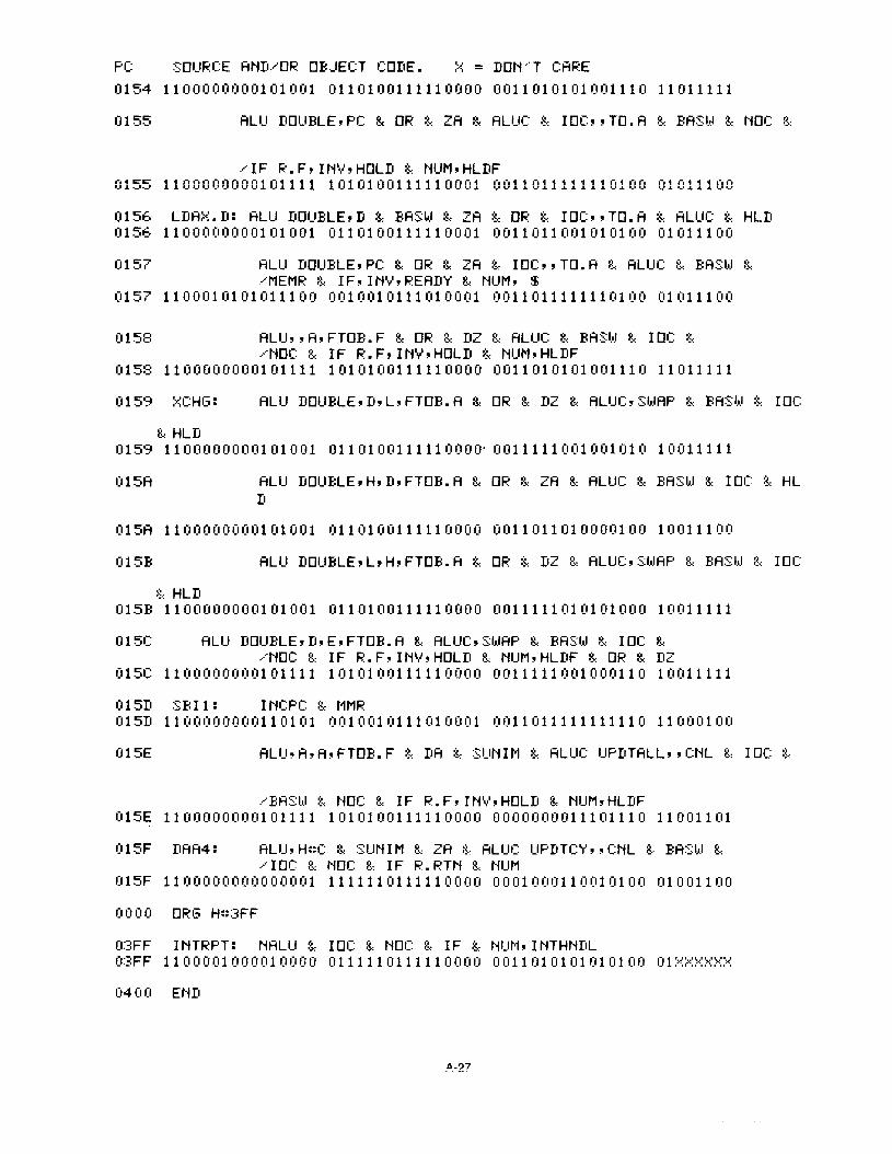
PC SOURCE AND/OR OBJECT CODE.
0154 1100000000101001 0110100111110000 0011010101001110 11011111
0155 ALU DOUBLE,PC & DR & ZA & ALUC & IOC"TO.A & BASW & NOC &
1100000000101111 1010100111110001 0011011111110100 ,-, 1 '-I 1 1 1 ,-,,-,I.... .&. I_' ......... ' ..' ' ..'
0156 LDAX.D: ALU DOUBLE,D & BASW & ZA & DR & IDC"TD.A & ALUC & HLD0156 1100000000101001 0110100111110001 0011011001010100 01011100
0157 ALU DDUBLE,PC & DR & ZA & IDC"TD.A & ALUC & BASW &/MEMR & IF,INV,READY & NUM, $
0157 1100010101011100 0010010111010001 0011011111110100 01011100
0158 ALU"A,FTOB.F & DR & DZ & ALUC & BASW & IDC &/NOC & IF R.F,INV,HOLD & NUM,HLDF
0158 1100000000101111 1010100111110000 0011010101001110 11011111
0159 ::-::CHG: ALU DDUBLE,D,L,FTDB.A & DR & DZ & ALUC,SWAP & BASW & IOC
& HLD0159 1100000000101001 0110100111110000· 0011111001001010 10011111
015A ALU DDUBLE,H,D,FTDB.A & DR & ZA & ALUC & BASW & IDC & HLII
015A 1100000000101001 0110100111110000 0011011010000100 10011100
015B
g.: HLD015B 1100000000101001 0110100111110000 0011111010101000 10011111
015C ALU DDUBLE,D,E,FTDB.A & ALUC,SWAP & BASW & IDC &/NDC & IF R.F,INV,HOLD & NUM,HLDF & DR & DZ
015C 1100000000101111 1010100111110000 0011111001000110 10011111
015D SBll: INCPC & MMR015D 1100000000110101 0010010111010001 0011011111111110 11000100
015E ALU,A,A,FTDB.F & DA & SUNIM & ALUC UPDTALL"CNL & IDC &
/BASW & NDC & IF R.F,INV,HOLD & NUM,HLDF015E 1100000000101111 1010100111110000 0000000011101110 11001101
o15F DAA4: ALU, H~~C :~, :S:UN I M 8.: ZA :~, ALUC UPItTC'y'" CNL ~., BAS:lt.1 8.,/IDC & NOC & IF R.RTN & NUM
015F 1100000000000001 1111110111110000 0001000110010100 01001100
0000 ORI3 H~~:3FF
03FF INTRPT: NALU & IDe & NOC & IF & NUM,INTHNDL03FF 1100001000010000 0111110111110000 0011010101010100 01XXXXXX
0400 END

APPENDIX IIIMapping PROM AMDASM Output
esc File Name: AMMAPO
Note: A listing of the Mapping PROM Source Code (Assembly File) only may be obtainedusing CSC File Name AMMAPA.
A-28
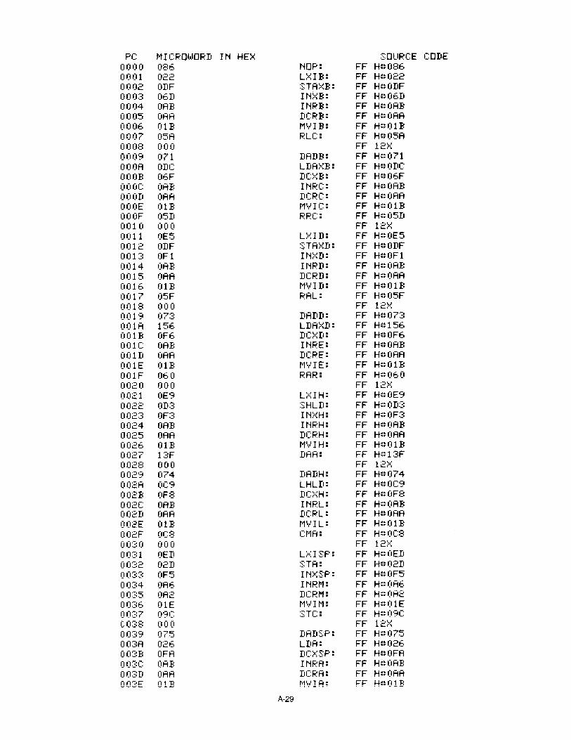
PC MI CROI.t.lORIt IN HEX SOURCE COIlE0000 08E. t"iOP: FF H~~086
0001 022 U-::IB: FF H~~022
0002 ODF :S:TA:'-::B: FF H~~ OIIF000:3 06D IN::-::B: FF H~~ 06D0004 OAB INRB: FF H~~OAB
0005 OAA DCRB: FF H~~OAA
OOOE. 01B M'·'" I B: FF H~~ 01 B0007 05A ~., .-.. FF H~~ 05A'.LI_" •
0008 000 FF 1"=-'x'L... ••
000':;' 071 DADB: FF H~~ 071OOOA ODC LDA~"':B: FF H~~ODC
OOOB 06F DC:=-::B: FF H~~OE.F
OOOC OAB INRC: FF H~~OAB
OOOD OAA DCRC: FF H~~OAA
OOOE 01B MVIC: FF H~~O lBOOOF 05D RRC: FF H~~05II
0010 000 FF 12:=-::0011 OE5 L:~~ I D: FF H~~OE5
0012 ODF :S:TA::<:D: FF H~~ODF
001:~: OFl I I'i:>::n: FF H~~ OF 10014 OAB INRII: FF H~~OAB
0015 OAA DCRII: FF H~~OAA
0016 01B M'·."I II: FF H~~O lB0017 05F RAL: FF H~~05F
0018 000 FF 12X0019 07:3 DADII: FF H~~ 07:3001A 156 LIIA:>m: FF H~~156
001B OF6 Dc;-::I1: FF H~~OF6
001C OAB I t"iRE: FF H~~OAB
001D OAA DCRE: FF H~~OAA
001E 01B t'lV IE: FF H~~O lB001F 060 RAR: FF H~~060
0020 000 FF l"=-v11- •• ',
0021 OE9 U<IH: FF H~~OE9
0022 OD:3 SHLD: FF H~~ OD:3002:3 OF:3 IN:X:H: FF H~~ OF:30024 OAB I N~~H: FF H~~OAB
0025 OAA DC~~H: FF H~~OAA
0026 01B MVIH: FF H~~ 0 lB0027 1:3F DAA: FF H~~ l:3F002:;:: 000 FF 1.=- 'x'L... ••
002':;' 074 DAIIH: FF H~~ 074002A OC':;' LHLD: FF H~~OC9
002B OF8 DC::<H: FF H~~OF8
002C OAB II'iRL: FF H~~ OAB002D OAA DCRL: FF H~~ OAA002E 01B t'lV I L: FF H~~ 0 1B002F OC8 CMA: FF H~~ OC800:30 000 FF 12;-::00:31 OED U-:: I :S:P: FF H~~OEII
00:32 02D STA: FF H~~ 02I100:3:3 OF5 I N:x:S:P: FF H~~OF5
00:~:4 OA6 INRM: FF H~~OA6
00:35 OA2 DCRM: FF H~~ OA200:36 OlE t·l '·,.' 1M: FF H~~ OlE00:37 09C STC: FF H~~ 09CCO:38 000 FF l'=-'x'L... ••
0IJ3':;' 075 DAD:S:P: FF H~~ 075OO:3A 026 LIlA: FF H~~02E.
OO:3B OFA DC:>:::S:P: FF H~~OFA
OO:3C OAB INRA: FF H~~OAE:
OO:3D OAA DCRA: FF H~~ OAA003E OlB t·l '·/! A: FF H~~ (I l:B
A-29
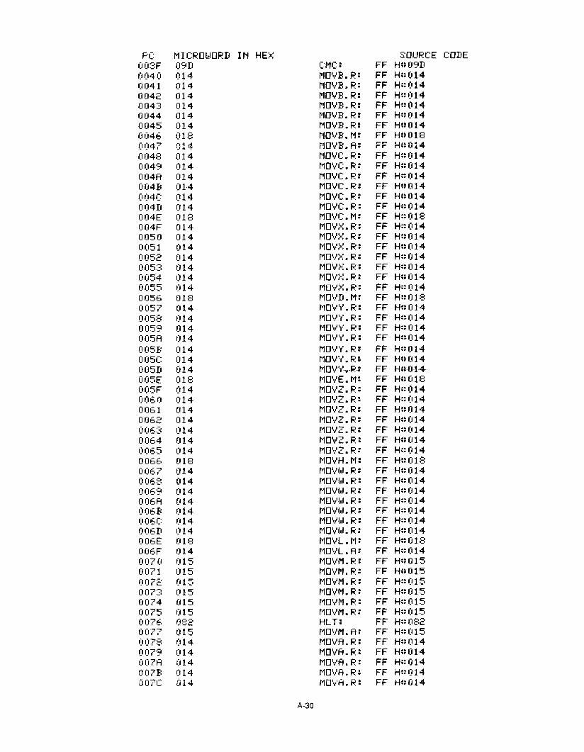
PC MI CROb.IORI! IN HE>r: S:OURCE COIlEOO:=:F 09D CMC: FF H~~09D
0040 014 MOVB.R: FF H~~014
0041 014 MOVB.R: FF H~~014
0042 014 MOVB.R: FF H~~O140043 014 MO.....B.R: FF H~~014
0044 014 t·1O .....B. R: FF H~~014
0045 014 MO.....B.R: FF H~~014
004E. 018 MO.....B.M: FF H~~O180047 014 t10..... B. A: FF H~~014
0048 014 MOVC.R: FF H~~O140049 014 MOVC.R: FF H~~O14004A 014 MOVC.R: FF H~014
004B 014 I"1O .....C. R: FF H~~014
004C 014 MO.....C.R: FF H~~014
004D 014 MO'·...C. R: FF H~~014
004E 018 MOVC.M: FF H~~O18004F 014 MO ..... :x:. R: FF H~~014
0050 014 MO.....X.R: FF H~::014
0051 014 t10'·... :x:. R: FF H~~O140052 014 MO..... :x:. R: FF H~~O140053 014 MO..... ;:.':. R: FF H~~O140054 014 MO',,,,:x: • R: FF H:;~O140055 014 MOV;'c:. R: FF H~~ 0 140056 018 MOVD.M: FF H~~O180057 014 I"1OV'-(. ~:: FF H~~ 0140058 014 MOV'l. R: FF H~~014
0059 014 1"10'.1')"'. R: FF H~~014
005A 014 MOV'-(. R: FF H~~014
005B 014 MO'·,"'Y'. R: FF H~~014
005C 014 t10..... Y. R: FF H~~014
005B 014 MDV'-(.R: FF H~-(I-14
005E 018 I"1OVE. M: FF H~~018
005F 014 MOVZ.R: FF H~~014
0060 014 I"1OVZ. R: FF H~~014
0061 014 I"1O'·...Z. R: FF H:~014
0062 014 MOVZ.R: FF H~~014
0063 014 MOVZ.R: FF H~~014
0064 014 t10 ..... Z • R: FF H~~014
0065 014 MO'·...Z. R: FF H~~014
0066 018 MOVH.M: FF H~~018
0067 014 MOVh.l. ~:: FF H~~0.14
0068 014 t10VI}.I. R: FF H~~ 0 140069 014 t·1OVh... R: FF H~~014
OOE.A 014 t·1O ...·'h;!. R: FF H~::O14006B 014 MOVI}.I. R: FF H~~014
006C 014 I"1OVI}.I. R : FF H~::014
OOE.D 014 MOVh.l. R: FF H:::014OOE.E 018 MOVL.I'l: FF H~::018
006F 014 I"1O',"'L. A: FF H~::O140070 015 MOVM.R: FF H:::0150071 015 MO"lM. R: FF H~~O150072 015 I"1OVM. R: FF H:~ 0 150073 015 I"1OVM. R: FF H~::015
0074 015 MO.....M.R: FF H:::0150075 015 I"1OVM. R: FF H~::015
0076 082 HLT: FF H~::082
0077 015 t·1O',...M. A: FF H~:: 0150078 014 t10VA. R: FF H::: 0 140079 014 t10VA. R: FF H~~014
007A 014 MOVA. F.~: FF H~~O14007B 014 t'1O ...·'A. ~~: FF H:~ 0 1401)7C 014 t10'·,'A. R: FF H:::O 14
A·30

PC MI CR0 II.IORIt IN HE>c: SOURCE CoItE007I1 014 MoVA.R: FF H~~014
007E 018 MoVA.M: FF H~~O 18007F 014 /'1OVA. A: FF H~~O 140080 t):34 ADDR: FF H~~034
0081 034 ADItR: FF H~~034
0082 034 AItItR: FF H~~034
0083 034 AItItR: FF H~~034
0084 0:34 AItItR: FF H~~034
0085 034 AIIItR: FF H~~0:34
008E. 035 AItItM= FF H~~035
0087 034 AItIIA: FF H~~034
00B8 0:3A AItCR: FF H~~ 0:3A00$9 03A AItCR: FF H~~03A
008A 03A AItCR: FF H~~03A
OOBE: 03A ADCR: FF H~~03A
008C 03A ADCR: FF H~~03A
OOBD 0:3A ADCR: FF H~~03A
OOBE 03(: ADCM: FF H~~0:3C
OOBF O:~:A ADCA: FF H~0:3A
0090 OAC SUE:R: FF H~~OAC
0091 OAC :S:UBR: FF H~~OAC
0092 OAC :S:UBR: FF H~~OAC
O(I':;':~: OAC :S:UBR: FF H~~OAC
0094 OAC :S:UBR: FF H~~OAC
0095 OAC :S:UBR: FF H~~OAC
0096 OAD :S:UBM: FF H~~OAD
0097 OAC S:UBA: FF H~OAC
0098 OB2 SBBR: FF H~~OB2
0099 OB2 :S:BBR: FF H~~OB2
009A OB2 :~~BBR: FF H~~OB2
009B OB2 :S:BBR: FF H~~OB2
009C OB2 :S:BBR: FF H~~ OB2009n OB2 :S:BBR: FF H~~OB2
009E OB4 :S:BBM: FF H~~OB4
009F OB2 :S:BBA: FF H~~ OB2OOAO 09F ANAR: FF H=~O':;'F
OOAl 09F ANAR: FF H~~O':;'F
00A2 09F ANAR: FF H~~09F
00A3 09F ANAR: FF H~~09F
00A4 09F ANAR: FF H~~09F
00A5 09F ANAR: FF H~~09F
00A6 OB9 ANA~l: FF H~~OB9
00A7 09F ANAA: FF H~~ O':;'FOOAB OAO :X:RAR: FF H~~OAO
00A9 OAO >::RAR: FF H~~OAO
OOAA OAO >~RAR: FF H~~OAO
OOAB OAO ;:-::RAR: FF H=~OAO
OOAC OA 0 :X:RAR: FF H~~ OAOOOAn OAO >::RAR: FF H~~OAO
OOAE OBC >::RAM: FF H~~OBC
OOAF OAO ;:-::RAA: FF H=~OAO
OOBO OAl oRAR: FF H~~ OAlOOBl OAl oRAR: FF H=~OAl
00B2 OAl oRAF.~: FF H~~OAl
OOB3 OAl oRAR: FF H~~OAl
OOB4 OAl oRAR: FF H=~ OAl00B5 OAl oRAF.~ : FF H=~ OA 100B6 OBF DRAM: FF H~~ OBFOOB7' OAl DRAA: FF H;'~ OAlOOBB 07E. CMPR: FF H~~ 07'6OOB9 07'6 Ct'lPR: FF H=~ 076OOBA 076 CMPR: FF H~~076
n- ...... '

PC ~1 I CROI).IO~~n IN HE>c: :~:oURCE CoIrEOOBB 076 CMPR: FF H~~076
OOBC 07E. CMPR: FF H~~07E,
001H1 076 CMPR: FF H::~07E.
OOBE 079 CMPM: FF H~079
OOBF 076 CMPA: FF H::~076
OOCO 10D RNZ: FF H~~l onOOCl 07C PoPB: FF H~~07C
00C2 107 .J~C: FF H::~l 07OOC:3 042 JMP: FF H~~042
00C4 lOA C~C: FF H::~l OA00C5 064 PtIS:H~: FF H::~064
OOCE, 0:~:8 ADI: FF H::~0:38
00C7 055 RSTO: FF H::~055
00C8 114 RZ: FF H::~114
00C9 050 RET: FF H::~050
OOCA 10E JZ: FF H::~ 1 OEOOCB 000 FF 12::·~
OOCC 111 CZ: FF H~~111OOCD 047 CALL: FF H::~047
OOCE O:3F ACI: FF H::~0:3F
OOCF 055 RSTl : FF H::~055
OODO llB RNC: FF H::~ llB00n1 OFB PoPD: FF H::~OFB
00D2 115 J~iC: FF H::~115
OOII3 08B OUT. : FF H~~08B
00D4 118 CtiC: FF H::~118
00D5 OEA PUS:HD: FF H::~064
00D6 OBO :~:UI : FF H~~OBO
00D7 055 RST2: FF H::~055
00D8 122 RC: FF H~~122
oOIl', 000 FF 12XCfOIIA llC: JC: FF H~~ llCOODB 087 IN. : FF H::~087
OODC llF CC: FF H~~11 FOODD 000 FF. 12XOODE OB7 sBI: FF H::~OB7
OODF 055 RS:T:3: FF H::~055
OOEO 129 RPo: FF H::~129
OOEl 101 PoPH: FF H::~ 10100E2 12:3 JPo: FF H~~12:3
OOE:3 092 ;;nHL: FF H::~092
00E4 126 CPO: FF H::~12E.
00E5 064 PUSHH: FF H::~064
OOEE. OC2 AtiI: FF H~~OC2
00E7 055 R:~:T4: FF H::~055
00E8 1:30 RPE: FF H~~ 1:30OOE9 09B PCHL: FF H::~09B
OOEA 12A JPE: FF H::~12A
OOEB 15', ::-:;CHI3: FF H~~15',
OOEC 12D CPE: FF H::~12D
OOED 000 FF 12:=-::OOEE OC4 ;:-=;R I: FF H::~OC4
OOEF 055 R:~:T5: FF H::~055
OOFO 1:37 RP: FF H::~ 1:37OOFI 150 PoPPS:ld: FF H~~150
00F2 1:31 JP: FF H~~1:31OOF:3 090 DI: FF H::~090
OOF4 1:34 CP: FF H::~134
00F5 068 PU:S:HPS:I..J : FF H::~068
OOF6 OC6 oRI: FF H::~OC6
OOF7 055 RS:TE,: FF H~~055
OOF8 13E PM: FF H:::l3E
A-32
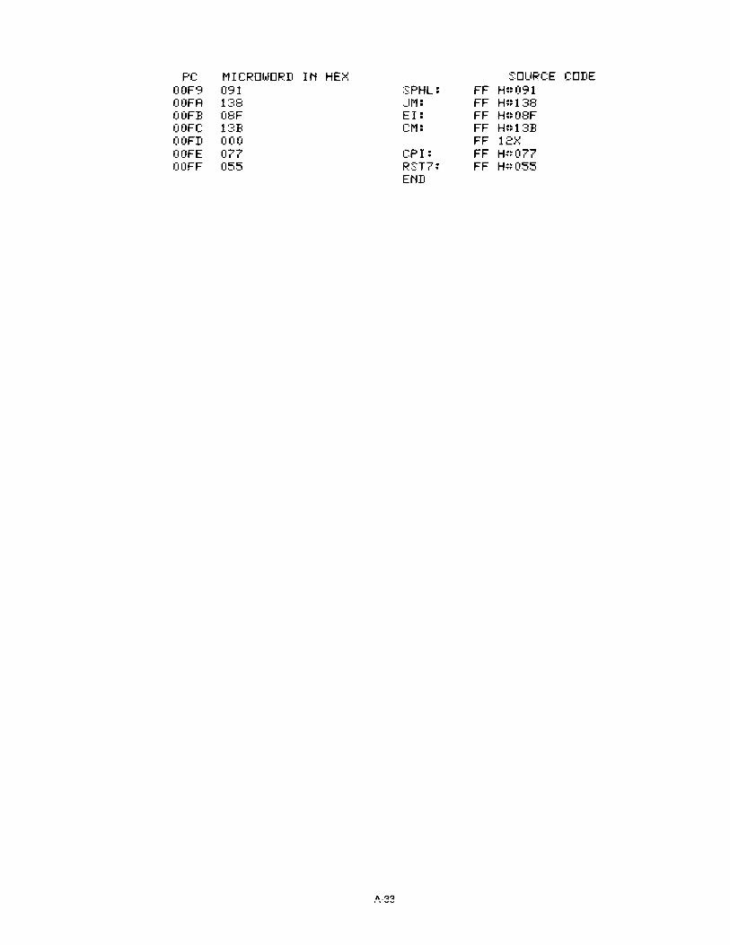
PC t1 I CRol.tJORII IN HE>:: SOURCE COIlE00F'3 0'31 :5:PHL: FF H::~0'31
OOFA 1:~:8 --1M: FF H::~1 :~:8
OOFB 08F EI: FF H::~08F
OOFC 1:3B CM: FF H::~ 1:3BOOFII 000 FF 1 "-=.0 'x'L.., •
OOFE 077 CPI: FF H::~077
OOFF 055 R:5:T7: FF H::~ 055ENII

11DO 0 1 O2 0 3 0 4 0 5 0 6 0 7
CPAm25LS377
U1516
PL55
2 5 6 9 12 15 16 19
15 1 2 3 4 7 6 515 1 2 3 4 7 6 5
.-------------------+_+--;_�I-t-+_+-+------------++.....--------- 6!U65
~----------------++--+---1-I-+-++------------+_++......------- 10!U65
~---------------t__t_-t--+--1-1I-t-+-------------t_t__t_-t-......------ 13/u65
...---------------I-+-++_+--;_II-t--------------;-I-+-++......----- 6!U66
.---------------+-I-+-+++--;_I~-----------_+-+_II-t-+_+......---- 10!U66
...-------------+_I-t-+_++-+--;-------------+-+--;-I-+-++......--- 13!U6615 1 2 3 4 7 6 5
A7 ~ A5 A4 A3 A2 A1 AO13 CS1
A7 A6 A5 A4 A3 A2 A1 Ao13 CS1
A7 A6 A5 A4 A3 A2 A1 Ao13 CS1
14CS2
Am29761U13
14CS2
Am29761U12 14
CS2
Am29761U11
9 10 11 12 9 10 11 12 9 10 11 12
6.8,10.12
Am2909U21
1 6.8,10,1221 20 19 18 22
27 rJ>
1 6,8,10,12
Am2909U23
7 9 11 13 7 9 11 1327 A. r-';"&'-..L.....I""';'.&...;...L.,;...L..;..L".;..&,....., 27
15 0 3 'Y 15 0 3 O21----------:;-;:-1 ZERO t-----------;:;:-i ZERO1- -::1~6 So 16 So
I--------__:~:=_t~ Sl A~~~09 ......--------:~:;.f~Sl
Cn ~23,...---------:~:::-I4 ~P Cn""""23,..--------:~;:;-I: ~P C 23
Y3 Y2 Y1 YO DE RE ORO_ 3 ....Cn_+_4_Y...3_Y...2_Y,.;.1_Y...0;....",O""E_R.,.E_0"l'RO_-......3t-=''----------'""'-I Cn+4 Y3 Y2 Y1 YO DE RE ORO_~ V CC
21 20 19 18 22
7 9 11 13
1Kn
Am29751U14PL40 A2
11A1PL39
10Ao cs
15
-=-
rl A4- 13
PL41 - A312
J1 PROGRAM MEMORY
MPR·452
....'"..J"-
Am2SLS374U3132
74LS04 11
10 Ul12
" to ll) v M N .... 0...J ...J ...J ...J ...J ...J ...J ...J0.. c.. Q. Q. 0.. Q. 0.. Q.
DO 01 02 03 04 05 06 07
CP'1
DO 01 02 03 04 05 06 D711
CP
Am2SLS374U3241
DE
-=- Yo Y1 Y2 Y3 Y4 Y5 Y6 Y7
PL54
Am25LS374U4142
Figure 3.
DO 01 02 D3 04 05 06 D7CP
11
DO 01 02 OJ 04 D5 0 6 D711
CP
Am25LS374U7172
DEPL27
""'"""--U-6S-2~""-__---J
74LS04'""'..J"-
.... '" '" ~'" '" '""- "- "-
DO 01 02 03 04 05 06 D711
CP
Am25LS374U51
DE
-=- YO Y1 Y2 Y3 Y4 Y5 Y6 Y7
.... '" '" ;:!j'" '" '"..J ..J ..J ..J"- "- "- "-
74808
.... '" ... ... 0 en '"'" '" "' ... '" '""- "- "- "- "- "- "-
DO 01 O2 0 3 0 4 05 06 ~11
CP
Am25LS374U5161
DE
-=- Vo Y1 Y2 V3 Y4 YS Y6 Y7
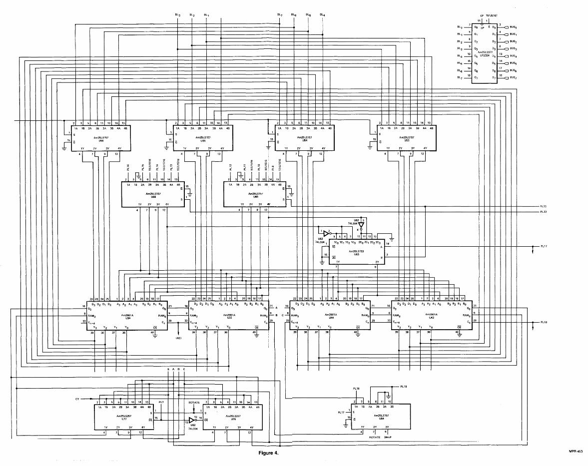
Bl5
ICP 19/US161
111 11
BlO
.......: r-Ou-~"'p"""E-Oo"'NBUSo
Bl l --=. 0, 0 1~ BUS I
Bl2 --=. 02 O2~BU~
Bl3~ 03 0 3~ BUS3
Bl4 ~ 04A~~;~~~7704~ BUS4
Bl5 -2.: Os 0 5~ BUSs
16 17Bl6 - Os 0 6 j---<:J BUS6
Bl7~ 07 0 7~ BUS7
4Y
6 11 10 14 13
2B 3A 3B 4A 4B
Am25lS157U53
2Y 3Y
(G..........,...-:....-;,;-_.;,;..._...;.,..._..J4Y
4A 4B2B 3A 3B
6 11 10 14 13L:lA 31B 52A
Am25lS157r G U54
-=t lY 2Y 3Y
;e ;e ;e4LL~~'" '" '"
,I ,p.;1 .I JJJJ4Y
IlOT 14 13
3Y
61 11
2Y
Am25lS157U55
lY
L2s1A 31B
52A 2B 3A 3B 4A 4B
t G
.....:....-,.;--;,;....-.;,;..-..:,;._...
...J ...J ~ '<t ~ ...J ~
2\ 3~i j j j j J
4Y
6 11 10 14 13
2B 3A 3B 4A 4BL:A 31B :AAm25lS157t G lY 2Y U56 3Y
2A 2B 3A 3B 4AlA 1B 4B
GhAm25lS157 I -b
1Y 2Y U65 3Y IN SnL..__"";'_;;;"""';;';"""";'__-..J '--1-1-1-1----------------++++-........----------+-+-+-+-+-+-+-+----Pl33
lA lB 2A 2B 3A 3B 4A 4B
G~Am25lS157 I ..l..
L--..T---T-U66-T---T-----1S~1-=-_lY 2Y 3Y 4Y
4 7 9 12 L..-t-t-t-t-----...::4+-7+.....::.9+-..:.:12+-----t-t-t-t----------------t-t-t-t--t--- -1--1--1--1-+-+-+-+- Pl22
i U~ 3t- +-l-Hf- +--+_-+---+i -+-+-+-+........ ........_74..,lS04~7
I ,--11~~2o()-6"1;IM511-4.., 31 :0 ~R 13
I 74~~~ r-...I1CL..O...llCL..l...11CL..2...11L..C3-2C.L0-2.LC1';';;2.LC2":2..LC-3"" -=
¥_15
' L.._iG.....- .-...;;,.......IAt-I-'=4==:~::~:~~+--------+-I-+-+-+-+-I-+----tPL17Am25lS153U63 2
W B1Y 2Y
7 9
Pl18
RAMO 1-9~HHHl-l_l_l_h
B3 B2 Bl BO 21
Oo~-+--+-+-+-+-+-+-+----'
Am2901AU43
37 3639 38
RAMO ...9=--__8"-1 RAM3
36
Am2901AU44
~ O:l 0 3 O2 0 1 00
C....!! RAM3
,E Cn+4Y3 Y2 Y1
39 38 37
Am2901AU33
RAMO 1-=9:""-__:.l8 RAM3Am2901A
U34
l....,;;2;;,;2L,;;2,;.3L,;;2...14 L,;;25;;.1.......;1..&",,;2;.L...;3...4.....;;20;;....r,.;1,;.91-1,;.81-11,;.7:,=..,------22+23+24+2-151--1+-21-31-41--20+19+18-1611-1"17H
16 0 3 O2 0 1 00 A3 A2 Al AO B3 B2 Bl BO 21 16 0 3 O2 0 1 DO A3 A2 A1 AO B3 B2 Bl 80 21
....--+-+-+-+-+-+-+-+------1°3 00 J..::..:.--~ 03 00 I-- A
RAMO~ B
Cn~
BAD C
I
III
I
Am25lS157U64
2Y 3YlY
Pl17 -.: S
t G
b.",-r-:....-:.;--.;.;-----'
L1
....----_- Pl19
·----+---.T,I ..mlA 1B 2A 2B 3A 3B
12
I
Am25lS257U76
2Y 3YlY2Y 3Y 4Y
7 9 121
CY ----t_-I-_>--+-.......--I~+-_+-I_---I--I--I--+------I- __--I~ T2 3 516111 1014 13 1 Pl7
rROIATE
I
2 3T 5 6 1110114 13
lA lB 2A 2B 3A 3B 4A 4B t lA lB 2A 2B 3A 3B 4A 4B
Am25lS257 S 1-1:...5-1--\+-+-+--1--......-.1-2-1-=-15 S
un 5E ~"""---I---I---I---I1-13~1vl~~~ mOE
U6274lS04
iI iL.-l ---l4
1Y
Figure 4. MPR-453
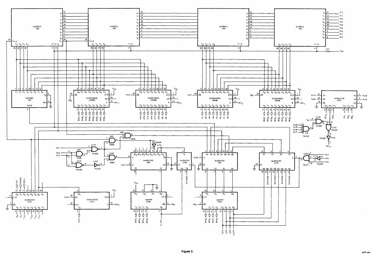
I 112 I 1,2 I 112 '0 12 PLO'0 10 10
1113 11
1311
13 11 13 PL114
1214
1214 12 14 PL2
1226
1326
1326 13 26 PL3
1328 28 28 14 28 PL4
Am2901A '4 Am2901A 1427 Am2901A 14
27 Am2901A27 15 27 PL5U34 15 U33 15 U44 15 U435
165
165 16 5 PL616
717
7'7
7 17 7 PL7176 18
618
6 18 6 PL833
18 29 33~ Cn+4 Cn Cn+4
Y3 Y2 Y1 YO F =0 F3 Y3 Y2 Y1 YO F=O Y3 Y2 Y1 YO F=O Y3 Y2 Y1 YO F=O
39 38 37 36 11 31 39 38 37 36 11 39 38 37 36 111 39 38 37 36 111 1kDVCC
PL26
PL25lB
lA
---JUo
'"---JUo
74LS04
Ul13
9 10 11 12
74LS02 ~JU113
"~Mf~:~OCL2
PL23~ 2A
PL24 ~ 2B
T9
un74LS21
PL28PL29PL30PL31
Ul35 • 1 PL3
1~Ul1213S ...;........ PL4
12 121-----PL5
1374LSll
lY
14 11 5 2
15 12 4 1
9 °3 °2 °1 °0¢~ t> CP
Am2918
DB3 ---2.Ul01
5E
3 4 7 S 13 14 17 lsi Vcc
20 _°0 °1 °2 °3 °4 °5 °6 O~U'PL27~ OE CLR
Am~~~520 CP<,.!Q..... ¢
E ~OCL2YO Y1 Y2 Y3 Y4 Y5 Y6 Y7
Am25LS2520U1ll506
Am291SUl02
°1
12J
I3 4 7 8 13 14 17118 VCC
20 DO D1 D2 D3 D4 °5 °6 °7 LJPL27~ DE CLR 1
CP<~rJ>
E ~OCL2YO Y1 Y2 Y3 Y4 Y5 Y6 Y7
US3
_ 21E '--OCL3
Am25LS2520Ulll
'~ 'z 'z'rrffzffi ffi ffi ffi ffi ffi ffi iil
20 °0PL27~ OE
I14 17
Am82S62U97
EVEN
>-
tH,I"
1 2 3 4 10 11 12 131
US3 rfoU..S:.....------------------------1r--+-+---+-----,L--------~-~------------------------.l-12-1}}.;;;,.3--t_l0 74_S_0S ---1r--, ..-+---+-------------------,
I2l--' 5 74LS04
3 ~ 74S08 Ul12 I IPL5 13 ~)O...;l-+----..... 101,111211316 65 413 41 2 3 5 6 11 101,4 13 12 91 7
:~: ---1':"2-+----1b;;- n ' ""'" :"'~ , " A "" >C, ::~:~ '" '" "~~1 Am2::S157 PL20 -2- S 1A lB 2:::
L
::
5
:B 4A 4B 4Y ::25LS15:
Y
~>o-_4__-IUl12 4 74S0S PL21--:' B U92 2G 15 15 G U125 S ~ ~ G U91 15 _ U115
~2 74LS04 2Y 1Y"::" 1A 1B -4:- ......;1T-Y__2;Y~_.;;3Yi_-..;;4;y.Y--' r G 4A 4B 3A 3B 2A 2B lA lB'\ ' "! ."" -" 'l"r r '~~ ~ ~ ~ ~
11 °0 01 D2 03 04 05 06 07
'-'~>CP
N <i: '" ~E ~ ~~
Figure 5, MPR-454

ADVANCEDMICRO
DEVICES, INC.901 Thompson Place
SunnyvaleCalifornia 94086(408) 732-2400
TWX: 910-339-9280TELEX: 34-6306
TOLL FREE(800) 538-8450