Embed Size (px)
Citation preview

ADP1043A 100 Watt Evaluation Kit
ADP1043AFB100EVALZ PRD1266
Rev. 1.3 Reference designs are as supplied ―as is‖ and without warranties of any kind, express, implied, or statutory including, but not limited to, any implied warranty of merchantability or fitness for a particular purpose. No license is granted by implication or otherwise under any patents or other intellectual property by application or use of reference designs. Information furnished by Analog Devices is believed to be accurate and reliable. However, no responsibility is assumed by Analog Devices for its use, nor for any infringements of patents or other rights of third parties that may result from its use. Analog Devices reserves the right to change devices or specifications at any time without notice. Trademarks and registered trademarks are the property of their respective owners. Reference designs are not authorized to be used in life support devices or systems.
One Technology Way, P.O. Box 9106, Norwood, MA 02062-9106, U.S.A.
Tel: 781.329.4700 Fax: 781.461.3113 ©2009 Analog Devices, Inc. All rights reserved.
FEATURES 100W Full Bridge Topology
Advanced Voltage mode Control with integrated Volt-Second Balance
I2C serial interface to PC
Software GUI
Programmable digital filters
7 PWM outputs including Auxiliary PWM
Digital Trimming
OrFET Control for Hot swap and Redundancy
Current, voltage, and temperature sense through GUI
Calibration and trimming
Analog/Digital current sharing
CAUTION This evaluation board uses high voltages and currents. Extreme caution must be taken especially on the primary side, to ensure safety for the user. It is strongly advised to power down the evaluation board when not in use. A current limited power supply is recommended as input as no fuse is present on the board.
ADP1043A EVALUATION BOARD OVERVIEW
This evaluation board features the ADP1043A in a switching power supply application. With the evaluation board and software, the ADP1043A can be interfaced to any PC running Windows 2000/XP/Vista/NT via the computer's USB port. The software allows control and monitoring of the ADP1043A internal registers. The board is set up for the ADP1043A to act as an isolated switching power supply with a rated load of 12V/8A from an input voltage ranging from a 36 to 60VDC.
EVALUATION SYSTEM CONTENTS The evaluation system package contains the following items: • Application note EVAL-ADP1043AEB (order code: ADP1043AFB100EVALZ) • ADP1043A evaluation board The USB/I2C dongle for serial communication and software CD need to be ordered separately. Order code: ADP1043A-USB-Z.
ADP1043A 100Watt PRD1266
TABLE OF CONTENTS Features ....................................................................................................................................................................................... 1
CAUTION ..................................................................................................................................................................................... 1
TOPOLOGY AND circuit description ............................................................................................................................................ 4
CONNECTORS ............................................................................................................................................................................ 4
SETTING FILES AND EEPROM .............................................................................................................................................. 6
BOARD EVALUATION ................................................................................................................................................................. 7
EQUIPMENT ............................................................................................................................................................................ 7
SETUP ...................................................................................................................................................................................... 8
ADP1043A PROGRAMMING SOFTWARE ............................................................................................................................ 10
FLAGS SETTINGS CONFIGURATIONS ................................................................................................................................ 11
GENERAL SETTINGS AND SOFTSTART ................................................................................................................................. 13
PWM AND SR SETTINGS ......................................................................................................................................................... 16
CS1 OR INPUT CURRENT SETTING ....................................................................................................................................... 17
CS2 OR OUTPUT CURRENT SETTING ................................................................................................................................... 20
LIGHT LOAD MODE ............................................................................................................................................................... 22
OUTPUT VOLTAGE SETTINGS ................................................................................................................................................ 24
DIGITAL FILTER SETTINGS AND TRANSIENT ANALYSIS ...................................................................................................... 26
ORFET SETTINGS .................................................................................................................................................................... 29
APPENDIX I – SCHEMATIC (MAIN BOARD) ............................................................................................................................ 31
APPENDIX II – SCHEMATIC (DAUGHTER CARD) ................................................................................................................... 32
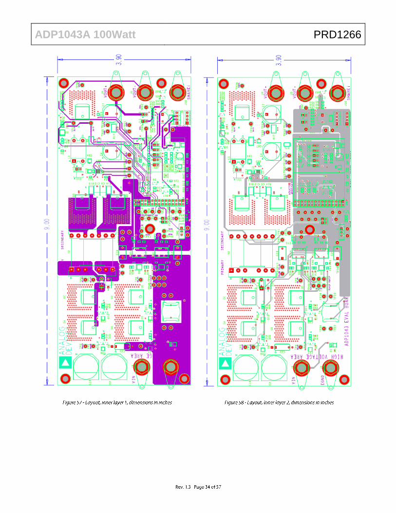
APPENDIX III – LAYOUT (MAIN BOARD) ................................................................................................................................. 33
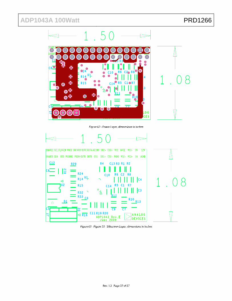
APPENDIX IV – LAYOUT (DAUGHTER CARD) ........................................................................................................................ 36
APPENDIX V - TRANSFORMER SPECIFICATION ................................................................................................................... 39
APPENDIX V - TRANSFORMER SPECIFICATION ................................................................................................................... 39
APPENDIX VI - OUTPUT INDUCTOR SPECIFICATION ........................................................................................................... 41
APPENDIX VII - THERMAL PERFORMANCE ........................................................................................................................... 42
APPENDIX VII - THERMAL PERFORMANCE ........................................................................................................................... 42
APPENDIX VIII – STEADY STATE WAVEFORMS .................................................................................................................... 43
APPENDIX IX – EFFICIENCY and VOLTAGE REGULATION ................................................................................................... 47
APPENDIX X – BILL OF MATERIALS (MAIN BOARD).............................................................................................................. 49
APPENDIX XI – BILL OF MATERIALS (DAUGHTER CARD) .................................................................................................... 52
APPENDIX XII – REGISTER FILE (ADP1043AFB100_I_0710.43R) ......................................................................................... 53
APPENDIX XIII – BOARD FILE (ADP1043AFB100_I_0710.43b) .............................................................................................. 55
APPENDIX XIV – CS1 AND CS2 MEASUREMENT vs GUI READING ..................................................................................... 56
Notes .......................................................................................................................................................................................... 57
REVISION HISTORY 07/15/2010—Revision 1.0: SPM 07/29/2010—Revision 1.1: SPM with MS feedback. 08/03/2010—Revision 1.2: SPM with MS and NSD feedback. 08/20/2010—Revision 1.3: Revisions to rev 1.2

ADP1043A 100Watt PRD1266
DEMO BOARD SPECIFICATIONS
Specification MIN TYP MAX Units Notes
VIN 36 48 60 V
VOUT 12 V
IOUT 0.0 8.0 10 A
TAMBIENT 0 30 65 ºC
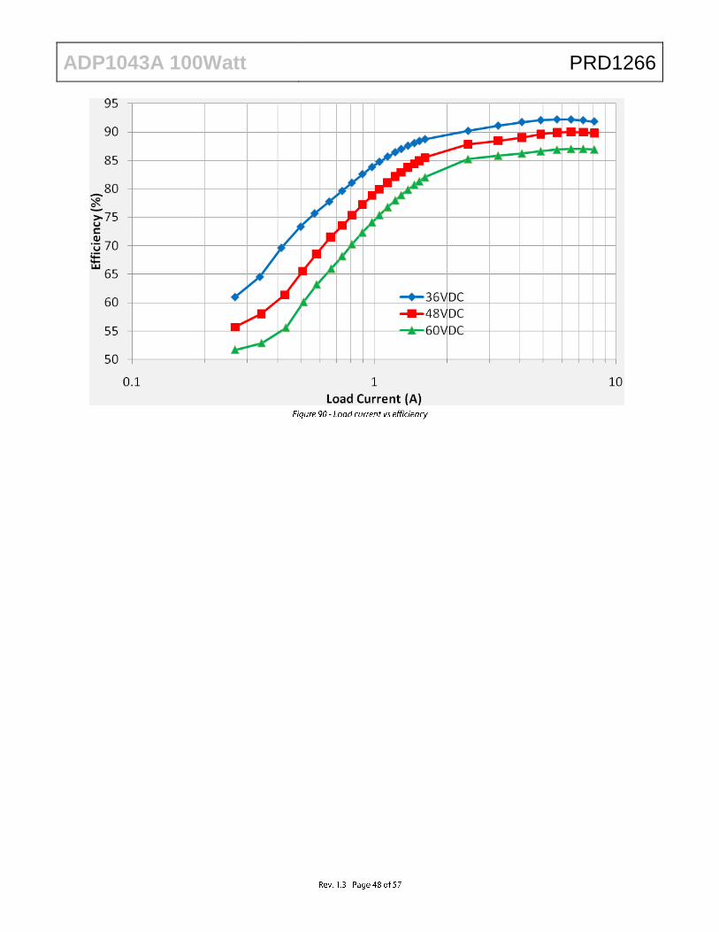
Efficiency 87.25 89.4 % Typical reading at 48V/8A load
Switching frequency 80 100.8 200 KHz
Output Voltage Ripple 1.0 V At 8A load

ADP1043A 100Watt PRD1266
TOPOLOGY AND CIRCUIT DESCRIPTION This evaluation board features the ADP1043A in a typical DC/DC switching power supply in a full bridge topology with synchronous rectification. Figure 1 gives a block diagram of the main components on the board. The circuit is designed to provide a rated load of 12V/8A from an input voltage source of 36 to 60VDC. The ADP1043A provides functions such as the output voltage regulation, over current protection, load current sharing with multiple power supplies over the share bus, over temperature protection, and power supply shutdown.
Please refer to the appendix for the detailed schematic. The primary side consists of the input terminals, full bridge switches (QA to QD), the current sense transformer (T4) and the main transformer (T2). The ADP1043A (U1, on daughter card) resides on the secondary side and is powered via the USB 5V via an ADP3303 LDO (U2, on daughter card) present on the same daughter card. The gate signal for the primary switches comes from the ADP1043A through the iCouplers ADuM5230 (U14, U16) that provide isolation and power. The output of the iCoupler is connected to a buffer as it can source only 10mA of current. This buffer (network consisting of Q5 and Q6, Q7 and Q8, Q9 and Q10, Q11 and Q12) is used to drive the full bridge switches.
The secondary side power stage consists of the synchronous rectifiers (Q2 and Q3) and their respective drivers ADP3624 (U1), output inductor (L1), output capacitor (C4, C7), sense resistor (R17), and ORFET (Q1). Diode (D2) and capacitor (C6) form a peak detector that drives the ORFET. Capacitors (C23, C64, C67) provide high frequency decoupling to lower EMI.
Diodes (D15-D18) rectify the input current signal to sense the primary current and resistor (R10) converts the current into a voltage. The over current flag trips at 1.2V. Thermistor (RT1) is placed close to the ORFET on the board allowing over temperature protection functionality to be implemented.
Also present on the secondary is the current sharing circuitry, flag LEDs (D11-D12), communications port to the software through the I2C bus.
CONNECTORS The connections to the evaluation board are shown below.
Connector Evaluation Board Function
J3 48V DC Input
J2 Ground Return for 48V DC Input
J4 12V DC Voltage Output
J5 Ground Return for 12V DC Voltage Output
J8, J9 I2C Connector
J10 Share Bus
J1 Daughter card
There is a 4 pin connector for I2C communication. This allows the software to communicate with the evaluation board through the USB port of the PC. Instead of using an auxiliary supply, the board uses the 5V input from the USB port, and generates 3.3V using an LDO for the ADP1043A. The synchronous rectifier drivers (ADP3624) are also powered by the 5V USB, but are powered from the main 12V output after the output is in regulation.
Connectors (J8 and J9) are identical and are connected in parallel to each other to allow multiple boards to be connected to the same I2C bus in a daisy chain configuration. Each board consumes between 150mA and 250mA depending on the conditions. Particular care must be taken not to overload the USB 5V rail. Some USB ports are especially those connected at a hub may shut down if overloaded, causing communication problems. In such cases an external 5V power supply is recommended to power the board between test point TP44(+) and TP21(-).
ADP1043A 100Watt PRD1266
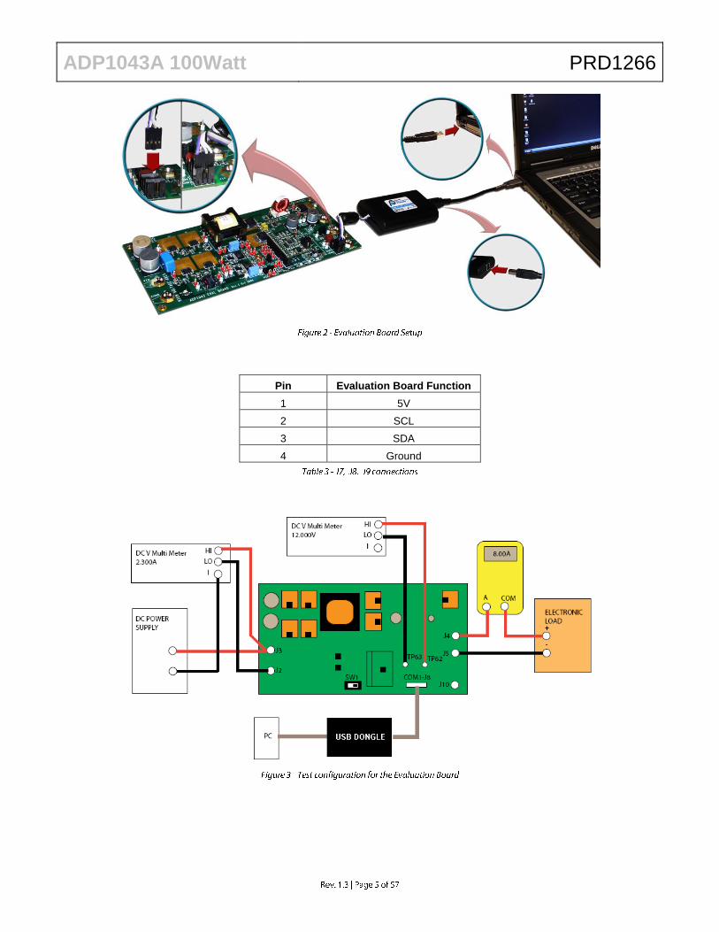
Pin Evaluation Board Function
1 5V
2 SCL
3 SDA
4 Ground

ADP1043A 100Watt PRD1266
SETTING FILES AND EEPROM The ADP1043A communicates with the GUI software using the I2C bus.
The register settings (having extension .43r) and the board settings (having extension .43b) are two files that are associated with the ADP1043A software. The register settings file contains information that govern the functionality of the part such as the over voltage and over current limits, softstart timing, PWM settings etc. The ADP1043A stores all its settings in the EEPROM. When the ADP1043A is connected to the USB dongle the LDO powers the I.C. and the GUI downloads the settings from the registers of the ADP1043A so that the state of the part is known. It is possible to save these settings in a file for later use. Older register settings are overwritten when new files are loaded.
The EEPROM on the ADP1043A does not contain any information about the board, such as current sense resistor, output inductor and capacitor values. This information is stored in board setup file (extension .43b) and is necessary for the GUI to display the correct information in the „Monitor‟ tab as well as „Filter Settings‟ window. The ADP1043A does not need this information in order to operate, but the GUI will need it in order to show the values correctly in the „Flags and Settings‟ window. The entire status of the power supply such as the ORFET and synchronous rectifiers enable/disable, primary current, output voltage and current can be thus digitally monitored and controlled using software only. Always make sure that the correct board file has been loaded for the board currently in use.
Each ADP1043A chip has trim registers for the temperature, input current and the output voltage and current. These can be configured during production and are not overwritten whenever a new register settings file is loaded. This is done in order to retain the trimming of all the ADCs for that corresponding environmental and circuit condition (component tolerances, thermal drift, etc.). A guided wizard called the „Auto Trim‟ is started which trims the above mentioned quantities so that the measurement value matches the valued displayed in the GUI to allow ease of control through software.
In the following pages it will be shown that the ADP1043A can be easily programmed to modify the behavior of the PSU under different fault and load conditions without any hardware changes. All the changes are purely through software and do not require desoldering components and replacing them with new values to specify a different operating condition

ADP1043A 100Watt PRD1266
BOARD EVALUATION
EQUIPMENT • DC Power Supply
• Electronic Load
• Oscilloscope with differential probes
• PC with ADP1043A GUI installed
• Precision Digital Multimeters (HP34401or equivalent - 6 digits) for measuring DC current and voltage

ADP1043A 100Watt PRD1266
SETUP NOTE: DO NOT CONNECT THE USB CABLE TO THE EVALUATION BOARD UNTIL THE SOFTWARE HAS FINISHED INSTALLING
1) Install the ADP1043A software by inserting the installation CD. The software setup will start automatically and a guided process will install the software as well as the USB drivers for communication of the GUI with the IC using the USB dongle.
2) Insert the daughter card in connector J1 as shown in Figure 5.
3) Ensure that the PS_ON switch (SW1 on schematic) is turned to the OFF position. It is located on the bottom left half of the board (Figure 5).
4) Connect the evaluation board to the USB port on the PC using the “USB to I2C interface” dongle as shown in Figure 2.
5) The software should report that the ADP1043A has been located on the board. Click “Finish” to proceed to the Main Software Interface Window. The serial number reported on the side of the checkbox indicates the USB dongle serial number. The windows also displays the device I2C address.
5. If the software does not detect the part it enters into simulation mode. Ensure that the connecter is connected to J8/J9 (on main board) or J7 (on daughter card). Click on „Scan for ADP1043A now‟ icon (magnifying glass) located on the top right hand corner of the screen.
5. Click on the “Load Board Settings” icon (fourth button from the left) and select the ADP1043AFB100_I_0710.43b file. This
file contains all the board information including values of shunt and voltage dividers. Note: All board setting files have an extension of .43b
ADP1043A 100Watt PRD1266
6. The IC on the evaluation board comes preprogrammed and this step is optional. The original register configuration is stored in the ADP1043AFB100_I_0710.43r register file. (I and 0710 stand for the hardware revision number and the
month/year date code respectively). Note: All register files have an extension of .43r. The file can be loaded using the second icon from the left in Figure 10.
7. Connect a DC power source (48VDC nominal, current limit to 5A) and an electronic load at the output set to 8 Amperes.
8. Connect a voltmeter on the output (connectors J4 and J5) and a differential scope probes (optional) between test points TP16 and TP17. Ensure that the differential probes are used and the ground of the probes are isolated if measurements are made on the primary and secondary side of the transformer simultaneously).
9. Turn the PS_ON switch (SW1 on schematic) to the ON position.
10. The evaluation board should now up and running, and ready for evaluation. The output should now read 12 VDC.
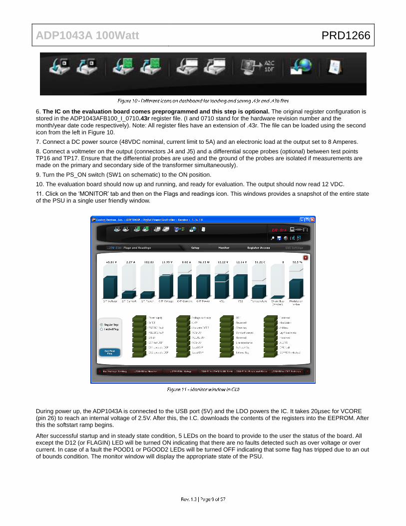
11. Click on the „MONITOR‟ tab and then on the Flags and readings icon. This windows provides a snapshot of the entire state of the PSU in a single user friendly window.
During power up, the ADP1043A is connected to the USB port (5V) and the LDO powers the IC. It takes 20µsec for VCORE (pin 26) to reach an internal voltage of 2.5V. After this, the I.C. downloads the contents of the registers into the EEPROM. After this the softstart ramp begins.
After successful startup and in steady state condition, 5 LEDs on the board to provide to the user the status of the board. All except the D12 (or FLAGIN) LED will be turned ON indicating that there are no faults detected such as over voltage or over current. In case of a fault the POOD1 or PGOOD2 LEDs will be turned OFF indicating that some flag has tripped due to an out of bounds condition. The monitor window will display the appropriate state of the PSU.

ADP1043A 100Watt PRD1266
LED Location Description
D1 (Red) Bottom left Indicates input voltage is present
D10 (Yellow) Bottom right PGOOD1 signal (active low)
D11 (Red) Bottom right PGOOD2 signal (active low)
D12 (Red) Bottom right FLAGIN signal
D13 (Red) Top right Indicates ORFET is turned ON
ADP1043A PROGRAMMING SOFTWARE The goal of this evaluation kit is to allow the user to get an insight into the flexibility offered by the extensive programming options offered by the ADP1043A. Several test points on the board allow easy monitoring of the various signals. The user can also use the software to program multiple responses (such as disable power supply or turn off ORFET) for various fault conditions.
The following sections give provide a good overview of the software as well as the test data experiments that the user might typically evaluate. There are 9 main windows (blue icons in figure below) where the user can use to program and evaluate the PSU. They can be accessed from the Setup window in the GUI.

ADP1043A 100Watt PRD1266
FLAGS SETTINGS CONFIGURATIONS
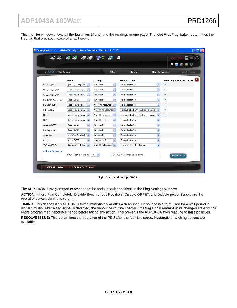
The following state machine diagram provides a graphical idea as to how the flags in the ADP1043A operate and hence gain insight into the working of the IC.
Basically when a flag is triggered, the controller waits for a programmable debounce time before taking any action. The response to each flag can be programmed individually. The flags can be programmed in a single window by hitting the FLAG SETTINGS icon in the MONITOR tab in the GUI and the state of the power supply can be monitored by clicking on the FLAGS AND READINGS icon in the MONITOR tab.
ADP1043A 100Watt PRD1266
This monitor window shows all the fault flags (if any) and the readings in one page. The „Get First Flag‟ button determines the first flag that was set in case of a fault event.
The ADP1043A is programmed to respond to the various fault conditions in the Flag Settings Window.
ACTION: Ignore Flag Completely, Disable Synchronous Rectifiers, Disable ORFET, and Disable power Supply are the
operations available in this column.
TIMING: This defines if an ACTION is taken immediately or after a debounce. Debounce is a term used for a wait period in
digital circuitry. After a flag signal is detected, the debounce routine checks if the flag signal remains in its changed state for the entire programmed debounce period before taking any action. This prevents the ADP1043A from reacting to false positives.
RESOLVE ISSUE: This determines the operation of the PSU after the fault is cleared. Hysteretic or latching options are
available.
ADP1043A 100Watt PRD1266
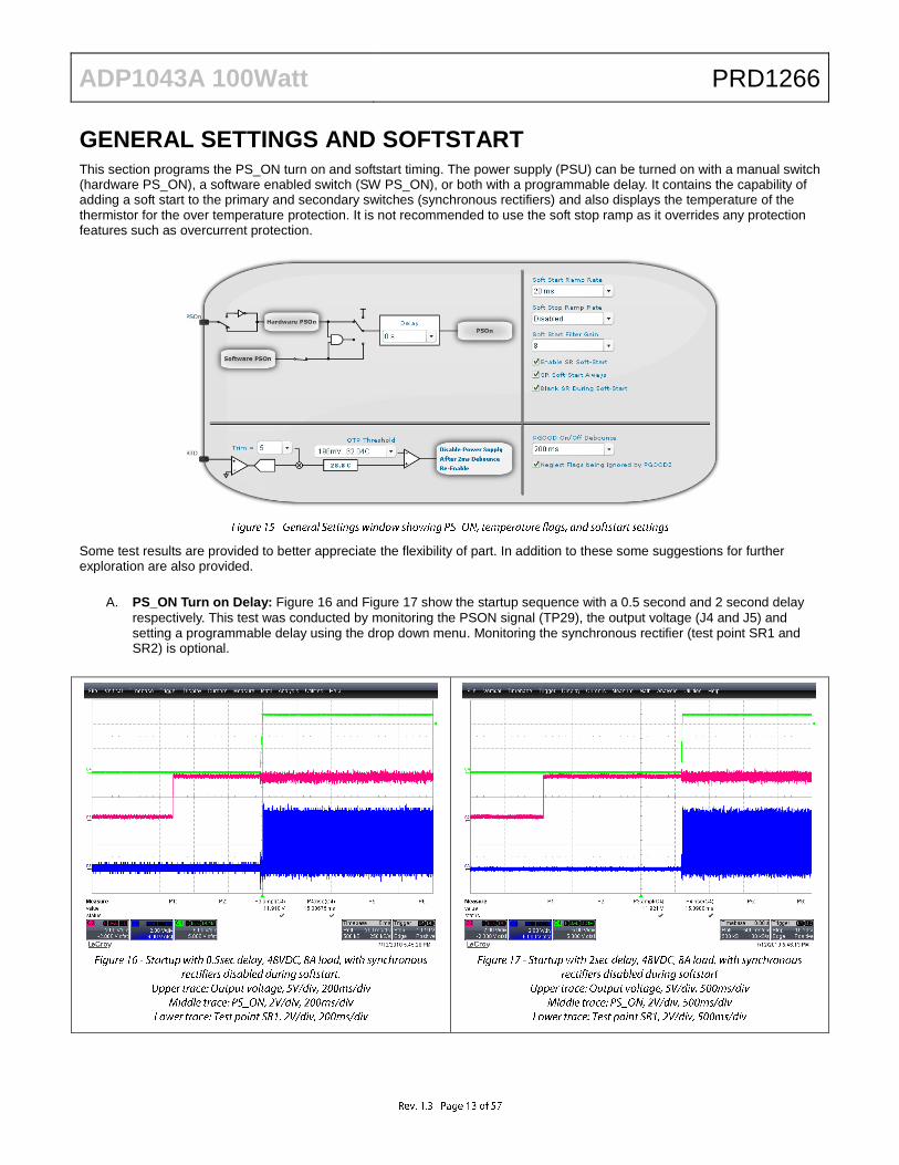
GENERAL SETTINGS AND SOFTSTART This section programs the PS_ON turn on and softstart timing. The power supply (PSU) can be turned on with a manual switch (hardware PS_ON), a software enabled switch (SW PS_ON), or both with a programmable delay. It contains the capability of adding a soft start to the primary and secondary switches (synchronous rectifiers) and also displays the temperature of the thermistor for the over temperature protection. It is not recommended to use the soft stop ramp as it overrides any protection features such as overcurrent protection.
Some test results are provided to better appreciate the flexibility of part. In addition to these some suggestions for further exploration are also provided.
A. PS_ON Turn on Delay: Figure 16 and Figure 17 show the startup sequence with a 0.5 second and 2 second delay
respectively. This test was conducted by monitoring the PSON signal (TP29), the output voltage (J4 and J5) and setting a programmable delay using the drop down menu. Monitoring the synchronous rectifier (test point SR1 and SR2) is optional.

ADP1043A 100Watt PRD1266
B. Softstart ramp and SR blanking: Figure 18 and Figure 19 show the startup sequence with the synchronous
rectifiers enabled/disabled with a 20ms and 40ms softstart ramp respectively.
This test was conducted by monitoring the output voltage (J4 and J5) and the test points SR1/SR2 during a startup condition. The „Blank SR during softstart check box and the „Softstart ramp rate‟ dropdown menu were appropriately selected.
C. SR enable during softstart: Figure 20 shows the startup sequence with the synchronous rectifiers enabled during
softstart. This test was conducted by monitoring the output voltage (J4 and J5) and the synchronous rectifier test points test points (SR1, SR2) during a startup condition. The „Blank SR during softstart check box was left unchecked.

ADP1043A 100Watt PRD1266
D. SR softstart: This test shows the capability of the softstart ramp or fade in sequence applied to the synchronous
rectifiers. The „Enable SR softstart‟ button was checked. Figure 21 and Figure 22 show a zoomed in snapshot of the duty cycle at the beginning and end of the softstart ramp
Additional things to try:
a) Implementation of different softstart timings in combination with different PS_ON delays.
b) Disabling „Soft Start Always‟ and evaluating the performance after a fault like UVP/OVP disables the PSU.
c) Trimming the RTD register by measuring the temperature at the OrFET and changing the trim setting.
d) Disable the OrFET allowing its body diode to conduct the output current. Then set different OTP thresholds.
e) Enable Softstart always and see the PSU start a softstart ramp everytime a fault such as a temporary short circuit.

ADP1043A 100Watt PRD1266
PWM AND SR SETTINGS The switches on the primary and the synchronous rectifier timings are controlled in this window. This window programs the switching frequency, timings of the synchronous rectifier, the type of modulating edge (rising or falling), modulation type (positive or negative). The IC can be programmed to run at a fixed duty cycle.
The Pulse Skipping mode is activated when the controller requires a duty cycle less than the „modulation low limit‟ to maintain output regulation.
Note 1: All the signals shown below represent the gate drive signals at the output pins of the IC. Note 2: Although the switching frequency can be increased, the software does not account for the dead times and these have to be programmed manually by measuring the propagation delays between the output of the ADP1043A and the gate of the MOSFET. A 200nsec delay is conservative for the evaluation board.
Things to try:
a) Referring to the schematic, turning on QA and QB for the entire period of Ts/2 (with appropriate deadtimes) and modulating only the bottom MOSFETs.
b) Enabling/Disabling Pulse skipping mode and measuring standby power (by disabling the LEDs on the board additional power can be saved).
c) Doubling the switching frequency (see accompanying file 200KHz with VS balance.43r) Note: The board is designed to operate at switching frequencies of up to 200kHz with air flow cooling (i.e. a fan). Beyond that, frequency damage to the FETs may occur.
d) Programming an imbalance in the ON times of the MOSFETs of each branch and evaluating Volt-Second balance.
e) Measuring the effect on standby power by reducing the „Modulation Low Limit‟ with/without pulse skipping.
f) Run the software in simulation mode and program the PWM settings for a different topology.

ADP1043A 100Watt PRD1266
CS1 OR INPUT CURRENT SETTING The input current settings are accessed using the CS1 Settings block. It is used to program the fast and accurate ADCs for pulse by pulse current limiting, leading edge blanking, and enable the volt-sec balance correction to the bottom MOSFETs of the full bridge converter and/or the synchronous rectifiers.
Some tests are provided to better appreciate the flexibility of part. In addition to these, some suggestions for further evaluation are also provided.
A. CS1 Accurate OCP: Figure 25 shows the CS1 accurate OCP flag and a reenable after 1 second
This test was conducted by setting the CS1 accurate OCP limit of 2.76A (drop down menu in the GUI) which is lower than the current at minimum voltage. Then the input voltage was ramped down from 60V until the OCP limit was triggered. . Monitoring the PWM signal at test point OUTA clearly shows the shutdown of the PWM.

ADP1043A 100Watt PRD1266
B. Volt Second Balance feature: The CS1 settings window has the volt second feature that measures the average
current in each leg of the full bridge topology. The algorithm reduces (or increases) the conduction time of each branch by varying the pulse width of the MOSFET gate signals applied to OUTB and OUTD depending if there was an increase (or decrease) of current in the corresponding branch. A maximum of 80nsec can be accounted for by this algorithm.
This test was conducted by purposely introducing a mismatch of 75nsec in the PWM settings window. This mismatch clearly shows that the transformer is close to saturation on one end. Figure 27 shows the imbalance and Figure 28 shows the corrected imbalance after the feature was turned on in the GUI by closing the switch. The primary current can be measured using a current probe and by using a small loop of wire in place of jumper L3 or C10 on the board.
ADP1043A 100Watt PRD1266
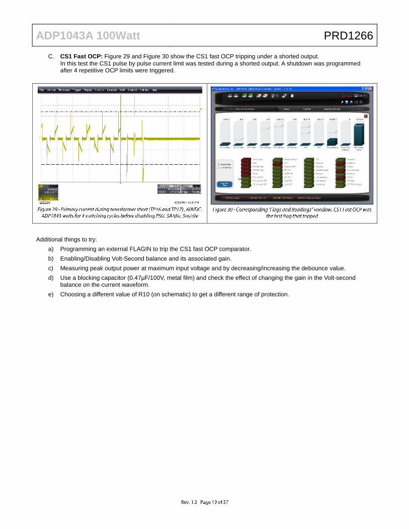
C. CS1 Fast OCP: Figure 29 and Figure 30 show the CS1 fast OCP tripping under a shorted output.
In this test the CS1 pulse by pulse current limit was tested during a shorted output. A shutdown was programmed after 4 repetitive OCP limits were triggered.
Additional things to try:
a) Programming an external FLAGIN to trip the CS1 fast OCP comparator.
b) Enabling/Disabling Volt-Second balance and its associated gain.
c) Measuring peak output power at maximum input voltage and by decreasing/increasing the debounce value.
d) Use a blocking capacitor (0.47µF/100V, metal film) and check the effect of changing the gain in the Volt-second balance on the current waveform.
e) Choosing a different value of R10 (on schematic) to get a different range of protection.

ADP1043A 100Watt PRD1266
CS2 OR OUTPUT CURRENT SETTING The output current settings window is accessed using the CS2 Settings block. This window also features trimming registers , line impedance feature, threshold for over current protection (OCP), the light load threshold, and constant current mode.
The following waveforms display some of the features that can be programmed using this window.
A. Over Current Protection (OCP): Figure 32 and Figure 33 show hysteretic and latching OCP respectively.
An over current condition can be easily created by shorting the load or increasing the output current beyond the OCP limt. Different reactions to the fault can be programmed by either re-enabling the PSU after 1 second or a complete shutdown through the drop down menus in the GUI.

ADP1043A 100Watt PRD1266
B. Constant Current Mode: Figure 34 shows the output voltage ramping down linearly by 60% during constant current
mode.
Closing the switch on the trace connected to the Constant Current Block enables CC mode. In this the output voltage linearly drops by 60% of its nominal value when the load current reaches 90% of the OCP limit. In this example, the IC enters CC mode when the load was set to 9.5A which is 94.7% of the OCP limit and output voltage drops to 7 Volts in during CC.
Additional things to try:
a) Setting a different light load thresholds and measuring its effect on efficiency
b) Using the line impedance feature to simulate the voltage drop through a 2 foot output cable.
c) Reducing the current sense resistor value (R17) and changing the range of the full scale voltage drop on CS2+ and CS2-
d) Increasing the debounce time on CS2 OCP limit and measuring the peak output power during a short circuit test.
e) Setting different OCP limits and setting a different response such as disable SyncRec

ADP1043A 100Watt PRD1266
LIGHT LOAD MODE The ADP1043A can be programmed to optimize performance when the output current drops below a certain level. The light load threshold is set in a manner to reduce the losses in the synchronous rectifiers to enter into DCM and reduce the power loss in the SR drivers and increase efficiency. A hysteresis is provided on this threshold to avoid oscillations.
When operating in light load mode the corresponding flag will be set as well as the SR off flag as shown in the monitor window (Synchronous rectifiers turned red in figure below), and the light load filter settings will be used. Using this in combination with Pulse Skipping aids in reducing standby power consumption. The ACSNS flag is used to sense the voltage at the front side of the inductor connected to the transformer (T2).

ADP1043A 100Watt PRD1266
ADP1043A 100Watt PRD1266
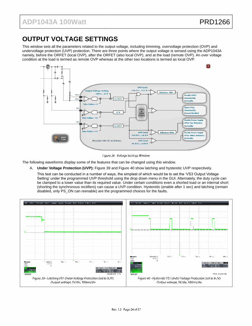
OUTPUT VOLTAGE SETTINGS
This window sets all the parameters related to the output voltage, including trimming, overvoltage protection (OVP) and undervoltage protection (UVP) protection. There are three points where the output voltage is sensed using the ADP1043A namely, before the ORFET (local OVP), after the ORFET (also local OVP), and at the load (remote OVP). An over voltage condition at the load is termed as remote OVP whereas at the other two locations is termed as local OVP.
The following waveforms display some of the features that can be changed using this window.
A. Under Voltage Protection (UVP): Figure 39 and Figure 40 show latching and hysteretic UVP respectively.
This test can be conducted in a number of ways, the simplest of which would be to set the „VS3 Output Voltage Setting‟ under the programmed UVP threshold using the drop down menu in the GUI. Alternately, the duty cycle can be clamped to a lower value than its required value. Under certain conditions even a shorted load or an internal short (shorting the synchronous rectifiers) can cause a UVP condition. Hysteretic (enable after 1 sec) and latching (remain disabled, only PS_ON can reenable) are the programmed choices for the faults.
ADP1043A 100Watt PRD1266
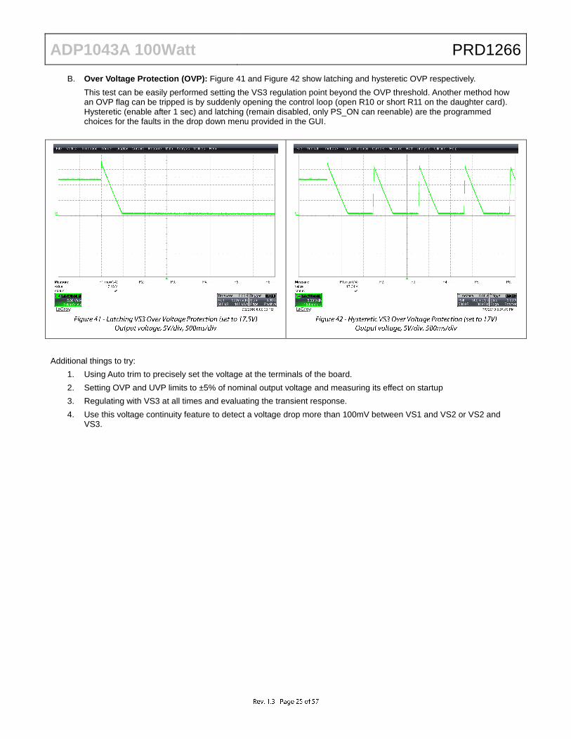
B. Over Voltage Protection (OVP): Figure 41 and Figure 42 show latching and hysteretic OVP respectively.
This test can be easily performed setting the VS3 regulation point beyond the OVP threshold. Another method how an OVP flag can be tripped is by suddenly opening the control loop (open R10 or short R11 on the daughter card). Hysteretic (enable after 1 sec) and latching (remain disabled, only PS_ON can reenable) are the programmed choices for the faults in the drop down menu provided in the GUI.
Additional things to try:
1. Using Auto trim to precisely set the voltage at the terminals of the board.
2. Setting OVP and UVP limits to ±5% of nominal output voltage and measuring its effect on startup
3. Regulating with VS3 at all times and evaluating the transient response.
4. Use this voltage continuity feature to detect a voltage drop more than 100mV between VS1 and VS2 or VS2 and VS3.
ADP1043A 100Watt PRD1266
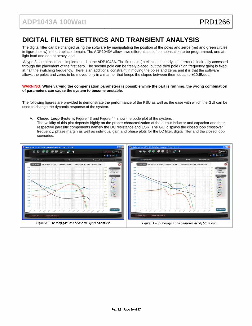
DIGITAL FILTER SETTINGS AND TRANSIENT ANALYSIS The digital filter can be changed using the software by manipulating the position of the poles and zeros (red and green circles in figure below) in the Laplace domain. The ADP1043A allows two different sets of compensation to be programmed, one at light load and one at heavy load.
A type 3 compensation is implemented in the ADP1043A. The first pole (to eliminate steady state error) is indirectly accessed through the placement of the first zero. The second pole can be freely placed, but the third pole (high frequency gain) is fixed at half the switching frequency. There is an additional constraint in moving the poles and zeros and it is that the software allows the poles and zeros to be moved only in a manner that keeps the slopes between them equal to ±20dB/dec.
WARNING: While varying the compensation parameters is possible while the part is running, the wrong combination of parameters can cause the system to become unstable.
The following figures are provided to demonstrate the performance of the PSU as well as the ease with which the GUI can be used to change the dynamic response of the system.
A. Closed Loop System: Figure 43 and Figure 44 show the bode plot of the system.
The validity of this plot depends highly on the proper characterization of the output inductor and capacitor and their respective parasitic components namely the DC resistance and ESR. The GUI displays the closed loop crossover frequency, phase margin as well as individual gain and phase plots for the LC filter, digital filter and the closed loop scenarios.

ADP1043A 100Watt PRD1266
B. Transient Response for load step: Figure 45 and Figure 46 show the transient response at 36 and 60VDC
respectively.
A dynamic load from 1-8A (slew rate 1A/µs) at a frequency of 20-25Hz can be set up to conduct this test. The output voltage must be measured at the connectors J4 and J5 with very small loop area between the positive and negative of the probes to minimize noise.
C. Transient Response under DCM/CCM transition: Figure 47 shows the dynamic response of the system under a
load step of 0.2-5A (slew rate1A/µs). A low starting current is chosen so that the converter is forced to disable the synchronous rectifiers due to the light load threshold setting in the CS2 window. In contrast, Figure 48 shows the response with the light load threshold set at 0A (SR always on). This forces the output inductor current to be continuous and the converter remains in CCM despite the load condition drawing energy from the output capacitor to charge the inductor.

ADP1043A 100Watt PRD1266
Additional things to try:
a) Tweaking the light load transient response (0-500mA step load).
b) Increasing the crossover frequency and measure transient response
c) Measuring transient response under different load steps
d) Increasing the phase margin to 60 degrees by cancelling the double pole of the output LC filter by the two zeros of the Type 3 compensation.
e) Measuring the transient response (0.2A - 8A) by enabling the light load mode at 0.0A (SR always enabled) thus keeping the output inductor in CCM regardless of the load.
f) Measuring the dynamic response at 200KHz switching frequency.

ADP1043A 100Watt PRD1266
ORFET SETTINGS The ADP1043A includes features such as hot swapping as well as protection against a reverse current from other PSUs connected on the same bus with the use of active ORing (ORFET). This window sets the turn on condition of the OrFET depending upon the voltage threshold across it as well as its turn off depending upon the reverse current flowing in the current sense resistor CS2
- - CS2
+. This enables hot swapping and allows additional PSUs to be connected to the same bus without
any interruption with sufficient protection.
The following waveforms display some of the features that can be changed using this window.
A. Load OVP action on OrFET: Figure 50 shows the OrFET being disabled when a bus voltage is greater than the local
voltage. A DC power supply can be connected to the output terminals of the board (J4, J5). Care should be taken to ensure that the output voltage is not beyond the voltage rating of the output capacitor (C7) and the absolute maximum VCC rating of the SR driver (U1). Here the load OVP flag is used to protect the PSU by disabling the OrFET. The body diode of the MOSFET (Q1) is reversed biased during this condition.
ADP1043A 100Watt PRD1266
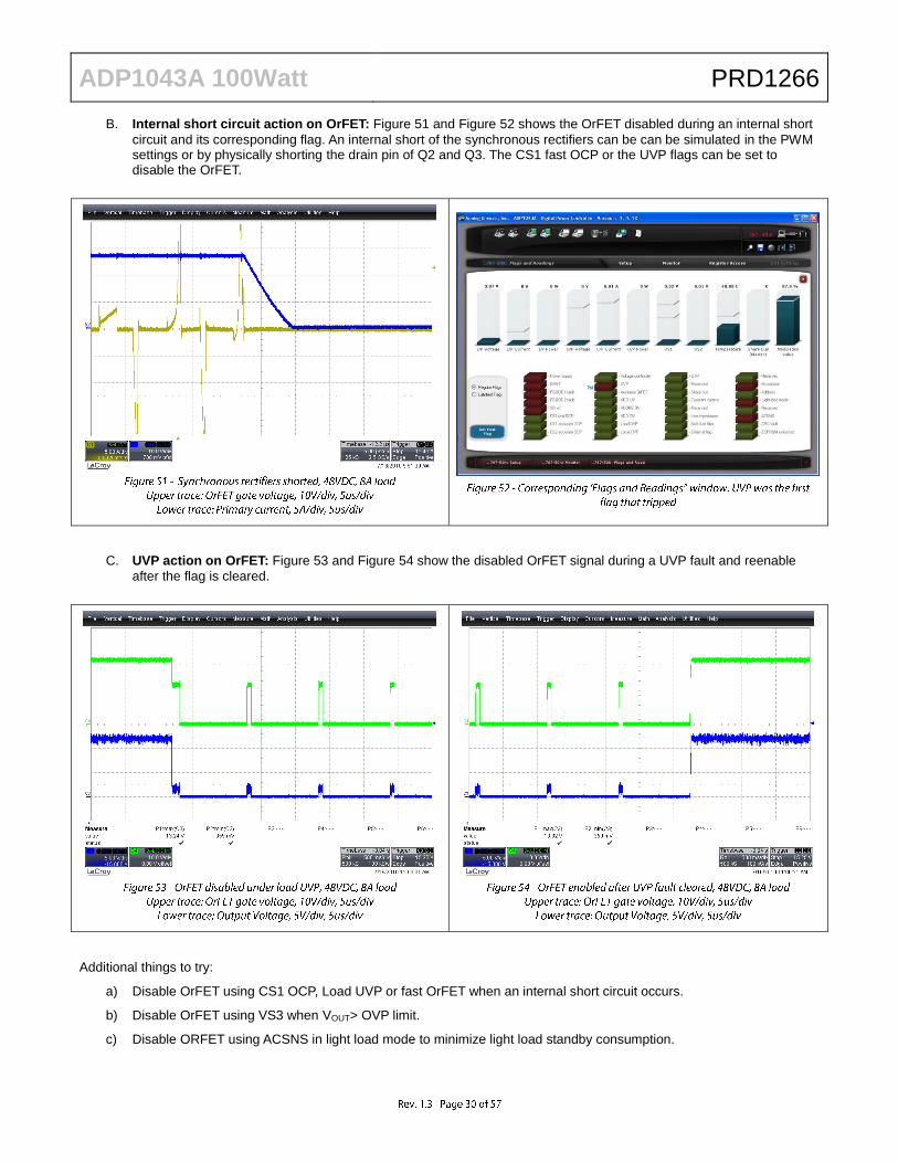
B. Internal short circuit action on OrFET: Figure 51 and Figure 52 shows the OrFET disabled during an internal short
circuit and its corresponding flag. An internal short of the synchronous rectifiers can be can be simulated in the PWM settings or by physically shorting the drain pin of Q2 and Q3. The CS1 fast OCP or the UVP flags can be set to disable the OrFET.
C. UVP action on OrFET: Figure 53 and Figure 54 show the disabled OrFET signal during a UVP fault and reenable
after the flag is cleared.
Additional things to try:
a) Disable OrFET using CS1 OCP, Load UVP or fast OrFET when an internal short circuit occurs.
b) Disable OrFET using VS3 when VOUT> OVP limit.
c) Disable ORFET using ACSNS in light load mode to minimize light load standby consumption.

ADP1043A 100Watt PRD1266
APPENDIX I – SCHEMATIC (MAIN BOARD)
+
C2330uF
1 2
TP
19
R5
8
15K
Hi Current
12V
R2
5D
NI
R7
02
.2K
F1
1A
12
R2
0D
NI
QA
FD
D3
67
2
2
1
3
D1
6B
AV
70
13
2
75V
82A
R1
9D
NI
R1
80
OU
TB
TP
25
Q4
FM
MT
48
9
3 1
2
TP
14
TP
52
R1
14
.7
R2
310K
QC
LO
+
C1
31
0U
F
12
25V
VS
3-
C4
3D
NI
1A
Q1
IRF
28
07
S
2
1
3
100V
12V
EN
D3
SM
Z1
6
21
D9
DN
I
13
2
ELECT ALUM
T4
5 6
1 2 4 3
TP
35
OU
TC
25V
D1
9B
AV
70
13
2
Q2
IRF
28
07
S
2
1
3
R1
413
R5
0
10K
TP
22
C5
2700pF
TP
5
R9
4.7
25V
C1
0JU
MP
ER
D7
SS
2H
10
21
VS
3-
TP
2
Q3
IRF
28
07
S
2
1
3
t
RT
1N
TC
+C
11
DN
I
1 2
L1
10
uH
10
A
13
24
OU
TD
TP
38
C2
6D
NI
C6
710uF
TP
64
R3
24
.9k
D6
SS
2H
10
21
TP
23
TP
61
C6
8D
NI
+3
.3V
PG
ND
R5
JU
MP
ER
34
12
TP
48
TP
39
C62 10nF
Q1-G
C1
61000pF
TP
15
TP
20
QC
FD
D3
67
2
2
1
3
C63 10nF
+3
.3V
R1
70
.01
Oh
m
34
12
T2
12 3 46
78 910
5
11
12
13
QB
HI
TP
7
T2-H
I
100V
TP
45
OT
W
PG
ND
100V
44A
100V
44A
R5
1
10K
25V
C6
910nF
GA
TE
R7
910
R7
10
AG
ND
PG
ND
TP
30
AG
ND
TP
60
CS
I
16V
1W
C4
610nF
YE
LL
OW
TP
29
T2-L
O
R5
50
100V
R4
470
C2
2100nF
1W
C7
10
.47
uF
TP
11
SL
C
D15BAV7013
2
SR
2
25V
1A
D1
0LE
D
2 1
TP
6
TP
17
C1
22700pF
J1
6
12
SD
A
OTW
TP
49
R7
610K
R5
60
L3
JU
MP
ER
12
D2
BA
V70
13
2
SR
1
1A
75V
82A
+5
V
TP
21
GR
EE
N
25V
C2
40
.1U
F
+C
36
10
UF
1 2
+3
.3V
TP
33
TP
13
25V
C2
00
.01
5U
F
PG
ND
R7
710K
D1
LE
D
2 1
Q13
FM
MT
48
9
3 1
2R
57
10K
OTW
C7
00
.47
uF
U1
AD
P3
62
4A
EN
1IN
A2
3PGND
INB
45O
UT
B
6VCC
7O
UT
A
OTW
8
HIGH VOLTAGE AREA
J1
51
2
AS
CN
S
R5
2
10K
100V
25V
1A
C6
1uF
+5
V
Q2
PG
ND
RE
D
1W
D8
BA
V70
1 3
2
J1
31
2
TP
46
R4
61
C7
20
.47
uF
VS
3+
OU
TA
UX
D1
8B
AV
70
13
2
TP
27
25V
1A
C1
8D
NI
Q3
R6
61K
+C14
330uF
1 2
TP
36
TP
10 O
UT
B
R1
513
C9
DN
I
R6
22
.2K
C3
433pF
12V
TP
9
C3
533pF
R6
32
.2K
TP
12
C3
733pF
R6
0
100
+C
17
22
UF
1 2
25V C3
333pF
+C
23
4.7
uF
1 2
CS
2-
25V
1A
+3
.3V
100V
SC
L
SD
A
R6
1
100
VS
3+
iCOUPLER
D4
BA
V701
3
2
TP
37
C3
2390pF
D2
1B
AV
70 1
3
2
25V
C6
410uF
+3
.3V
R4
71k
25V
1A
CS
2+
C2
1D
NI
TP
26
J1
8
12
J1
2 JUMPER
Drive
J1
9
12
R2
42
.2K
TP
8
75V
82A
25V
1A
VS
3-
D5
MB
RS
11
00
T32
1
100V
1A
+5
V
C3
80
.47
uF
AD
10
43
DA
UG
HT
ER
CA
RD
R53 2.2K
U1
4A
Du
m5
23
0
2
VDD1
GN
DB
11
VD
DB
10
GN
D2
8
VO
B9
VIS
O15
GN
Dis
o14
VO
A16
7 VDD2
3V
AD
J
VIA
5
VIB
6
GN
D1
GN
D1
4
NC
12
NC
113
Q5
FM
MT
48
92
3 1
Q6
FM
MT
58
9 31
2+
C2
81
UF
1 2
+3
.3V
C4
533pF
+3
.3V
R8
0
100
C4
933pF
25V
R3
58
.06
k
+C
27
4.7
UF
1 2
R3
62
.05
k
R6
8470
Q7
FM
MT
48
92
3 1
Q8
FM
MT
58
9 31
2
R3
210
-+
U7
AO
P297
3 21
8 4
12V
TP
47
25V
1A
+
C3
91
0U
F
1 2
J4
VO
UT
+
1
QD
HI
PS
ON
16V
+3
.3V
J5
VO
UT
-
1
TP
43
16V
+C
41500uF
1 2
C25DNI
RE
D
TP
3
TP
34
GND ISOLATED
+C
71500uF
1 2
SW
1
21 3
R7
210
C4
4100nF
PL
AG
IN
TP
16
25V
R4
84
.7M
2A
25V
J3
VIN
1
R5
42
.2K
TP
40
J1
CO
NN
RE
CE
PT 3
0P
OS
ACSNS16
SR
218
30NC
PGND21
CS2-19
CS2+20
SR
117
CS
115
RT
D5
VS122
GATE24
VS223
VS
3+
25
VS
3-
26
VD
D28
AG
ND
29
SD
A3
SC
L4
OU
TD
11
OUTB13
OU
TC
12
OUTA14
PGOOD18
PGOOD27
FLAGIN6
+5V27
OUTAUX10
PSON9
SHAREo1
SHAREi2
SD
A
TP
63
D1
1LE
D
2 1
R6
71K
J1
4
12
VS
3-
QC
HI
12V
QA
HI
J2
0
12
D1
2LE
D
2 1
100V
2A
VS
3+
QB
FD
D3
67
2
2
1
3
iCOUPLERQ
DF
DD
36
72
2
1
3
D1
3
LE
D21
J10
I S
HA
RE
1
AG
ND
SC
L
R1
30
TP
1
TP
31
RE
D
C3
100nF
+C
15
10
UF
1 2
25V
100V
44A
D2
0B
AW
56
31
2
D1
4D
NI
13
2
R6
4100
QA
LO
D2
2B
AW
56
31
2
R3
71
Q1-S
TP
41
J2
EG
ND
1
TP
42
R7
310
TP
18
+5
V
C4
00
.47
uF
U1
5A
Du
m5
23
0
2
VDD1
GN
DB
11
VD
DB
10
GN
D2
8
VO
B9
VIS
O15
GN
Dis
o14
VO
A16
7 VDD2
3V
AD
J
VIA
5
VIB
6
GN
D1
GN
D1
4
NC
12
NC
113
TP
62
Q9
FM
MT
48
92
3 1
R1
010
Q10
FM
MT
58
9 31
2
GND ISOLATED
C1
9
0.0
15
UF
+C
29
1U
F
1 2
R3
810
R3
910
R4
08
.06
k
R4
110K
+C
30
4.7
UF
1 2
R4
22
.05
k
C4
10
.47
uF
Q11
FM
MT
48
92
3 1
J8
CO
M1
12 3 4
Q12
FM
MT
58
9 31
2
C3
1D
NI
100V
44A
R4
310
R4
410
VS
3+
R4
510K
TP
50
R5
9100K
+
C4
21
0U
F
1 2
PG
ND
Q1-D
R4
910K
R7
410K
R7
510
G-E
AR
TH
R8
110
J1
1
JUMPER
TP
4
C8
1U
F
J1
7
12
100V
2A
R7
81K
+3
.3V
SP
M68280
R1
60
OU
TA
TP
51
25V
1A
D17BAV7013
2
100V
R3
41
+5V
TP
44
J9
CO
M2
12 3 4
PG
ND

ADP1043A 100Watt PRD1266
APPENDIX II – SCHEMATIC (DAUGHTER CARD)
+12V
C5
1.0
uF
CS
1
CS
2-
R24
2.2
k
OU
TD
SH
AR
Ei
AD
P3
30
3
FLA
GIN
OU
TA
RTD
R29
2.2
k
SR
1
R151.2k
PG
OO
D1
2
110k
SH
AR
E0
VS
3+
+3.3
V
+3.3
V
C16
DN
I
CS
2+
R17
0
R4
DN
I
GA
TE
C7
DN
I
SR1
R14
1.2
k
U1
AD
P1
04
3
1 2 3 4 5 6 7 8
9
10
11
12
15
13
14
16
17
18
19
20
21
22
23
24
25
26
27
28
29
30
31
32
PAD
VS
2
AG
ND
VS
1
CS
2-
CS
2+
AC
SN
S
CS
1
PG
ND
SR1
SR2
OUTA
OUTB
OUTAUX
OUTC
OUTD
GATE
SC
L
SD
A
PS
ON
FLA
GIN
PG
OO
D2
PG
OO
D1
SH
AR
EO
SH
AR
EI
DGND
VCORE
VDD
RTD
ADD
RES
VS3-
VS3+
33
PG
ND
C10
DN
I
SD
A
R7
11k
R3
10k
+3.3
V
OUTB
C9
DN
I
C13
OUTAUX
2
SD
A
DN
I
AC
SN
S
OU
TC
C16
J1
12345678910
11
12
13
14
15
16
17
18
19
20
21
22
23
24
25
26
27
28
29
30
NOTES:
VS
1
SD
A
CS
1
FLA
GIN
PG
OO
D2
PS
ON
J7
1 2 3 4
C17
+3.3
V
SR
2
VS
1
DN
I
VS
3-
+5V
UN
LE
SS
OTH
ER
WIS
E S
PE
CIF
IED
.
33pF
VS
3+
SR2
1:
R3,
R4,
R5,
R6,
R7,
R8,
R10,
R11 A
RE
0.1
% 2
5ppm
33pF
OUTC
GATE
DG
ND
+5V
R8
1k
R13
0
R33
DN
I
R11
1k
Low
Sid
e
SC
L
R16
0
R4
10k
R32DNI
R5
11k
PS
ON
Hig
h S
ide
SH
AR
E0
C3
DN
I
OU
TB
R1
27K
R6
1k
C2
DN
I
R12
1
SC
L
D2
1N
4148
2 1
C14
0.1
uF
CS
2+
AC
SN
S
AG
ND
C4
DN
IR10
11k
C1
DN
I
C17
DN
I
VS
2
PG
OO
D2
C60.1uF
+12V
C13
100pF
R192.2k
10k
OU
TA
UX
D1
1N
4148
2 1
C10
100pF
2
PG
OO
D1
CS
2-
C8
0.1
uF
C15
1000pF
VS
2
C12
0.4
7uF
R2049.9k
110k
C11
0.1
uF
DN
I
RTD
50V
U2
1 2 3 45678
OU
T1
OU
T2
NR
GN
DS
D
ER
R
IN2
IN1
+5V
R3
VS
3-
+3.3
V
R2
1k
OUTA
OUTD
SC
L
10k
SH
AR
Ei
DN
I

ADP1043A 100Watt PRD1266
APPENDIX III – LAYOUT (MAIN BOARD)
ADP1043A 100Watt PRD1266

ADP1043A 100Watt PRD1266

ADP1043A 100Watt PRD1266
APPENDIX IV – LAYOUT (DAUGHTER CARD)
ADP1043A 100Watt PRD1266

ADP1043A 100Watt PRD1266

ADP1043A 100Watt PRD1266
APPENDIX V - TRANSFORMER SPECIFICATION
PARAMETER MIN TYP MAX UNITS NOTES
Core and Bobbin ETD 29 Horizontal, 3F3 or equivalent
Primary inductance 77 µH Pins 2,3 to pin 4,5
Leakage inductance 2.31 3 µH Pins 2,3 to pin 4,5 with all other windings shorted
Magnetizing current 1.58 A
Resonant frequency 850 KHz Pins 2,3 to pin 4,5 with all other windings open
Table 5 - Transformer specifications
PARAMETER MIN TYP MAX UNITS NOTES
Core 0077720A7, KoolMu, Magnetics Inc.
Pearmeability (µo) 75
Inductance 6.5 10 µH
DC resistance 6 mΩ
2, 3
11
10
9
4, 5
6T, Copper foil, 4 mil, 0.6inch
wide
3T, Copper foil, 4 mil, 0.6inch
wide
3T, Copper foil, 4 mil, 0.6inch
wide
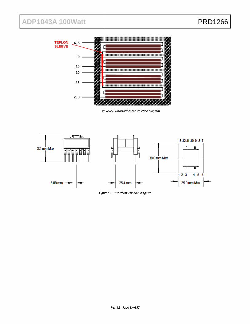
ADP1043A 100Watt PRD1266
2, 3
11
10
10
9
4, 5 TEFLON SLEEVE

ADP1043A 100Watt PRD1266
APPENDIX VI - OUTPUT INDUCTOR SPECIFICATION
4, 2
3, 1
12T, 16AWG Litz wire
ADP1043A 100Watt PRD1266
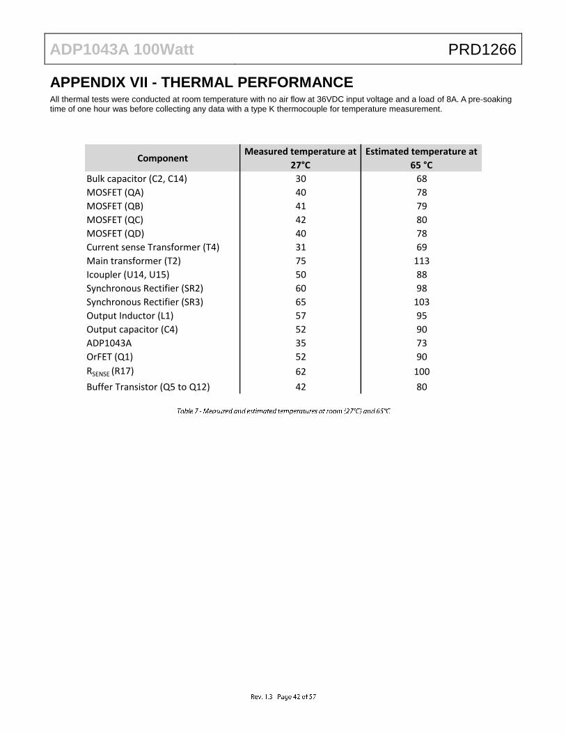
APPENDIX VII - THERMAL PERFORMANCE All thermal tests were conducted at room temperature with no air flow at 36VDC input voltage and a load of 8A. A pre-soaking time of one hour was before collecting any data with a type K thermocouple for temperature measurement.
ComponentMeasured temperature at
27°C
Estimated temperature at
65 °C
Bulk capacitor (C2, C14) 30 68
MOSFET (QA) 40 78
MOSFET (QB) 41 79
MOSFET (QC) 42 80
MOSFET (QD) 40 78
Current sense Transformer (T4) 31 69
Main transformer (T2) 75 113
Icoupler (U14, U15) 50 88
Synchronous Rectifier (SR2) 60 98
Synchronous Rectifier (SR3) 65 103
Output Inductor (L1) 57 95
Output capacitor (C4) 52 90
ADP1043A 35 73
OrFET (Q1) 52 90
RSENSE (R17) 62 100
Buffer Transistor (Q5 to Q12) 42 80

ADP1043A 100Watt PRD1266
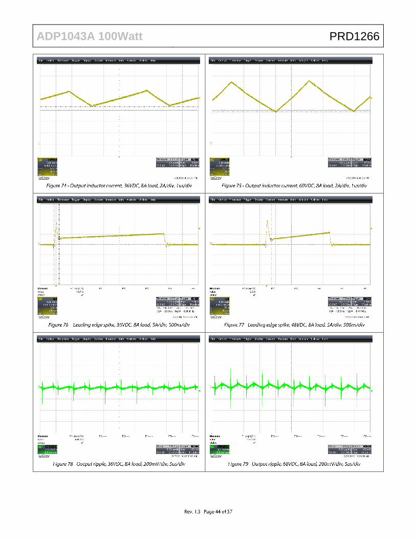
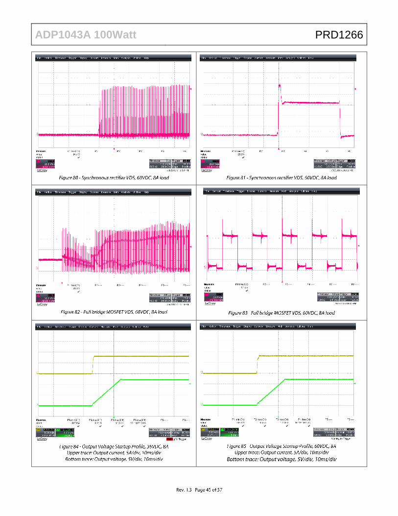
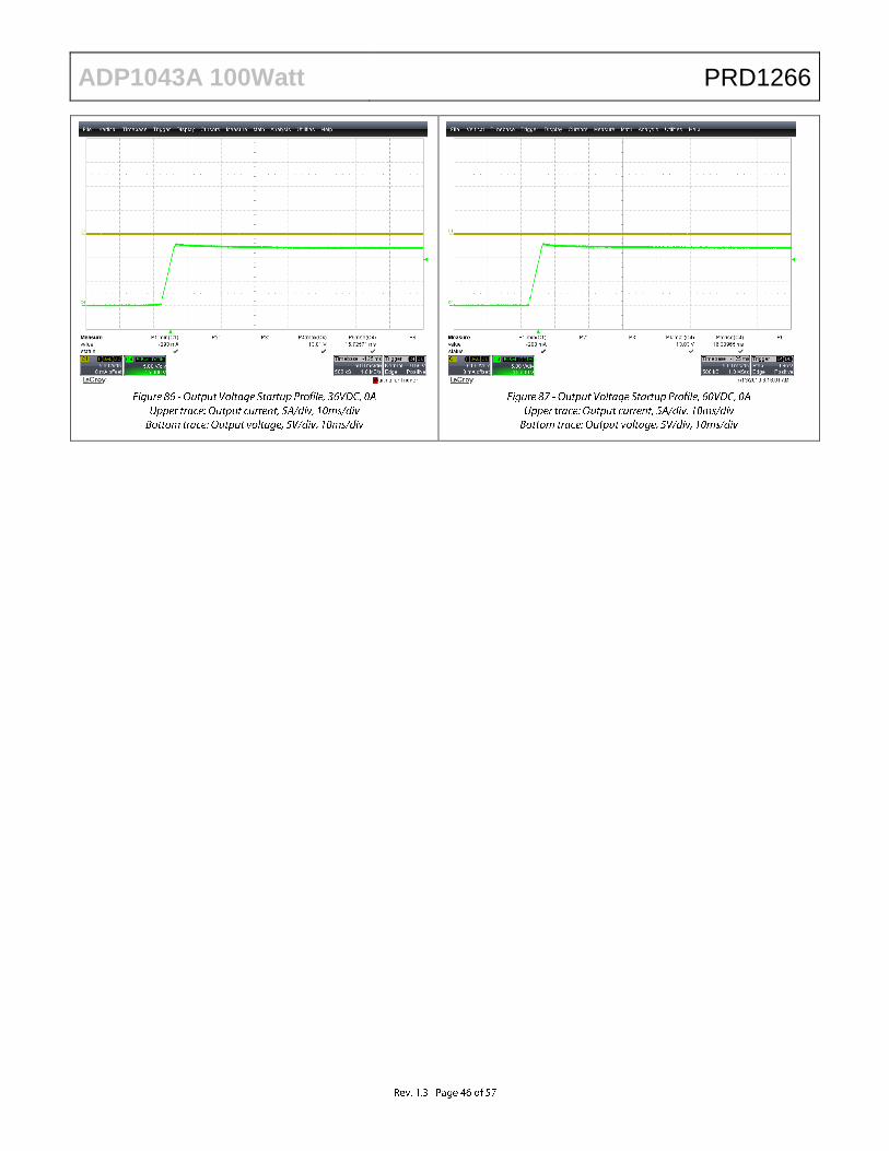
APPENDIX VIII – STEADY STATE WAVEFORMS
ADP1043A 100Watt PRD1266
ADP1043A 100Watt PRD1266
ADP1043A 100Watt PRD1266

ADP1043A 100Watt PRD1266
APPENDIX IX – EFFICIENCY AND VOLTAGE REGULATION
ADP1043A 100Watt PRD1266

ADP1043A 100Watt PRD1266
APPENDIX X – BILL OF MATERIALS (MAIN BOARD)
Part Ref Part Description Package Manufacturer Mfg Part No
C2 CAP 330UF 100V +/-20% ELECTROLYTIC ALUM 18X16.5 Panasonic EEV-FK2A331M
C3 CAP CER 100nF 50V 10% X7R 0805 Murata GRM21BR71H104KA01L
C4 CAP 1500UF 16V ELECT FK SMD 10X1.5 Panasonic EEV-FK1C152Q
C5 CAP CER 2700PF 100V +/-10% X7R 1206 AVX 12061C272KAT2A
C6 CAP CER 1UF 25V +/-10% X7R 0805 Murata GCM21BR71E105KA56L
C7 CAP 1500UF 16V ELECT FK SMD 10X1.5 Panasonic EEV-FK1C152Q
C8 CAP CER 1UF 25V +/-10% X7R 0805 Murata GCM21BR71E105KA56L
C9 DNI
C10 JUMPER WIRE
C11 DNI
C12 CAP CER 2700PF 100V +/-10% X7R 1206 AVX 12061C272KAT2A
C13 CAP CERAMIC 10UF 25V +/-20% X5R 1210 Panasonic ECJ-4YB1E106M
C14 CAP 330UF 100V +/-20% ELECTROLYTIC ALUM 18X16.5 Murata GRM21BR71H104KA01L
C15 CAP CERAMIC 10UF 25V +/-20% X5R 1210 Panasonic ECJ-4YB1E106M
C16 CAP CER 1000pF 100V +/-10% X7R 0805 AVX 08051C102KAT2A
C17 CAP 22UF 25V HA ELECT SMD 5X5.8 Panasonic EEV-HA1E220P
C18 DNI
C19 CAP FILM MKP .015UF 275VAC X2 MKP X2 Vishay BFC233820153
C20 CAP FILM MKP .015UF 275VAC X2 MKP X2 Vishay BFC233820153
C21 DNI
C22 CAP CER 100pF 50V +/-5% NPO 0805 Murata GRM2165C1H101JA01D
C23 CAP FILM 4.7UF 100V +/-5% METAPOLY METALPOLY Panasonic ECQ-E1475KF
C24 CAP CER 100nF 50V 10% X7R 0805 Murata GRM21BR71H104KA01L
C25 DNI
C26 DNI
C27 CAP CERAMIC 4.7UF 25V +/-10% X5R 1210 Panasonic ECJ-4YB1E475K
C28 CAP CERAMIC 1UF 50V +/-10% X7R 1210 Murata GCM21BR71E105KA56L
C29 CAP CERAMIC 1UF 50V +/-10% X7R 1210 Murata GCM21BR71E105KA56L
C30 CAP CERAMIC 4.7UF 25V +/-10% X5R 1210 Panasonic ECJ-4YB1E475K
C31 DNI
C32 CAP CER 390PF 100V +/-5% NPO 0805 Murata GRM2165C2A391JA01D
C33 CAP CER 33PF 50V +/-5% NPO 0805 Panasonic ECJ-2VC1H330J
C34 CAP CER 33PF 50V +/-5% NPO 0805 Panasonic ECJ-2VC1H330J
C35 CAP CER 33PF 50V +/-5% NPO 0805 Panasonic ECJ-2VC1H330J
C36 CAP CERAMIC 10UF 25V +/-20% X5R 1210 Panasonic ECJ-4YB1E106M
C37 CAP CER 33PF 50V +/-5% NPO 0805 Panasonic ECJ-2VC1H330J
C38 CAP CER 0.47UF 25V 10% X7R 0805 TDK C2012X7R1E474K
C39 CAP CERAMIC 10UF 25V +/-20% X5R 1210 Panasonic ECJ-4YB1E106M
C40 CAP CER 0.47UF 25V 10% X7R 0805 TDK C2012X7R1E474K
C41 CAP CER 0.47UF 25V 10% X7R 0805 TDK C2012X7R1E474K
C42 CAP CERAMIC 10UF 25V +/-20% X5R 1210 Panasonic ECJ-4YB1E106M
C43 DNI
C44 CAP CER 100PF 50V +/-5% NPO 0805 Murata GRM2165C1H101JA01D
C45 CAP CER 33PF 50V +/-5% NPO 0805 Panasonic ECJ-2VC1H330J
C46 CAP CER 10000pF 50V +/-10% X7R 0805 Murata GRM216R71H103KA01D
C49 CAP CER 33PF 50V +/-5% NPO 0805 Panasonic ECJ-2VC1H330J
C62 CAP CER 10000PF 50V 10% X7R 0805 Murata GRM216R71H103KA01D
C63 CAP CER 10000PF 50V 10% X7R 0805 Murata GRM216R71H103KA01D
C64 CAP CERAMIC 10UF 25V +/-20% X5R 1210 Panasonic ECJ-4YB1E106M
C67 CAP CERAMIC 10UF 25V +/-20% X5R 1210 Panasonic ECJ-4YB1E106M
C68 DNI
C69 CAP CER 10000PF 50V 10% X7R 0805
C70 CAP CER 0.47uF 25V 10% X7R 0805 TDK C2012X7R1E474K
C71 CAP CER 0.47uF 25V 10% X7R 0805 TDK C2012X7R1E474K
C72 CAP CER 0.47uF 25V 10% X7R 0805 TDK C2012X7R1E474K
D1 LED SUPER RED CLEAR 75MA 1.7V SMD 1206 Chicago miniature lighting CMD15-21SRC/TR8
D2 DIODE SWITCHING 80V 200mA SOT-23 Infenion BAV70E6327
D3 DIODE ZENER 16V 1W 5% MSB-403 Diodes Inc SMAZ16-13-F
D4 DIODE SWITCHING 80V 200mA SOT-23 Infenion BAV70E6327
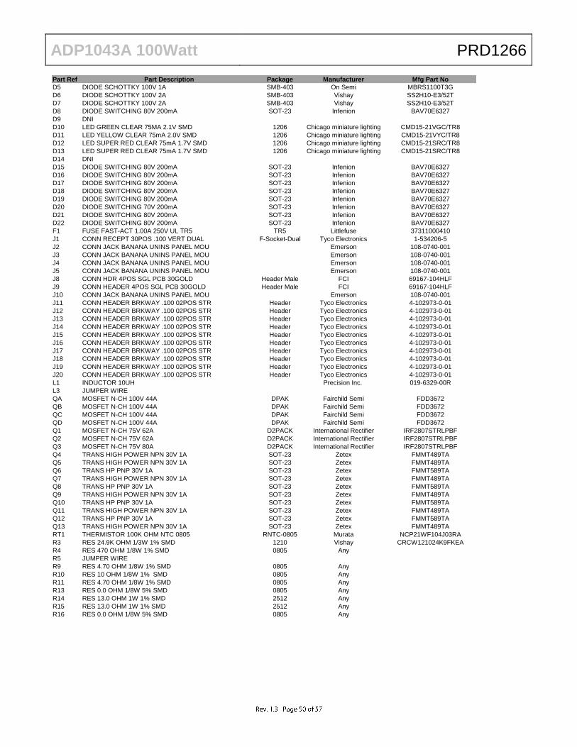
ADP1043A 100Watt PRD1266
Part Ref Part Description Package Manufacturer Mfg Part No
D5 DIODE SCHOTTKY 100V 1A SMB-403 On Semi MBRS1100T3G
D6 DIODE SCHOTTKY 100V 2A SMB-403 Vishay SS2H10-E3/52T
D7 DIODE SCHOTTKY 100V 2A SMB-403 Vishay SS2H10-E3/52T
D8 DIODE SWITCHING 80V 200mA SOT-23 Infenion BAV70E6327
D9 DNI
D10 LED GREEN CLEAR 75MA 2.1V SMD 1206 Chicago miniature lighting CMD15-21VGC/TR8
D11 LED YELLOW CLEAR 75mA 2.0V SMD 1206 Chicago miniature lighting CMD15-21VYC/TR8
D12 LED SUPER RED CLEAR 75mA 1.7V SMD 1206 Chicago miniature lighting CMD15-21SRC/TR8
D13 LED SUPER RED CLEAR 75mA 1.7V SMD 1206 Chicago miniature lighting CMD15-21SRC/TR8
D14 DNI
D15 DIODE SWITCHING 80V 200mA SOT-23 Infenion BAV70E6327
D16 DIODE SWITCHING 80V 200mA SOT-23 Infenion BAV70E6327
D17 DIODE SWITCHING 80V 200mA SOT-23 Infenion BAV70E6327
D18 DIODE SWITCHING 80V 200mA SOT-23 Infenion BAV70E6327
D19 DIODE SWITCHING 80V 200mA SOT-23 Infenion BAV70E6327
D20 DIODE SWITCHING 70V 200mA SOT-23 Infenion BAV70E6327
D21 DIODE SWITCHING 80V 200mA SOT-23 Infenion BAV70E6327
D22 DIODE SWITCHING 80V 200mA SOT-23 Infenion BAV70E6327
F1 FUSE FAST-ACT 1.00A 250V UL TR5 TR5 Littlefuse 37311000410
J1 CONN RECEPT 30POS .100 VERT DUAL F-Socket-Dual Tyco Electronics 1-534206-5
J2 CONN JACK BANANA UNINS PANEL MOU Emerson 108-0740-001
J3 CONN JACK BANANA UNINS PANEL MOU Emerson 108-0740-001
J4 CONN JACK BANANA UNINS PANEL MOU Emerson 108-0740-001
J5 CONN JACK BANANA UNINS PANEL MOU Emerson 108-0740-001
J8 CONN HDR 4POS SGL PCB 30GOLD Header Male FCI 69167-104HLF
J9 CONN HEADER 4POS SGL PCB 30GOLD Header Male FCI 69167-104HLF
J10 CONN JACK BANANA UNINS PANEL MOU Emerson 108-0740-001
J11 CONN HEADER BRKWAY .100 02POS STR Header Tyco Electronics 4-102973-0-01
J12 CONN HEADER BRKWAY .100 02POS STR Header Tyco Electronics 4-102973-0-01
J13 CONN HEADER BRKWAY .100 02POS STR Header Tyco Electronics 4-102973-0-01
J14 CONN HEADER BRKWAY .100 02POS STR Header Tyco Electronics 4-102973-0-01
J15 CONN HEADER BRKWAY .100 02POS STR Header Tyco Electronics 4-102973-0-01
J16 CONN HEADER BRKWAY .100 02POS STR Header Tyco Electronics 4-102973-0-01
J17 CONN HEADER BRKWAY .100 02POS STR Header Tyco Electronics 4-102973-0-01
J18 CONN HEADER BRKWAY .100 02POS STR Header Tyco Electronics 4-102973-0-01
J19 CONN HEADER BRKWAY .100 02POS STR Header Tyco Electronics 4-102973-0-01
J20 CONN HEADER BRKWAY .100 02POS STR Header Tyco Electronics 4-102973-0-01
L1 INDUCTOR 10UH Precision Inc. 019-6329-00R
L3 JUMPER WIRE
QA MOSFET N-CH 100V 44A DPAK Fairchild Semi FDD3672
QB MOSFET N-CH 100V 44A DPAK Fairchild Semi FDD3672
QC MOSFET N-CH 100V 44A DPAK Fairchild Semi FDD3672
QD MOSFET N-CH 100V 44A DPAK Fairchild Semi FDD3672
Q1 MOSFET N-CH 75V 62A D2PACK International Rectifier IRF2807STRLPBF
Q2 MOSFET N-CH 75V 62A D2PACK International Rectifier IRF2807STRLPBF
Q3 MOSFET N-CH 75V 80A D2PACK International Rectifier IRF2807STRLPBF
Q4 TRANS HIGH POWER NPN 30V 1A SOT-23 Zetex FMMT489TA
Q5 TRANS HIGH POWER NPN 30V 1A SOT-23 Zetex FMMT489TA
Q6 TRANS HP PNP 30V 1A SOT-23 Zetex FMMT589TA
Q7 TRANS HIGH POWER NPN 30V 1A SOT-23 Zetex FMMT489TA
Q8 TRANS HP PNP 30V 1A SOT-23 Zetex FMMT589TA
Q9 TRANS HIGH POWER NPN 30V 1A SOT-23 Zetex FMMT489TA
Q10 TRANS HP PNP 30V 1A SOT-23 Zetex FMMT589TA
Q11 TRANS HIGH POWER NPN 30V 1A SOT-23 Zetex FMMT489TA
Q12 TRANS HP PNP 30V 1A SOT-23 Zetex FMMT589TA
Q13 TRANS HIGH POWER NPN 30V 1A SOT-23 Zetex FMMT489TA
RT1 THERMISTOR 100K OHM NTC 0805 RNTC-0805 Murata NCP21WF104J03RA
R3 RES 24.9K OHM 1/3W 1% SMD 1210 Vishay CRCW121024K9FKEA
R4 RES 470 OHM 1/8W 1% SMD 0805 Any
R5 JUMPER WIRE
R9 RES 4.70 OHM 1/8W 1% SMD 0805 Any
R10 RES 10 OHM 1/8W 1% SMD 0805 Any
R11 RES 4.70 OHM 1/8W 1% SMD 0805 Any
R13 RES 0.0 OHM 1/8W 5% SMD 0805 Any
R14 RES 13.0 OHM 1W 1% SMD 2512 Any
R15 RES 13.0 OHM 1W 1% SMD 2512 Any
R16 RES 0.0 OHM 1/8W 5% SMD 0805 Any
ADP1043A 100Watt PRD1266
Part Ref Part Description Package Manufacturer Mfg Part No
R17 RES CURRENT SENSE 0.01 OHM 1W 0.5% SMD 2512 Any
R18 RES 0.0 OHM 1/8W 5% SMD 0805 Any
R19 DNI
R20 DNI
R23 RES 10.0K OHM 1/8W 1% SMD 0805 Any
R24 RES 2.20K OHM 1/8W 1% SMD 0805 Any
R25 DNI
R32 RES 10.0 OHM 1/8W 1% SMD 0805 Any
R34 RES 1.0 OHM 1/8W 1% SMD 0805 Any
R35 RES 8.06K OHM 1/8W 1% SMD 0805 Any
R36 RES 2.05K OHM 1/8W 1% SMD 0805 Any
R37 RES 1.0 OHM 1/8W 1% SMD 0805 Any
R38 RES 10.0 OHM 1/8W 1% SMD 0805 Any
R39 RES 10.0 OHM 1/8W 1% SMD 0805 Any
R40 RES 8.06K OHM 1/8W 1% SMD 0805 Any
R41 RES 10.0K OHM 1/8W 1% SMD 0805 Any
R42 RES 2.05K OHM 1/8W 1% SMD 0805 Any
R43 RES 10.0 OHM 1/8W 1% SMD 0805 Any
R44 RES 10.0 OHM 1/8W 1% SMD 0805 Any
R45 RES 10.0K OHM 1/8W 1% SMD 0805 Any
R46 RES 1.0 OHM 1/8W 1% SMD 0805 Any
R47 RES 1.00K OHM 1/8W 1% SMD 0805 Any
R48 RES 4.7M OHM 1/8W 5% SMD 0805 Any
R49 RES 10.0K OHM 1/8W 1% SMD 0805 Any
R50 RES 10.0K OHM 1/8W 1% SMD 0805 Any
R51 RES 10.0K OHM 1/8W 1% SMD 0805 Any
R52 RES 10.0K OHM 1/8W 1% SMD 0805 Any
R53 RES 2.20K OHM 1/8W 1% SMD 0805 Any
R54 RES 2.20K OHM 1/8W 1% SMD 0805 Any
R55 RES 0.0 OHM 1/2W 5% SMD 2010 Any
R56 RES 0.0 OHM 1/8W 5% SMD 0805 Any
R57 RES 10.0K OHM 1/8W 1% SMD 0805 Any
R58 RES 15.0K OHM 1/8W 1% SMD 0805 Any
R59 RES 100K OHM 1/8W 1% SMD 0805 Any
R60 RES 100 OHM 1/8W 1% SMD 0805 Any
R61 RES 100 OHM 1/8W 1% SMD 0805 Any
R62 RES 2.20K OHM 1/8W 1% SMD 0805 Any
R63 RES 2.20K OHM 1/8W 1% SMD 0805 Any
R64 RES 100 OHM 1/8W 1% SMD 0805 Any
R66 RES 1.00K OHM 1/8W 1% SMD 0805 Any
R67 RES 1.00K OHM 1/8W 1% SMD 0805 Any
R68 RES 470 OHM 1/8W 1% SMD 0805 Any
R70 RES 2.20K OHM 1/8W 1% SMD 0805 Any
R71 RES 0.0 OHM 1/2W 5% SMD 2010 Any
R72 RES 10.0 OHM 1/8W 1% SMD 0805 Any
R73 RES 10.0 OHM 1/8W 1% SMD 0805 Any
R74 RES 10.0K OHM 1/8W 1% SMD 0805 Any
R75 RES 10.0 OHM 1/8W 1% SMD 0805 Any
R76 RES 10.0K OHM 1/8W 1% SMD 0805 Any
R77 RES 10.0K OHM 1/8W 1% SMD 0805 Any
R78 RES 1.00K OHM 1/8W 1% SMD 0805 Any
R79 RES 10.0 OHM 1/8W 1% SMD 0805 Any
R80 RES 100 OHM 1/8W 1% SMD 0805 Any
R81 RES 10.0 OHM 1/8W 1% SMD 0805 Any
SW1 SW SLIDE SPDT 30V 0.2A PC MNT SLIDE-SW Keystone Electronics 5010
TP1-64 TEST POINT PC MULTIPURPOSE RED TP-063 Keystone Electronics 5010
T2 Transformer ETD29 Precision Inc 019-6330-00R
T4 SMT CURRENT SENSE TRANSFORMERS 500kHz 15A PE-68280 Pulse PE-68280
U1 IC MOSFET DRVR DUAL HS 4A 8-SOIC Analog Devices ADP3624
U7A DNI 8-SOIC Analog Devices OP297FSZ
U14 ISOLATED 2CH HALF-BRIDGE DRIVER SOIC-W-16 Analog Devices ADUM5230
U15 ISOLATED 2CH HALF-BRIDGE DRIVER SOIC-W-16 Analog Devices ADUM5230

ADP1043A 100Watt PRD1266
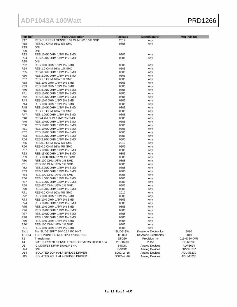
APPENDIX XI – BILL OF MATERIALS (DAUGHTER CARD)
Part Ref Part Description Package Manufacturer Mfg Part No
C1 DNI Murata GRM32RR71H105KA01L
C2 DNI
C3 DNI
C4 DNI
C5 CAPACITOR CERAMIC 1.0UF 50V 10% X7R 1210 Murata GRM32RR71H105KA01L
C6 CAPACITOR CERAMIC 0.1UF 10% 50V X7R 0805 AVX 08055C104KAT2A
C7 DNI
C8 CAPACITOR CERAMIC 0.1UF 10% 50V X7R 0805 AVX 08055C104KAT2A
C9 DNI
C10 DNI
C11 CAPACITOR CERAMIC 0.1UF 10% 50V X7R 0805 AVX 08055C104KAT2A
C12 CAPACITOR CERAMIC 0.47UF 5% 17V X7R 0805 AVX 0805YC474JAT2A
C13 DNI
C14 CAPACITOR CERAMIC 0.01UF 10% 100V X7R 0805 AVX 08051C103KAT2A
C15 CAPACITOR CERAMIC 1000pF 10% 100V X7R 0603 Murata GRM188R72A102KA01D
J1 CONNETOR HEADER FEMALE 30PS .1" DL TIN Fmal Socket
Sullins Connector
Solutions PPTC152LFBN-RC
J7 CONNECTOR HEADER 4POS SGL PCB 30 GOLD Header-4POS FCI 69167-104HLF
R1 RESISTOR 27.0K OHM 1/8W 1% SMD 0805 Any
R2 RESISTOR 1.00K OHM 1/8W 1% SMD 0805 Any
R3 RESISTOR 10.0K OHM 1/10W .1% +/-25ppm SMD 0805 Any
R4 RESISTOR 10.0K OHM 1/10W .1% +/-25ppm SMD 0805 Any
R5 RESISTOR 11.0K OHM 1/10W .1% +/-25ppm SMD 0805 Any
R6 RESISTOR 1.00K OHM 1/10W .1% +/-25ppm SMD 0805 Any
R7 RESISTOR 11.0K OHM 1/10W .1% +/-25ppm SMD 0805 Any
R8 RESISTOR 1.00K OHM 1/10W .1% +/-25ppm SMD 0805 Any
R10 RESISTOR 11.0K OHM 1/10W .1% +/-25ppm SMD 0805 Any
R11 RESISTOR 1.00K OHM 1/10W .1% +/-25ppm SMD 0805 Any
R12 RESISTOR 0.0 OHM 1/8W 5% SMD 0805 Any
R13 RESISTOR 0.0 OHM 1/8W 5% SMD 0805 Any
R14 RESISTOR 1.00K OHM 1/8W 1% SMD 0805 Any
R15 RESISTOR 1.00K OHM 1/8W 1% SMD 0805 Any
R16 RESISTOR 0.0 OHM 1/8W 5% SMD 0805 Any
R17 RESISTOR 0.0 OHM 1/8W 5% SMD 0805 Any
R18 DNI
R19 RESISTOR 10.0K OHM 1/8W 1% SMD 0805 Any
R20 RESISTOR 49.9K OHM 1/8W 1% SMD 0805 Any
R24 RESISTOR 2.20K OHM 1/8W 1% SMD 0805 Any
R29 RESISTOR 2.20K OHM 1/8W 1% SMD 0805 Any
R32 DNI
R33 DNI
U1 I.C. Secondary Side Power Supply Controller LFCSP-32 ADP1043A Analog Devices
U2 I.C. LDO LINEAR REGULATOR 200MA 3.3V SOIC-8 ADP3303 Analog Devices
ADP1043A 100Watt PRD1266
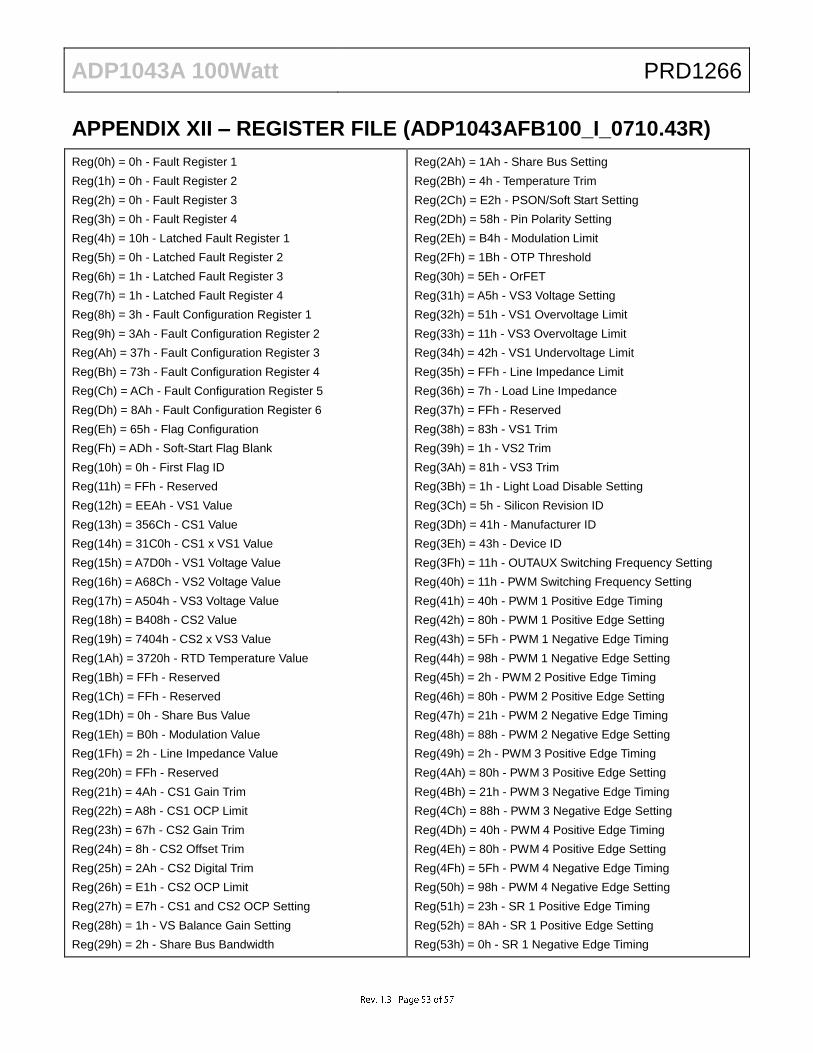
APPENDIX XII – REGISTER FILE (ADP1043AFB100_I_0710.43R)
Reg(0h) = 0h - Fault Register 1
Reg(1h) = 0h - Fault Register 2
Reg(2h) = 0h - Fault Register 3
Reg(3h) = 0h - Fault Register 4
Reg(4h) = 10h - Latched Fault Register 1
Reg(5h) = 0h - Latched Fault Register 2
Reg(6h) = 1h - Latched Fault Register 3
Reg(7h) = 1h - Latched Fault Register 4
Reg(8h) = 3h - Fault Configuration Register 1
Reg(9h) = 3Ah - Fault Configuration Register 2
Reg(Ah) = 37h - Fault Configuration Register 3
Reg(Bh) = 73h - Fault Configuration Register 4
Reg(Ch) = ACh - Fault Configuration Register 5
Reg(Dh) = 8Ah - Fault Configuration Register 6
Reg(Eh) = 65h - Flag Configuration
Reg(Fh) = ADh - Soft-Start Flag Blank
Reg(10h) = 0h - First Flag ID
Reg(11h) = FFh - Reserved
Reg(12h) = EEAh - VS1 Value
Reg(13h) = 356Ch - CS1 Value
Reg(14h) = 31C0h - CS1 x VS1 Value
Reg(15h) = A7D0h - VS1 Voltage Value
Reg(16h) = A68Ch - VS2 Voltage Value
Reg(17h) = A504h - VS3 Voltage Value
Reg(18h) = B408h - CS2 Value
Reg(19h) = 7404h - CS2 x VS3 Value
Reg(1Ah) = 3720h - RTD Temperature Value
Reg(1Bh) = FFh - Reserved
Reg(1Ch) = FFh - Reserved
Reg(1Dh) = 0h - Share Bus Value
Reg(1Eh) = B0h - Modulation Value
Reg(1Fh) = 2h - Line Impedance Value
Reg(20h) = FFh - Reserved
Reg(21h) = 4Ah - CS1 Gain Trim
Reg(22h) = A8h - CS1 OCP Limit
Reg(23h) = 67h - CS2 Gain Trim
Reg(24h) = 8h - CS2 Offset Trim
Reg(25h) = 2Ah - CS2 Digital Trim
Reg(26h) = E1h - CS2 OCP Limit
Reg(27h) = E7h - CS1 and CS2 OCP Setting
Reg(28h) = 1h - VS Balance Gain Setting
Reg(29h) = 2h - Share Bus Bandwidth
Reg(2Ah) = 1Ah - Share Bus Setting
Reg(2Bh) = 4h - Temperature Trim
Reg(2Ch) = E2h - PSON/Soft Start Setting
Reg(2Dh) = 58h - Pin Polarity Setting
Reg(2Eh) = B4h - Modulation Limit
Reg(2Fh) = 1Bh - OTP Threshold
Reg(30h) = 5Eh - OrFET
Reg(31h) = A5h - VS3 Voltage Setting
Reg(32h) = 51h - VS1 Overvoltage Limit
Reg(33h) = 11h - VS3 Overvoltage Limit
Reg(34h) = 42h - VS1 Undervoltage Limit
Reg(35h) = FFh - Line Impedance Limit
Reg(36h) = 7h - Load Line Impedance
Reg(37h) = FFh - Reserved
Reg(38h) = 83h - VS1 Trim
Reg(39h) = 1h - VS2 Trim
Reg(3Ah) = 81h - VS3 Trim
Reg(3Bh) = 1h - Light Load Disable Setting
Reg(3Ch) = 5h - Silicon Revision ID
Reg(3Dh) = 41h - Manufacturer ID
Reg(3Eh) = 43h - Device ID
Reg(3Fh) = 11h - OUTAUX Switching Frequency Setting
Reg(40h) = 11h - PWM Switching Frequency Setting
Reg(41h) = 40h - PWM 1 Positive Edge Timing
Reg(42h) = 80h - PWM 1 Positive Edge Setting
Reg(43h) = 5Fh - PWM 1 Negative Edge Timing
Reg(44h) = 98h - PWM 1 Negative Edge Setting
Reg(45h) = 2h - PWM 2 Positive Edge Timing
Reg(46h) = 80h - PWM 2 Positive Edge Setting
Reg(47h) = 21h - PWM 2 Negative Edge Timing
Reg(48h) = 88h - PWM 2 Negative Edge Setting
Reg(49h) = 2h - PWM 3 Positive Edge Timing
Reg(4Ah) = 80h - PWM 3 Positive Edge Setting
Reg(4Bh) = 21h - PWM 3 Negative Edge Timing
Reg(4Ch) = 88h - PWM 3 Negative Edge Setting
Reg(4Dh) = 40h - PWM 4 Positive Edge Timing
Reg(4Eh) = 80h - PWM 4 Positive Edge Setting
Reg(4Fh) = 5Fh - PWM 4 Negative Edge Timing
Reg(50h) = 98h - PWM 4 Negative Edge Setting
Reg(51h) = 23h - SR 1 Positive Edge Timing
Reg(52h) = 8Ah - SR 1 Positive Edge Setting
Reg(53h) = 0h - SR 1 Negative Edge Timing
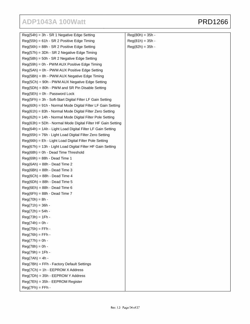
ADP1043A 100Watt PRD1266
Reg(54h) = 3h - SR 1 Negative Edge Setting
Reg(55h) = 61h - SR 2 Positive Edge Timing
Reg(56h) = 88h - SR 2 Positive Edge Setting
Reg(57h) = 3Dh - SR 2 Negative Edge Timing
Reg(58h) = 50h - SR 2 Negative Edge Setting
Reg(59h) = 0h - PWM AUX Positive Edge Timing
Reg(5Ah) = 0h - PWM AUX Positive Edge Setting
Reg(5Bh) = 8h - PWM AUX Negative Edge Timing
Reg(5Ch) = 90h - PWM AUX Negative Edge Setting
Reg(5Dh) = 80h - PWM and SR Pin Disable Setting
Reg(5Eh) = 0h - Password Lock
Reg(5Fh) = 3h - Soft-Start Digital Filter LF Gain Setting
Reg(60h) = 91h - Normal Mode Digital Filter LF Gain Setting
Reg(61h) = 83h - Normal Mode Digital Filter Zero Setting
Reg(62h) = 14h - Normal Mode Digital Filter Pole Setting
Reg(63h) = 5Dh - Normal Mode Digital Filter HF Gain Setting
Reg(64h) = 1Ah - Light Load Digital Filter LF Gain Setting
Reg(65h) = 76h - Light Load Digital Filter Zero Setting
Reg(66h) = Eh - Light Load Digital Filter Pole Setting
Reg(67h) = 13h - Light Load Digital Filter HF Gain Setting
Reg(68h) = 0h - Dead Time Threshold
Reg(69h) = 88h - Dead Time 1
Reg(6Ah) = 88h - Dead Time 2
Reg(6Bh) = 88h - Dead Time 3
Reg(6Ch) = 88h - Dead Time 4
Reg(6Dh) = 88h - Dead Time 5
Reg(6Eh) = 88h - Dead Time 6
Reg(6Fh) = 88h - Dead Time 7
Reg(70h) = 8h -
Reg(71h) = 36h -
Reg(72h) = 54h -
Reg(73h) = 1Fh -
Reg(74h) = 0h -
Reg(75h) = FFh -
Reg(76h) = FFh -
Reg(77h) = 0h -
Reg(78h) = 0h -
Reg(79h) = 1Fh -
Reg(7Ah) = 4h -
Reg(7Bh) = FFh - Factory Default Settings
Reg(7Ch) = 1h - EEPROM X Address
Reg(7Dh) = 35h - EEPROM Y Address
Reg(7Eh) = 35h - EEPROM Register
Reg(7Fh) = FFh -
Reg(80h) = 35h -
Reg(81h) = 35h -
Reg(82h) = 35h -

ADP1043A 100Watt PRD1266
APPENDIX XIII – BOARD FILE (ADP1043AFB100_I_0710.43B) INPUT VOLTAGE = 48 V N1 = 6 N2 = 3 R (CS2) = 11 MOHM I (LOAD) = 8 A R1 = 11 KOHM R2 = 1 KOHM C3 = 1 UF C4 = 1 UF N1 (CS1) = 1 N2 (CS1) = 100 R (CS1) = 10 OHM ESR (L1) = 6 MOHM L1 = 6.5 UH C1 = 1500 UF ESR (C1) = 50 MOHM ESR (L2) = 40 MOHM L2 = 0 UH C2 = 1500 UF ESR (C2) = 50 MOHM R (NORMAL-MODE) (LOAD) = 1.5 OHM R (LIGHT-LOAD-MODE) (LOAD) = 44 OHM CAP ACROSS R1 & R2 = 0 "(1 = YES: 0 = NO)" TOPOLOGY = 0 (0 = FULL BRIDGE: 1 = HALF BRIDGE: 2 = TWO SWITCH FORWARD: 3 = INTERLEAVED TWO SWITCH FORWARD: 4 = ACTIVE CLAMP FORWARD: 5 = RESONANT MODE: 6 = CUSTOM) SWITCHES / DIODES = 0 (0 = SWITCHES: 1 = DIODES) HIGH SIDE / LOW SIDE SENSE (CS2) = 0 (1 = HIGH-SIDE: 0 = LOW-SIDE SENSE) SECOND LC STAGE = 1 (1 = YES: 0 = NO) CS1 INPUT TYPE = 1 (1 = AC: 0 = DC) R3 = 0 KOHM R4 = 0 KOHM PWM MAIN = 0 (0 = OUTA: 1 = OUTB: 2 = OUTC: 3 = OUTD: 4 = SR1: 5 = SR2: 6 = OUTAUX) C5 = 0 UF C6 = 0 UF

ADP1043A 100Watt PRD1266
APPENDIX XIV – CS1 AND CS2 MEASUREMENT VS GUI READING

ADP1043A 100Watt PRD1266
NOTES
©2009 Analog Devices, Inc. All rights reserved. Trademarks and registered trademarks are the property of their respective owners. Error! Unknown document property name.