Embed Size (px)
Citation preview
1SLAU620A–April 2016–Revised May 2016Submit Documentation Feedback
Copyright © 2016, Texas Instruments Incorporated
ADC32RF45/RF80 EVM Quick Startup Guide
Microsoft, Windows are registered trademarks of Microsoft Corporation.LabVIEW is a trademark of National Instruments.
User's GuideSLAU620A–April 2016–Revised May 2016
ADC32RF45/RF80 EVM Quick Startup Guide
This user's guide is a quick-start guide for the ADC32RF45/RF80 EVM. The ADC32RFxx quick-startprocedure using ADC32RF45 bypass LMFS82820, and the ADC32RF80 quick-start procedure (digitalDDC block - decimation plus NCO) external clocking are detailed. A section covering ADC32RF4x/RF80internally generated clocking is also included.
Contents1 Overview ...................................................................................................................... 2
1.1 Required Hardware ................................................................................................. 21.2 Required Software .................................................................................................. 21.3 Evaluation Board Feature Identification Summary ............................................................. 31.4 References .......................................................................................................... 3
2 Quick Start Guide ............................................................................................................ 42.1 Introduction .......................................................................................................... 42.2 Software Installation ................................................................................................ 52.3 Hardware Setup Procedure ....................................................................................... 6
3 ADC32RFxx Quick-Start Procedure ADC32RF45 Bypass LMFS82820 Mode ...................................... 63.1 TSW14J56 ........................................................................................................... 63.2 ADC32RF4x EVM .................................................................................................. 63.3 High Speed Data Converter Pro (HSDC Pro) ................................................................. 12
4 ADC32RF80 Quick-Start Procedure (Digital DDC Block - Decimation Plus NCO) External Clocking .......... 134.1 TSW14J56 ......................................................................................................... 134.2 ADC32RF80 EVM ................................................................................................. 134.3 High Speed Data Converter Pro (HSDC Pro) ................................................................. 18
5 ADC32RF4x/RF80 Internally Generated Clocking ..................................................................... 215.1 ADC32RFxx EVM LMX2582 (or LMX2592) Clocking ........................................................ 215.2 ADC32RFxx EVM LMK04828 Clocking ........................................................................ 21
List of Figures
1 EVM Feature Locations ..................................................................................................... 32 ADC32RFxxEVM GUI Bench Setup Block Diagram .................................................................... 73 ADC32RFxxEVM GUI LMK04828 PLL1 Page........................................................................... 84 ADC32RFxxEVM GUI Low Level Page................................................................................... 95 ADC and LMK Configuration Files ....................................................................................... 106 ADC32RFxxEVM GUI ADC Configuration Tab......................................................................... 117 ADC32RFxxEVM GUI ADC JESD204B Tab ........................................................................... 128 Device Selection LMFS_82820 Mode ................................................................................... 129 Example Capture from Channel A – 5 Sample Mode ................................................................. 1310 ADC32RFxxEVM GUI LMK04828 PLL1 Page ......................................................................... 1411 Low Level Page ............................................................................................................ 1512 ADC32RF4x/ADC32RF80 DDC Configuration Files................................................................... 1513 ADC32RFxxEVM GUI ADC Configuration Tab......................................................................... 1614 ADC32RFxxEVM GUI DDC Configuration Tab ........................................................................ 1715 ADC32RFxxEVM GUI JESD204b Configuration Tab ................................................................. 18

Overview www.ti.com
2 SLAU620A–April 2016–Revised May 2016Submit Documentation Feedback
Copyright © 2016, Texas Instruments Incorporated
ADC32RF45/RF80 EVM Quick Startup Guide
16 Connecting to TSW14J56 ................................................................................................. 1917 Selecting ADC Target Device for TSW14J56 .......................................................................... 1918 Download Firmware........................................................................................................ 1919 Resetting the TSW14J56.................................................................................................. 2020 Popup Window for Setting HSDC Pro Decimation Factor and NCO Frequency................................... 2021 Example Capture From Channel A – 8x Decimation Mode .......................................................... 21
1 OverviewThe ADC32RF45 EVM is an evaluation module (EVM) designed to evaluate the ADC32RF45 family ofhigh-speed, JESD204B interface ADCs. The EVM includes an onboard clocking solution (LMK04828),transformer-coupled analog inputs, full power solution, and easy-to-use software GUI and USB interface.The following features apply to this EVM:• Transformer-coupled signal input network allowing a single-ended signal source from 30 MHz to 3000
MHz.• LMK04828 system clock generator that generates field-programmable gate array (FPGA) reference
clocks for the high-speed serial interface and may optionally be used to generate the ADC samplingclock.
• Transformer-coupled clock input network to test the ADC performance with a very low-noise clocksource
• LMX2582 (or LMX2592) clock synthesizer to generate a very low-noise clock source for clocking theADC32Rf45 ADC.
• High-speed serial data output over a standard FPGA Mezzanine Card (FMC) interface connector.
The ADS54J45 EVM is designed to work seamlessly with TI’s TSW14J56 EVM JESD204B datacapture/pattern generator card, through the High Speed Data Converter Pro (HSDC Pro) software tool forhigh-speed data converter evaluation. The ADC32RF45 EVM is also designed to work with many of thedevelopment kits from leading FPGA vendors that contain an FMC connector.
1.1 Required HardwareThe following equipment is included in the EVM evaluation kit:• ADC32RF45 evaluation board (EVM)• Power supply cable• Mini-USB cable
The following list of equipment are items that are not included in the EVM evaluation kit but are itemsrequired for evaluation of this product in order to achieve the best performance:• TSW14J56EVM data capture board, two 5-V power supplies, and mini-USB cable• Computer running Microsoft® Windows® XP or newer• One low-noise signal generator. Recommendations:
– RF generator, > +17 dBm, < –40 dBc harmonics, < 500 fs jitter 20 kHz–20 MHz, 10-MHz to 3-GHzfrequency rangeExamples: HP HP8644B, Rohde & Schwarz SMA100A
• Bandpass filter for desired analog input. Recommendations:– Bandpass filter, ≥ 60-dB harmonic attenuation, ≤ 5% bandwidth, > +18-dBm power, < 5-dB insertion
lossExamples: Trilithic 5VH-series Tunable BPF, K&L BT-series Tunable BPF, TTE KC6 or KC7-seriesFixed BPF
• Signal path cables, SMA or BNC with BNC-to-SMA adapters
1.2 Required SoftwareThe following software is required to operate the ADC32RF45 EVM and available online. See theReferences section for links.
www.ti.com Overview
3SLAU620A–April 2016–Revised May 2016Submit Documentation Feedback
Copyright © 2016, Texas Instruments Incorporated
ADC32RF45/RF80 EVM Quick Startup Guide
• ADC32RFxx EVM SPI GUI
The following software is required to operate the TSW14J56EVM and available online. See theReferences section for links.• High Speed Data Converter Pro software, version 4.2 or higher
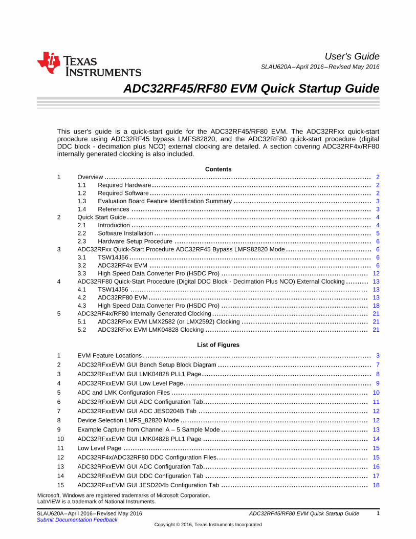
1.3 Evaluation Board Feature Identification SummaryThe EVM features are labeled in Figure 1.
Figure 1. EVM Feature Locations
1.4 ReferencesUse the following links to available documentation and software:• ADC32RFxx EVM software, available from: www.ti.com/tool/ADC32RFxxEVM• ADC32RF45 datasheet (SBAS747)• www.ti.com/product/ADC32RF45• LMK04828 datasheet (SNAS605)• TSW14J56EVM User’s Guide (SLWU086)• High Speed Data Converter Pro software (SLWC107) and User's Guide (SLWU087), available at
www.ti.com/tool/dataconverterpro-sw• HSDC Pro GUI Updates (SLWC106), available at www.ti.com/tool/dataconverterpro-sw
NOTE: The EVM schematics, layout, and BOM are available on the ADC32RFxxEVM tool page onwww.ti.com.
Quick Start Guide www.ti.com
4 SLAU620A–April 2016–Revised May 2016Submit Documentation Feedback
Copyright © 2016, Texas Instruments Incorporated
ADC32RF45/RF80 EVM Quick Startup Guide
2 Quick Start GuideThe EVM test procedure to obtain a valid data capture from the ADC32RF45 EVM using theTSW14J56EVM capture card is provided in this section. This is the starting point for all evaluations.
2.1 IntroductionThe ADC32RF45/RF80 EVM includes the ADC32RF4x or ADC32RF80 analog-to-digital converter withJESD204B interface, and the LMK04828 clock chip to generate the device clock and SYSREF to theADC. Also included on the EVM is the optional LMX2582 or LMX2592 clock synthesizer device. Jumpersand solder options on the EVM allow selection of the ADC sample clock from the LMX2582, theLMK04828, or from a transformer-coupled external SMA input. The default assembly option is thetransformer-coupled external clocking option as set by jumper JP3. The EVM has an FMC connectorsuitable for connection to readily-available FPGA development boards or to the TSW14J56 capture card.
The FPGA on the capture card also requires a device clock and SYSREF signal and the LMK04828 clockdevice also supplies these signals to the FMC connector for that purpose.
This document is meant to convey all information needed to bring up the ADC32RF4x/RF80 EVM andTSW14J56 capture card and get valid data capture with a good FFT result.
The JESD204B interface requires a number of important parameters to be decided in advance of settingup the data link, such as, number of lanes, number of converters, number of samples per frame, and avalue K number of frames per multi-frame, among other parameters. Both sides of a JESD204B link mustbe set up with the same values for all these parameters or else the FPGA that receives the data will notbe able to establish a synchronized link. Getting these parameters inconsistent between ADC andFPGA is perhaps the biggest single reason for an EVM setup to not function as expected. The GUIinstallers that come with the ADC32RF4x/RF80 and the TSW14J56 come with configuration files that aremeant to enable quick initial setup of a number of basic configurations. TI strongly suggests setting upthe EVM and capture card with a configuration described in this document and getting a working setupbefore modifying the configuration to be closer to what the end-application requires. In this way the usercan know that the hardware is functioning, and that there is a working configuration that they can go backto in the event of difficulty developing their own configuration.
The HSDC Pro GUI that comes with the TSW14J56 requires initialization files for both the decimation andmixer logic (called Digital Down-Convert (DDC)) that the ADC32RF80 supports and the non-decimated fullrate mode called LMF82820 or 5-sample mode. (LMF82820 mode means that there are 8 lanes in use for2 channels of ADC, with 8 octets of information on each lane per frame, for 20 samples of data per frameper channel. That is equivalent to 5 samples per lane per frame, hence the mode being called 5 samplemode. 5 samples per lane times 8 lanes is 40 samples, or 20 samples per channel. This mode issometimes called bypass mode because the decimation and mixer logic is bypassed in favor of full rateoutput.) These ini files for HSDC Pro are not included with the HSDC Pro version 4.2 available on the TIweb at this time because the ADC is not a released device. The ini files will have to be manuallycopied into the ADC Files folder for the TSW14J56.Please note that the configuration files for setting up the LMK04828 clocking device are different for theDDC case than they are for the non-decimation (5-sample) case. The different modes of operation of theADC will affect the data rate on the JESD204B interface and thus affect the clocking needed for theFPGA. The configuration files are not interchangeable. For example, theLMK_ADC32RF45_lmfs82820_2457p6_MSPS.cfg file and LMK_ADC32RF80_2457MSPS.cfg file will bothset the sample clock for the ADC at 2.4576 GHz, but the SYSREF and the device clock to the FPGA willbe different for the two files.
This document first introduces the software that must be installed on a PC, and then presents a basicsetup for the ADC32RF80 DDC case, followed by a setup for the ADC32RF45 5-sample mode, bothmodes being clocked by an externally supplied clock, with the LMK04828 clock chip supplying SYSREF tothe ADC and clock/SYSREF to the TSW14J56. The last section covers what to do to supply an internallygenerated sample clock to the ADC, by either the LMK04828 or LMX2582
This document focuses on what is needed to use the HSDC Pro version 4.2 available on the TI web. Laterrevisions of HSDC Pro will likely contain all of the files needed to support the ADC32RF4x/RF80 so thatsome of the manual steps of the following setup would no longer be necessary.

www.ti.com Quick Start Guide
5SLAU620A–April 2016–Revised May 2016Submit Documentation Feedback
Copyright © 2016, Texas Instruments Incorporated
ADC32RF45/RF80 EVM Quick Startup Guide
2.2 Software InstallationThe proper software must be installed before beginning evaluation. See Section 1.2 for a list of therequired software. The References section of this document contains links to find the software on the TIwebsite.
Important: The software must be installed before connecting the ADC32RF45 EVM and TSW14J56 to thecomputer for the first time.
The ADC32RF45/RF80EVM is controlled through an easy-to-use graphical user interface (GUI) to provideaccess to the ADC (ADC32RF45 or ADC32RF80), clock chip (LMK04828), and clock synthesizer(LMX2582 or LMX2592) SPI interfaces. There is a tab in the GUI for each of the devices. This GUIrequires the LabVIEW™ runtime engine, which is automatically installed during the loading of thesoftware.
2.2.1 ADC32RF45 EVM GUI Installation1. Copy the provided installer software called ADC32RFxx EVM GUI Installer.zip (or newer revision on
the TI web, if available) under the ADC32RFxx Customer Files\Software folder to a local host PC.2. Unzip the installer.3. Go to ADC32RF4xx EVM SPI GUI Installer\Volume and double click on setup.exe.4. Follow the installer instructions. After the installer is completed, the executable is located at
“C:\Program Files(86)\Texas Instruments\ADC32RFxx EVM GUI"5. Start the GUI by double clicking on ADC32RFxx EVM GUI.exe or Start Menu → All Programs →
Texas Instruments → ADC32RFxxGUI.6. When plugging the board into the computer for the first time through the USB cable, you may be
prompted to install the USB drivers.• Windows XP: If Windows XP does not automatically install the drivers, follow the prompts on the
screen to do so. Do not let Windows XP search Microsoft Update for the drivers, but do letWindows XP install the drivers automatically.
• Windows 7: After installing the GUI, Windows 7 should automatically be able to install the driversfor the ADC32RFxxEVM with no input from the user.
2.2.2 High Speed Data Converter Pro GUI InstallationHigh Speed Data Converter Pro (HSDC Pro) is used to control the TSW14J56EVM and analyze thecaptured data. Please see the HSDC Pro GUI user’s guide (SLWU087) for more information.1. Download HSDC Pro from the TI website. The References section of this document contains the link to
find the software on the TI website.2. Extract the files from the zip file.3. Run setup.exe and follow the installation prompts.4. If the version of HSDC Pro is 4.1 or lower, download HSDC Pro GUI updates from the TI website. The
References section of this document contains the link to find the software on the TI website.5. Extract the files from the zip file, run HSDC Pro Patch vx.xx.exe and follow the installation instructions.
By default, the HSDC Pro revision 4.1 software does not support unreleased devices such as theADC32RF45 or ADC32RF80 EVM. Newer revisions of HSDC Pro will begin to support the EVM once theEVM is publicly released for order from TI. Until the ADC32RF45 EVM is publicly released, to enablesupport for the EVM:1. Install the HSDC Pro GUI2. Copy the necessary ADC32RFxx ini files to the folder named ‘ADC Files’ in the folder named
‘TSW14J56 Details’ where HSDC Pro is installer. Or if TSW14J56 RevD is being used, copy the inifiles to the ADC Files Folder in the folder named ‘TSW14J56 revD Details’. The ini files for TSW14J56RevB are different than the ini files for TSW14J56 RevD, so be sure to copy the correct files to thecorrect ADC Files folder.
Quick Start Guide www.ti.com
6 SLAU620A–April 2016–Revised May 2016Submit Documentation Feedback
Copyright © 2016, Texas Instruments Incorporated
ADC32RF45/RF80 EVM Quick Startup Guide
2.3 Hardware Setup ProcedureA typical test setup using the ADC32RF45 EVM and TSW14J56EVM is shown in Figure 2. This is the testsetup used for the quick-start procedure.
3 ADC32RFxx Quick-Start Procedure ADC32RF45 Bypass LMFS82820 Mode
3.1 TSW14J56
1. Connect the ADC32RF4x EVM to the TSW14J56 using the FMC connectors.2. Connect a 5-V power supply to connector J11 (+5V IN).3. Connect a USB cable to the USB connector (J9).4. Flip the power switch (SW6) to the “ON” position
3.2 ADC32RF4x EVM1. Verify the clocking selection jumper JP3 is set to EXT for external clocking.2. Connect a 5-V, 3-A power supply to connector J15. Do not use a supply that is rated less than 3 A.3. Connect a USB cable to the USB connector (J11 bottom side of board).4. Connect an analog RF signal from the signal source to the AINP SMA (J2).5. Connect a signal generator set for 2.94912 GHz to the external clock input J5.6. Connect another signal generator set for 2.94912 GHz to the LMK04828 reference clock input J7.
(Make sure the two signal generators for the ADC clock and LMK04828 clock are synchronized to thesame timebase, or use a single signal generator and a splitter to generate two copies of the clock to goto the EVM.)

Analog Input
Low-Noise
Signal Generator
USB 3.0 Cable
+5-VDC Power Supply Cable
PC Running
HSDC Pro
Power
Switch
ADC32RF45 EVM
TSW14J56EVM
Low-Noise
Power Supply
+5 VDC at 3 A
2949.12 MHz, +15 dBmMini-USB Cable
CLK
Analog Input
Low-Noise
Signal Generator
1900 MHz, +15 dBm
2949.12-MHz
Bandpass Filter
1900-MHz
Bandpass Filter
AINP
Low-Noise
Power Supply
+5 VDC at 3 A
www.ti.com ADC32RFxx Quick-Start Procedure ADC32RF45 Bypass LMFS82820 Mode
7SLAU620A–April 2016–Revised May 2016Submit Documentation Feedback
Copyright © 2016, Texas Instruments Incorporated
ADC32RF45/RF80 EVM Quick Startup Guide
Figure 2. ADC32RFxxEVM GUI Bench Setup Block Diagram
Fs = 2.94912 GHz, 5-Sample ExampleThis example captures data from channel A of the ADC32RF45 EVM sampling at 2.94912 GHz with a1900-MHz input source. This procedure uses a .cfg file to set up the LMK04828 clock device first, andthen another .cfg file to set up the ADC. This is always the required sequence. The ADC requires thedevice clock and SYSREF signals to be present before the ADC can be properly configured.1. Open the ADC32RFxx EVM GUI.2. Verify that the green USB Status indicator is lit. If it is not lit, click the Reconnect? button and check the
USB Status indicator again. If it is still not lit then verify the EVM is connected to the computer throughUSB. Whenever the USB link is disturbed, the GUI must obtain a new handle to address the properUSB port, and the Reconnect? Button does that.
3. On the PLL1 tab of the LMK04828 tab, press the RESET button.

ADC32RFxx Quick-Start Procedure ADC32RF45 Bypass LMFS82820 Mode www.ti.com
8 SLAU620A–April 2016–Revised May 2016Submit Documentation Feedback
Copyright © 2016, Texas Instruments Incorporated
ADC32RF45/RF80 EVM Quick Startup Guide
Figure 3. ADC32RFxxEVM GUI LMK04828 PLL1 Page
4. Click on the Low Level View tab.5. Click on the Load Config icon.
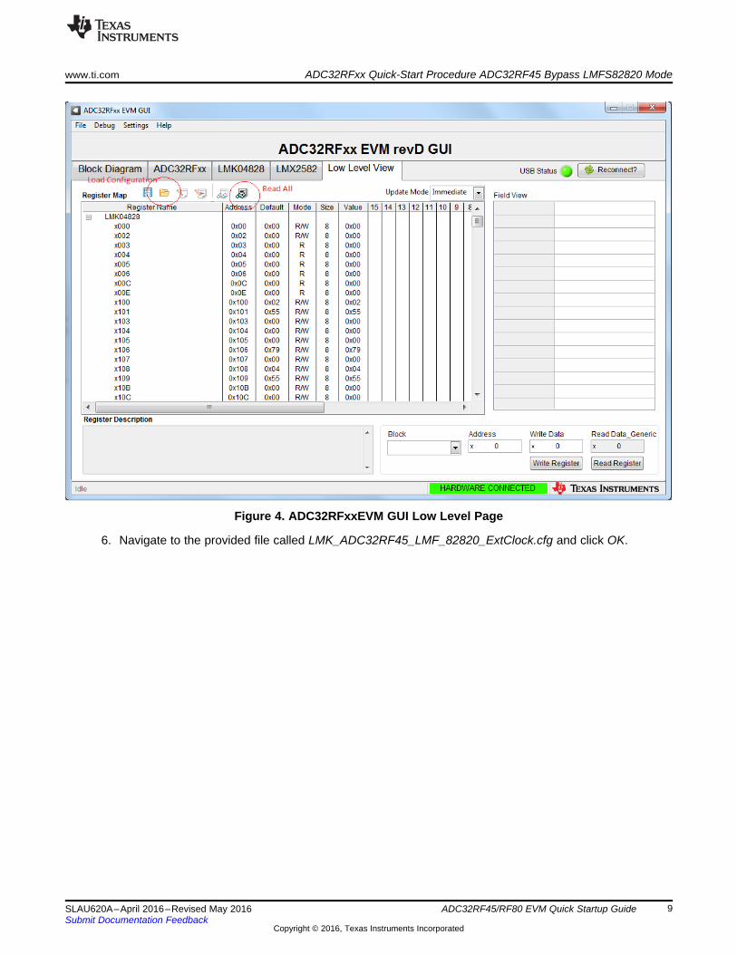
www.ti.com ADC32RFxx Quick-Start Procedure ADC32RF45 Bypass LMFS82820 Mode
9SLAU620A–April 2016–Revised May 2016Submit Documentation Feedback
Copyright © 2016, Texas Instruments Incorporated
ADC32RF45/RF80 EVM Quick Startup Guide
Figure 4. ADC32RFxxEVM GUI Low Level Page
6. Navigate to the provided file called LMK_ADC32RF45_LMF_82820_ExtClock.cfg and click OK.
ADC32RFxx Quick-Start Procedure ADC32RF45 Bypass LMFS82820 Mode www.ti.com
10 SLAU620A–April 2016–Revised May 2016Submit Documentation Feedback
Copyright © 2016, Texas Instruments Incorporated
ADC32RF45/RF80 EVM Quick Startup Guide
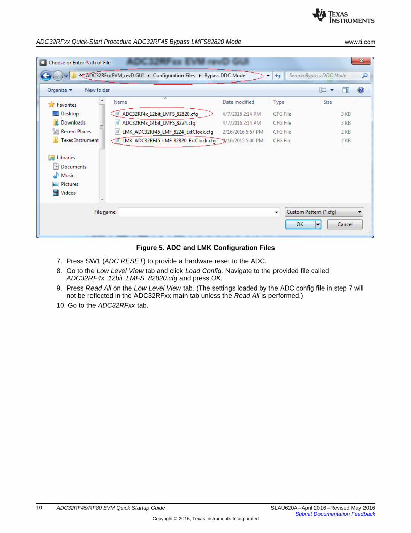
Figure 5. ADC and LMK Configuration Files
7. Press SW1 (ADC RESET) to provide a hardware reset to the ADC.8. Go to the Low Level View tab and click Load Config. Navigate to the provided file called
ADC32RF4x_12bit_LMFS_82820.cfg and press OK.9. Press Read All on the Low Level View tab. (The settings loaded by the ADC config file in step 7 will
not be reflected in the ADC32RFxx main tab unless the Read All is performed.)10. Go to the ADC32RFxx tab.
www.ti.com ADC32RFxx Quick-Start Procedure ADC32RF45 Bypass LMFS82820 Mode
11SLAU620A–April 2016–Revised May 2016Submit Documentation Feedback
Copyright © 2016, Texas Instruments Incorporated
ADC32RF45/RF80 EVM Quick Startup Guide
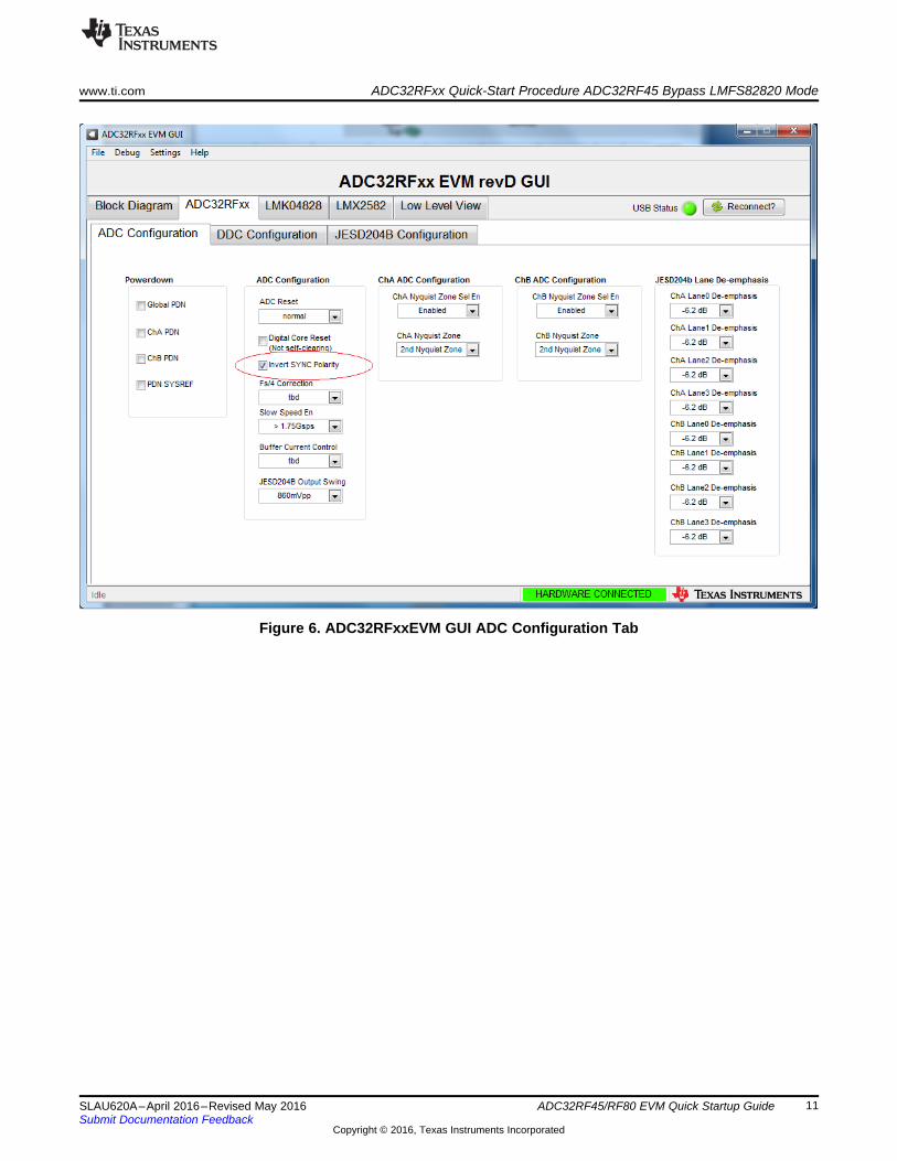
Figure 6. ADC32RFxxEVM GUI ADC Configuration Tab
ADC32RFxx Quick-Start Procedure ADC32RF45 Bypass LMFS82820 Mode www.ti.com
12 SLAU620A–April 2016–Revised May 2016Submit Documentation Feedback
Copyright © 2016, Texas Instruments Incorporated
ADC32RF45/RF80 EVM Quick Startup Guide
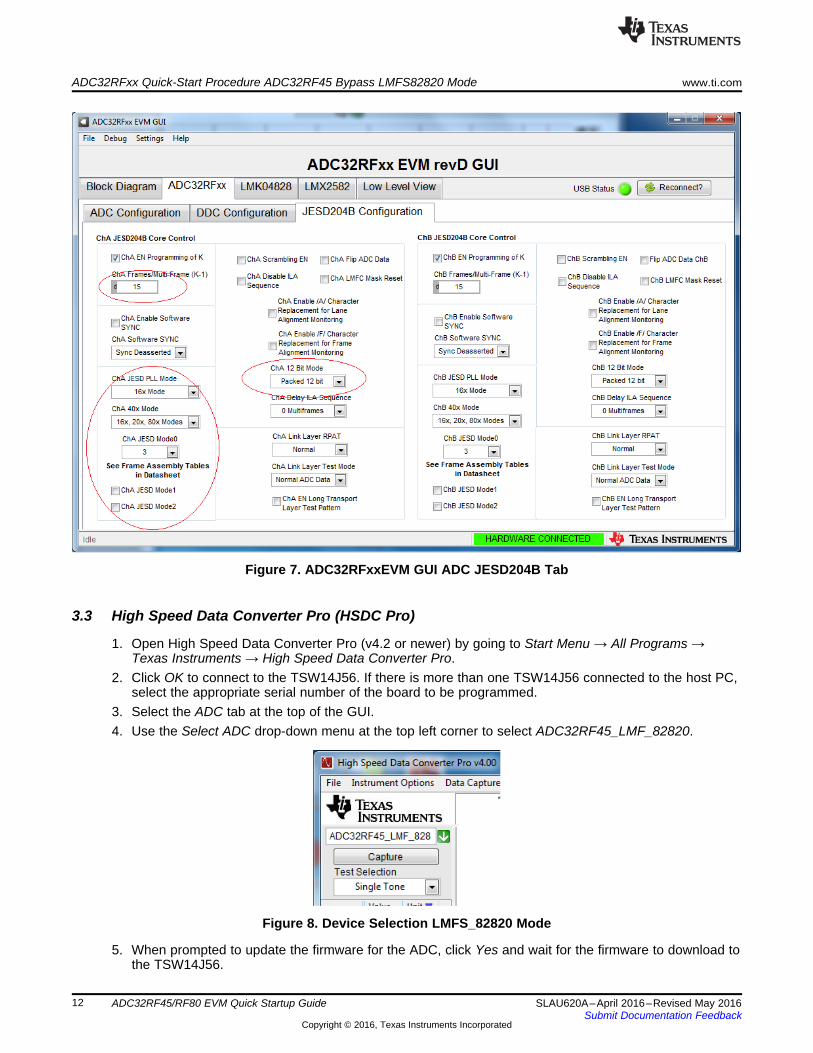
Figure 7. ADC32RFxxEVM GUI ADC JESD204B Tab
3.3 High Speed Data Converter Pro (HSDC Pro)
1. Open High Speed Data Converter Pro (v4.2 or newer) by going to Start Menu → All Programs →Texas Instruments → High Speed Data Converter Pro.
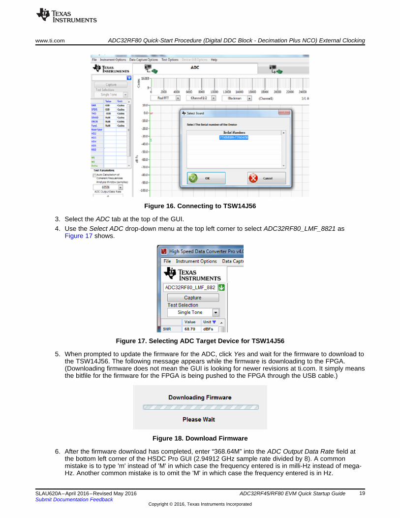
2. Click OK to connect to the TSW14J56. If there is more than one TSW14J56 connected to the host PC,select the appropriate serial number of the board to be programmed.
3. Select the ADC tab at the top of the GUI.4. Use the Select ADC drop-down menu at the top left corner to select ADC32RF45_LMF_82820.
Figure 8. Device Selection LMFS_82820 Mode
5. When prompted to update the firmware for the ADC, click Yes and wait for the firmware to download tothe TSW14J56.

www.ti.com ADC32RF80 Quick-Start Procedure (Digital DDC Block - Decimation Plus NCO) External Clocking
13SLAU620A–April 2016–Revised May 2016Submit Documentation Feedback
Copyright © 2016, Texas Instruments Incorporated
ADC32RF45/RF80 EVM Quick Startup Guide
6. After the firmware download has completed, enter “2949.12M” into the ADC Output Data Rate field atthe bottom left corner of the HSDC Pro GUI.
7. Select “Channel 1/2” in the channel select window located at the top middle of the GUI.8. Click the Instrument Options menu at the top of HSDC Pro and select Reset Board.9. Click Capture in HSDC Pro to capture data from the ADC.10. The result should match the example capture in Figure 9.
Figure 9. Example Capture from Channel A – 5 Sample Mode
4 ADC32RF80 Quick-Start Procedure (Digital DDC Block - Decimation Plus NCO)External Clocking
4.1 TSW14J561. Connect the ADC32RF80 EVM to the TSW14J56 using the FMC connectors.2. Connect a 5-V power supply to connector J11 (+5V IN).3. Connect a USB cable to the USB connector (J9).4. Flip the power switch (SW6) to the “ON” position.
4.2 ADC32RF80 EVM1. Verify jumper JP3 is set for position EXT to select external clocking.2. Connect a 5-V, 3-A power supply to connector J15. Do not use a supply that is rated less than 3 A.3. Connect a USB cable to the USB connector (J11 bottom side of board).4. Connect an analog RF signal from a signal source to the AINP SMA (J2).5. Connect a signal generator set for 2.94912 GHz to the external clock input J5.6. Connect another signal generator set for 2.94912 GHz to the LMK04828 reference clock input J7.
(Make sure the two signal generators for the ADC clock and LMK04828 clock are synchronized to thesame timebase, or use a single signal generator and a splitter to generate two copies of the clock to goto the EVM.)
ADC32RF80 Quick-Start Procedure (Digital DDC Block - Decimation Plus NCO) External Clocking www.ti.com
14 SLAU620A–April 2016–Revised May 2016Submit Documentation Feedback
Copyright © 2016, Texas Instruments Incorporated
ADC32RF45/RF80 EVM Quick Startup Guide
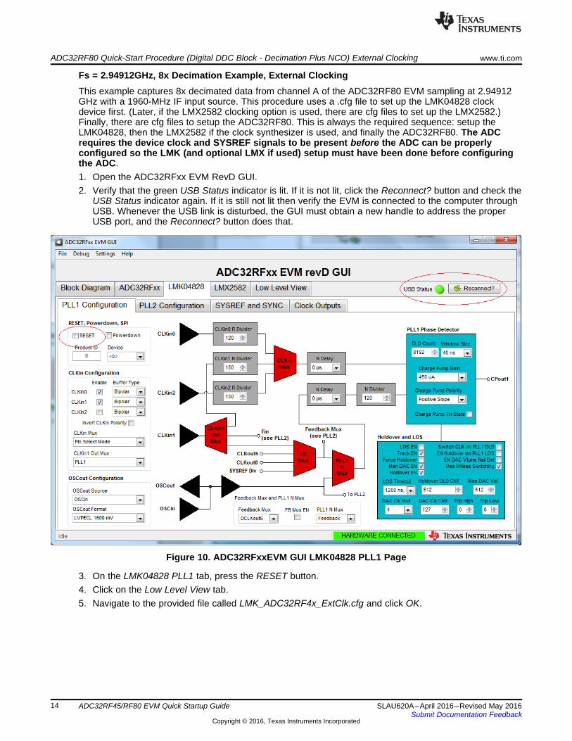
Fs = 2.94912GHz, 8x Decimation Example, External ClockingThis example captures 8x decimated data from channel A of the ADC32RF80 EVM sampling at 2.94912GHz with a 1960-MHz IF input source. This procedure uses a .cfg file to set up the LMK04828 clockdevice first. (Later, if the LMX2582 clocking option is used, there are cfg files to set up the LMX2582.)Finally, there are cfg files to setup the ADC32RF80. This is always the required sequence: setup theLMK04828, then the LMX2582 if the clock synthesizer is used, and finally the ADC32RF80. The ADCrequires the device clock and SYSREF signals to be present before the ADC can be properlyconfigured so the LMK (and optional LMX if used) setup must have been done before configuringthe ADC.1. Open the ADC32RFxx EVM RevD GUI.2. Verify that the green USB Status indicator is lit. If it is not lit, click the Reconnect? button and check the
USB Status indicator again. If it is still not lit then verify the EVM is connected to the computer throughUSB. Whenever the USB link is disturbed, the GUI must obtain a new handle to address the properUSB port, and the Reconnect? button does that.
Figure 10. ADC32RFxxEVM GUI LMK04828 PLL1 Page
3. On the LMK04828 PLL1 tab, press the RESET button.4. Click on the Low Level View tab.5. Navigate to the provided file called LMK_ADC32RF4x_ExtClk.cfg and click OK.

www.ti.com ADC32RF80 Quick-Start Procedure (Digital DDC Block - Decimation Plus NCO) External Clocking
15SLAU620A–April 2016–Revised May 2016Submit Documentation Feedback
Copyright © 2016, Texas Instruments Incorporated
ADC32RF45/RF80 EVM Quick Startup Guide
Figure 11. Low Level Page
Figure 12. ADC32RF4x/ADC32RF80 DDC Configuration Files
ADC32RF80 Quick-Start Procedure (Digital DDC Block - Decimation Plus NCO) External Clocking www.ti.com
16 SLAU620A–April 2016–Revised May 2016Submit Documentation Feedback
Copyright © 2016, Texas Instruments Incorporated
ADC32RF45/RF80 EVM Quick Startup Guide
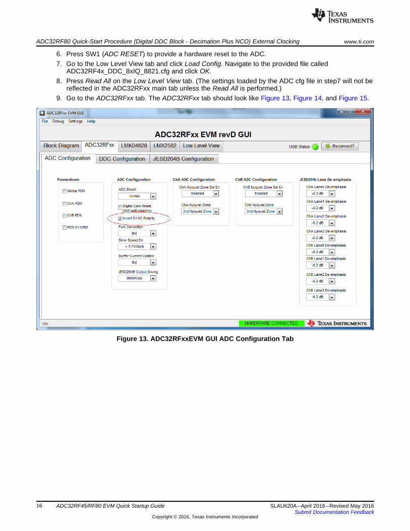
6. Press SW1 (ADC RESET) to provide a hardware reset to the ADC.7. Go to the Low Level View tab and click Load Config. Navigate to the provided file called
ADC32RF4x_DDC_8xIQ_8821.cfg and click OK.8. Press Read All on the Low Level View tab. (The settings loaded by the ADC cfg file in step7 will not be
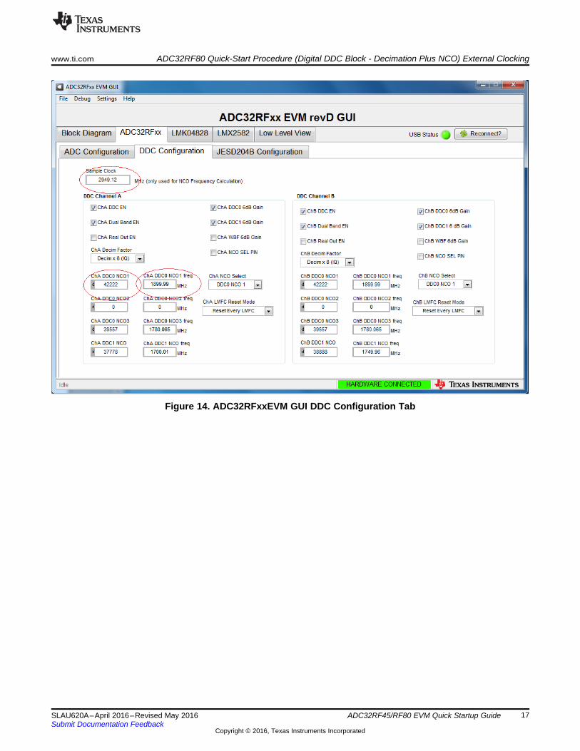
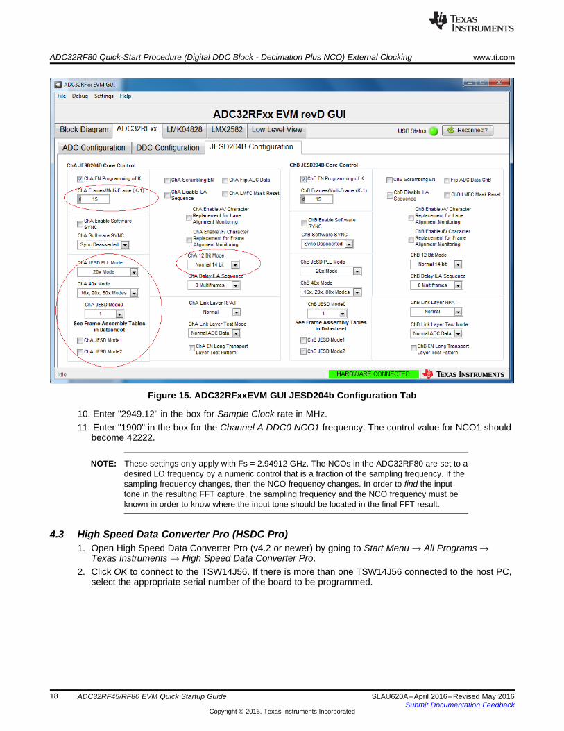
reflected in the ADC32RFxx main tab unless the Read All is performed.)9. Go to the ADC32RFxx tab. The ADC32RFxx tab should look like Figure 13, Figure 14, and Figure 15.
Figure 13. ADC32RFxxEVM GUI ADC Configuration Tab
www.ti.com ADC32RF80 Quick-Start Procedure (Digital DDC Block - Decimation Plus NCO) External Clocking
17SLAU620A–April 2016–Revised May 2016Submit Documentation Feedback
Copyright © 2016, Texas Instruments Incorporated
ADC32RF45/RF80 EVM Quick Startup Guide
Figure 14. ADC32RFxxEVM GUI DDC Configuration Tab
ADC32RF80 Quick-Start Procedure (Digital DDC Block - Decimation Plus NCO) External Clocking www.ti.com
18 SLAU620A–April 2016–Revised May 2016Submit Documentation Feedback
Copyright © 2016, Texas Instruments Incorporated
ADC32RF45/RF80 EVM Quick Startup Guide
Figure 15. ADC32RFxxEVM GUI JESD204b Configuration Tab
10. Enter "2949.12" in the box for Sample Clock rate in MHz.11. Enter "1900" in the box for the Channel A DDC0 NCO1 frequency. The control value for NCO1 should
become 42222.
NOTE: These settings only apply with Fs = 2.94912 GHz. The NCOs in the ADC32RF80 are set to adesired LO frequency by a numeric control that is a fraction of the sampling frequency. If thesampling frequency changes, then the NCO frequency changes. In order to find the inputtone in the resulting FFT capture, the sampling frequency and the NCO frequency must beknown in order to know where the input tone should be located in the final FFT result.
4.3 High Speed Data Converter Pro (HSDC Pro)1. Open High Speed Data Converter Pro (v4.2 or newer) by going to Start Menu → All Programs →
Texas Instruments → High Speed Data Converter Pro.2. Click OK to connect to the TSW14J56. If there is more than one TSW14J56 connected to the host PC,
select the appropriate serial number of the board to be programmed.
www.ti.com ADC32RF80 Quick-Start Procedure (Digital DDC Block - Decimation Plus NCO) External Clocking
19SLAU620A–April 2016–Revised May 2016Submit Documentation Feedback
Copyright © 2016, Texas Instruments Incorporated
ADC32RF45/RF80 EVM Quick Startup Guide
Figure 16. Connecting to TSW14J56
3. Select the ADC tab at the top of the GUI.4. Use the Select ADC drop-down menu at the top left corner to select ADC32RF80_LMF_8821 as
Figure 17 shows.
Figure 17. Selecting ADC Target Device for TSW14J56
5. When prompted to update the firmware for the ADC, click Yes and wait for the firmware to download tothe TSW14J56. The following message appears while the firmware is downloading to the FPGA.(Downloading firmware does not mean the GUI is looking for newer revisions at ti.com. It simply meansthe bitfile for the firmware for the FPGA is being pushed to the FPGA through the USB cable.)
Figure 18. Download Firmware
6. After the firmware download has completed, enter “368.64M” into the ADC Output Data Rate field atthe bottom left corner of the HSDC Pro GUI (2.94912 GHz sample rate divided by 8). A commonmistake is to type 'm' instead of 'M' in which case the frequency entered is in milli-Hz instead of mega-Hz. Another common mistake is to omit the 'M' in which case the frequency entered is in Hz.

ADC32RF80 Quick-Start Procedure (Digital DDC Block - Decimation Plus NCO) External Clocking www.ti.com
20 SLAU620A–April 2016–Revised May 2016Submit Documentation Feedback
Copyright © 2016, Texas Instruments Incorporated
ADC32RF45/RF80 EVM Quick Startup Guide
7. Select “Channel 1/8” in the channel select window located at the top middle of the GUI.8. Click the Instrument Options menu at the top of HSDC Pro and select Reset Board.
Figure 19. Resetting the TSW14J56
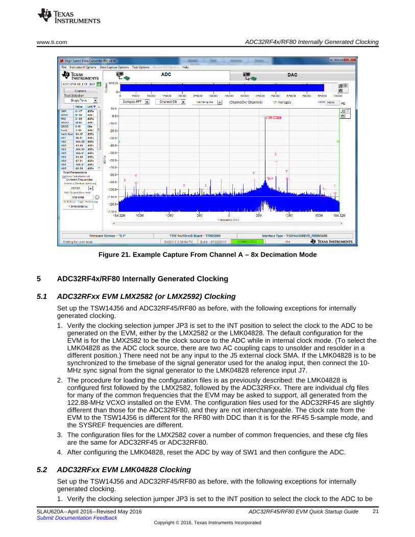
9. Click Capture in HSDC Pro to capture data from the ADC.10. Select Complex FFT11. The result should match the example capture in Figure 21.
The input tone is seen to be near 60 MHz because the signal generator is set to 1.96 GHz while weset the NCO in the ADC to 1.90 GHz. So, the input tone is mixed down to 60 MHz. If the signalgenerators for the analog input tone and the clocking are synchronized, then HSDC Pro is able tolocate the expected tone after the NCO and decimation by way of the popup parameter window ofFigure 20. If this popup is used, the frequency values entered must be exact.
Figure 20. Popup Window for Setting HSDC Pro Decimation Factor and NCO Frequency
www.ti.com ADC32RF4x/RF80 Internally Generated Clocking
21SLAU620A–April 2016–Revised May 2016Submit Documentation Feedback
Copyright © 2016, Texas Instruments Incorporated
ADC32RF45/RF80 EVM Quick Startup Guide
Figure 21. Example Capture From Channel A – 8x Decimation Mode
5 ADC32RF4x/RF80 Internally Generated Clocking
5.1 ADC32RFxx EVM LMX2582 (or LMX2592) ClockingSet up the TSW14J56 and ADC32RF45/RF80 as before, with the following exceptions for internallygenerated clocking.1. Verify the clocking selection jumper JP3 is set to the INT position to select the clock to the ADC to be
generated on the EVM, either by the LMX2582 or the LMK04828. The default configuration for theEVM is for the LMX2582 to be the clock source to the ADC while in internal clock mode. (To select theLMK04828 as the ADC clock source, there are two AC coupling caps to unsolder and resolder in adifferent position.) There need not be any input to the J5 external clock SMA. If the LMK04828 is to besynchronized to the timebase of the signal generator used for the analog input, then connect the 10-MHz sync signal from the signal generator to the LMK04828 reference input J7.
2. The procedure for loading the configuration files is as previously described: the LMK04828 isconfigured first followed by the LMX2582, followed by the ADC32RFxx. There are individual cfg filesfor many of the common frequencies that the EVM may be asked to support, all generated from the122.88-MHz VCXO installed on the EVM. The configuration files used for the ADC32RF45 are slightlydifferent than those for the ADC32RF80, and they are not interchangeable. The clock rate from theEVM to the TSW14J56 is different for the RF80 with DDC than it is for the RF45 5-sample mode, andthe SYSREF frequencies are different.
3. The configuration files for the LMX2582 cover a number of common frequencies, and these cfg filesare the same for ADC32RF45 or ADC32RF80.
4. After configuring the LMK04828, reset the ADC by way of SW1 and then configure the ADC.
5.2 ADC32RFxx EVM LMK04828 ClockingSet up the TSW14J56 and ADC32RF45/RF80 as before, with the following exceptions for internallygenerated clocking.1. Verify the clocking selection jumper JP3 is set to the INT position to select the clock to the ADC to be

Revision History www.ti.com
22 SLAU620A–April 2016–Revised May 2016Submit Documentation Feedback
Copyright © 2016, Texas Instruments Incorporated
Revision History
generated on the EVM, either by the LMX2582 or the LMK04828. The default configuration for theEVM is for the LMX2582 to be the clock source to the ADC while in internal clock mode. Unsolder thetwo AC coupling caps from positions C409 and C410 and solder them into positions C431 and C432.This disconnects the ADC device clock from the LMX2582 outputs and instead connects theLMK04828 device clock output to be the clock source to the ADC. There need not be any input to theJ5 external clock SMA. If the LMK04828 is to be synchronized to the timebase of the signal generatorused for the analog input, then connect the 10-MHz sync signal from the signal generator to theLMK04828 reference input J7. The LMK04828 is still used to supply SYSREF to the ADC andClock/SYSREF to the TSW14J56.
2. The procedure for loading the configuration files is as previously described: the LMK04828 isconfigured, followed by the ADC32RFxx. There are individual cfg files for many of the commonfrequencies that the EVM may be asked to support, all generated from the 122.88-MHz VCXO installedon the EVM. The configuration files used for the ADC32RF45 are slightly different than those for theADC32RF80, and they are not interchangeable. The clock rate from the EVM to the TSW14J56 isdifferent for the RF80 with DDC than it is for the RF45 5-sample mode, and the SYSREF frequenciesare different. Also, the LMK04828 is configured to pass a copy of the 122.88 VCXO reference on to theLMX2582.
3. After configuring the LMK04828, reset the ADC by way of SW1 and then configure the ADC.
Revision HistoryNOTE: Page numbers for previous revisions may differ from page numbers in the current version.
Changes from Original (April 2016) to A Revision .......................................................................................................... Page
• Updated EVM Feature Locations image................................................................................................ 3• Deleted example test setup image. ..................................................................................................... 6• Updated ADC32RFxxEVM GUI Bench Setup Block Diagram image............................................................... 7• Updated Example Capture from Channel A – 5 Sample Mode image............................................................ 13• Updated Example Capture From Channel A – 8x Decimation Mode image. .................................................... 21

STANDARD TERMS AND CONDITIONS FOR EVALUATION MODULES1. Delivery: TI delivers TI evaluation boards, kits, or modules, including any accompanying demonstration software, components, or
documentation (collectively, an “EVM” or “EVMs”) to the User (“User”) in accordance with the terms and conditions set forth herein.Acceptance of the EVM is expressly subject to the following terms and conditions.1.1 EVMs are intended solely for product or software developers for use in a research and development setting to facilitate feasibility
evaluation, experimentation, or scientific analysis of TI semiconductors products. EVMs have no direct function and are notfinished products. EVMs shall not be directly or indirectly assembled as a part or subassembly in any finished product. Forclarification, any software or software tools provided with the EVM (“Software”) shall not be subject to the terms and conditionsset forth herein but rather shall be subject to the applicable terms and conditions that accompany such Software
1.2 EVMs are not intended for consumer or household use. EVMs may not be sold, sublicensed, leased, rented, loaned, assigned,or otherwise distributed for commercial purposes by Users, in whole or in part, or used in any finished product or productionsystem.
2 Limited Warranty and Related Remedies/Disclaimers:2.1 These terms and conditions do not apply to Software. The warranty, if any, for Software is covered in the applicable Software
License Agreement.2.2 TI warrants that the TI EVM will conform to TI's published specifications for ninety (90) days after the date TI delivers such EVM
to User. Notwithstanding the foregoing, TI shall not be liable for any defects that are caused by neglect, misuse or mistreatmentby an entity other than TI, including improper installation or testing, or for any EVMs that have been altered or modified in anyway by an entity other than TI. Moreover, TI shall not be liable for any defects that result from User's design, specifications orinstructions for such EVMs. Testing and other quality control techniques are used to the extent TI deems necessary or asmandated by government requirements. TI does not test all parameters of each EVM.
2.3 If any EVM fails to conform to the warranty set forth above, TI's sole liability shall be at its option to repair or replace such EVM,or credit User's account for such EVM. TI's liability under this warranty shall be limited to EVMs that are returned during thewarranty period to the address designated by TI and that are determined by TI not to conform to such warranty. If TI elects torepair or replace such EVM, TI shall have a reasonable time to repair such EVM or provide replacements. Repaired EVMs shallbe warranted for the remainder of the original warranty period. Replaced EVMs shall be warranted for a new full ninety (90) daywarranty period.
3 Regulatory Notices:3.1 United States
3.1.1 Notice applicable to EVMs not FCC-Approved:This kit is designed to allow product developers to evaluate electronic components, circuitry, or software associated with the kitto determine whether to incorporate such items in a finished product and software developers to write software applications foruse with the end product. This kit is not a finished product and when assembled may not be resold or otherwise marketed unlessall required FCC equipment authorizations are first obtained. Operation is subject to the condition that this product not causeharmful interference to licensed radio stations and that this product accept harmful interference. Unless the assembled kit isdesigned to operate under part 15, part 18 or part 95 of this chapter, the operator of the kit must operate under the authority ofan FCC license holder or must secure an experimental authorization under part 5 of this chapter.3.1.2 For EVMs annotated as FCC – FEDERAL COMMUNICATIONS COMMISSION Part 15 Compliant:
CAUTIONThis device complies with part 15 of the FCC Rules. Operation is subject to the following two conditions: (1) This device may notcause harmful interference, and (2) this device must accept any interference received, including interference that may causeundesired operation.Changes or modifications not expressly approved by the party responsible for compliance could void the user's authority tooperate the equipment.
FCC Interference Statement for Class A EVM devicesNOTE: This equipment has been tested and found to comply with the limits for a Class A digital device, pursuant to part 15 ofthe FCC Rules. These limits are designed to provide reasonable protection against harmful interference when the equipment isoperated in a commercial environment. This equipment generates, uses, and can radiate radio frequency energy and, if notinstalled and used in accordance with the instruction manual, may cause harmful interference to radio communications.Operation of this equipment in a residential area is likely to cause harmful interference in which case the user will be required tocorrect the interference at his own expense.
SPACER
SPACER
SPACER
SPACER
SPACER
SPACER
SPACER
SPACER
FCC Interference Statement for Class B EVM devicesNOTE: This equipment has been tested and found to comply with the limits for a Class B digital device, pursuant to part 15 ofthe FCC Rules. These limits are designed to provide reasonable protection against harmful interference in a residentialinstallation. This equipment generates, uses and can radiate radio frequency energy and, if not installed and used in accordancewith the instructions, may cause harmful interference to radio communications. However, there is no guarantee that interferencewill not occur in a particular installation. If this equipment does cause harmful interference to radio or television reception, whichcan be determined by turning the equipment off and on, the user is encouraged to try to correct the interference by one or moreof the following measures:
• Reorient or relocate the receiving antenna.• Increase the separation between the equipment and receiver.• Connect the equipment into an outlet on a circuit different from that to which the receiver is connected.• Consult the dealer or an experienced radio/TV technician for help.
3.2 Canada3.2.1 For EVMs issued with an Industry Canada Certificate of Conformance to RSS-210
Concerning EVMs Including Radio Transmitters:This device complies with Industry Canada license-exempt RSS standard(s). Operation is subject to the following two conditions:(1) this device may not cause interference, and (2) this device must accept any interference, including interference that maycause undesired operation of the device.
Concernant les EVMs avec appareils radio:Le présent appareil est conforme aux CNR d'Industrie Canada applicables aux appareils radio exempts de licence. L'exploitationest autorisée aux deux conditions suivantes: (1) l'appareil ne doit pas produire de brouillage, et (2) l'utilisateur de l'appareil doitaccepter tout brouillage radioélectrique subi, même si le brouillage est susceptible d'en compromettre le fonctionnement.
Concerning EVMs Including Detachable Antennas:Under Industry Canada regulations, this radio transmitter may only operate using an antenna of a type and maximum (or lesser)gain approved for the transmitter by Industry Canada. To reduce potential radio interference to other users, the antenna typeand its gain should be so chosen that the equivalent isotropically radiated power (e.i.r.p.) is not more than that necessary forsuccessful communication. This radio transmitter has been approved by Industry Canada to operate with the antenna typeslisted in the user guide with the maximum permissible gain and required antenna impedance for each antenna type indicated.Antenna types not included in this list, having a gain greater than the maximum gain indicated for that type, are strictly prohibitedfor use with this device.
Concernant les EVMs avec antennes détachablesConformément à la réglementation d'Industrie Canada, le présent émetteur radio peut fonctionner avec une antenne d'un type etd'un gain maximal (ou inférieur) approuvé pour l'émetteur par Industrie Canada. Dans le but de réduire les risques de brouillageradioélectrique à l'intention des autres utilisateurs, il faut choisir le type d'antenne et son gain de sorte que la puissance isotroperayonnée équivalente (p.i.r.e.) ne dépasse pas l'intensité nécessaire à l'établissement d'une communication satisfaisante. Leprésent émetteur radio a été approuvé par Industrie Canada pour fonctionner avec les types d'antenne énumérés dans lemanuel d’usage et ayant un gain admissible maximal et l'impédance requise pour chaque type d'antenne. Les types d'antennenon inclus dans cette liste, ou dont le gain est supérieur au gain maximal indiqué, sont strictement interdits pour l'exploitation del'émetteur
3.3 Japan3.3.1 Notice for EVMs delivered in Japan: Please see http://www.tij.co.jp/lsds/ti_ja/general/eStore/notice_01.page 日本国内に
輸入される評価用キット、ボードについては、次のところをご覧ください。http://www.tij.co.jp/lsds/ti_ja/general/eStore/notice_01.page
3.3.2 Notice for Users of EVMs Considered “Radio Frequency Products” in Japan: EVMs entering Japan may not be certifiedby TI as conforming to Technical Regulations of Radio Law of Japan.
If User uses EVMs in Japan, not certified to Technical Regulations of Radio Law of Japan, User is required by Radio Law ofJapan to follow the instructions below with respect to EVMs:1. Use EVMs in a shielded room or any other test facility as defined in the notification #173 issued by Ministry of Internal
Affairs and Communications on March 28, 2006, based on Sub-section 1.1 of Article 6 of the Ministry’s Rule forEnforcement of Radio Law of Japan,
2. Use EVMs only after User obtains the license of Test Radio Station as provided in Radio Law of Japan with respect toEVMs, or
3. Use of EVMs only after User obtains the Technical Regulations Conformity Certification as provided in Radio Law of Japanwith respect to EVMs. Also, do not transfer EVMs, unless User gives the same notice above to the transferee. Please notethat if User does not follow the instructions above, User will be subject to penalties of Radio Law of Japan.
SPACER
SPACER
SPACER
SPACER
SPACER
【無線電波を送信する製品の開発キットをお使いになる際の注意事項】 開発キットの中には技術基準適合証明を受けていないものがあります。 技術適合証明を受けていないもののご使用に際しては、電波法遵守のため、以下のいずれかの措置を取っていただく必要がありますのでご注意ください。1. 電波法施行規則第6条第1項第1号に基づく平成18年3月28日総務省告示第173号で定められた電波暗室等の試験設備でご使用
いただく。2. 実験局の免許を取得後ご使用いただく。3. 技術基準適合証明を取得後ご使用いただく。
なお、本製品は、上記の「ご使用にあたっての注意」を譲渡先、移転先に通知しない限り、譲渡、移転できないものとします。上記を遵守頂けない場合は、電波法の罰則が適用される可能性があることをご留意ください。 日本テキサス・イ
ンスツルメンツ株式会社東京都新宿区西新宿6丁目24番1号西新宿三井ビル
3.3.3 Notice for EVMs for Power Line Communication: Please see http://www.tij.co.jp/lsds/ti_ja/general/eStore/notice_02.page電力線搬送波通信についての開発キットをお使いになる際の注意事項については、次のところをご覧ください。http://www.tij.co.jp/lsds/ti_ja/general/eStore/notice_02.page
SPACER4 EVM Use Restrictions and Warnings:
4.1 EVMS ARE NOT FOR USE IN FUNCTIONAL SAFETY AND/OR SAFETY CRITICAL EVALUATIONS, INCLUDING BUT NOTLIMITED TO EVALUATIONS OF LIFE SUPPORT APPLICATIONS.
4.2 User must read and apply the user guide and other available documentation provided by TI regarding the EVM prior to handlingor using the EVM, including without limitation any warning or restriction notices. The notices contain important safety informationrelated to, for example, temperatures and voltages.
4.3 Safety-Related Warnings and Restrictions:4.3.1 User shall operate the EVM within TI’s recommended specifications and environmental considerations stated in the user
guide, other available documentation provided by TI, and any other applicable requirements and employ reasonable andcustomary safeguards. Exceeding the specified performance ratings and specifications (including but not limited to inputand output voltage, current, power, and environmental ranges) for the EVM may cause personal injury or death, orproperty damage. If there are questions concerning performance ratings and specifications, User should contact a TIfield representative prior to connecting interface electronics including input power and intended loads. Any loads appliedoutside of the specified output range may also result in unintended and/or inaccurate operation and/or possiblepermanent damage to the EVM and/or interface electronics. Please consult the EVM user guide prior to connecting anyload to the EVM output. If there is uncertainty as to the load specification, please contact a TI field representative.During normal operation, even with the inputs and outputs kept within the specified allowable ranges, some circuitcomponents may have elevated case temperatures. These components include but are not limited to linear regulators,switching transistors, pass transistors, current sense resistors, and heat sinks, which can be identified using theinformation in the associated documentation. When working with the EVM, please be aware that the EVM may becomevery warm.
4.3.2 EVMs are intended solely for use by technically qualified, professional electronics experts who are familiar with thedangers and application risks associated with handling electrical mechanical components, systems, and subsystems.User assumes all responsibility and liability for proper and safe handling and use of the EVM by User or its employees,affiliates, contractors or designees. User assumes all responsibility and liability to ensure that any interfaces (electronicand/or mechanical) between the EVM and any human body are designed with suitable isolation and means to safelylimit accessible leakage currents to minimize the risk of electrical shock hazard. User assumes all responsibility andliability for any improper or unsafe handling or use of the EVM by User or its employees, affiliates, contractors ordesignees.
4.4 User assumes all responsibility and liability to determine whether the EVM is subject to any applicable international, federal,state, or local laws and regulations related to User’s handling and use of the EVM and, if applicable, User assumes allresponsibility and liability for compliance in all respects with such laws and regulations. User assumes all responsibility andliability for proper disposal and recycling of the EVM consistent with all applicable international, federal, state, and localrequirements.
5. Accuracy of Information: To the extent TI provides information on the availability and function of EVMs, TI attempts to be as accurateas possible. However, TI does not warrant the accuracy of EVM descriptions, EVM availability or other information on its websites asaccurate, complete, reliable, current, or error-free.
SPACER
SPACER
SPACER
SPACER
SPACER
SPACER
SPACER6. Disclaimers:
6.1 EXCEPT AS SET FORTH ABOVE, EVMS AND ANY WRITTEN DESIGN MATERIALS PROVIDED WITH THE EVM (AND THEDESIGN OF THE EVM ITSELF) ARE PROVIDED "AS IS" AND "WITH ALL FAULTS." TI DISCLAIMS ALL OTHERWARRANTIES, EXPRESS OR IMPLIED, REGARDING SUCH ITEMS, INCLUDING BUT NOT LIMITED TO ANY IMPLIEDWARRANTIES OF MERCHANTABILITY OR FITNESS FOR A PARTICULAR PURPOSE OR NON-INFRINGEMENT OF ANYTHIRD PARTY PATENTS, COPYRIGHTS, TRADE SECRETS OR OTHER INTELLECTUAL PROPERTY RIGHTS.
6.2 EXCEPT FOR THE LIMITED RIGHT TO USE THE EVM SET FORTH HEREIN, NOTHING IN THESE TERMS ANDCONDITIONS SHALL BE CONSTRUED AS GRANTING OR CONFERRING ANY RIGHTS BY LICENSE, PATENT, OR ANYOTHER INDUSTRIAL OR INTELLECTUAL PROPERTY RIGHT OF TI, ITS SUPPLIERS/LICENSORS OR ANY OTHER THIRDPARTY, TO USE THE EVM IN ANY FINISHED END-USER OR READY-TO-USE FINAL PRODUCT, OR FOR ANYINVENTION, DISCOVERY OR IMPROVEMENT MADE, CONCEIVED OR ACQUIRED PRIOR TO OR AFTER DELIVERY OFTHE EVM.
7. USER'S INDEMNITY OBLIGATIONS AND REPRESENTATIONS. USER WILL DEFEND, INDEMNIFY AND HOLD TI, ITSLICENSORS AND THEIR REPRESENTATIVES HARMLESS FROM AND AGAINST ANY AND ALL CLAIMS, DAMAGES, LOSSES,EXPENSES, COSTS AND LIABILITIES (COLLECTIVELY, "CLAIMS") ARISING OUT OF OR IN CONNECTION WITH ANYHANDLING OR USE OF THE EVM THAT IS NOT IN ACCORDANCE WITH THESE TERMS AND CONDITIONS. THIS OBLIGATIONSHALL APPLY WHETHER CLAIMS ARISE UNDER STATUTE, REGULATION, OR THE LAW OF TORT, CONTRACT OR ANYOTHER LEGAL THEORY, AND EVEN IF THE EVM FAILS TO PERFORM AS DESCRIBED OR EXPECTED.
8. Limitations on Damages and Liability:8.1 General Limitations. IN NO EVENT SHALL TI BE LIABLE FOR ANY SPECIAL, COLLATERAL, INDIRECT, PUNITIVE,
INCIDENTAL, CONSEQUENTIAL, OR EXEMPLARY DAMAGES IN CONNECTION WITH OR ARISING OUT OF THESETERMS ANDCONDITIONS OR THE USE OF THE EVMS PROVIDED HEREUNDER, REGARDLESS OF WHETHER TI HASBEEN ADVISED OF THE POSSIBILITY OF SUCH DAMAGES. EXCLUDED DAMAGES INCLUDE, BUT ARE NOT LIMITEDTO, COST OF REMOVAL OR REINSTALLATION, ANCILLARY COSTS TO THE PROCUREMENT OF SUBSTITUTE GOODSOR SERVICES, RETESTING, OUTSIDE COMPUTER TIME, LABOR COSTS, LOSS OF GOODWILL, LOSS OF PROFITS,LOSS OF SAVINGS, LOSS OF USE, LOSS OF DATA, OR BUSINESS INTERRUPTION. NO CLAIM, SUIT OR ACTION SHALLBE BROUGHT AGAINST TI MORE THAN ONE YEAR AFTER THE RELATED CAUSE OF ACTION HAS OCCURRED.
8.2 Specific Limitations. IN NO EVENT SHALL TI'S AGGREGATE LIABILITY FROM ANY WARRANTY OR OTHER OBLIGATIONARISING OUT OF OR IN CONNECTION WITH THESE TERMS AND CONDITIONS, OR ANY USE OF ANY TI EVMPROVIDED HEREUNDER, EXCEED THE TOTAL AMOUNT PAID TO TI FOR THE PARTICULAR UNITS SOLD UNDERTHESE TERMS AND CONDITIONS WITH RESPECT TO WHICH LOSSES OR DAMAGES ARE CLAIMED. THE EXISTENCEOF MORE THAN ONE CLAIM AGAINST THE PARTICULAR UNITS SOLD TO USER UNDER THESE TERMS ANDCONDITIONS SHALL NOT ENLARGE OR EXTEND THIS LIMIT.
9. Return Policy. Except as otherwise provided, TI does not offer any refunds, returns, or exchanges. Furthermore, no return of EVM(s)will be accepted if the package has been opened and no return of the EVM(s) will be accepted if they are damaged or otherwise not ina resalable condition. If User feels it has been incorrectly charged for the EVM(s) it ordered or that delivery violates the applicableorder, User should contact TI. All refunds will be made in full within thirty (30) working days from the return of the components(s),excluding any postage or packaging costs.
10. Governing Law: These terms and conditions shall be governed by and interpreted in accordance with the laws of the State of Texas,without reference to conflict-of-laws principles. User agrees that non-exclusive jurisdiction for any dispute arising out of or relating tothese terms and conditions lies within courts located in the State of Texas and consents to venue in Dallas County, Texas.Notwithstanding the foregoing, any judgment may be enforced in any United States or foreign court, and TI may seek injunctive reliefin any United States or foreign court.
Mailing Address: Texas Instruments, Post Office Box 655303, Dallas, Texas 75265Copyright © 2015, Texas Instruments Incorporated
spacer

IMPORTANT NOTICE
Texas Instruments Incorporated and its subsidiaries (TI) reserve the right to make corrections, enhancements, improvements and otherchanges to its semiconductor products and services per JESD46, latest issue, and to discontinue any product or service per JESD48, latestissue. Buyers should obtain the latest relevant information before placing orders and should verify that such information is current andcomplete. All semiconductor products (also referred to herein as “components”) are sold subject to TI’s terms and conditions of salesupplied at the time of order acknowledgment.TI warrants performance of its components to the specifications applicable at the time of sale, in accordance with the warranty in TI’s termsand conditions of sale of semiconductor products. Testing and other quality control techniques are used to the extent TI deems necessaryto support this warranty. Except where mandated by applicable law, testing of all parameters of each component is not necessarilyperformed.TI assumes no liability for applications assistance or the design of Buyers’ products. Buyers are responsible for their products andapplications using TI components. To minimize the risks associated with Buyers’ products and applications, Buyers should provideadequate design and operating safeguards.TI does not warrant or represent that any license, either express or implied, is granted under any patent right, copyright, mask work right, orother intellectual property right relating to any combination, machine, or process in which TI components or services are used. Informationpublished by TI regarding third-party products or services does not constitute a license to use such products or services or a warranty orendorsement thereof. Use of such information may require a license from a third party under the patents or other intellectual property of thethird party, or a license from TI under the patents or other intellectual property of TI.Reproduction of significant portions of TI information in TI data books or data sheets is permissible only if reproduction is without alterationand is accompanied by all associated warranties, conditions, limitations, and notices. TI is not responsible or liable for such altereddocumentation. Information of third parties may be subject to additional restrictions.Resale of TI components or services with statements different from or beyond the parameters stated by TI for that component or servicevoids all express and any implied warranties for the associated TI component or service and is an unfair and deceptive business practice.TI is not responsible or liable for any such statements.Buyer acknowledges and agrees that it is solely responsible for compliance with all legal, regulatory and safety-related requirementsconcerning its products, and any use of TI components in its applications, notwithstanding any applications-related information or supportthat may be provided by TI. Buyer represents and agrees that it has all the necessary expertise to create and implement safeguards whichanticipate dangerous consequences of failures, monitor failures and their consequences, lessen the likelihood of failures that might causeharm and take appropriate remedial actions. Buyer will fully indemnify TI and its representatives against any damages arising out of the useof any TI components in safety-critical applications.In some cases, TI components may be promoted specifically to facilitate safety-related applications. With such components, TI’s goal is tohelp enable customers to design and create their own end-product solutions that meet applicable functional safety standards andrequirements. Nonetheless, such components are subject to these terms.No TI components are authorized for use in FDA Class III (or similar life-critical medical equipment) unless authorized officers of the partieshave executed a special agreement specifically governing such use.Only those TI components which TI has specifically designated as military grade or “enhanced plastic” are designed and intended for use inmilitary/aerospace applications or environments. Buyer acknowledges and agrees that any military or aerospace use of TI componentswhich have not been so designated is solely at the Buyer's risk, and that Buyer is solely responsible for compliance with all legal andregulatory requirements in connection with such use.TI has specifically designated certain components as meeting ISO/TS16949 requirements, mainly for automotive use. In any case of use ofnon-designated products, TI will not be responsible for any failure to meet ISO/TS16949.
Products ApplicationsAudio www.ti.com/audio Automotive and Transportation www.ti.com/automotiveAmplifiers amplifier.ti.com Communications and Telecom www.ti.com/communicationsData Converters dataconverter.ti.com Computers and Peripherals www.ti.com/computersDLP® Products www.dlp.com Consumer Electronics www.ti.com/consumer-appsDSP dsp.ti.com Energy and Lighting www.ti.com/energyClocks and Timers www.ti.com/clocks Industrial www.ti.com/industrialInterface interface.ti.com Medical www.ti.com/medicalLogic logic.ti.com Security www.ti.com/securityPower Mgmt power.ti.com Space, Avionics and Defense www.ti.com/space-avionics-defenseMicrocontrollers microcontroller.ti.com Video and Imaging www.ti.com/videoRFID www.ti-rfid.comOMAP Applications Processors www.ti.com/omap TI E2E Community e2e.ti.comWireless Connectivity www.ti.com/wirelessconnectivity
Mailing Address: Texas Instruments, Post Office Box 655303, Dallas, Texas 75265Copyright © 2016, Texas Instruments Incorporated

Mouser Electronics
Authorized Distributor
Click to View Pricing, Inventory, Delivery & Lifecycle Information: Texas Instruments:
ADC32RF45EVM ADC32RF80EVM

![OFDM error floor based EVM estimation Error Floor Based EVM Estimation.pdfAWGN source producing the same BER (and EVM) degradation. [1]: The resulting EVM(BER) curves were verified](https://img.dokumen.tips/doc/110x75/5f2e7bc463c3260b31328bb2/ofdm-error-floor-based-evm-estimation-error-floor-based-evm-awgn-source-producing.jpg)


![Vibration Motorssumeendustri.com › img › K-VIBROMOTOR › KEMP_KATALOG.pdfIndex EVM [ 3-10 ] EVM-M [ 11-12 ] EVM-D [ 13-14 ] PSV-P [ 15 ] EVM-DC [ 16 ] Mv2 [ 17 ] Standart Ürünler](https://img.dokumen.tips/doc/110x75/5f207ac83dd46b6785391bd4/vibration-a-img-a-k-vibromotor-a-kempkatalogpdf-index-evm-3-10-evm-m.jpg)