Embed Size (px)
Citation preview

IN0
IN7
MUX T/H
ADC128S102
SCLK
VA
AGND
DGND
VD
CS
DIN
DOUT
CONTROL
LOGIC
12-BIT
SUCCESSIVE
APPROXIMATION
ADC
.
.
.
AGND
Product
Folder
Sample &Buy
Technical
Documents
Tools &
Software
Support &Community
An IMPORTANT NOTICE at the end of this data sheet addresses availability, warranty, changes, use in safety-critical applications,intellectual property matters and other important disclaimers. PRODUCTION DATA.
ADC128S102QML-SPSNAS411O –AUGUST 2008–REVISED AUGUST 2016
ADC128S102QML-SP Radiation Hardened 8-Channel, 50 kSPS to 1 MSPS, 12-Bit A/DConverter
1
1 Features1• 5962R07727
– Total Ionizing Dose 100 krad(Si)– Single Event Latch-Up Immune 120 MeV-
cm2/mg– Single Event Functional Interrupt Immune 120
MeV-cm2/mg(See Radiation Report)
• Eight Input Channels• Variable Power Management• Independent Analog and Digital Supplies• SPI™/QSPI™/MICROWIRE™/DSP Compatible• Packaged in 16-Lead Ceramic SOIC• Key Specifications
– Conversion Rate: 50 kSPS to 1 MSPS– DNL (VA = VD = 5 V): +1.5 / −0.9 LSB
(Maximum)– INL (VA = VD = 5 V): +1.4 / −1.25 LSB
(Maximum)– Power Consumption
– 3-V Supply: 2.3 mW (Typical)– 5-V Supply: 10.7 mW (Typical)
2 Applications• Satellites
– Attitude and Orbit Control– Precision Sensors– Motor Control
• High Temperature• Medical Systems• Accelerators
3 DescriptionThe ADC128S102 device is a low-power, eight-channel CMOS 12-bit analog-to-digital converterspecified for conversion throughput rates of 50 kSPSto 1 MSPS. The converter is based on a successive-approximation register architecture with an internaltrack-and-hold circuit. The device can be configuredto accept up to eight input signals at inputs IN0through IN7.
The output serial data is straight binary and iscompatible with several standards, such as SPI,QSPI, MICROWIRE, and many common DSP serialinterfaces.
The ADC128S102 may be operated with independentanalog and digital supplies. The analog supply (VA)can range from 2.7 V to 5.25 V, and the digital supply(VD) can range from 2.7 V to VA. Normal powerconsumption using a 3-V or 5-V supply is 2.3 mWand 10.7 mW, respectively. The power-down featurereduces the power consumption to 0.06 µW using a3-V supply and 0.25 µW using a 5-V supply.
Device Information(1)
PART NUMBER GRADE PACKAGE
ADC128S102WGRQV 5962R0722701VZA100 krad 16-lead ceramic SOIC
ADC128S102WRQV 5962R0722701VFA100 krad 16-lead ceramic flatpack
ADC128S102-MDR 5962R0722701V9A100 krad Die
ADC128S102WGMPRPre-FlightEngineeringPrototype
16-lead ceramic SOIC
ADC128S102CVAL Ceramic EvaluationBoard
(1) For all available packages, see the orderable addendum atthe end of the data sheet.
Block Diagram

2
ADC128S102QML-SPSNAS411O –AUGUST 2008–REVISED AUGUST 2016 www.ti.com
Product Folder Links: ADC128S102QML-SP
Submit Documentation Feedback Copyright © 2008–2016, Texas Instruments Incorporated
Table of Contents1 Features .................................................................. 12 Applications ........................................................... 13 Description ............................................................. 14 Revision History..................................................... 25 Pin Configuration and Functions ......................... 46 Specifications......................................................... 5
6.1 Absolute Maximum Ratings ...................................... 56.2 ESD Ratings.............................................................. 56.3 Recommended Operating Conditions....................... 56.4 Thermal Information .................................................. 66.5 Electrical Characteristics: ADC128S102QML-SP
Converter ................................................................... 66.6 Electrical Characteristics: Radiation ......................... 86.7 Electrical Characteristics: Burn in Delta Parameters -
TA at 25°C.................................................................. 96.8 Timing Requirements ................................................ 96.9 Typical Characteristics ............................................ 11
7 Detailed Description ............................................ 167.1 Overview ................................................................. 167.2 Functional Block Diagram ....................................... 167.3 Feature Description................................................. 167.4 Device Functional Modes........................................ 18
7.5 Programming........................................................... 198 Application and Implementation ........................ 21
8.1 Application Information............................................ 218.2 Typical Application ................................................. 21
9 Power Supply Recommendations ...................... 239.1 Power Supply Sequence......................................... 239.2 Power Management ................................................ 239.3 Power Supply Noise Considerations....................... 23
10 Layout................................................................... 2410.1 Layout Guidelines ................................................. 2410.2 Layout Example .................................................... 24
11 Device and Documentation Support ................. 2511.1 Device Support .................................................... 2511.2 Receiving Notification of Documentation Updates 2611.3 Community Resources.......................................... 2611.4 Trademarks ........................................................... 2611.5 Electrostatic Discharge Caution............................ 2611.6 Glossary ................................................................ 26
12 Mechanical, Packaging, and OrderableInformation ........................................................... 2712.1 Engineering Samples ............................................ 27
4 Revision HistoryNOTE: Page numbers for previous revisions may differ from page numbers in the current version.
Changes from Revision N (September 2015) to Revision O Page
• Changed the title of the ADC128S102QML-SP data sheet ................................................................................................... 1• Added Radiation Report link to Features ............................................................................................................................... 1• Changed Applications............................................................................................................................................................. 1• Changed Device Information table ........................................................................................................................................ 1• Added 14-pin CFP package option to the data sheet ........................................................................................................... 1• Added TYPE column to the Pin Functions table ................................................................................................................... 4• Added tablenote for digital supply voltage maximums allowed in the Absolute Maximum Ratings table .............................. 5• Updated maximum tablenote for the digital supply voltage in the Absolute Maximum Ratings table.................................... 5• Added tablenote for the voltage on any pin to GND maximums allowed in the Absolute Maximum Ratings table ............... 5• Added links to the Quality Conformance Inspection table to the Electrical Characteristics tables ........................................ 6• Added MIN and MAX test conditions for the SCLK duty cycle in the Electrical Characteristics: ADC128S102QML-SP
Converter table ....................................................................................................................................................................... 8• Changed ADC128S102 Operational Timing Diagram image ............................................................................................... 10• Changed first sentence and added MIL-STD-883G, Test Method 1019.7 link to the Total Ionizing Dose section.............. 18• Changed total ionizing dose rate from 0.16 to 0.027 rad(Si)/s............................................................................................. 18• Changed Single Event Latch-Up section to Single Event Latch-Up and Functional Interrupt ............................................. 18• Added sentence to Serial Interface section: Note that CS is asynchronous........................................................................ 19• Added Engineering Samples section.................................................................................................................................... 27

3
ADC128S102QML-SPwww.ti.com SNAS411O –AUGUST 2008–REVISED AUGUST 2016
Product Folder Links: ADC128S102QML-SP
Submit Documentation FeedbackCopyright © 2008–2016, Texas Instruments Incorporated
Changes from Revision H (October 2009) to Revision N Page
• Added Pin Configuration and Functions section, ESD Ratings table, Feature Description section, Device FunctionalModes, Application and Implementation section, Power Supply Recommendations section, Layout section, Deviceand Documentation Support section, and Mechanical, Packaging, and Orderable Information section .............................. 1
Changes from Revision G (October 2009) to Revision H Page
• Added reference to Note 11. ................................................................................................................................................. 5• Added Note:11........................................................................................................................................................................ 5• Deleted 'TYPICAL' numbers from tDHID, tDS and tDIH ............................................................................................................... 6• Changed Min limit on tDHID from 11 to 7. ............................................................................................................................... 6
Changes from Revision F (June 2009) to Revision G Page
• Deleted reference to Ta Min and Ta Max under titled sections. ........................................................................................... 6
Changes from Revision E (April 2009) to Revision F Page
• Changed AC Electrical Characteristics - SCLK Duty Cycle, typ limits .................................................................................. 8
Changes from Revision C (November 2008) to Revision D Page
• Moved Rad information from Key Specifications to Features ................................................................................................ 1• Deleted ADC128S102WGMLS reference .............................................................................................................................. 6• Added Burn In Delta Table ..................................................................................................................................................... 9
Changes from Revision B (August 2008) to Revision C Page
• Corrected package reference from 16-lead TSSOP to 16-lead Ceramic SOIC, Removed QV NSID reference andAdded SMD Number to RQV NSID in Features. ................................................................................................................... 1
Changes from Revision A (August 2008) to Revision B Page
• Typo, Changed Figure 2, tDIS lower left hand side changed to tDS and tDIH lower left hand side change to tDH inTiming Diagrams. ................................................................................................................................................................ 10

1CS 16 SCLK
2VA 15 DOUT
3AGND 14 DIN
4IN0 13 VD
5IN1 12 DGND
6IN2 11 IN7
7IN3 10 IN6
8IN4 9 IN5
Not to scale
4
ADC128S102QML-SPSNAS411O –AUGUST 2008–REVISED AUGUST 2016 www.ti.com
Product Folder Links: ADC128S102QML-SP
Submit Documentation Feedback Copyright © 2008–2016, Texas Instruments Incorporated
5 Pin Configuration and Functions
NAC Package16-Pin CFPTop View
Pin FunctionsPIN
TYPE DESCRIPTIONNAME NO.ANALOG I/O
IN0 to IN7
4
Input(Analog) Analog inputs. These signals can range from 0 V to VREF.
56789
1011
DIGITAL I/O
CS 1 Input(Digital)
Chip select. On the falling edge of CS, a conversion process begins. Conversionscontinue as long as CS is held low.
DIN 14 Input(Digital)
Digital data input. The ADC128S102QML-SP's Control Register is loaded through thispin on rising edges of the SCLK pin.
DOUT 15 Output(Digital)
Digital data output. The output samples are clocked out of this pin on the falling edgesof the SCLK pin.
SCLK 16 Input(Digital)
Digital clock input. The specified performance range of frequencies for this input is 0.8MHz to 16 MHz. This clock directly controls the conversion and readout processes.
POWER SUPPLYAGND 3 Ground The ground return for the analog supply and signals.DGND 12 Ground The ground return for the digital supply and signals.
VA 2 SupplyPositive analog supply pin. This voltage is also used as the reference voltage. Thispin should be connected to a quiet 2.7 V to 5.25 V source and bypassed to GND with1-µF and 0.1-µF monolithic ceramic capacitors located within 1 cm of the power pin.
VD 13 SupplyPositive digital supply pin. This pin should be connected to a 2.7 V to VA supply, andbypassed to GND with a 0.1-µF monolithic ceramic capacitor located within 1 cm ofthe power pin.

5
ADC128S102QML-SPwww.ti.com SNAS411O –AUGUST 2008–REVISED AUGUST 2016
Product Folder Links: ADC128S102QML-SP
Submit Documentation FeedbackCopyright © 2008–2016, Texas Instruments Incorporated
(1) Stresses beyond those listed under Absolute Maximum Ratings may cause permanent damage to the device. These are stress ratingsonly, and functional operation of the device at these or any other conditions beyond those indicated under Recommended OperatingConditions is not implied. Exposure to absolute-maximum-rated conditions for extended periods may affect device reliability.
(2) The maximum voltage is not to exceed 6.5 V(3) When the input voltage at any pin exceeds the power supplies (that is, VIN less than AGND or VIN greater than VA or VD), the current at
that pin should be limited to 10 mA. The 20 mA maximum package input current rating limits the number of pins that can safely exceedthe power supplies with an input current of 10 mA to two.
(4) The absolute maximum junction temperature (TJmax) for this device is 175°C. The maximum allowable power dissipation is dictated byTJmax, the junction-to-ambient thermal resistance (RθJA), and the ambient temperature (TA), and can be calculated using the formulaPDMAX = (TJmax − TA)/RθJA. The values for maximum power dissipation listed above will be reached only when the ADC128S102QML-SP is operated in a severe fault condition (for example, when input or output pins are driven beyond the power supply voltages, or thepower supply polarity is reversed). Obviously, such conditions should always be avoided.
6 Specifications
6.1 Absolute Maximum Ratings (1)
MIN MAX UNITVA Analog supply voltage –0.3 6.5 VVD Digital supply voltage (2) –0.3 VA + 0.3 V
Voltage on any pin to GND –0.3 VA + 0.3 VInput current at any pin (3) ±10 mAPower dissipation TA = 25°C See (4)
Package input current (3) ±20 mA mASoldering temperature, 10 seconds 260 °CJunction temperature 175 °C
Tstg Storage temperature –65 150 °C
(1) JEDEC document JEP155 states that 500-V HBM allows safe manufacturing with a standard ESD control process.(2) Human body model is 100-pF capacitor discharged through a 1.5-kΩ resistor. Machine model is 220 pF discharged through 0 Ω.
6.2 ESD RatingsVALUE UNIT
V(ESD) Electrostatic discharge Human-body model (HBM), per ANSI/ESDA/JEDEC JS-001 (1) (2) ±8000 V
(1) Absolute Maximum Ratings indicate limits beyond which damage to the device may occur. Recommended Operating Conditions indicateconditions for which the device is functional, but do not verify specific performance limits. For specifications and test conditions, see theElectrical Characteristics. The specified specifications apply only for the test conditions listed. Some performance characteristics maydegrade when the device is not operated under the listed test conditions.
(2) All voltages are measured with respect to GND = 0 V, unless otherwise specified.
6.3 Recommended Operating ConditionsSee (1) (2)
MIN MAX UNITOperating temperature –55 125 °CVA supply voltage 2.7 5.25 VVD supply voltage 2.7 VA VDigital input voltage 0 VA VAnalog input voltage 0 VA VClock frequency 0.8 16 MHz

6
ADC128S102QML-SPSNAS411O –AUGUST 2008–REVISED AUGUST 2016 www.ti.com
Product Folder Links: ADC128S102QML-SP
Submit Documentation Feedback Copyright © 2008–2016, Texas Instruments Incorporated
(1) For more information about traditional and new thermal metrics, see the Semiconductor and IC Package Thermal Metrics applicationreport.
6.4 Thermal Information
THERMAL METRIC (1)ACD128S102QML-SP
UNITNAC (CFP)16 PINS
RθJA Junction-to-ambient thermal resistance 127 °C/WRθJC(top) Junction-to-case (top) thermal resistance 11.2 °C/W
(1) Typical figures are at TJ = 25°C, and represent most likely parametric norms.
6.5 Electrical Characteristics: ADC128S102QML-SP ConverterThe following specifications apply for AGND = DGND = 0V, fSCLK = 0.8 MHz to 16 MHz, fSAMPLE = 50 kSPS to 1 MSPS, CL =50pF, unless otherwise noted.
PARAMETER TEST CONDITIONS SUBGROUP MIN TYP (1) MAX UNITSTATIC CONVERTER CHARACTERISTICS
Resolution with no missingcodes 12 Bits
INL Integral non-linearity (endpoint method)
VA = VD = 3 V [1, 2, 3] –1 ±0.6 1.1 LSBVA = VD = 5 V [1, 2, 3] –1.25 ±0.9 1.4 LSB
DNL Differential non-linearityVA = VD = 3 V
[1, 2, 3] 0.5 0.9 LSB[1, 2, 3] –0.7 –0.3 LSB
VA = VD = 5 V[1, 2, 3] 0.9 1.5 LSB[1, 2, 3] –0.9 −0.5 LSB
VOFF Offset errorVA = VD = 3 V [1, 2, 3] –2.3 0.8 2.3 LSBVA = VD = 5 V [1, 2, 3] –2.3 1.1 2.3 LSB
OEM Offset error matchVA = VD = 3 V [1, 2, 3] –1.5 ±0.1 1.5 LSBVA = VD = 5 V [1, 2, 3] –1.5 ±0.3 1.5 LSB
FSE Full scale errorVA = VD = 3 V [1, 2, 3] –2 0.8 2 LSBVA = VD = 5 V [1, 2, 3] –2 0.3 2 LSB
FSEM Full scale error matchVA = VD = 3 V [1, 2, 3] –1.5 ±0.1 1.5 LSBVA = VD = 5 V [1, 2, 3] –1.5 ±0.3 1.5 LSB
DYNAMIC CONVERTER CHARACTERISTICS
FPBW Full power bandwidth (–3dB)
VA = VD = 3 V 6.8 MHzVA = VD = 5 V 10 MHz
SINAD
Signal-to-noise plusdistortion ratio
VA = VD = 3 V,fIN = 40.2 kHz, −0.02 dBFS [4, 5, 6] 68 72 dB
VA = VD = 5 V,fIN = 40.2 kHz, −0.02 dBFS [4, 5, 6] 68 72 dB
SNR Signal-to-noise ratio
VA = VD = 3 V,fIN = 40.2 kHz, −0.02 dBFS [4, 5, 6] 69 72 dB
VA = VD = 5 V,fIN = 40.2 kHz, −0.02 dBFS [4, 5, 6] 68.5 72 dB
THD Total harmonic distortion
VA = VD = 3 V,fIN = 40.2 kHz, −0.02 dBFS [4, 5, 6] –86 –74 dB
VA = VD = 5 V,fIN = 40.2 kHz, −0.02 dBFS [4, 5, 6] –87 –74 dB
SFDR Spurious-free dynamic range
VA = VD = 3 V,fIN = 40.2 kHz, −0.02 dBFS [4, 5, 6] 75 91 dB
VA = VD = 5 V,fIN = 40.2 kHz, −0.02 dBFS [4, 5, 6] 75 90 dB

7
ADC128S102QML-SPwww.ti.com SNAS411O –AUGUST 2008–REVISED AUGUST 2016
Product Folder Links: ADC128S102QML-SP
Submit Documentation FeedbackCopyright © 2008–2016, Texas Instruments Incorporated
Electrical Characteristics: ADC128S102QML-SP Converter (continued)The following specifications apply for AGND = DGND = 0V, fSCLK = 0.8 MHz to 16 MHz, fSAMPLE = 50 kSPS to 1 MSPS, CL =50pF, unless otherwise noted.
PARAMETER TEST CONDITIONS SUBGROUP MIN TYP (1) MAX UNIT
(2) This parameter is specified by design and/or characterization and is not tested in production.
ENOB Effective number of bits
VA = VD = 3 V,fIN = 40.2 kHz [4, 5, 6] 11.1 11.6 Bits
VA = VD = 5 V,fIN = 40.2 kHz, −0.02 dBFS [4, 5, 6] 11.1 11.6 Bits
ISO Channel-to-channel isolation
VA = VD = 3 V,fIN = 20 kHz 84 dB
VA = VD = 5 V,fIN = 20 kHz, −0.02 dBFS 85 dB
IMD
Intermodulation distortion,second order terms
VA = VD = 3 V,fa = 19.5 kHz, fb = 20.5 kHz [4, 5, 6] –93 –78 dB
VA = VD = 5 V,fa = 19.5 kHz, fb = 20.5 kHz [4, 5, 6] –93 –78 dB
Intermodulation distortion,third order terms
VA = VD = 3 V,fa = 19.5 kHz, fb = 20.5 kHz [4, 5, 6] –91 –70 dB
VA = VD = 5 V,fa = 19.5 kHz, fb = 20.5 kHz [4, 5, 6] –91 –70 dB
ANALOG INPUT CHARACTERISTICSVIN Input range 0 to VA VIDCL DC leakage current [1, 2, 3] ±0.01 ±1 µA
CINA Input capacitanceTrack mode, see (2) 38 pFHold mode, see (2) 4.5 pF
DIGITAL INPUT CHARACTERISTICS
VIH Input high voltageVA = VD = 2.7 V to 3.6 V [1, 2, 3] 2.1 VVA = VD = 4.75 V to 5.25 V [1, 2, 3] 2.4 V
VIL Input low voltage VA = VD = 2.7 V to 5.25 V [1, 2, 3] 0.8 VIIN Input current VIN = 0 V or VD [1, 2, 3] ±1 ±1 µACIND Digital input capacitance See (2) 3.5 pFDIGITAL OUTPUT CHARACTERISTICS
VOH Output high voltage ISOURCE = 200 µA,VA = VD = 2.7 V to 5.25 V [1, 2, 3] VD
–0.5 V
VOL Output low voltage ISINK = 200 µA to 1 mA,VA = VD = 2.7 V to 5.25 V [1, 2, 3] 0.4 V
IOZH,IOZL
Hi-impedance outputleakage current VA = VD = 2.7 V to 5.25 V [1, 2, 3] ±0.01 ±1 µA
COUTHi-impedance outputcapacitance See (2) 3.5 pF
Output coding Straight (Natural) BinaryPOWER SUPPLY CHARACTERISTICS (CL = 10 pF)
VA, VDAnalog and digital supplyvoltages VA ≥ VD
[1, 2, 3] 2.7 V[1, 2, 3] 5.25 V
IA + ID
Total supply current,normal mode ( CS low)
VA = VD = 2.7 V to 3.6 V,fSAMPLE = 1 MSPS, fIN = 40 kHz [1, 2, 3] 0.9 1.5 mA
VA = VD = 4.75 V to 5.25 V,fSAMPLE = 1 MSPS, fIN = 40 kHz [1, 2, 3] 2.2 3.1 mA
Total supply current,shutdown mode (CS high)
VA = VD = 2.7 V to 3.6 V,fSCLK = 0 kSPS [1, 2, 3] 0.11 1 μA
VA = VD = 4.75 V to 5.25 V,fSCLK = 0 kSPS [1, 2, 3] 0.12 1.4 μA

8
ADC128S102QML-SPSNAS411O –AUGUST 2008–REVISED AUGUST 2016 www.ti.com
Product Folder Links: ADC128S102QML-SP
Submit Documentation Feedback Copyright © 2008–2016, Texas Instruments Incorporated
Electrical Characteristics: ADC128S102QML-SP Converter (continued)The following specifications apply for AGND = DGND = 0V, fSCLK = 0.8 MHz to 16 MHz, fSAMPLE = 50 kSPS to 1 MSPS, CL =50pF, unless otherwise noted.
PARAMETER TEST CONDITIONS SUBGROUP MIN TYP (1) MAX UNIT
PC
Power consumption,normal mode ( CS low)
VA = VD = 3 VfSAMPLE = 1 MSPS, fIN = 40 kHz [1, 2, 3] 2.7 4.5 mW
VA = VD = 5 VfSAMPLE = 1 MSPS, fIN = 40 kHz [1, 2, 3] 11.0 15.5 mW
Power consumption,shutdown mode (CS high)
VA = VD = 3 VfSCLK = 0 kSPS [1, 2, 3] 0.33 3 µW
VA = VD = 5 VfSCLK = 0 kSPS [1, 2, 3] 0.6 7 µW
AC ELECTRICAL CHARACTERISTICSfSCLKMIN Minimum clock frequency VA = VD = 2.7 V to 5.25 V [9, 10, 11] 0.8 MHz
fSCLK Maximum clock frequency VA = VD = 2.7 V to 5.25 V [9, 10, 11] 16 MHz
fSSample rate continuousmode VA = VD = 2.7 V to 5.25 V
[9, 10, 11] 50 kSPS[9, 10, 11] 1 MSPS
tCONVERT
Conversion (hold) time VA = VD = 2.7 V to 5.25 V [9, 10, 11] 13 SCLKcycles
DC SCLK duty cycle VA = VD = 2.7 V to 5.25V
MIN 40%MAX 60%
tACQ Acquisition (track) time VA = VD = 2.7 V to 5.25 V [9, 10, 11] 3 SCLKcycles
Throughput time Acquisition time + conversion timeVA = VD = 2.7 V to 5.25 V [9, 10, 11] 16 SCLK
cyclestAD Aperture delay VA = VD = 2.7 V to 5.25 V 4 ns
(1) Pre and post irradiation limits are identical to those listed in the DC Parameters and AC and Timing Characteristics, except as listed inElectrical Characteristics: Radiation. When performing post irradiation electrical measurements for any RHA level, TA = 25°C.
6.6 Electrical Characteristics: RadiationThe following specifications apply for VA = VD = 2.7 V to 5.25 V, AGND = DGND = 0 V, fSCLK = 0.8 MHz to 16 MHz, fSAMPLE =50 kSPS to 1 MSPS, and CL = 50 pF. (1)
PARAMETER TEST CONDITIONS SUBGROUP MIN TYP MAX UNIT
IA + IDTotal supply current shutdown mode(CS high)
VA = VD = 2.7 V to 3.6 V,fSCLK = 0 kSPS [1] 30 µA
VA = VD = 4.75 V to 5.25 V,fSCLK = 0 kSPS [1] 100 µA
IOZH, IOZL Hi-impedance output leakage current VA = VD = 2.7 V to 5.25 V [1] ±10 µA

9
ADC128S102QML-SPwww.ti.com SNAS411O –AUGUST 2008–REVISED AUGUST 2016
Product Folder Links: ADC128S102QML-SP
Submit Documentation FeedbackCopyright © 2008–2016, Texas Instruments Incorporated
(1) This is worse case drift, Deltas are performed at room temperature post operational life. All other parameters, no deltas are required.
6.7 Electrical Characteristics: Burn in Delta Parameters - TA at 25°CThe following specifications apply for VA = VD = 2.7 V to 5.25 V, AGND = DGND = 0 V, fSCLK = 0.8 MHz to 16 MHz, fSAMPLE =50 kSPS to 1 MSPS, and CL = 50 pF. (1)
PARAMETER TEST CONDITIONS MIN TYP MAX UNIT
INL Integral non-linearityVA = VD = 3 V –0.5 0.106 0.5 LSBVA = VD = 5 V –0.35 0.016 0.35 LSB
IMD Intermodulation distortion,second order terms
VA = VD = 3 V –14 1.35 14 dBVA = VD = 5 V –17 1.67 17 dB
IMD Intermodulation distortion, thirdorder terms
VA = VD = 3 V –10 0.47 10 dBVA = VD = 5 V –10 0.9 10 dB
(1) Typical figures are at TJ = 25°C, and represent most likely parametric norms.(2) Clock may be in any state (high or low) when CS goes high. Setup and hold time restrictions apply only to CS going low.
6.8 Timing RequirementsThe following specifications apply for VA = VD = 2.7 V to 5.25 V, AGND = DGND = 0 V, fSCLK = 0.8 MHz to 16 MHz, fSAMPLE =50 kSPS to 1 MSPS, and CL = 50 pF.
SUBGROUP MIN NOM (1) MAX UNIT
tCSHCS hold time after SCLK risingedge See (2) [9, 10, 11] 10 0 ns
tCSSCS setup time prior to SCLKrising edge See (2) [9, 10, 11] 10 4.5 ns
tEN CS falling edge to DOUT enabled [9, 10, 11] 5 30 nstDACC DOUT access time after SCLK falling edge [9, 10, 11] 17 27 nstDHLD DOUT hold time after SCLK falling edge [9, 10, 11] 7 nstDS DIN setup time prior to SCLK rising edge [9, 10, 11] 10 nstDH DIN hold time after SCLK rising edge [9, 10, 11] 10 nstCH SCLK high time 0.4 × tSCLK nstCL SCLK low time 0.4 × tSCLK ns
tDISCS rising edge to DOUT high-impedance
DOUT falling [9, 10, 11] 2.4 20 nsDOUT rising [9, 10, 11] 0.9 20 ns
(1) MIL-STD-883, Method 5005 - Group A
Table 1. Quality Conformance Inspection (1)
SUBGROUP DESCRIPTION TEMP (°C)1 Static tests at 252 Static tests at 1253 Static tests at –554 Dynamic tests at 255 Dynamic tests at 1256 Dynamic tests at –557 Functional tests at 25
8A Functional tests at 1258B Functional tests at –559 Switching tests at 2510 Switching tests at 12511 Switching tests at –5512 Setting time at 2513 Setting time at 12514 Setting time at –55

tCSH
SCLK
CS
tCSS
CS
tCONVERTtACQ
tCH
tCL tDACCtEN
tDH
tDS
FOUR ZEROS DB10
DONTC DONTC ADD2 ADD1 ADD0 DONTC DONTC DONTC
DB11 DB9 DB8 DB1
1687654321
DB0
DIN
DOUT
SCLK
CS
tDIStDHLD
8 9 10 11 12 13 14 15 16
Track Hold
Power Up
ADD2 ADD1 ADD0
DB11 DB10 DB9 DB8 DB7 DB6 DB5 DB4 DB3 DB2
DIN
DOUT
SCLK
CS
Control register N
1 2 3 4 5 6 71 2 3 4 5 6 7
ADD2 ADD1 ADD0
8
DB11 DB10 DB9
PowerDown
Power Up
Track Hold
FOUR ZEROS FOUR ZEROSDB1 DB0
Control register N + 1
Data N ± 1 Data N
10
ADC128S102QML-SPSNAS411O –AUGUST 2008–REVISED AUGUST 2016 www.ti.com
Product Folder Links: ADC128S102QML-SP
Submit Documentation Feedback Copyright © 2008–2016, Texas Instruments Incorporated
Figure 1. ADC128S102 Operational Timing Diagram
Figure 2. ADC128S102 Serial Timing Diagram
Figure 3. SCLK and CS Timing Parameters
11
ADC128S102QML-SPwww.ti.com SNAS411O –AUGUST 2008–REVISED AUGUST 2016
Product Folder Links: ADC128S102QML-SP
Submit Documentation FeedbackCopyright © 2008–2016, Texas Instruments Incorporated
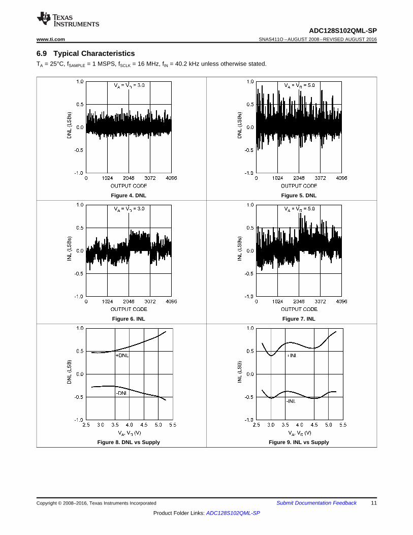
6.9 Typical CharacteristicsTA = 25°C, fSAMPLE = 1 MSPS, fSCLK = 16 MHz, fIN = 40.2 kHz unless otherwise stated.
Figure 4. DNL Figure 5. DNL
Figure 6. INL Figure 7. INL
Figure 8. DNL vs Supply Figure 9. INL vs Supply

12
ADC128S102QML-SPSNAS411O –AUGUST 2008–REVISED AUGUST 2016 www.ti.com
Product Folder Links: ADC128S102QML-SP
Submit Documentation Feedback Copyright © 2008–2016, Texas Instruments Incorporated
Typical Characteristics (continued)TA = 25°C, fSAMPLE = 1 MSPS, fSCLK = 16 MHz, fIN = 40.2 kHz unless otherwise stated.
Figure 10. SNR vs Supply Figure 11. THD vs Supply
Figure 12. ENOB vs Supply Figure 13. DNL vs SCLK Duty Cycle
Figure 14. INL vs SCLK Duty Cycle Figure 15. SNR vs SCLK Duty Cycle

13
ADC128S102QML-SPwww.ti.com SNAS411O –AUGUST 2008–REVISED AUGUST 2016
Product Folder Links: ADC128S102QML-SP
Submit Documentation FeedbackCopyright © 2008–2016, Texas Instruments Incorporated
Typical Characteristics (continued)TA = 25°C, fSAMPLE = 1 MSPS, fSCLK = 16 MHz, fIN = 40.2 kHz unless otherwise stated.
Figure 16. THD vs SCLK Duty Cycle Figure 17. ENOB vs SCLK Duty Cycle
Figure 18. DNL vs SCLK Figure 19. INL vs SCLK
Figure 20. DNL vs SCLK Figure 21. INL vs SCLK

14
ADC128S102QML-SPSNAS411O –AUGUST 2008–REVISED AUGUST 2016 www.ti.com
Product Folder Links: ADC128S102QML-SP
Submit Documentation Feedback Copyright © 2008–2016, Texas Instruments Incorporated
Typical Characteristics (continued)TA = 25°C, fSAMPLE = 1 MSPS, fSCLK = 16 MHz, fIN = 40.2 kHz unless otherwise stated.
Figure 22. SNR vs SCLK Figure 23. SNR vs SCLK
Figure 24. THD vs SCLK Figure 25. THD vs SCLK
Figure 26. ENOB vs SCLK Figure 27. ENOB vs SCLK

15
ADC128S102QML-SPwww.ti.com SNAS411O –AUGUST 2008–REVISED AUGUST 2016
Product Folder Links: ADC128S102QML-SP
Submit Documentation FeedbackCopyright © 2008–2016, Texas Instruments Incorporated
Typical Characteristics (continued)TA = 25°C, fSAMPLE = 1 MSPS, fSCLK = 16 MHz, fIN = 40.2 kHz unless otherwise stated.
Figure 28. ENOB vs Temperature Figure 29. DNL vs Temperature
Figure 30. INL vs Temperature Figure 31. SNR vs Temperature
Figure 32. THD vs Temperature Figure 33. Power Consumption vs SCLK

IN0
IN7
MUX T/H
ADC128S102
SCLK
VA
AGND
DGND
VD
CS
DIN
DOUT
CONTROL
LOGIC
12-BIT
SUCCESSIVE
APPROXIMATION
ADC
.
.
.
AGND
16
ADC128S102QML-SPSNAS411O –AUGUST 2008–REVISED AUGUST 2016 www.ti.com
Product Folder Links: ADC128S102QML-SP
Submit Documentation Feedback Copyright © 2008–2016, Texas Instruments Incorporated
7 Detailed Description
7.1 OverviewThe ADC128S102 is a successive-approximation analog-to-digital converter designed around a chargeredistribution digital-to-analog converter.
7.2 Functional Block Diagram
7.3 Feature Description
7.3.1 ADC128S102 Transfer FunctionThe output format of the ADC128S102 is straight binary. Code transitions occur midway between successiveinteger LSB values. The LSB width for the ADC128S102 is VA / 4096. The ideal transfer characteristic is shownin Figure 34. The transition from an output code of 0000 0000 0000 to a code of 0000 0000 0001 is at 1/2 LSB,or a voltage of VA / 8192. Other code transitions occur at steps of one LSB.

VIN
D1R1
C2
30 pF
VA
D2C1
3 pF
Conversion Phase - Switch Open
Track Phase - Switch Closed
| ||
0V+VA - 1.5LSB0.5LSB
ANALOG INPUT
1LSB = VA/4096AD
C C
OD
E111...111
111...110
111...000
011...111
000...010
000...001
000...000
17
ADC128S102QML-SPwww.ti.com SNAS411O –AUGUST 2008–REVISED AUGUST 2016
Product Folder Links: ADC128S102QML-SP
Submit Documentation FeedbackCopyright © 2008–2016, Texas Instruments Incorporated
Feature Description (continued)
Figure 34. Ideal Transfer Characteristic
7.3.2 Analog InputsAn equivalent circuit for one of the input channels of the ADC128S102 is shown in Figure 35. Diodes D1 and D2provide ESD protection for the analog inputs. The operating range for the analog inputs is 0 V to VA. Goingbeyond this range will cause the ESD diodes to conduct and result in erratic operation.
The capacitor C1 in Figure 35 has a typical value of 3 pF and is mainly the package pin capacitance. Resistor R1is the ON-resistance of the multiplexer and track or hold switch and is typically 500 Ω. Capacitor C2 is theADC128S102 sampling capacitor, and is typically 30 pF. The ADC128S102 will deliver best performance whendriven by a low-impedance source (less than 100 Ω). This is especially important when using the ADC128S102to sample dynamic signals. Also important when sampling dynamic signals is a band-pass or low-pass filterwhich reduces harmonics and noise in the input. These filters are often referred to as anti-aliasing filters.
Figure 35. Equivalent Input Circuit
7.3.3 Digital Inputs and OutputsThe digital inputs of the ADC128S102 (SCLK, CS, and DIN) have an operating range of 0 V to VA. The inputs arenot prone to latch-up and may be asserted before the digital supply (VD) without any risk. The digital output(DOUT) operating range is controlled by VD. The output high voltage is VD – 0.5 V (minimum) while the outputlow voltage is 0.4 V (maximum).

IN0
MUX
AGND
SAMPLINGCAPACITOR
SW1
-
+ CONTROLLOGIC
CHARGEREDISTRIBUTION
DAC
VA/2
SW2
IN7
18
ADC128S102QML-SPSNAS411O –AUGUST 2008–REVISED AUGUST 2016 www.ti.com
Product Folder Links: ADC128S102QML-SP
Submit Documentation Feedback Copyright © 2008–2016, Texas Instruments Incorporated
Feature Description (continued)7.3.4 Radiation EnvironmentsCareful consideration should be given to environmental conditions when using a product in a radiationenvironment.
7.3.4.1 Total Ionizing DoseRadiation hardness assured (RHA) products are those part numbers with a total ionizing dose (TID) level listed inthe Device Information table in the Description section. Testing and qualification of these products is done on awafer level according to MIL-STD-883G, Test Method 1019.7. Testing is done according to Condition A and theExtended room temperature anneal test described in section 3.11 for application environment dose rates lessthan 0.027 rad(Si)/s. Wafer level TID data is available with lot shipments.
7.3.4.2 Single Event Latch-Up and Functional InterruptOne-time single event latch-up (SEL) and single event functional interrupt (SEFI) testing was preformedaccording to EIA/JEDEC Standard, EIA/JEDEC57. The linear energy transfer threshold (LETth) shown inFeatures is the maximum LET tested. A test report is available upon request.
7.3.4.3 Single Event UpsetA report on single event upset (SEU) is available upon request.
7.4 Device Functional Modes
7.4.1 ADC128S102 OperationSimplified schematics of the ADC128S102 in both track and hold operation are shown in Figure 36 and Figure 37respectively. In Figure 36, the ADC128S102 is in track mode: switch SW1 connects the sampling capacitor toone of eight analog input channels through the multiplexer, and SW2 balances the comparator inputs. TheADC128S102 is in this state for the first three SCLK cycles after CS is brought low.
Figure 37 shows the ADC128S102 in hold mode: switch SW1 connects the sampling capacitor to ground,maintaining the sampled voltage, and switch SW2 unbalances the comparator. The control logic then instructsthe charge-redistribution DAC to add or subtract fixed amounts of charge to or from the sampling capacitor untilthe comparator is balanced. When the comparator is balanced, the digital word supplied to the DAC is the digitalrepresentation of the analog input voltage. The ADC128S102 is in this state for the last thirteen SCLK cyclesafter CS is brought low.
Figure 36. ADC128S102 in Track Mode

IN0
MUX
AGND
SAMPLING
CAPACITOR
SW1
-
+ CONTROL
LOGIC
CHARGE
REDISTRIBUTION
DAC
SW2
IN7
VA /2
19
ADC128S102QML-SPwww.ti.com SNAS411O –AUGUST 2008–REVISED AUGUST 2016
Product Folder Links: ADC128S102QML-SP
Submit Documentation FeedbackCopyright © 2008–2016, Texas Instruments Incorporated
Device Functional Modes (continued)
Figure 37. ADC128S102 in Hold Mode
7.5 Programming
7.5.1 Serial InterfaceAn operational timing diagram and a serial interface timing diagram for the ADC128S102 are shown in Figure 1to Figure 3. CS, chip select, initiates conversions and frames the serial data transfers. SCLK (serial clock)controls both the conversion process and the timing of serial data. DOUT is the serial data output pin, where aconversion result is sent as a serial data stream, MSB first. Data to be written to the ADC128S102's ControlRegister is placed on DIN, the serial data input pin. New data is written to DIN with each conversion.
A serial frame is initiated on the falling edge of CS and ends on the rising edge of CS. Each frame must containan integer multiple of 16 rising SCLK edges. The ADC's DOUT pin is in a high impedance state when CS is highand is active when CS is low. Note that CS is asynchronous. Thus, CS acts as an output enable. Similarly, SCLKis internally gated off when CS is brought high.
During the first 3 cycles of SCLK, the ADC is in the track mode, acquiring the input voltage. For the next 13SCLK cycles the conversion is accomplished and the data is clocked out. SCLK falling edges 1 through 4 clockout leading zeros while falling edges 5 through 16 clock out the conversion result, MSB first. If there is more thanone conversion in a frame (continuous conversion mode), the ADC will re-enter the track mode on the fallingedge of SCLK after the N*16th rising edge of SCLK and re-enter the hold/convert mode on the N×16+4th fallingedge of SCLK. "N" is an integer value.
The ADC128S102 enters track mode under three different conditions. In Figure 1, CS goes low with SCLK highand the ADC enters track mode on the first falling edge of SCLK. In the second condition, CS goes low withSCLK low. Under this condition, the ADC automatically enters track mode and the falling edge of CS is seen asthe first falling edge of SCLK. In the third condition, CS and SCLK go low simultaneously and the ADC enterstrack mode. While there is no timing restriction with respect to the falling edges of CS and SCLK, see Figure 3for setup and hold time requirements for the falling edge of CS with respect to the rising edge of SCLK.
During each conversion, data is clocked into a control register through the DIN pin on the first 8 rising edges ofSCLK after the fall of CS. The control register is loaded with data indicating the input channel to be converted onthe subsequent conversion (see Table 2, Table 3, and Table 4).
Although the ADC128S102 is able to acquire the input signal to full resolution in the first conversion immediatelyfollowing power-up, the first conversion result after power-up will be that of a randomly selected channel.Therefore, the user needs to incorporate a dummy conversion to set the required channel that will be used onthe subsequent conversion.

20
ADC128S102QML-SPSNAS411O –AUGUST 2008–REVISED AUGUST 2016 www.ti.com
Product Folder Links: ADC128S102QML-SP
Submit Documentation Feedback Copyright © 2008–2016, Texas Instruments Incorporated
Programming (continued)Table 2. Control Register Bits
BIT 7 (MSB) BIT 6 BIT 5 BIT 4 BIT 3 BIT 2 BIT 1 BIT 0DONTC DONTC ADD2 ADD1 ADD0 DONTC DONTC DONTC
Table 3. Control Register Bit DescriptionsBIT SYMBOL DESCRIPTION7, 6, 2, 1, 0 DONTC Don't care. The values of these bits do not affect the device.5 ADD2 These three bits determine which input channel will be sampled and converted at the next conversion cycle.
The mapping between codes and channels is shown in Table 4.4 ADD13 ADD0
Table 4. Input Channel SelectionADD2 ADD1 ADD0 INPUT CHANNEL
0 0 0 IN00 0 1 IN10 1 0 IN20 1 1 IN31 0 0 IN41 0 1 IN51 1 0 IN61 1 1 IN7

IN0
IN7
.
.
.MICROPROCESSOR
DSP
SCLK
CS
DIN
DOUTAGND
VAVD
ADC128S102
LP2950 5V
0.1 PF 1.0 PF0.1 PF 1 PF0.1 PF
DGND
1.0 PF
51:
22:INPUT
1 nF
21
ADC128S102QML-SPwww.ti.com SNAS411O –AUGUST 2008–REVISED AUGUST 2016
Product Folder Links: ADC128S102QML-SP
Submit Documentation FeedbackCopyright © 2008–2016, Texas Instruments Incorporated
8 Application and Implementation
NOTEInformation in the following applications sections is not part of the TI componentspecification, and TI does not warrant its accuracy or completeness. TI’s customers areresponsible for determining suitability of components for their purposes. Customers shouldvalidate and test their design implementation to confirm system functionality.
8.1 Application InformationThe ADC128S102 device is a low-power, eight-channel 12-bit ADC with ensured performance specifications from50 kSPS to 1 MSPS. It is appropriate to utilize the ADC128S102 at sample rates below 50 kSPS by powering thedevice down (de-asserting CSB) in between conversions. The Electrical Characteristics information highlights theclock frequency where the ADC’s performance is ensured. There is no limitation on periods of time for shutdownbetween conversions.
8.2 Typical ApplicationA typical application is shown in Figure 38. The split analog and digital supply pins are both powered in thisexample by the Texas Instruments LP2950-N low-dropout voltage regulator. The analog supply is bypassed witha capacitor network located close to the ADC128S102. The digital supply is separated from the analog supply byan isolation resistor and bypassed with additional capacitors. The ADC128S102 uses the analog supply (VA) asits reference voltage, so it is very important that VA be kept as clean as possible. Due to the low powerrequirements of the ADC128S102, it is also possible to use a precision reference as a power supply.
Figure 38. Typical Application Circuit
8.2.1 Design RequirementsA positive supply only data acquisition system capable of digitizing up to eight single-ended input signals rangingfrom 0 to 5 V with BW = 10 kHz and a throughput up to 500 kSPS. The ADC128S102 has to interface to an MCUwhose supply is set at 5 V. If it is necessary to interface with an MCU that operates at 3.3 V or lower, VA and VDwill need to be separated and care must be taken to ensure that VA is powered before VD.
8.2.2 Detailed Design ProcedureThe signal range requirement forces the design to use 5-V analog supply at VA, analog supply. This follows fromthe fact that VA is also a reference potential for the ADC. If the requirement of interfacing to the MCU changes to3.3-V, it will be necessary to change the VD supply voltage to 3.3 V. The maximum sampling rate of theADC128S102 when all channels (eight) are enabled is, Fs = FSCLK / (16 × 8).
Note that faster sampling rates can be achieved when fewer channels are sampled. Single channel can besampled at the maximum rate of Fs (single) = FSCLK / 16.

22
ADC128S102QML-SPSNAS411O –AUGUST 2008–REVISED AUGUST 2016 www.ti.com
Product Folder Links: ADC128S102QML-SP
Submit Documentation Feedback Copyright © 2008–2016, Texas Instruments Incorporated
Typical Application (continued)The VA and VD pins are separated by a 51-Ω resistor in order to minimize digital noise from corrupting theanalog reference input. If additional filtering is required, the resistor can be replaced by a ferrite bead, thusachieving a 2nd-order filter response. Further noise consideration could be given to the SPI interface, especiallywhen the master MCU is capable of producing fast rising edges on the digital bus signals. Inserting smallresistances in the digital signal path may help in reducing the ground bounce, and thus improve the overall noiseperformance of the system. Care should be taken when the signal source is capable of producing voltagesbeyond VA. In such instances, the internal ESD diodes may start conducting. The ESD diodes are not intendedas input signal clamps. To provide the desired clamping action use Schottky diodes.
8.2.3 Application Curve
Figure 39. ENOB vs Temperature

SNC N S
N S N S
ttP P P
t t t t= ´ + ´
+ +
23
ADC128S102QML-SPwww.ti.com SNAS411O –AUGUST 2008–REVISED AUGUST 2016
Product Folder Links: ADC128S102QML-SP
Submit Documentation FeedbackCopyright © 2008–2016, Texas Instruments Incorporated
9 Power Supply RecommendationsThere are three major power supply concerns with this product: power supply sequencing, power management,and the effect of digital supply noise on the analog supply.
9.1 Power Supply SequenceThe ADC128S102 is a dual-supply device. The two supply pins share ESD resources, so care must be exercisedto ensure that the power is applied in the correct sequence. To avoid turning on the ESD diodes, the digitalsupply (VD) cannot exceed the analog supply (VA) by more than 300 mV, during a conversion cycle. Therefore,VA must ramp up before or concurrently with VD.
9.2 Power ManagementThe ADC128S102 is fully powered-up whenever CS is low and fully powered-down whenever CS is high, withone exception. If operating in continuous conversion mode, the ADC128S102 automatically enters power-downmode between SCLK's 16th falling edge of a conversion and SCLK's 1st falling edge of the subsequentconversion (see Figure 1).
In continuous conversion mode, the ADC128S102 can perform multiple conversions back to back. Eachconversion requires 16 SCLK cycles and the ADC128S102 will perform conversions continuously as long as CSis held low. Continuous mode offers maximum throughput.
In burst mode, the user may trade off throughput for power consumption by performing fewer conversions perunit time. This means spending more time in power-down mode and less time in normal mode. By utilizing thistechnique, the user can achieve very low sample rates while still utilizing an SCLK frequency within the electricalspecifications. The Power Consumption versus SCLK curve in the Typical Characteristics shows the typicalpower consumption of the ADC128S102. To calculate the power consumption (PC), simply multiply the fraction oftime spent in the normal mode (tN) by the normal mode power consumption (PN), and add the fraction of timespent in shutdown mode (tS) multiplied by the shutdown mode power consumption (PS) as shown in Equation 1.
(1)
9.3 Power Supply Noise ConsiderationsThe charging of any output load capacitance requires current from the digital supply, VD. The current pulsesrequired from the supply to charge the output capacitance will cause voltage variations on the digital supply. Ifthese variations are large enough, they could degrade SNR and SINAD performance of the ADC. Furthermore, ifthe analog and digital supplies are tied directly together, the noise on the digital supply will be coupled directlyinto the analog supply, causing greater performance degradation than would noise on the digital supply alone.Similarly, discharging the output capacitance when the digital output goes from a logic high to a logic low willdump current into the die substrate, which is resistive. Load discharge currents will cause "ground bounce" noisein the substrate that will degrade noise performance if that current is large enough. The larger the outputcapacitance, the more current flows through the die substrate and the greater the noise coupled into the analogchannel.
The first solution to keeping digital noise out of the analog supply is to decouple the analog and digital suppliesfrom each other or use separate supplies for them. To keep noise out of the digital supply, keep the output loadcapacitance as small as practical. If the load capacitance is greater than 50 pF, use a 100-Ω series resistor atthe ADC output, located as close to the ADC output pin as practical. This will limit the charge and dischargecurrent of the output capacitance and improve noise performance. Because the series resistor and the loadcapacitance form a low frequency pole, verify signal integrity once the series resistor has been added.

CS
VA
AGND
IN0
IN1
IN2
IN3
IN4
SCLK
DOUT
DIN
VD
DGND
IN7
IN6
IN5
GROUND PLANE
VIA to GROUND PLANE
^/'/d>_^hWW>zZ/>
ANALOG
SUPPLY
RAIL
toMCU
to analog
signal sources
24
ADC128S102QML-SPSNAS411O –AUGUST 2008–REVISED AUGUST 2016 www.ti.com
Product Folder Links: ADC128S102QML-SP
Submit Documentation Feedback Copyright © 2008–2016, Texas Instruments Incorporated
10 Layout
10.1 Layout GuidelinesCapacitive coupling between the noisy digital circuitry and the sensitive analog circuitry can lead to poorperformance. The solution is to keep the analog circuitry separated from the digital circuitry and the clock line asshort as possible.
Digital circuits create substantial supply and ground current transients. The logic noise generated could havesignificant impact upon system noise performance. To avoid performance degradation of the ADC128S102 dueto supply noise, do not use the same supply for the ADC128S102 that is used for digital logic.
Generally, analog and digital lines should cross each other at 90° to avoid crosstalk. However, to maximizeaccuracy in high resolution systems, avoid crossing analog and digital lines altogether. It is important to keepclock lines as short as possible and isolated from ALL other lines, including other digital lines. In addition, theclock line should also be treated as a transmission line and be properly terminated.
The analog input should be isolated from noisy signal traces to avoid coupling of spurious signals into the input.Any external component (for example, a filter capacitor) connected between the converter's input pins andground or to the reference input pin and ground should be connected to a very clean point in the ground plane.
We recommend the use of a single, uniform ground plane and the use of split power planes. The power planesshould be located within the same board layer. All analog circuitry (input amplifiers, filters, referencecomponents, and so forth) should be placed over the analog power plane. All digital circuitry and I/O lines shouldbe placed over the digital power plane. Furthermore, all components in the reference circuitry and the inputsignal chain that are connected to ground should be connected together with short traces and enter the analogground plane at a single, quiet point.
10.2 Layout Example
Figure 40. Layout Diagram

25
ADC128S102QML-SPwww.ti.com SNAS411O –AUGUST 2008–REVISED AUGUST 2016
Product Folder Links: ADC128S102QML-SP
Submit Documentation FeedbackCopyright © 2008–2016, Texas Instruments Incorporated
11 Device and Documentation Support
11.1 Device Support
11.1.1 Development SupportFor related documentation, see the following:• 5962R07727• Radiation Report• MIL-STD-883G, Test Method 1019.7
11.1.2 Device Nomenclature
11.1.2.1 Specification DefinitionsACQUISITION TIME is the time required for the ADC to acquire the input voltage. During this time, the hold
capacitor is charged by the input voltage.
APERTURE DELAY is the time between the fourth falling edge of SCLK and the time when the input signal isinternally acquired or held for conversion.
CHANNEL-TO-CHANNEL ISOLATION is resistance to coupling of energy from one channel into anotherchannel.
CONVERSION TIME is the time required, after the input voltage is acquired, for the ADC to convert the inputvoltage to a digital word.
CROSSTALK is the coupling of energy from one channel into another channel. This is similar to Channel-to-Channel Isolation, except for the sign of the data.
DIFFERENTIAL NON-LINEARITY (DNL) is the measure of the maximum deviation from the ideal step size of 1LSB.
DUTY CYCLE is the ratio of the time that a repetitive digital waveform is high to the total time of one period. Thespecification here refers to the SCLK.
EFFECTIVE NUMBER OF BITS (ENOB, or EFFECTIVE BITS) is another method of specifying Signal-to-Noiseand Distortion or SINAD. ENOB is defined as (SINAD - 1.76) / 6.02 and says that the converter isequivalent to a perfect ADC of this (ENOB) number of bits.
FULL POWER BANDWIDTH is a measure of the frequency at which the reconstructed output fundamentaldrops 3 dB below its low frequency value for a full scale input.
GAIN ERROR is the deviation of the last code transition (111...110) to (111...111) from the ideal (VREF - 1.5 LSB),after adjusting for offset error.
INTEGRAL NON-LINEARITY (INL) is a measure of the deviation of each individual code from a line drawn fromnegative full scale (½ LSB below the first code transition) through positive full scale (½ LSB abovethe last code transition). The deviation of any given code from this straight line is measured fromthe center of that code value.
INTERMODULATION DISTORTION (IMD) is the creation of additional spectral components as a result of twosinusoidal frequencies being applied to an individual ADC input at the same time. It is defined asthe ratio of the power in either the second or the third order intermodulation products to the sum ofthe power in both of the original frequencies. Second order products are fa ± fb, where fa and fb arethe two sine wave input frequencies. Third order products are (2fa ± fb ) and (fa ± 2fb). IMD isusually expressed in dB.
MISSING CODES are those output codes that will never appear at the ADC outputs. The ADC128S102 isverified not to have any missing codes.
OFFSET ERROR is the deviation of the first code transition (000...000) to (000...001) from the ideal (that is, GND+ 0.5 LSB).
SIGNAL TO NOISE RATIO (SNR) is the ratio, expressed in dB, of the rms value of the input signal to the rmsvalue of the sum of all other spectral components below one-half the sampling frequency, not

2f1
2f10
2f2
10
A
A++AlogTHD = 20
26
ADC128S102QML-SPSNAS411O –AUGUST 2008–REVISED AUGUST 2016 www.ti.com
Product Folder Links: ADC128S102QML-SP
Submit Documentation Feedback Copyright © 2008–2016, Texas Instruments Incorporated
Device Support (continued)including harmonics or d.c.
SIGNAL TO NOISE PLUS DISTORTION (S/N+D or SINAD) Is the ratio, expressed in dB, of the rms value ofthe input signal to the rms value of all of the other spectral components below half the clockfrequency, including harmonics but excluding d.c.
SPURIOUS FREE DYNAMIC RANGE (SFDR) is the difference, expressed in dB, between the desired signalamplitude to the amplitude of the peak spurious spectral component, where a spurious spectralcomponent is any signal present in the output spectrum that is not present at the input and may ormay not be a harmonic.
THROUGHPUT TIME is the minimum time required between the start of two successive conversions. It is theacquisition time plus the conversion time.
TOTAL HARMONIC DISTORTION (THD) is the ratio, expressed in dBc, of the rms total of the first five harmoniccomponents at the output to the rms level of the input signal frequency as seen at the output. THDis calculated as:
where• Af1 is the RMS power of the input frequency at the output• Af2 through Af10 are the RMS power in the first 9 harmonic frequencies (2)
11.2 Receiving Notification of Documentation UpdatesTo receive notification of documentation updates, navigate to the device product folder on ti.com. In the upperright corner, click on Alert me to register and receive a weekly digest of any product information that haschanged. For change details, review the revision history included in any revised document.
11.3 Community ResourcesThe following links connect to TI community resources. Linked contents are provided "AS IS" by the respectivecontributors. They do not constitute TI specifications and do not necessarily reflect TI's views; see TI's Terms ofUse.
TI E2E™ Online Community TI's Engineer-to-Engineer (E2E) Community. Created to foster collaborationamong engineers. At e2e.ti.com, you can ask questions, share knowledge, explore ideas and helpsolve problems with fellow engineers.
Design Support TI's Design Support Quickly find helpful E2E forums along with design support tools andcontact information for technical support.
11.4 TrademarksMICROWIRE, E2E are trademarks of Texas Instruments.SPI, QSPI are trademarks of Motorola, Inc..All other trademarks are the property of their respective owners.
11.5 Electrostatic Discharge CautionThese devices have limited built-in ESD protection. The leads should be shorted together or the device placed in conductive foamduring storage or handling to prevent electrostatic damage to the MOS gates.
11.6 GlossarySLYZ022 — TI Glossary.
This glossary lists and explains terms, acronyms, and definitions.
27
ADC128S102QML-SPwww.ti.com SNAS411O –AUGUST 2008–REVISED AUGUST 2016
Product Folder Links: ADC128S102QML-SP
Submit Documentation FeedbackCopyright © 2008–2016, Texas Instruments Incorporated
12 Mechanical, Packaging, and Orderable InformationThe following pages include mechanical, packaging, and orderable information. This information is the mostcurrent data available for the designated devices. This data is subject to change without notice and revision ofthis document. For browser-based versions of this data sheet, refer to the left-hand navigation.
12.1 Engineering SamplesEngineering samples are available for order and are identified by the "MPR" in the orderable device name (seePackaging Information in the Addendum). Engineering (MPR) samples meet the performance specifications ofthe datasheet at room temperature only and have not received the full space production flow or testing.Engineering samples may be QCI rejects that failed tests that would not impact the performance at roomtemperature, such as radiation or reliability testing.

PACKAGE OPTION ADDENDUM
www.ti.com 25-Oct-2016
Addendum-Page 1
PACKAGING INFORMATION
Orderable Device Status(1)
Package Type PackageDrawing
Pins PackageQty
Eco Plan(2)
Lead/Ball Finish(6)
MSL Peak Temp(3)
Op Temp (°C) Device Marking(4/5)
Samples
ADC128S102 MDR ACTIVE DIESALE Y 0 20 Green (RoHS& no Sb/Br)
Call TI Level-1-NA-UNLIM -55 to 125
ADC128S102WGMPR ACTIVE CFP NAC 16 TBD Call TI Call TI 25 Only ADC128S102WGMPR ES ACOWGMPR ES >T
ADC128S102WGRQV ACTIVE CFP NAC 16 TBD Call TI Call TI -55 to 125 ADC128S102WGRQMLV Q5962R0722701VZA ACO01VZA >T
ADC128S102WRQV ACTIVE CFP NAD 16 TBD Call TI Call TI -55 to 125 ADC128S102WRQMLV Q5962R0722701VFA ACO01VFA >T
(1) The marketing status values are defined as follows:ACTIVE: Product device recommended for new designs.LIFEBUY: TI has announced that the device will be discontinued, and a lifetime-buy period is in effect.NRND: Not recommended for new designs. Device is in production to support existing customers, but TI does not recommend using this part in a new design.PREVIEW: Device has been announced but is not in production. Samples may or may not be available.OBSOLETE: TI has discontinued the production of the device.
(2) Eco Plan - The planned eco-friendly classification: Pb-Free (RoHS), Pb-Free (RoHS Exempt), or Green (RoHS & no Sb/Br) - please check http://www.ti.com/productcontent for the latest availabilityinformation and additional product content details.TBD: The Pb-Free/Green conversion plan has not been defined.Pb-Free (RoHS): TI's terms "Lead-Free" or "Pb-Free" mean semiconductor products that are compatible with the current RoHS requirements for all 6 substances, including the requirement thatlead not exceed 0.1% by weight in homogeneous materials. Where designed to be soldered at high temperatures, TI Pb-Free products are suitable for use in specified lead-free processes.Pb-Free (RoHS Exempt): This component has a RoHS exemption for either 1) lead-based flip-chip solder bumps used between the die and package, or 2) lead-based die adhesive used betweenthe die and leadframe. The component is otherwise considered Pb-Free (RoHS compatible) as defined above.Green (RoHS & no Sb/Br): TI defines "Green" to mean Pb-Free (RoHS compatible), and free of Bromine (Br) and Antimony (Sb) based flame retardants (Br or Sb do not exceed 0.1% by weightin homogeneous material)
(3) MSL, Peak Temp. - The Moisture Sensitivity Level rating according to the JEDEC industry standard classifications, and peak solder temperature.
(4) There may be additional marking, which relates to the logo, the lot trace code information, or the environmental category on the device.
PACKAGE OPTION ADDENDUM
www.ti.com 25-Oct-2016
Addendum-Page 2
(5) Multiple Device Markings will be inside parentheses. Only one Device Marking contained in parentheses and separated by a "~" will appear on a device. If a line is indented then it is a continuationof the previous line and the two combined represent the entire Device Marking for that device.
(6) Lead/Ball Finish - Orderable Devices may have multiple material finish options. Finish options are separated by a vertical ruled line. Lead/Ball Finish values may wrap to two lines if the finishvalue exceeds the maximum column width.
Important Information and Disclaimer:The information provided on this page represents TI's knowledge and belief as of the date that it is provided. TI bases its knowledge and belief on informationprovided by third parties, and makes no representation or warranty as to the accuracy of such information. Efforts are underway to better integrate information from third parties. TI has taken andcontinues to take reasonable steps to provide representative and accurate information but may not have conducted destructive testing or chemical analysis on incoming materials and chemicals.TI and TI suppliers consider certain information to be proprietary, and thus CAS numbers and other limited information may not be available for release.
In no event shall TI's liability arising out of such information exceed the total purchase price of the TI part(s) at issue in this document sold by TI to Customer on an annual basis.
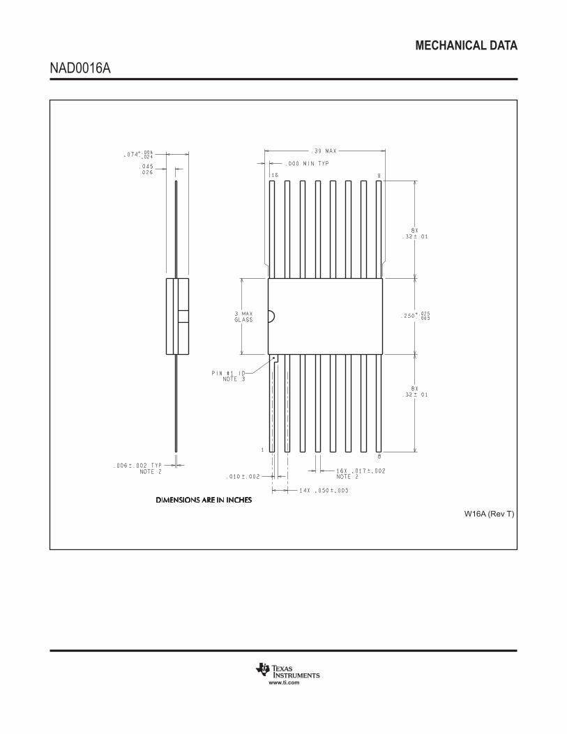
MECHANICAL DATA
NAD0016A
www.ti.com
W16A (Rev T)

MECHANICAL DATA
NAC0016A
www.ti.com
WG16A (RevG)

IMPORTANT NOTICE
Texas Instruments Incorporated and its subsidiaries (TI) reserve the right to make corrections, enhancements, improvements and otherchanges to its semiconductor products and services per JESD46, latest issue, and to discontinue any product or service per JESD48, latestissue. Buyers should obtain the latest relevant information before placing orders and should verify that such information is current andcomplete. All semiconductor products (also referred to herein as “components”) are sold subject to TI’s terms and conditions of salesupplied at the time of order acknowledgment.TI warrants performance of its components to the specifications applicable at the time of sale, in accordance with the warranty in TI’s termsand conditions of sale of semiconductor products. Testing and other quality control techniques are used to the extent TI deems necessaryto support this warranty. Except where mandated by applicable law, testing of all parameters of each component is not necessarilyperformed.TI assumes no liability for applications assistance or the design of Buyers’ products. Buyers are responsible for their products andapplications using TI components. To minimize the risks associated with Buyers’ products and applications, Buyers should provideadequate design and operating safeguards.TI does not warrant or represent that any license, either express or implied, is granted under any patent right, copyright, mask work right, orother intellectual property right relating to any combination, machine, or process in which TI components or services are used. Informationpublished by TI regarding third-party products or services does not constitute a license to use such products or services or a warranty orendorsement thereof. Use of such information may require a license from a third party under the patents or other intellectual property of thethird party, or a license from TI under the patents or other intellectual property of TI.Reproduction of significant portions of TI information in TI data books or data sheets is permissible only if reproduction is without alterationand is accompanied by all associated warranties, conditions, limitations, and notices. TI is not responsible or liable for such altereddocumentation. Information of third parties may be subject to additional restrictions.Resale of TI components or services with statements different from or beyond the parameters stated by TI for that component or servicevoids all express and any implied warranties for the associated TI component or service and is an unfair and deceptive business practice.TI is not responsible or liable for any such statements.Buyer acknowledges and agrees that it is solely responsible for compliance with all legal, regulatory and safety-related requirementsconcerning its products, and any use of TI components in its applications, notwithstanding any applications-related information or supportthat may be provided by TI. Buyer represents and agrees that it has all the necessary expertise to create and implement safeguards whichanticipate dangerous consequences of failures, monitor failures and their consequences, lessen the likelihood of failures that might causeharm and take appropriate remedial actions. Buyer will fully indemnify TI and its representatives against any damages arising out of the useof any TI components in safety-critical applications.In some cases, TI components may be promoted specifically to facilitate safety-related applications. With such components, TI’s goal is tohelp enable customers to design and create their own end-product solutions that meet applicable functional safety standards andrequirements. Nonetheless, such components are subject to these terms.No TI components are authorized for use in FDA Class III (or similar life-critical medical equipment) unless authorized officers of the partieshave executed a special agreement specifically governing such use.Only those TI components which TI has specifically designated as military grade or “enhanced plastic” are designed and intended for use inmilitary/aerospace applications or environments. Buyer acknowledges and agrees that any military or aerospace use of TI componentswhich have not been so designated is solely at the Buyer's risk, and that Buyer is solely responsible for compliance with all legal andregulatory requirements in connection with such use.TI has specifically designated certain components as meeting ISO/TS16949 requirements, mainly for automotive use. In any case of use ofnon-designated products, TI will not be responsible for any failure to meet ISO/TS16949.
Products ApplicationsAudio www.ti.com/audio Automotive and Transportation www.ti.com/automotiveAmplifiers amplifier.ti.com Communications and Telecom www.ti.com/communicationsData Converters dataconverter.ti.com Computers and Peripherals www.ti.com/computersDLP® Products www.dlp.com Consumer Electronics www.ti.com/consumer-appsDSP dsp.ti.com Energy and Lighting www.ti.com/energyClocks and Timers www.ti.com/clocks Industrial www.ti.com/industrialInterface interface.ti.com Medical www.ti.com/medicalLogic logic.ti.com Security www.ti.com/securityPower Mgmt power.ti.com Space, Avionics and Defense www.ti.com/space-avionics-defenseMicrocontrollers microcontroller.ti.com Video and Imaging www.ti.com/videoRFID www.ti-rfid.comOMAP Applications Processors www.ti.com/omap TI E2E Community e2e.ti.comWireless Connectivity www.ti.com/wirelessconnectivity
Mailing Address: Texas Instruments, Post Office Box 655303, Dallas, Texas 75265Copyright © 2016, Texas Instruments Incorporated