Embed Size (px)
Citation preview

Fabrication and Layout
Kenneth YunUC San Diego
Adapted from EE271 notes,Stanford University

Overviewn Semiconductor propertiesn How chips are maden Design rules for layoutn Reading
n Fabrication: W&E 3.1, 3.2.1, 3.3.1n Design Rules: W&E 3.4-3.4.3

What To Buildn Transistors
n nMOS and pMOS
n Wiresn Many levels of (real) metal wires
(aluminum and copper)n Need low resistance (high conductivity)
n Oxide insulators between metal layersn Contacts (hole in the oxide) between
adjacent layers
Siliconn Semiconductor
n Conductivity changed by adding impuritiesn Impurities, called dopants, create either n-
type or p-type regionsn Oxide is stable
n SiO2 (quarz or glass)n Great for sealing things from impuritiesn Can be selectively patternedn Etching can remove SiO2 without harming
Si
Dopingn Adding arsenic or phosphorous to
intrinsic silicon increases conductivityn By adding ‘free’ electronsn n-type since current is carried by
negatively charged particles (electrons)n Adding boron to intrinsic silicon
increases conductivityn By adding ‘free’ holesn p-type since current is carried by positively
charged “particles”
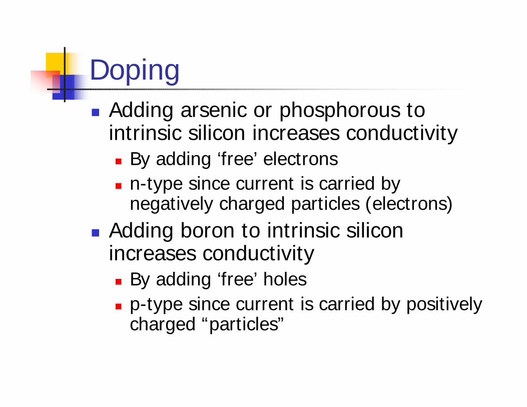
Dioden Junction between n-type and p-type
regions form a diode
I
V
n+
n
p+ p+

How To Build Transistorn Diffusion made by adding (diffusing)
impurities into siliconn n+ (p+) diffusion has lots of impurities
(dopants), so higher conductivityn p (n) regions lightly dopedn p region formed first; n+ doped over parts
of p regionn n+ dopant added after poly is down so
that poly blocks dopant
n+ n+
poly
p

Two Transistor Typesn CMOS requires two types of substrates
for isolation of transistorsn n-type for pMOSn p-type for nMOS
s d
g
crosssection
n+ n+p p+ p+n
Substrate = p Substrate = n
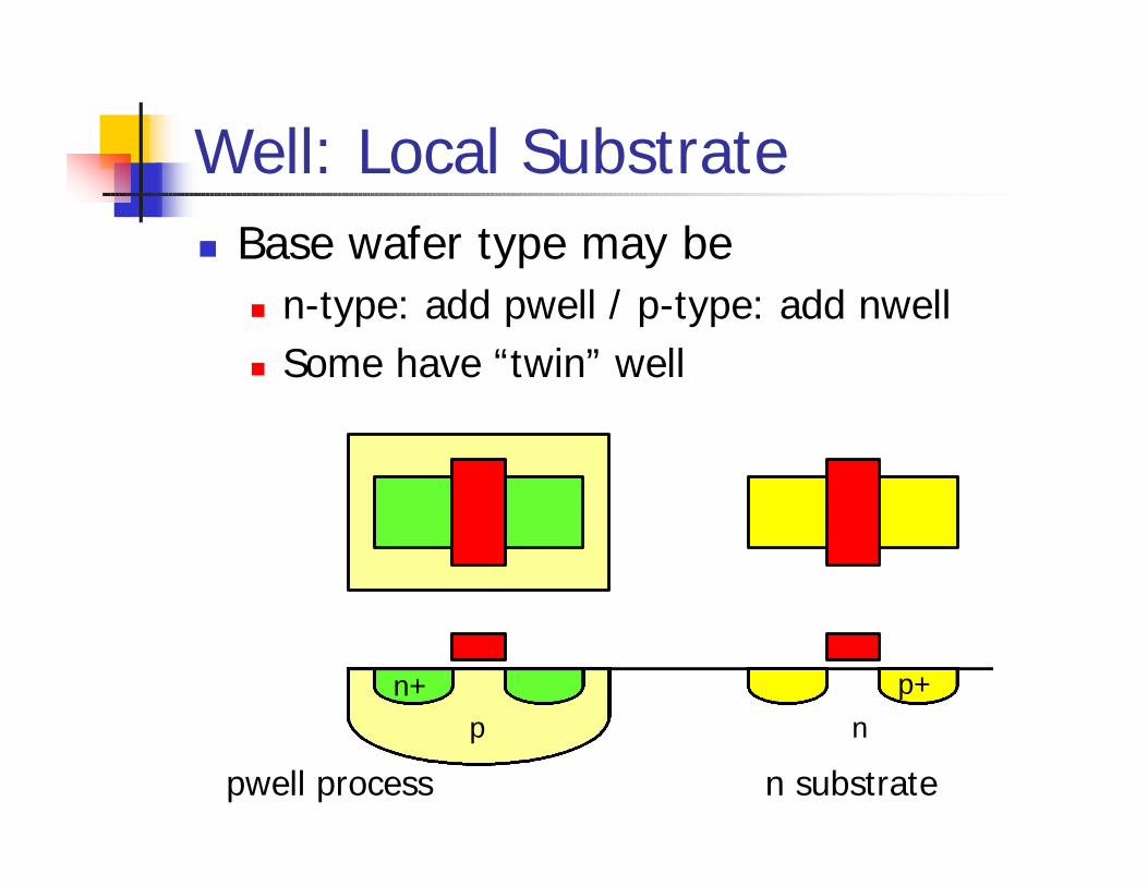
Well: Local Substraten Base wafer type may be
n n-type: add pwell / p-type: add nwelln Some have “twin” well
n+ p+p
pwell process n substrate
n

Well Requirementn Well must be tied to a power supply to
keep isolation diode reversed biasedn Using well contacts (ohmic connection to
the well)
n+ n+p p+ p+n
Tied to GND Tied to Vdd

Well Contactsn Formed by placing p+ doped region in
pwell (n+ region in nwell)n These regions make good electrical
contact to the well (ohmic, not diode)n Well potential equal to the diffusion
potential
n Need to have at least one well contact in each well

What’s On A Chip: Reviewn Transistors
n Require silicon substrate, wells, two types of diffusion, poly
n Wiresn Many levels of (real) metal wiresn Oxide insulator between metal layersn Contacts between adjacent layers

Fabrication
WafersProcessing
ProcessedWafer
Chips
Masks

Basic Fabrication Stepsn Transfer image of the design to wafer
(photolithography)n Create layers (diffusion/oxide/metal)
n Ion implant for diffusion; shoot impurities at silicon
n Deposition for oxide/metal; usually chemical vapor deposition (CVD)
n Grow for oxide; place silicon in oxidizing ambient

Basic Processing
Start with wafer at current step
Spin on a photoresist
Pattern photoresist with mask
Step specific processingetch, implant, etc...
Wash off resist

IC Fabricationn Repeat
n Create layer on wafern Put photo-sensitive material (resist) on top of
wafern Optically project image of pattern on watern Develop resistn Use resist as mask to prevent etch from reaching
layer below, when transferring pattern to layern Remove resist
n All die on wafer processed in parallel; for some chemical steps, many wafers processed in parallel

Photolithographyn To transfer pattern onto wafer, first need an
image to projectn Glass plate (mask) with image of pattern etched in
chrome generated from design databasen Mask = negative in photography
n Image optically projected onto wafer using “projection aligner”n projection aligner = enlarger in photography
n Mask allows printing on large number of wafersn Cost per wafer low, assuming lots of wafers
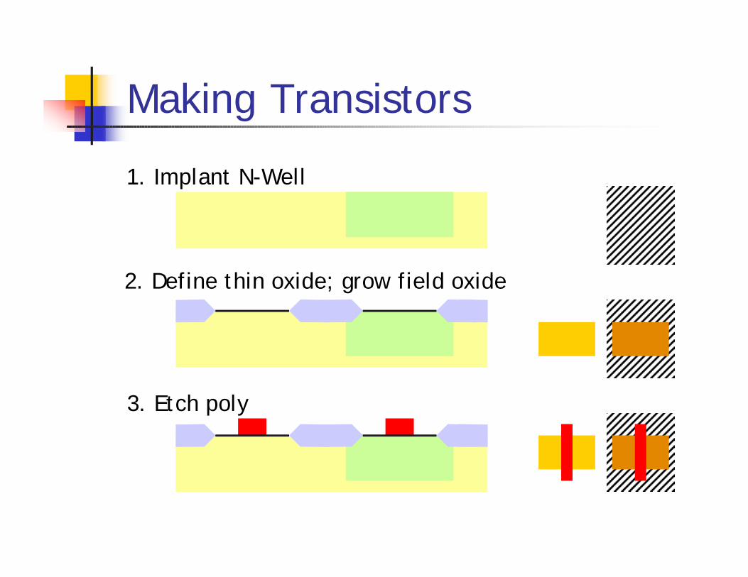
Making Transistors
1. Implant N-Well
2. Define thin oxide; grow field oxide
3. Etch poly
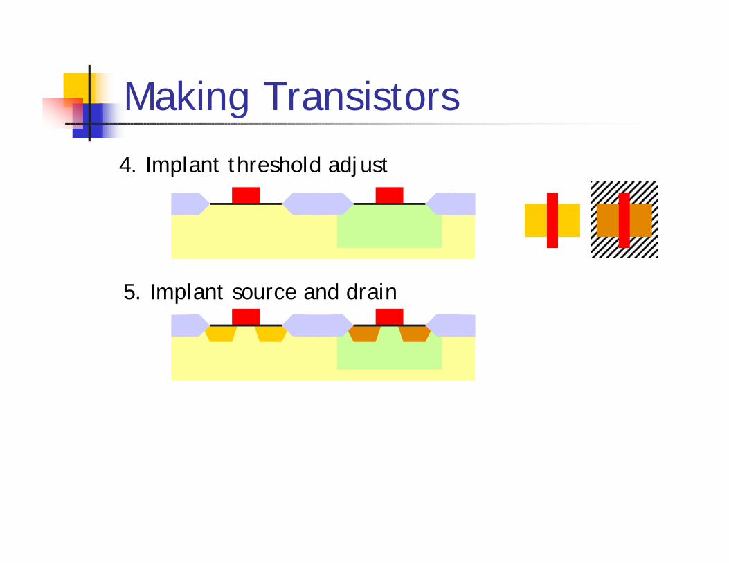
Making Transistors
4. Implant threshold adjust
5. Implant source and drain
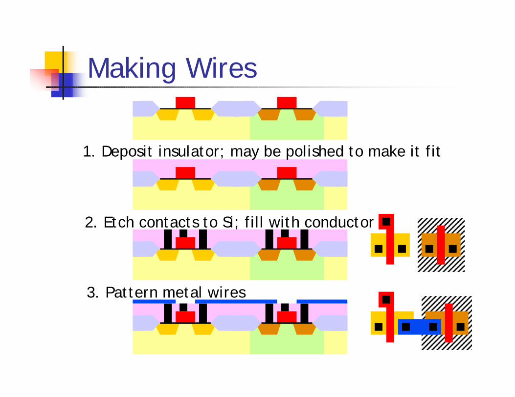
Making Wires
1. Deposit insulator; may be polished to make it fit
2. Etch contacts to Si; fill with conductor
3. Pattern metal wires
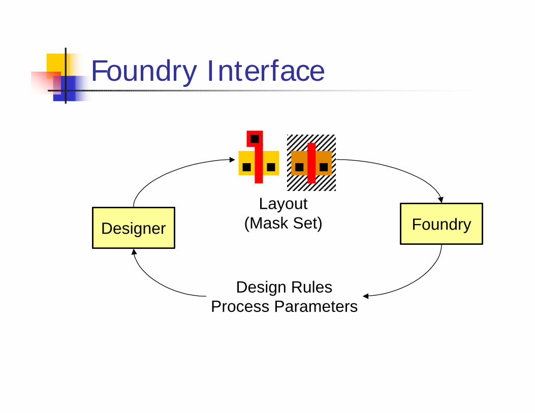
Foundry Interface
Designer FoundryLayout
(Mask Set)
Design RulesProcess Parameters

MAGIC MOSIS SCMOS Layers
n 4 types of diffusionn Normal (forms transistor)
n ndiffn pdiff
n Diffusion for well contactsn nohmicn pohmic
n Polyn Metal
n M1n M2
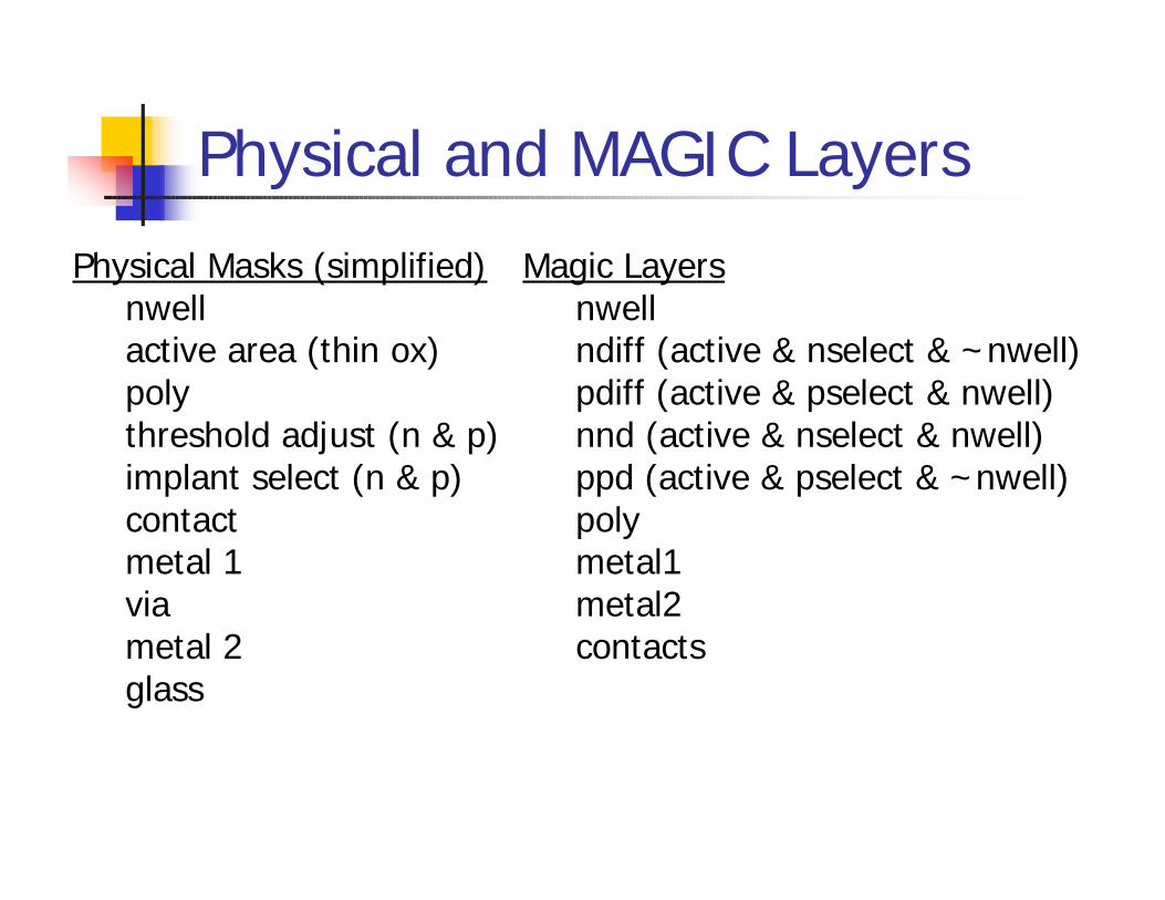
Physical and MAGIC Layers
Physical Masks (simplified)nwellactive area (thin ox)polythreshold adjust (n & p)implant select (n & p)contactmetal 1viametal 2glass
Magic Layersnwellndiff (active & nselect & ~nwell)pdiff (active & pselect & nwell)nnd (active & nselect & nwell)ppd (active & pselect & ~nwell)polymetal1metal2contacts

Layer Example

MAGIC Contacts
+ + =
ndc - ndiff to metal1
pdc - pdiff to metal1
ppc - ppd to metal1
nnc - nnd to metal1
pc - poly to metal1
via - metal1 to metal2

Contact Example

Fabrication Constraints On Layoutn Resolution constraints
n Smallest printable feature / smallest spacing that guarantees no short
n Depends on lithography and processing steps
n Resolution often depends on smoothness of surface
n Alignment/overlap constraintsn Need to align layers (like printing color
picture)
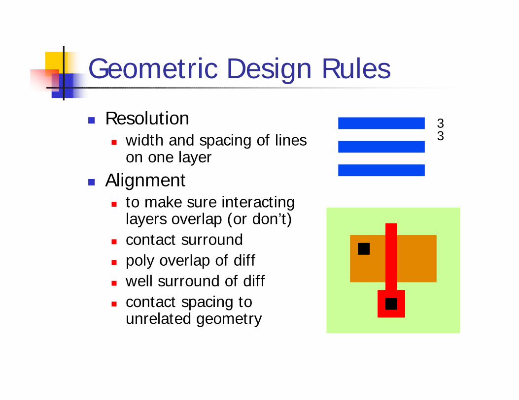
Geometric Design Rules
n Resolutionn width and spacing of lines
on one layer
n Alignmentn to make sure interacting
layers overlap (or don’t)n contact surroundn poly overlap of diffn well surround of diffn contact spacing to
unrelated geometry
33
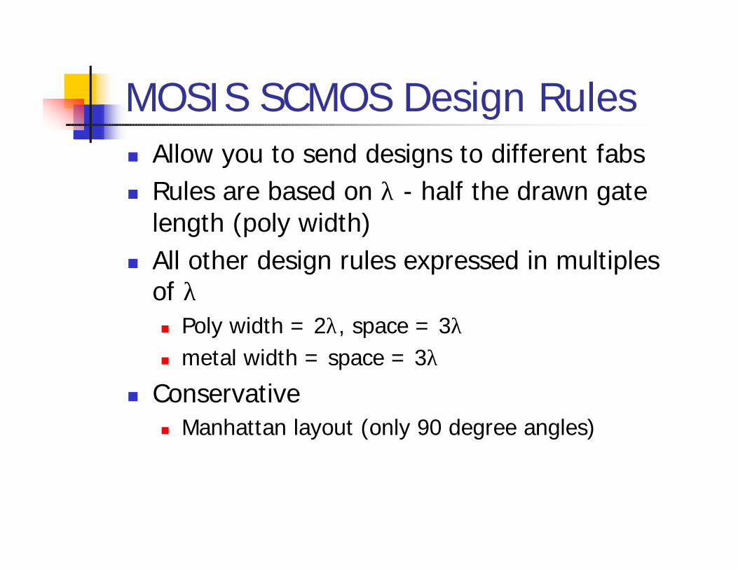
MOSIS SCMOS Design Rulesn Allow you to send designs to different fabsn Rules are based on λ - half the drawn gate
length (poly width)n All other design rules expressed in multiples
of λn Poly width = 2λ, space = 3λn metal width = space = 3λ
n Conservativen Manhattan layout (only 90 degree angles)

SCMOS Design Rule Highlightsn Resolution rules
Layer Width Spacepoly 2 3diff 3 3m1 3 3m2 3 4nwell 10 9cut 2 2via 2 3
cut/via surround 1poly overlap diff 2poly space to diff 1
Notes:Cut plus surround is 4Layout falls on 8λ grid
n Alignment rules

Pitchn Repeat distance between objects
n 8λ contacted transistor pitchn cut + poly width + 2 x cut-to-poly
n 6.5λ semi-contacted m1 pitchn (contact + width)/2 + spacing
n 7.5λ semi-contacted m2 pitchn (contact + width)/2 + spacing
n 7λ fully contacted m1 pitchn contact + spacing
n 8λ fully contacted m2 pitchn contact + spacing
8λ
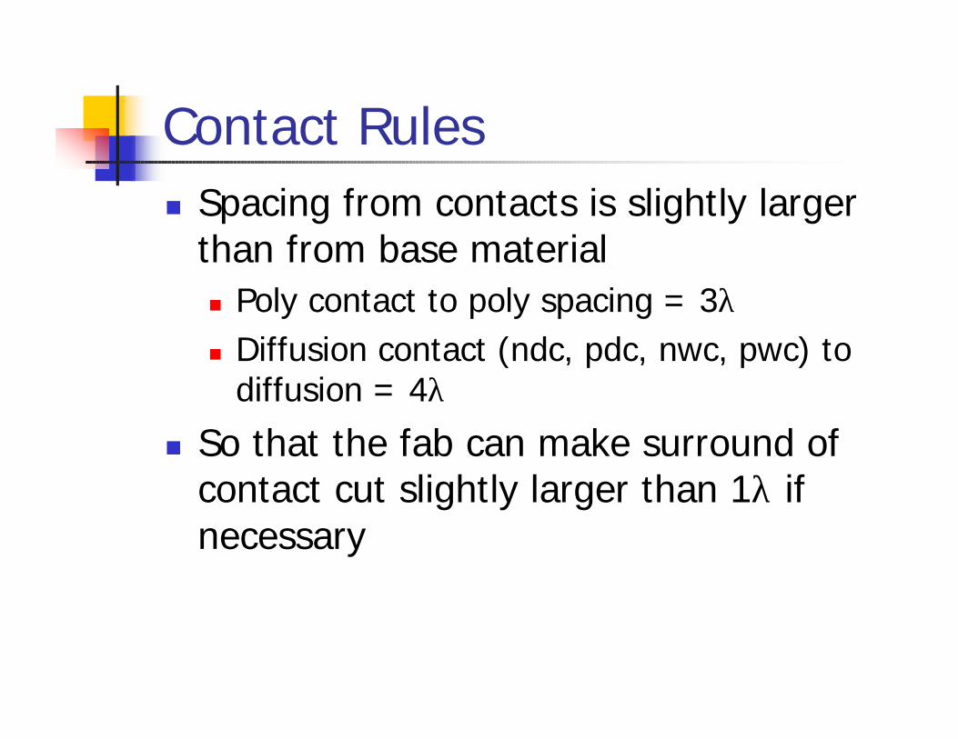
Contact Rulesn Spacing from contacts is slightly larger
than from base materialn Poly contact to poly spacing = 3λn Diffusion contact (ndc, pdc, nwc, pwc) to
diffusion = 4λ
n So that the fab can make surround of contact cut slightly larger than 1λ if necessary

Magic Number “8”
n Most of the important rules for estimating the size of stick diagram can be approximated by 8λ
M1 w/c = 7
M2 w/c = 8
poly w/dc = 8
diff w/c = 8
8
poly w/c = 7
(diff width =4)

Stick Diagramsn Like a layout
n Basic topology of the circuitn Relative positions of objects roughly
correct
n Butn Wires have no widthn Size of objects not to scalen Missing wires can be squeezed in between
two wires

Layout Issuesn Two types of diffusion
n ndiffn poly crossing ndiff makes nMOS transistor
n pdiffn poly crossing pdiff makes pMOS transistor
n Cannot directly connect ndiff and pdiffn must connect ndiff to metal and metal to pdiff
n Cannot get ndiff too close to pdiff because of wellsn large spacing rule between ndiff and pdiffn need to group nMOS transistors together and pMOS
transistors together
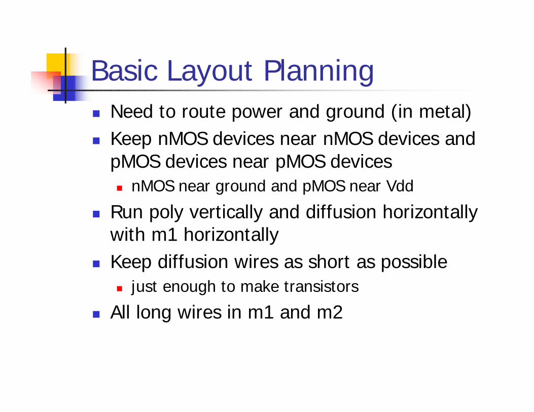
Basic Layout Planningn Need to route power and ground (in metal)n Keep nMOS devices near nMOS devices and
pMOS devices near pMOS devicesn nMOS near ground and pMOS near Vdd
n Run poly vertically and diffusion horizontally with m1 horizontally
n Keep diffusion wires as short as possiblen just enough to make transistors
n All long wires in m1 and m2

Typical Cell Layout Plann Parity
n Inverter
Vdd
Gnd