Embed Size (px)
Citation preview

7/22/2019 AD5933 datasheet
http://slidepdf.com/reader/full/ad5933-datasheet 1/40
1 MSPS, 12-Bit Impedance
Converter, Network Analyzer
Data Sheet AD5933
Rev. E Document FeedbackInformation furnished by Analog Devices is believed to be accurate and reliable. However, noresponsibility is assumed by Analog Devices for its use, nor for any infringements of patents or otherrights of third parties that may result from its use. Specifications subject to change without notice. Nolicense is granted by implication or otherwise under any patent or patent rights of Analog Devices.Trademarks and registered trademarks are the property of their respective owners.
One Technology Way, P.O. Box 9106, Norwood, MA 02062-9106, U.S.ATel: 781.329.4700 ©2005–2013 Analog Devices, Inc. All rights reservedTechnical Support www.analog.com
FEATURES
Programmable output peak-to-peak excitation voltageto a maximum frequency of 100 kHz
Programmable frequency sweep capability with
serial I2C interface
Frequency resolution of 27 bits (<0.1 Hz)
Impedance measurement range from 1 kΩ to 10 MΩ
Capable of measuring of 100 Ω to 1 kΩ with additional
circuitry
Internal temperature sensor (±2°C)
Internal system clock option
Phase measurement capability
System accuracy of 0.5%
2.7 V to 5.5 V power supply operation
Temperature range: −40°C to +125°C
16-lead SSOP package
Qualified for automotive applications
APPLICATIONS
Electrochemical analysis
Bioelectrical impedance analysis
Impedance spectroscopy
Complex impedance measurement
Corrosion monitoring and protection equipment
Biomedical and automotive sensors
Proximity sensing
Nondestructive testing
Material property analysis
Fuel/battery cell condition monitoring
GENERAL DESCRIPTION
The AD5933 is a high precision impedance converter system
solution that combines an on-board frequency generator with
a 12-bit, 1 MSPS, analog-to-digital converter (ADC). The
frequency generator allows an external complex impedance to
be excited with a known frequency. The response signal from
the impedance is sampled by the on-board ADC and a discrete
Fourier transform (DFT) is processed by an on-board DSP
engine. The DFT algorithm returns a real (R) and imaginary (I)
data-word at each output frequency.
Once calibrated, the magnitude of the impedance and relative
phase of the impedance at each frequency point along the sweep
is easily calculated. This is done off chip using the real and
imaginary register contents, which can be read from the serialI2C interface.
A similar device, also available from Analog Devices, Inc., is the
AD5934, a 2.7 V to 5.5 V, 250 kSPS, 12-bit impedance converter
with an internal temperature sensor and is packaged in a 16-
lead SSOP.
FUNCTIONAL BLOCK DIAGRAM
VDD/2
DAC
Z(ω)
SCL
SDA
DVDDAVDDMCLK
AGND DGND
ROUT VOUT
AD5933
RFB
VIN
0 5 3 2 4 - 0 0 1
1024-POINT DFT
I2CINTERFACE
IMAGINARYREGISTERREALREGISTER
OSCILLATOR
DDSCORE
(27 BITS)
TEMPERATURESENSOR
ADC(12 BITS)
LPFGAIN
Figure 1.

7/22/2019 AD5933 datasheet
http://slidepdf.com/reader/full/ad5933-datasheet 2/40
AD5933 Data Sheet
Rev. E | Page 2 of 40
TABLE OF CONTENTSFeatures .............................................................................................. 1 Applications ....................................................................................... 1
General Description ......................................................................... 1
Functional Block Diagram .............................................................. 1 Revision History ............................................................................... 3 Specifications ..................................................................................... 4
I2C Serial Interface Timing Characteristics .............................. 6
Absolute Maximum Ratings ............................................................ 7 ESD Caution .................................................................................. 7
Pin Configuration and Descriptions .............................................. 8 Typical Performance Characteristics ............................................. 9
Terminology .................................................................................... 12 System Description ......................................................................... 13
Transmit Stage ............................................................................. 14 Frequency Sweep Command Sequence ................................... 15 Receive Stage ............................................................................... 15
DFT Operation ........................................................................... 15 System Clock ............................................................................... 16
Temperature Sensor ................................................................... 16 Temperature Conversion Details .............................................. 16 Temperature Value Register ...................................................... 16
Temperature Conversion Formula ........................................... 16
Impedance Calculation .................................................................. 17 Magnitude Calculation .............................................................. 17 Gain Factor Calculation ............................................................ 17
Impedance Calculation Using Gain Factor ............................. 17 Gain Factor Variation with Frequency .................................... 17 Two-Point Calibration ............................................................... 18
Two-Point Gain Factor Calculation ......................................... 18 Gain Factor Setup Configuration ............................................. 18
Gain Factor Recalculation ......................................................... 18 Gain Factor Temperature Variation ......................................... 19
Impedance Error ......................................................................... 19 Measuring the Phase Across an Impedance ........................... 19
Performing a Frequency Sweep .................................................... 22
Register Map ................................................................................... 23 Control Register (Register Address 0x80, Register Address0x81) ............................................................................................. 23
Start Frequency Register (Register Address 0x82, RegisterAddress 0x83, Register Address 0x84) .................................... 24 Frequency Increment Register (Register Address 0x85,Register Address 0x86, Register Address 0x87) ..................... 25
Number of Increments Register (Register Address 0x88,Register Address 0x89) .............................................................. 25 Number of Settling Time Cycles Register (Register Address0x8A, Register Address 0x8B) ................................................. 25 Status Register (Register Address 0x8F) .................................. 26 Temperature Data Register (16 Bits—Register Address 0x92,Register Address 0x93) .............................................................. 26
Real and Imaginary Data Registers (16 Bits—RegisterAddress 0x94, Register Address 0x95, Register Address 0x96,Register Address 0x97) .............................................................. 26
Serial Bus Interface ......................................................................... 27 General I2C Timing .................................................................... 27 Writing/Reading to the AD5933 .............................................. 28
Block Write .................................................................................. 28
Read Operations ......................................................................... 29
Typical Applications ....................................................................... 30 Measuring Small Impedances ................................................... 30
Biomedical: Noninvasive Blood Impedance Measurement .. 32 Sensor/Complex Impedance Measurement ............................ 32 Electro-Impedance Spectroscopy ............................................. 33
Layout and Configuration ............................................................. 34 Power Supply Bypassing and Grounding ................................ 34
Evaluation Board ............................................................................ 35
Using the Evaluation Board ...................................................... 35 Prototyping Area ........................................................................ 35
Crystal Oscillator (XO) vs. External Clock ............................. 35 Schematics ................................................................................... 36
Outline Dimensions ....................................................................... 40 Ordering Guide .......................................................................... 40
Automotive Products ................................................................. 40

7/22/2019 AD5933 datasheet
http://slidepdf.com/reader/full/ad5933-datasheet 3/40
Data Sheet AD5933
Rev. E | Page 3 of 40
REVISION HISTORY
5/13—Rev. D to Rev. E
Added Automotive Information (Throughout) ............................ 1Changed Sampling Rate from 250 kSPS to 1 MSPS ..................... 5Changes to Table 7 .......................................................................... 21
Deleted Choosing a Reference for the AD5933 Section ............ 34Changes to Ordering Guide ........................................................... 40
12/11—Rev. C to Rev. D
Changes to Impedance Error Section ........................................... 19Removed Figure 26 and Figure 27;Renumbered Sequentially .............................................................. 19Removed Figure 28, Figure 29, Figure 30, Figure 31 .................. 20Changes to Figure 39 ...................................................................... 37Changes to Figure 40 ...................................................................... 38Changes to Figure 41 ...................................................................... 39Changes to Figure 42 ...................................................................... 40
8/10—Rev. B to Rev. C
Changes to Impedance Error Section ........................................... 19Changes to Figure 45 ...................................................................... 38Changes to U4 Description in Table 19 ........................................ 42
2/10—Rev. A to Rev. B
Changes to General Description ..................................................... 1
5/08—Rev. 0 to Rev. A
Changes to Layout .............................................................. UniversaChanges to Figure 1 .......................................................................... 1Changes to Table 1 ............................................................................ 4Changes to Figure 17 ...................................................................... 13Changes to System Description Section....................................... 13Changes to Figure 19 ...................................................................... 14Changes to Figure 24 ...................................................................... 18Changes to Impedance Error Section ........................................... 19Added Measuring the Phase Across an Impedance Section ..... 21Changes to Register Map Section ................................................. 24Added Measuring Small Impedances Section ............................. 31Changes to Table 18 ........................................................................ 35Added Evaluation Board Section .................................................. 37
Changes to Ordering Guide ........................................................... 439/05—Revision 0: Initial Version

7/22/2019 AD5933 datasheet
http://slidepdf.com/reader/full/ad5933-datasheet 4/40
AD5933 Data Sheet
Rev. E | Page 4 of 40
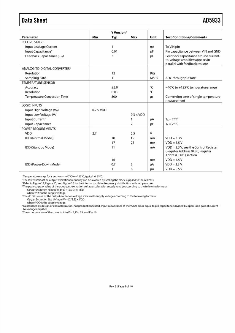
SPECIFICATIONS
VDD = 3.3 V, MCLK = 16.776 MHz, 2 V p-p output excitation voltage @ 30 kHz, 200 kΩ connected between Pin 5 and Pin 6; feedbackresistor = 200 kΩ connected between Pin 4 and Pin 5; PGA gain = ×1, unless otherwise noted.
Table 1.
ParameterY Version1
Unit Test Conditions/CommentsMin Typ Max
SYSTEM
Impedance Range 1 K 10 M Ω 100 Ω to 1 kΩ requires extra buffercircuitry, see the Measuring SmallImpedances section
Total System Accuracy 0.5 % 2 V p-p output excitation voltage at30 kHz, 200 kΩ connected betweenPin 5 and Pin 6
System Impedance Error Drift 30 ppm/°C
TRANSMIT STAGE
Output Frequency Range2 1 100 kHz
Output Frequency Resolution 0.1 Hz <0.1 Hz resolution achievable using
DDS techniquesMCLK Frequency 16.776 MHz Maximum system clock frequency
Internal Oscillator Frequency3 16.776 MHz Frequency of internal clock
Internal Oscillator Temperature Coefficient 30 ppm/°C
TRANSMIT OUTPUT VOLTAGE
Range 1
AC Output Excitation Voltage4 1.98 V p-p See Figure 4 for output voltagedistribution
DC Bias5 1.48 V DC bias of the ac excitation signal;see Figure 5
DC Output Impedance 200 Ω TA = 25°C
Short-Circuit Current to Ground at VOUT ±5.8 mA TA = 25°C
Range 2
AC Output Excitation Voltage4 0.97 V p-p See Figure 6DC Bias5 0.76 V DC bias of output excitation signal;
see Figure 7
DC Output Impedance 2.4 kΩ
Short-Circuit Current to Ground at VOUT ±0.25 mA
Range 3
AC Output Excitation Voltage4 0.383 V p-p See Figure 8
DC Bias5 0.31 V DC bias of output excitation signal;see Figure 9
DC Output Impedance 1 kΩ
Short-Circuit Current to Ground at VOUT ±0.20 mA
Range 4
AC Output Excitation Voltage4 0.198 V p-p See Figure 10
DC Bias5 0.173 V DC bias of output excitation signal.See Figure 11
DC Output Impedance 600 Ω
Short-Circuit Current to Ground at VOUT ±0.15 mA
SYSTEM AC CHARACTERISTICS
Signal-to-Noise Ratio 60 dB
Total Harmonic Distortion −52 dB
Spurious-Free Dynamic Range
Wide Band (0 MHz to 1 MHz) −56 dB
Narrow Band (±5 kHz) −85 dB
7/22/2019 AD5933 datasheet
http://slidepdf.com/reader/full/ad5933-datasheet 5/40
Data Sheet AD5933
Rev. E | Page 5 of 40
Parameter
Y Version1
Unit Test Conditions/CommentsMin Typ Max
RECEIVE STAGE
Input Leakage Current 1 nA To VIN pin
Input Capacitance6 0.01 pF Pin capacitance between VIN and GND
Feedback Capacitance (CFB) 3 pF Feedback capacitance around currentto-voltage amplifier; appears inparallel with feedback resistor
ANALOG-TO-DIGITAL CONVERTER6
Resolution 12 Bits
Sampling Rate 1 MSPS ADC throughput rate
TEMPERATURE SENSOR
Accuracy ±2.0 °C −40°C to +125°C temperature range
Resolution 0.03 °C
Temperature Conversion Time 800 μs Conversion time of single temperaturemeasurement
LOGIC INPUTS
Input High Voltage (VIH) 0.7 × VDD
Input Low Voltage (VIL) 0.3 × VDDInput Current7 1 µA TA = 25°C
Input Capacitance 7 pF TA = 25°C
POWER REQUIREMENTS
VDD 2.7 5.5 V
IDD (Normal Mode ) 10 15 mA VDD = 3.3 V
17 25 mA VDD = 5.5 V
IDD (Standby Mode) 11 mA VDD = 3.3 V; see the Control Register(Register Address 0X80, RegisterAddress 0X81) section
16 mA VDD = 5.5 V
IDD (Power-Down Mode) 0.7 5 µA VDD = 3.3 V
1 8 µA VDD = 5.5 V
1 Temperature range for Y version = −40°C to +125°C, typical at 25°C.2 The lower limit of the output excitation frequency can be lowered by scaling the clock supplied to the AD5933.3 Refer to Figure 14, Figure 15, and Figure 16 for the internal oscillator frequency distribution with temperature.4 The peak-to-peak value of the ac output excitation voltage scales with supply voltage according to the following formula:
Output Excitation Voltage (V p-p) = [2/3.3] × VDD where VDD is the supply voltage.
5 The dc bias value of the output excitation voltage scales with supply voltage according to the following formula:Output Excitation Bias Voltage (V) = [2/3.3] × VDD where VDD is the supply voltage.
6 Guaranteed by design or characterization, not production tested. Input capacitance at the VOUT pin is equal to pin capacitance divided by open-loop gain of current-to-voltage amplifier.
7 The accumulation of the currents into Pin 8, Pin 15, and Pin 16.
7/22/2019 AD5933 datasheet
http://slidepdf.com/reader/full/ad5933-datasheet 6/40
AD5933 Data Sheet
Rev. E | Page 6 of 40
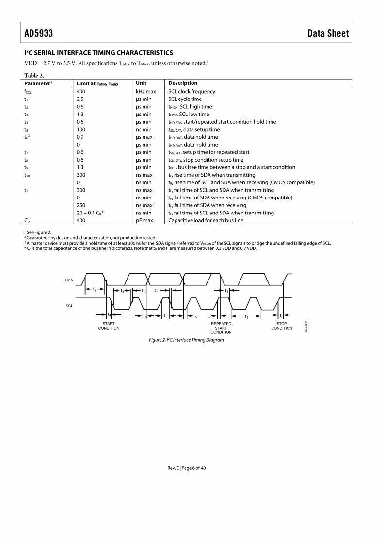
I2C SERIAL INTERFACE TIMING CHARACTERISTICS
VDD = 2.7 V to 5.5 V. All specifications TMIN to TMAX, unless otherwise noted.1
Table 2.
Parameter2 Limit at TMIN, TMAX Unit Description
f SCL 400 kHz max SCL clock frequency
t1 2.5 µs min SCL cycle time
t2 0.6 µs min tHIGH, SCL high time
t3 1.3 µs min tLOW, SCL low time
t4 0.6 µs min tHD, STA, start/repeated start condition hold time
t5 100 ns min tSU, DAT, data setup time
t63 0.9 µs max tHD, DAT, data hold time
0 µs min tHD, DAT, data hold time
t7 0.6 µs min tSU, STA, setup time for repeated start
t8 0.6 µs min tSU, STO, stop condition setup time
t9 1.3 µs min tBUF, bus free time between a stop and a start condition
t10 300 ns max tF, rise time of SDA when transmitting
0 ns min tR, rise time of SCL and SDA when receiving (CMOS compatible)
t11 300 ns max tF, fall time of SCL and SDA when transmitting0 ns min tF, fall time of SDA when receiving (CMOS compatible)
250 ns max tF, fall time of SDA when receiving
20 + 0.1 Cb4 ns min tF, fall time of SCL and SDA when transmitting
Cb 400 pF max Capacitive load for each bus line
1 See Figure 2.2 Guaranteed by design and characterization, not production tested.3 A master device must provide a hold time of at least 300 ns for the SDA signal (referred to V IH MIN of the SCL signal) to bridge the undefined falling edge of SCL.4 Cb is the total capacitance of one bus line in picofarads. Note that tR and tF are measured between 0.3 VDD and 0.7 VDD.
SCL
SDA
t9 t3 t10 t11 t4
t4 t6 t2 t5 t7 t8t1
0 5 3 2 4 - 0 0 2
START
CONDITION
REPEATED
START
CONDITION
STOP
CONDITION
Figure 2. I 2C Interface Timing Diagram
7/22/2019 AD5933 datasheet
http://slidepdf.com/reader/full/ad5933-datasheet 7/40
Data Sheet AD5933
Rev. E | Page 7 of 40
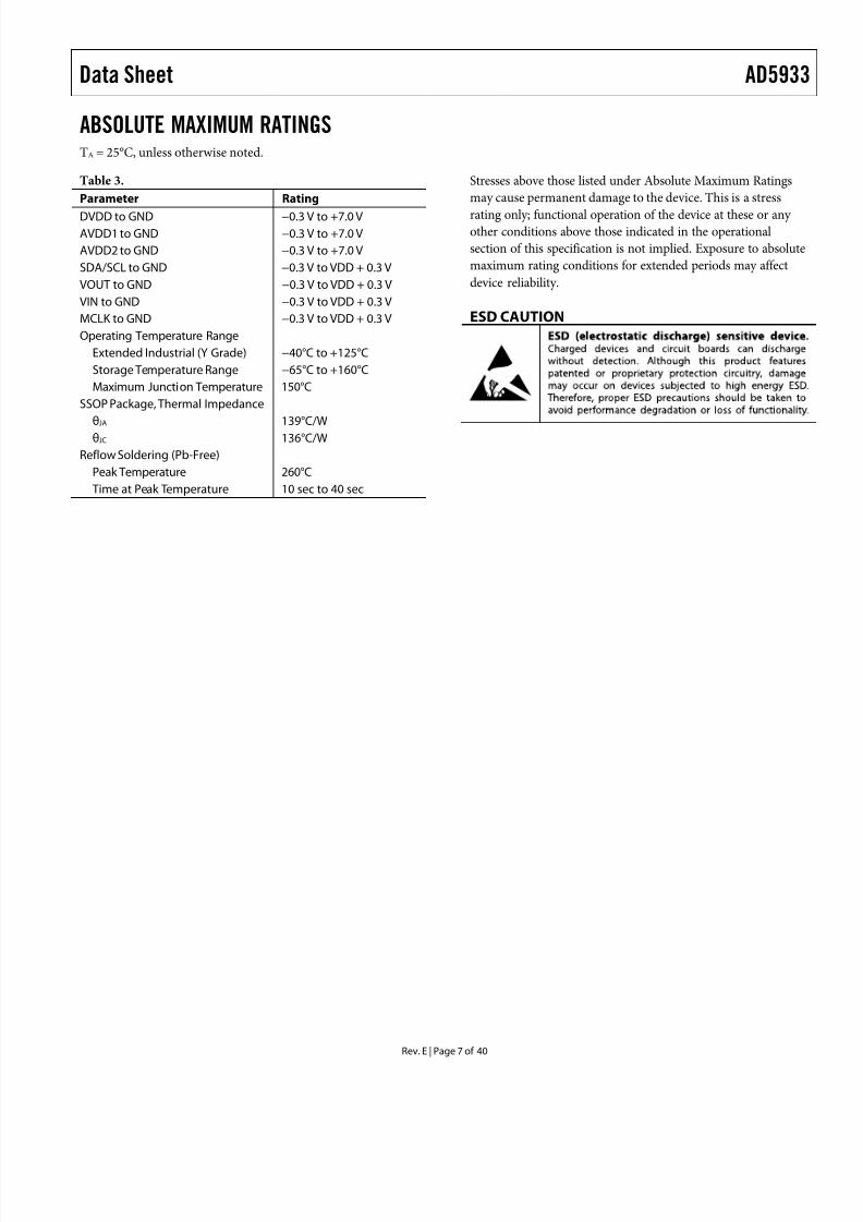
ABSOLUTE MAXIMUM RATINGS
TA = 25°C, unless otherwise noted.
Table 3.
Parameter Rating
DVDD to GND −0.3 V to +7.0 VAVDD1 to GND −0.3 V to +7.0 V
AVDD2 to GND −0.3 V to +7.0 V
SDA/SCL to GND −0.3 V to VDD + 0.3 V
VOUT to GND −0.3 V to VDD + 0.3 V
VIN to GND −0.3 V to VDD + 0.3 V
MCLK to GND −0.3 V to VDD + 0.3 V
Operating Temperature Range
Extended Industrial (Y Grade) −40°C to +125°C
Storage Temperature Range −65°C to +160°C
Maximum Junction Temperature 150°C
SSOP Package, Thermal Impedance
θJA 139°C/WθJC 136°C/W
Reflow Soldering (Pb-Free)
Peak Temperature 260°C
Time at Peak Temperature 10 sec to 40 sec
Stresses above those listed under Absolute Maximum Ratingsmay cause permanent damage to the device. This is a stress
rating only; functional operation of the device at these or anyother conditions above those indicated in the operationalsection of this specification is not implied. Exposure to absolutemaximum rating conditions for extended periods may affectdevice reliability.
ESD CAUTION

7/22/2019 AD5933 datasheet
http://slidepdf.com/reader/full/ad5933-datasheet 8/40
AD5933 Data Sheet
Rev. E | Page 8 of 40
PIN CONFIGURATION AND DESCRIPTIONS
NC 1
NC 2
NC 3
RFB 4
SCL16
SDA15
AGND214
AGND113
VIN 5
VOUT 6
NC 7
DGND12
AVDD211
AVDD110
MCLK 8 DVDD9
NC = NO CONNECT
AD5933TOP VIEW
(Not to Scale)
0 5 3 2 4 - 0 0 3
IT IS RECOMMENDEDTO TIE ALL SUPPLYCONNECTIONS (PIN 9, PIN 10, AND PIN 11)
AND RUN FROM A SINGLE SUPPLY BETWEEN
2.7VAND 5.5V. IT IS ALSO RECOMMENDED TO
CONNECT ALL GROUND SIGNALS TOGETHER
(PIN 12, PIN 13, AND PIN 14).
NOTES:1.
Figure 3. Pin Configuration
Table 4. Pin Function Descriptions
Pin No. Mnemonic Description
1, 2, 3, 7 NC No Connect.
4 RFB External Feedback Resistor. Connected from Pin 4 to Pin 5 and used to set the gain of the current-to-voltageamplifier on the receive side.
5 VIN Input to Receive Transimpedance Amplifier. Presents a virtual earth voltage of VDD/2.
6 VOUT Excitation Voltage Signal Output.
8 MCLK The master clock for the system is supplied by the user.
9 DVDD Digital Supply Voltage.
10 AVDD1 Analog Supply Voltage 1.
11 AVDD2 Analog Supply Voltage 2.
12 DGND Digital Ground.
13 AGND1 Analog Ground 1.
14 AGND2 Analog Ground 2.
15 SDA I2C Data Input. Open-drain pins requiring 10 kΩ pull-up resistors to VDD.16 SCL I2C Clock Input. Open-drain pins requiring 10 kΩ pull-up resistors to VDD.
7/22/2019 AD5933 datasheet
http://slidepdf.com/reader/full/ad5933-datasheet 9/40
Data Sheet AD5933
Rev. E | Page 9 of 40
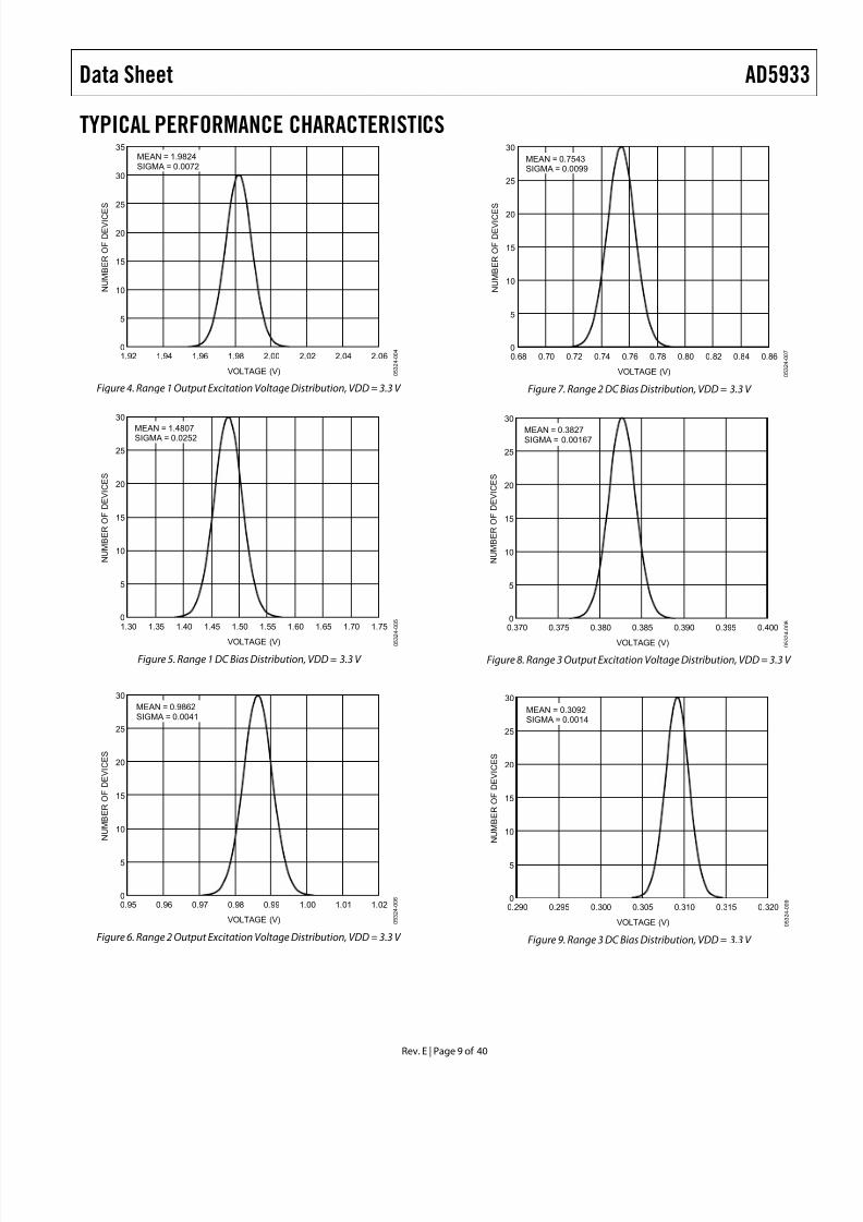
TYPICAL PERFORMANCE CHARACTERISTICS35
0
N U M B E R
O F D E V I C E
S
30
25
20
15
10
5
2.06
VOLTAGE (V)
1.92 1.94 1.96 1.98 2.00 2.02 2.04
MEAN = 1.9824SIGMA = 0.0072
0 5 3 2 4 - 0 0 4
Figure 4. Range 1 Output Excitation Voltage Distribution, VDD = 3.3 V
1.30 1.75
VOLTAGE (V)
1.35 1.40 1.45 1.50 1.55 1.60 1.65 1.70
MEAN = 1.4807SIGMA = 0.0252
0
N U M B E R
O F D E V I C E S
30
25
20
15
10
5
0 5
3 2 4 - 0 0 5
Figure 5. Range 1 DC Bias Distribution, VDD = 3.3 V
30
0
N U M B E R
O F D E V I C E S
25
20
15
10
5
VOLTAGE (V)
0.95 0.96 0.97 0.98 0.99 1.00 1.01 1.02
MEAN = 0.9862SIGMA = 0.0041
0 5 3 2 4 - 0 0 6
Figure 6. Range 2 Output Excitation Voltage Distribution, VDD = 3.3 V
0.68 0.86
VOLTAGE (V)
0.70 0.72 0.74 0.76 0.78 0.80 0.82 0.84
MEAN = 0.7543SIGMA = 0.0099
30
0
N U M B E R
O F D E V I C E
S
25
20
15
10
5
0 5 3 2 4 - 0 0 7
Figure 7. Range 2 DC Bias Distribution, VDD = 3.3 V
30
00.370 0.400
VOLTAGE (V)
N U M B E R
O F D E V I C E S
25
20
15
10
5
0.375 0.380 0.385 0.390 0.395
MEAN = 0.3827SIGMA = 0.00167
0 5 3 2 4 - 0 0 8
Figure 8. Range 3 Output Excitation Voltage Distribution, VDD = 3.3 V
0.290 0.320
VOLTAGE (V)
0.295 0.300 0.305 0.310 0.315
MEAN = 0.3092SIGMA = 0.0014
30
0
N U M B E R
O F D E V I C E S
25
20
15
10
5
0 5 3 2 4 - 0 0 9
Figure 9. Range 3 DC Bias Distribution, VDD = 3.3 V
7/22/2019 AD5933 datasheet
http://slidepdf.com/reader/full/ad5933-datasheet 10/40
AD5933 Data Sheet
Rev. E | Page 10 of 40
VOLTAGE (V)
0.192 0.194 0.196 0.198 0.200 0.202 0.204 0.206
MEAN = 0.1982SIGMA = 0.0008
30
0
N U M B E R
O F
D E V I C E S
25
20
15
10
5
0 5 3 2 4 - 0 1 0
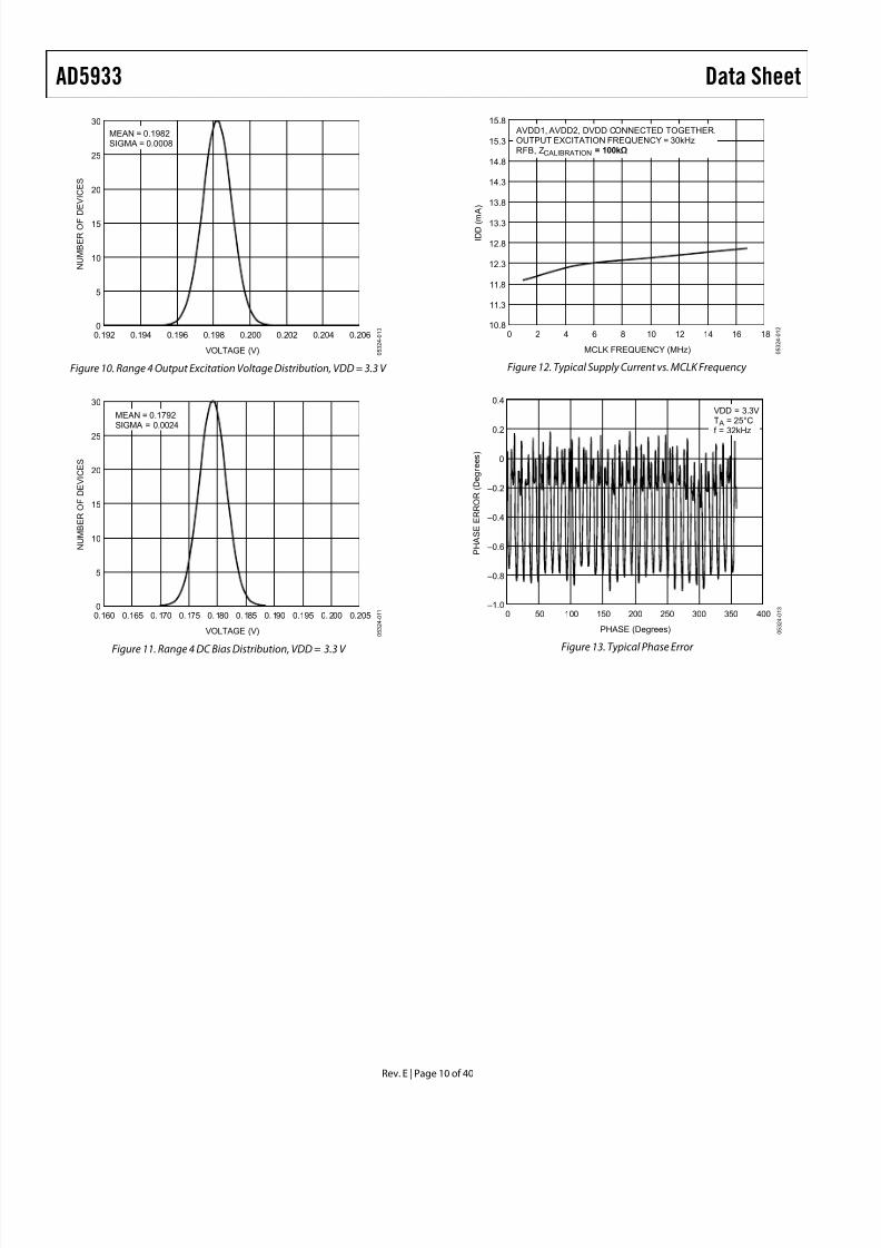
Figure 10. Range 4 Output Excitation Voltage Distribution, VDD = 3.3 V
0.160 0.205
VOLTAGE (V)
0.165 0.170 0.175 0.180 0.185 0.190 0.195 0.200
MEAN = 0.1792SIGMA = 0.0024
30
0
N U M B E R
O F D E V I C E S
25
20
15
10
5
0 5 3 2 4 - 0 1 1
Figure 11. Range 4 DC Bias Distribution, VDD = 3.3 V
15.8
10.80 18
MCLK FREQUENCY (MHz)
I D D ( m
A )
15.3
14.8
14.3
13.8
13.3
12.8
12.3
11.8
11.3
AVDD1, AVDD2, DVDD CONNECTED TOGETHER.OUTPUT EXCITATION FREQUENCY = 30kHzRFB, ZCALIBRATION = 100kΩ
2 4 6 8 10 12 14 16
0 5 3 2 4 - 0 1 2
Figure 12. Typical Supply Current vs. MCLK Frequency
0.4
–1.00 400
PHASE (Degrees)
P H A S E E R R O R
( D e g r e e s )
0.2
0
–0.2
–0.4
–0.6
–0.8
50 100 150 200 250 300 350
VDD = 3.3VT A = 25°Cf = 32kHz
0 5 3 2 4 - 0 1 3
Figure 13. Typical Phase Error

7/22/2019 AD5933 datasheet
http://slidepdf.com/reader/full/ad5933-datasheet 11/40
Data Sheet AD5933
Rev. E | Page 11 of 40
16.4 16.6 16.8 17.0 17.2
OSCILLATOR FREQUENCY (MHz)
C O U
N T
0 5 3 2 4 - 0 1 4
0
2
4
6
8
10
12
N = 106MEAN = 16.8292SD = 0.142904TEMP = –40°C
Figure 14. Frequency Distribution of Internal Oscillator at −40°C
16
0
2
4
6
8
10
12
14
16.4 16.6 16.8 17.0 17.2
OSCILLATOR FREQUENCY (MHz)
C O U N T
0 5 3 2 4 - 0 1 5
N = 100MEAN = 16.7811SD = 0.0881565
TEMP = 25°C
Figure 15. Frequency Distribution of Internal Oscillator at 25°C
16.4 16.6 16.8 17.0 17.2
OSCILLATOR FREQUENCY (MHz)
C O U
N T
0 5 3 2 4 - 0 1 6
0
2
4
6
8
10
12 N = 100MEAN = 16.7257SD = 0.137633TEMP = 125°C
Figure 16. Frequency Distribution of Internal Oscillator at 125°C

7/22/2019 AD5933 datasheet
http://slidepdf.com/reader/full/ad5933-datasheet 12/40
AD5933 Data Sheet
Rev. E | Page 12 of 40
TERMINOLOGYTotal System Accuracy
The AD5933 can accurately measure a range of impedance values to less than 0.5% of the correct impedance value forsupply voltages between 2.7 V to 5.5 V.
Spurious-Free Dynamic Range (SFDR)
Along with the frequency of interest, harmonics of the funda-mental frequency and images of these frequencies are present atthe output of a DDS device. The spurious-free dynamic rangerefers to the largest spur or harmonic present in the band ofinterest. The wideband SFDR gives the magnitude of the largestharmonic or spur relative to the magnitude of the fundamentalfrequency in the 0 Hz to Nyquist bandwidth. The narrow-bandSFDR gives the attenuation of the largest spur or harmonic in abandwidth of ±200 kHz, about the fundamental frequency.
Signal-to-Noise Ratio (SNR)
SNR is the ratio of the rms value of the measured output signalto the rms sum of all other spectral components below theNyquist frequency. The value for SNR is expressed in decibels.
Total Harmonic Distortion (THD)
THD is the ratio of the rms sum of harmonics to the funda-mental, where V1 is the rms amplitude of the fundamentaland V2, V3, V4, V5, and V6 are the rms amplitudes of thesecond through the sixth harmonics. For the AD5933, THDis defined as
V1
V6 V V4V3V2THD
22222 5log20(dB)
+++=

7/22/2019 AD5933 datasheet
http://slidepdf.com/reader/full/ad5933-datasheet 13/40
Data Sheet AD5933
Rev. E | Page 13 of 40
SYSTEM DESCRIPTION
ADC(12 BITS)
VDD/2
DDSCORE
(27 BITS)
DAC
Z(ω)
I2CINTERFACE
IMAGINARYREGISTER
REALREGISTER
MAC CORE(1024 DFT)
LPF
SCL
SDA
MCLK
ROUT VOUT
AD5933
RFB
VIN
PROGRAMMABLEGAIN AMPLIFIER
×5×1
WINDOWINGOF DATA
COS SIN
MICROCONTROLLER
MCLK
0 5 3
2 4 - 0 1 7
TEMPERATURESENSOR
OSCILLATOR
Figure 17. Block Overview
The AD5933 is a high precision impedance converter systemsolution that combines an on-board frequency generator with a12-bit, 1 MSPS ADC. The frequency generator allows an externalcomplex impedance to be excited with a known frequency. Theresponse signal from the impedance is sampled by the on-boardADC and DFT processed by an on-board DSP engine. The DFTalgorithm returns both a real (R) and imaginary (I) data-word ateach frequency point along the sweep. The impedance magnitudeand phase are easily calculated using the following equations:
22
I R Magnitude +=
Phase = tan−1(I /R)
To characterize an impedance profile Z(ω), generally a frequencysweep is required, like that shown in Figure 18.
FREQUENCY
I M P E D A N C E
0 5 3 2 4 - 0 1 8
Figure 18. Impedance vs. Frequency Profile
The AD5933 permits the user to perform a frequency sweep witha user-defined start frequency, frequency resolution, and numberof points in the sweep. In addition, the device allows the user toprogram the peak-to-peak value of the output sinusoidal signal asan excitation to the external unknown impedance connectedbetween the VOUT and VIN pins.
Table 5 gives the four possible output peak-to-peak voltages andthe corresponding dc bias levels for each range for 3.3 V. These
values are ratiometric with VDD. So for a 5 V supply
ppV33.30.598.1 −=×=1Range for VoltageExcitationOutput
ppV24.23.3
0.548.1 −=×=1Range for VoltageBiasDC Output
Table 5. Voltage Levels Respective Bias Levels for 3.3 V
RangeOutput ExcitationVoltage Amplitude Output DC Bias Level
1 1.98 V p-p 1.48 V
2 0.97 V p-p 0.76 V
3 383 mV p-p 0.31 V
4 198 mV p-p 0.173 V
The excitation signal for the transmit stage is provided on-chipusing DDS techniques that permit subhertz resolution. The receivestage receives the input signal current from the unknown impedanceperforms signal processing, and digitizes the result. The clock forthe DDS is generated from either an external reference clock,which is provided by the user at MCLK, or by the internaloscillator. The clock for the DDS is determined by the status ofBit D3 in the control register (see Register Address 0x81 in theRegister Map section).

7/22/2019 AD5933 datasheet
http://slidepdf.com/reader/full/ad5933-datasheet 14/40
AD5933 Data Sheet
Rev. E | Page 14 of 40
TRANSMIT STAGE
As shown in Figure 19, the transmit stage of the AD5933 is madeup of a 27-bit phase accumulator DDS core that provides theoutput excitation signal at a particular frequency. The input tothe phase accumulator is taken from the contents of the start
frequency register (see Register Address 0x82, Register Address0x83, and Register Address 0x84). Although the phase accumu-lator offers 27 bits of resolution, the start frequency register hasthe three most significant bits (MSBs) set to 0 internally; therefore,the user has the ability to program only the lower 24 bits of thestart frequency register.
PHASE ACCUMULATOR
(27 BITS) VOUTDAC
R(GAIN)
VBIAS 0 5 3 2 4 - 0 1 9
Figure 19. Transmit Stage
The AD5933 offers a frequency resolution programmable by the
user down to 0.1 Hz. The frequency resolution is programmed via a 24-bit word loaded serially over the I2C interface to thefrequency increment register.
The frequency sweep is fully described by the programming ofthree parameters: the start frequency, the frequency increment,and the number of increments.
Start Frequency
This is a 24-bit word that is programmed to the on-board RAMat Register Address 0x82, Register Address 0x83, and RegisterAddress 0x84 (see the Register Map section). The required codeloaded to the start frequency register is the result of the formula
shown in Equation 1, based on the master clock frequency and therequired start frequency output from the DDS.
272
4
×
=
MCLK
Frequency Start Output Required
CodeFrequency Start
(1)
For example, if the user requires the sweep to begin at 30 kHz andhas a 16 MHz clock signal connected to MCLK, the code thatneeds to be programmed is given by
0x0F5C282
4
MHz16kHz30 27 ≡×
=CodeFrequency Start
The user programs the value of 0x0F to Register Address 0x82, the value of 0x5C to Register Address 0x83, and the value of 0x28 toRegister Address 0x84.
Frequency Increment
This is a 24-bit word that is programmed to the on-board RAMat Register Address 0x85, Register Address 0x86, and RegisterAddress 0x87 (see the Register Map). The required code loadedto the frequency increment register is the result of the formula
shown in Equation 2, based on the master clock frequency and therequired increment frequency output from the DDS.
272
4
Re×
=
MCLK
Increment Frequency quired
CodeIncrement Frequency
(2)
For example, if the user requires the sweep to have a resolutionof 10 Hz and has a 16 MHz clock signal connected to MCLK, thecode that needs to be programmed is given by
0x00014F
4
MHz16Hz10 ≡
=CodeIncrement Frequency
The user programs the value of 0x00 to Register Address 0x85,the value of 0x01 to Register Address 0x86, and the value of 0x4Fto Register Address 0x87.
Number of Increments
This is a 9-bit word that represents the number of frequencypoints in the sweep. The number is programmed to the on-boardRAM at Register Address 0x88 and Register Address 0x89 (see theRegister Map section). The maximum number of points that can
be programmed is 511.For example, if the sweep needs 150 points, the user programsthe value of 0x00 to Register Address 0x88 and the value of 0x96to Register Address 0x89.
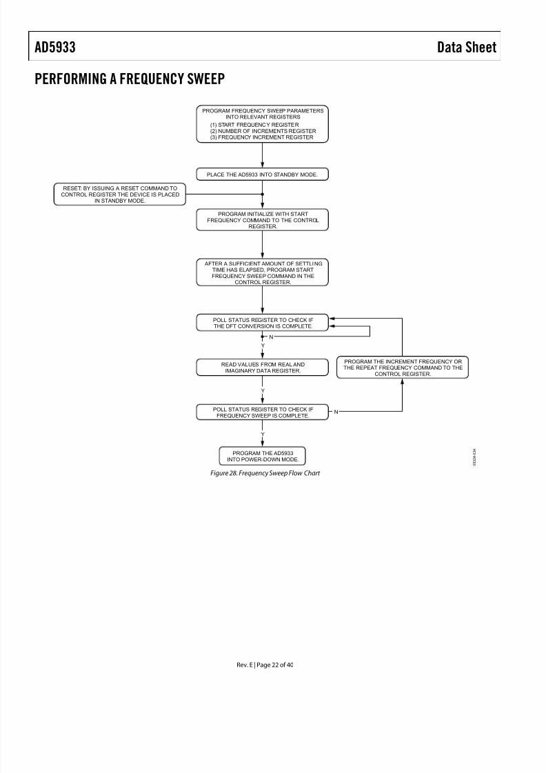
Once the three parameter values have been programmed, thesweep is initiated by issuing a start frequency sweep command tothe control register at Register Address 0x80 and Register Address0x81 (see the Register Map section). Bit D2 in the status register(Register Address 0x8F) indicates the completion of the frequencymeasurement for each sweep point. Incrementing to the nextfrequency sweep point is under the control of the user. Themeasured result is stored in the two register groups that follow:
0x94, 0x95 (real data) and 0x96, 0x97 (imaginary data) that shouldbe read before issuing an increment frequency command to thecontrol register to move to the next sweep point. There is thefacility to repeat the current frequency point measurement byissuing a repeat frequency command to the control register. Thishas the benefit of allowing the user to average successive readings.When the frequency sweep has completed all frequency points,Bit D3 in the status register is set, indicating completion of thesweep. Once this bit is set, further increments are disabled.

7/22/2019 AD5933 datasheet
http://slidepdf.com/reader/full/ad5933-datasheet 15/40
Data Sheet AD5933
Rev. E | Page 15 of 40
FREQUENCY SWEEP COMMAND SEQUENCE
The following sequence must be followed to implement afrequency sweep:
1. Enter standby mode. Prior to issuing a start frequency sweep
command, the device must be placed in a standby mode by
issuing an enter standby mode command to the controlregister (Register Address 0x80 and Register Address 0x81). In this mode, the VOUT and VIN pins are connectedinternally to ground so there is no dc bias across the externalimpedance or between the impedance and ground.
2. Enter initialize mode. In general, high Q complex circuitsrequire a long time to reach steady state. To facilitate themeasurement of such impedances, this mode allows the userfull control of the settling time requirement before enteringstart frequency sweep mode where the impedancemeasurement takes place. An initialize with a start frequency command to the controlregister enters initialize mode. In this mode the impedanceis excited with the programmed start frequency, but no meas-urement takes place. The user times out the required settlingtime before issuing a start frequency sweep command to thecontrol register to enter the start frequency sweep mode.
3. Enter start frequency sweep mode. The user enters this modeby issuing a start frequency sweep command to the controlregister. In this mode, the ADC starts measuring after theprogrammed number of settling time cycles has elapsed. Theuser can program an integer number of output frequencycycles (settling time cycles) to Register Address 0x8A andRegister Address 0x8B before beginning the measurementat each frequency point (see Figure 28).
The DDS output signal is passed through a programmable gainstage to generate the four ranges of peak-to-peak output excitationsignals listed in Table 5. The peak-to-peak output excitation volt-age is selected by setting Bit D10 and Bit D9 in the control register(see the Control Register (Register Address 0X80, RegisterAddress 0X81) section) and is made available at the VOUT pin.
RECEIVE STAGE
The receive stage comprises a current-to-voltage amplifier,followed by a programmable gain amplifier (PGA), antialiasingfilter, and ADC. The receive stage schematic is shown inFigure 20. The unknown impedance is connected between the
VOUT and VIN pins. The first stage current-to-voltage amplifierconfiguration means that a voltage present at the VIN pin is a virtual ground with a dc value set at VDD/2. The signal currentthat is developed across the unknown impedance flows into theVIN pin and develops a voltage signal at the output of the current-to-voltage converter. The gain of the current-to voltage amplifieris determined by a user-selectable feedback resistor connectedbetween Pin 4 (RFB) and Pin 5 (VIN). It is important for the userto choose a feedback resistance value that, in conjunction with theselected gain of the PGA stage, maintains the signal within thelinear range of the ADC (0 V to VDD).
The PGA allows the user to gain the output of the current-to- voltage amplifier by a factor of 5 or 1, depending upon the statusof Bit D8 in the control register (see the Register Map section,Register Address 0x80). The signal is then low-pass filtered andpresented to the input of the 12-bit, 1 MSPS ADC.
5 × R
R
R
R
C
VIN
VDD/2
RFB
ADCLPF
0 5 3 2 4 - 0 2 0
Figure 20. Receive Stage
The digital data from the ADC is passed directly to the DSP coreof the AD5933, which performs a DFT on the sampled data.
DFT OPERATION
A DFT is calculated for each frequency point in the sweep. TheAD5933 DFT algorithm is represented by
∑=
−=1023
0
)))sin())(cos((()(n
n jnnx f X
where: X(f) is the power in the signal at the Frequency Point f.x(n) is the ADC output.cos(n) and sin(n) are the sampled test vectors provided by the
DDS core at the Frequency Point f.The multiplication is accumulated over 1024 samples for eachfrequency point. The result is stored in two, 16-bit registersrepresenting the real and imaginary components of the result.The data is stored in twos complement format.

7/22/2019 AD5933 datasheet
http://slidepdf.com/reader/full/ad5933-datasheet 16/40
AD5933 Data Sheet
Rev. E | Page 16 of 40
SYSTEM CLOCK
The system clock for the AD5933 can be provided in one of twoways. The user can provide a highly accurate and stable systemclock at the external clock pin (MCLK). Alternatively, the AD5933provides an internal clock with a typical frequency of 16.776 MHz
by means of an on-chip oscillator.The user can select the preferred system clock by programmingBit D3 in the control register (Register Address 0x81, seeTable 11). The default clock option on power-up is selected tobe the internal oscillator.
The frequency distribution of the internal clock with temperaturecan be seen in Figure 14, Figure 15, and Figure 16.
TEMPERATURE SENSOR
The temperature sensor is a 13-bit digital temperature sensor witha 14th bit that acts as a sign bit. The on-chip temperature sensorallows an accurate measurement of the ambient device temper-
ature to be made.The measurement range of the sensor is −40°C to +125°C. At+150°C, the structural integrity of the device starts to deterioratewhen operated at voltage and temperature maximum specifica-tions. The accuracy within the measurement range is ±2°C.
TEMPERATURE CONVERSION DETAILS
The conversion clock for the part is internally generated; noexternal clock is required except when reading from and writingto the serial port. In normal mode, an internal clock oscillatorruns an automatic conversion sequence.
The temperature sensor block defaults to a power-down state.To perform a measurement, a measure temperature commandis issued by the user to the control register (Register Address 0x80and Register Address 0x81). After the temperature operation iscomplete (typically 800 μs later), the block automaticallypowers down until the next temperature command is issued.
The user can poll the status register (Register Address 0x8F) to seeif a valid temperature conversion has taken place, indicating that
valid temperature data is available to read at Register Address0x92 and Register Address 0x93 (see the Register Map section).
TEMPERATURE VALUE REGISTER
The temperature value register is a 16-bit, read-only register thatstores the temperature reading from the ADC in 14-bit, twos
complement format. The two MSB bits are don’t cares. D13 is thesign bit. The internal temperature sensor is guaranteed to a low
value limit of –40°C and a high value limit of +150°C. The digitaloutput stored in Register Address 0x92 and Register Address 0x93for the various temperatures is outlined in Table 6. The tempera-ture sensor transfer characteristic is shown in Figure 21.
Table 6. Temperature Data Format
Temperature Digital Output D13…D0
−40°C 11, 1011, 0000, 0000
−30°C 11, 1100, 0100, 0000
−25°C 11, 1100, 1110, 0000
−10°C 11, 1110, 1100, 0000−0.03125°C 11, 1111, 1111, 1111
0°C 00, 0000, 0000, 0000
+0.03125°C 00, 0000, 0000, 0001
+10°C 00, 0001, 0100, 0000
+25°C 00, 0011, 0010, 0000
+50°C 00, 0110, 0100, 0000
+75°C 00, 1001, 0110, 0000
+100°C 00, 1100, 1000, 0000
+125°C 00, 1111, 1010, 0000
+150°C 01, 0010, 1100, 0000
TEMPERATURE CONVERSION FORMULAPositive Temperature = ADC Code (D)/32
Negative Temperature = ( ADC Code (D) – 16384)/32
where ADC Code uses all 14 bits of the data byte, including thesign bit.
Negative Temperature = ( ADC Code (D) – 8192)/32
where ADC Code (D) is D13, the sign bit, and is removed from theADC code.)
D I G I T A L O U T P U
T
–40°C
–0.03125°C
–30°C
11, 1111, 1111, 1111
11, 1100, 0100, 0000
11, 1011, 0000, 0000
TEMPERATURE (°C)
75°C
150°C
01, 0010, 1100, 0000
00, 1001, 0110, 0000
00, 0000, 0000, 0001
0 5 3 2 4 - 0 2 1
Figure 21. Temperature Sensor Transfer Function

7/22/2019 AD5933 datasheet
http://slidepdf.com/reader/full/ad5933-datasheet 17/40
Data Sheet AD5933
Rev. E | Page 17 of 40
IMPEDANCE CALCULATION
MAGNITUDE CALCULATION
The first step in impedance calculation for each frequency pointis to calculate the magnitude of the DFT at that point.
The DFT magnitude is given by22 I R Magnitude +=
where:R is the real number stored at Register Address 0x94 andRegister Address 0x95.I is the imaginary number stored at Register Address 0x96 andRegister Address 0x97.
For example, assume the results in the real data and imaginarydata registers are as follows at a frequency point:
Real data register = 0x038B = 907 decimal
Imaginary data register = 0x0204 = 516 decimal
506.1043)516907( 22 =+= Magnitude
To convert this number into impedance, it must be multipliedbya scaling factor called the gain factor. The gain factor iscalculated during the calibration of the system with a knownimpedance connected between the VOUT and VIN pins.
Once the gain factor has been calculated, it can be used in thecalculation of any unknown impedance between the VOUT andVIN pins.
GAIN FACTOR CALCULATION
An example of a gain factor calculation follows, with thefollowing assumptions:
Output excitation voltage = 2 V p-p
Calibration impedance value, ZCALIBRATION = 200 kΩ
PGA Gain = ×1
Current-to-voltage amplifier gain resistor = 200 kΩ
Calibration frequency = 30 kHz
Then typical contents of the real data and imaginary dataregisters after a frequency point conversion are:
Real data register = 0xF064 = −3996 decimal
Imaginary data register = 0x227E = +8830 decimal
106.9692)8830()3996( 22 =+−= Magnitude
Magnitude
Impedance
Code
AdmittanceFactor Gain
=
=
1
12-10×515.819106.9692
k 200
1
=
Ω
=Factor Gain
IMPEDANCE CALCULATION USING GAIN FACTOR
The next example illustrates how the calculated gain factorderived previously is used to measure an unknown impedance.For this example, assume that the unknown impedance = 510kΩ.
After measuring the unknown impedance at a frequency of30 kHz, assume that the real data and imaginary data registerscontain the following data:
Real data register = 0xFA3F = −1473 decimal
Imaginary data register = 0x0DB3 = +3507 decimal
863.3802))3507()1473(( 22 =+−= Magnitude
Then the measured impedance at the frequency point is givenby
Impedance MagnitudeFactor Gain ×
= 1
=Ω××
=−
k791.509863.380210819273.515
112
GAIN FACTOR VARIATION WITH FREQUENCY
Because the AD5933 has a finite frequency response, the gain
factor also shows a variation with frequency. This variation ingain factor results in an error in the impedance calculation overa frequency range. Figure 22 shows an impedance profile basedon a single-point gain factor calculation. To minimize this error,the frequency sweep should be limited to as small a frequencyrange as possible.
101.5
98.554 66
FREQUENCY (kHz)
I M P E D A N C E ( k Ω )
101.0
100.5
100.0
99.5
99.0
56 58 60 62 64
VDD = 3.3VCALIBRATION FREQUENCY = 60kHzT A = 25°CMEASURED CALIBRATION IMPEDANCE = 100kΩ
0 5 3 2 4 - 0 2 2
Figure 22. Impedance Profile Using a Single-Point Gain Factor Calculation

7/22/2019 AD5933 datasheet
http://slidepdf.com/reader/full/ad5933-datasheet 18/40
AD5933 Data Sheet
Rev. E | Page 18 of 40
TWO-POINT CALIBRATION
Alternatively, it is possible to minimize this error by assumingthat the frequency variation is linear and adjusting the gainfactor with a two-point calibration. Figure 23 shows animpedance profile based on a two-point gain factor calculation.
101.5
98.554 66
FREQUENCY (kHz)
I M P E D A N C E ( k Ω )
101.0
100.5
100.0
99.5
99.0
56 58 60 62 64
VDD = 3.3VCALIBRATION FREQUENCY = 60kHzT A = 25°CMEASURED CALIBRATION IMPEDANCE = 100kΩ
0 5 3 2 4 - 0 2 3
Figure 23. Impedance Profile Using a Two-Point Gain Factor Calculation
TWO-POINT GAIN FACTOR CALCULATION
This is an example of a two-point gain factor calculationassuming the following:
Output excitation voltage = 2 V (p-p)
Calibration impedance value, ZUNKNOWN = 100.0 kΩ
PGA gain = ×1
Supply voltage = 3.3 V
Current-to-voltage amplifier gain resistor = 100 kΩ
Calibration frequencies = 55 kHz and 65 kHzTypical values of the gain factor calculated at the two calibrationfrequencies read
Gain factor calculated at 55 kHz is 1.031224E-09
Gain factor calculated at 65 kHz is 1.035682E-09
Difference in gain factor (∆GF) is 1.035682E-09 −1.031224E-09 = 4.458000E-12
Frequency span of sweep (∆F) = 10 kHz
Therefore, the gain factor required at 60 kHz is given by
9-
10031224.1kHz5kHz10
12-E458000.4
×+
×
The required gain factor is 1.033453E-9.
The impedance is calculated as previously described.
GAIN FACTOR SETUP CONFIGURATION
When calculating the gain factor, it is important that the receivestage operate in its linear region. This requires careful selectionof the excitation signal range, current-to-voltage gain resistor,and PGA gain.
VIN
VDD/2
RFB
ADCLPF
ZUNKNOWNVOUT
CURRENT-TO-VOLTAGEGAIN SETTING RESISTOR
PGA(×1 OR ×5) 0
5 3 2 4 - 0 2 4
Figure 24. System Voltage Gain
The gain through the system shown in Figure 24 is given by
GainPGAZ
sistor Setting Gain
RangeVoltageExcitationOuput
UNKNOWN ×
×
Re
For this example, assume the following system settings:
VDD = 3.3 V
Gain setting resistor = 200 kΩ
ZUNKNOWN = 200 kΩ
PGA setting = ×1
The peak-to-peak voltage presented to the ADC input is2 V p-p. However, if a PGA gain of ×5 was chose, the voltagewould saturate the ADC.
GAIN FACTOR RECALCULATION
The gain factor must be recalculated for a change in any of thefollowing parameters:
• Current-to-voltage gain setting resistor• Output excitation voltage• PGA gain

7/22/2019 AD5933 datasheet
http://slidepdf.com/reader/full/ad5933-datasheet 19/40
Data Sheet AD5933
Rev. E | Page 19 of 40
GAIN FACTOR TEMPERATURE VARIATION
The typical impedance error variation with temperature is inthe order of 30 ppm/°C. Figure 25 shows an impedance profilewith a variation in temperature for 100 kΩ impedance using atwo-point gain factor calibration.
101.5
98.554 66
FREQUENCY (kHz)
I M P E D A N C E ( k Ω )
101.0
100.5
100.0
99.5
99.0
56 58 60 62 64
+125°C
+25°C
VDD = 3.3VCALIBRATION FREQUENCY = 60kHzMEASURED CALIBRATION IMPEDANCE = 100kΩ
0 5 3 2 4 - 0 2 5
–40°C
Figure 25. Impedance Profile Variation with Temperature Using a Two-PointGain Factor Calibration
IMPEDANCE ERROR
It is important when reading the following section to note thatthe output impedance associated with the excitation voltageswas actually measured and then calibrated out for eachimpedance error measurement. This was done using a Keithleycurrent source/sink and measuring the voltage.
R OUT (for example ,200 Ω specified for a 1.98 V p-p in thespecification table) is only a typical specification and can vary
from part to part. This method may not be achievable for large volume applications and in such cases, it is advised to use anextra low impedance output amplifier, as shown in Figure 4, toimprove accuracy.
Please refer to CN-0217 for impedance accuracy examples onthe AD5933 product web-page.
MEASURING THE PHASE ACROSS AN IMPEDANCE
The AD5933 returns a complex output code made up of sepa-rate real and imaginary components. The real component isstored at Register Address 0x94 and Register Address 0x95 andthe imaginary component is stored at Register Address 0x96and Register Address 0x97 after each sweep measurement.
These correspond to the real and imaginary components ofthe DFT and not the resistive and reactive components of theimpedance under test.
For example, it is a very common misconception to assumethat if a user is analyzing a series RC circuit, the real valuestored in Register Address 0x94 and Register Address 0x95and the imaginary value stored at Register Address 0x96and Register Address 0x97 correspond to the resistance andcapacitive reactance, respectfully. However, this is incorrectbecause the magnitude of the impedance (|Z|) can be calculated
by calculating the magnitude of the real and imaginary compo-nents of the DFT given by the following formula:
22 I R Magnitude +=
After each measurement, multiply it by the calibration term and
invert the product. The magnitude of the impedance is, therefore,given by the following formula:
MagnitudeFactor GainImpedance
×=
1
Where gain factor is given by
Magnitude
Impedance
Code
AdmittanceFactor Gain
=
=
1
The user must calibrate the AD5933 system for a knownimpedance range to determine the gain factor before any validmeasurement can take place. Therefore, the user must know theimpedance limits of the complex impedance (ZUNKNOWN) for thesweep frequency range of interest. The gain factor is determinedby placing a known impedance between the input/output of theAD5933 and measuring the resulting magnitude of the code.The AD5933 system gain settings need to be chosen to placethe excitation signal in the linear region of the on-board ADC.
Because the AD5933 returns a complex output code made up ofreal and imaginary components, the user can also calculate thephase of the response signal through the AD5933 signal path.The phase is given by the following formula:
Phase(rads) = tan−1(I /R) (3
The phase measured by Equation 3 accounts for the phase shiftintroduced to the DDS output signal as it passes through theinternal amplifiers on the transmit and receive side of theAD5933 along with the low-pass filter and also the impedanceconnected between the VOUT and VIN pins of the AD5933.
The parameters of interest for many users are the magnitude ofthe impedance (|ZUNKNOWN|) and the impedance phase (ZØ).The measurement of the impedance phase (ZØ) is a two stepprocess.
The first step involves calculating the AD5933 system phase.The AD5933 system phase can be calculated by placing aresistor across the VOUT and VIN pins of the AD5933 and
calculating the phase (using Equation 3) after each measure-ment point in the sweep. By placing a resistor across theVOUT and VIN pins, there is no additional phase lead or lagintroduced to the AD5933 signal path and the resulting phaseis due entirely to the internal poles of the AD5933, that is, thesystem phase.
Once the system phase has been calibrated using a resistor, thesecond step involves calculating the phase of any unknownimpedance by inserting the unknown impedance between theVIN and VOUT terminals of the AD5933 and recalculating the

7/22/2019 AD5933 datasheet
http://slidepdf.com/reader/full/ad5933-datasheet 20/40
AD5933 Data Sheet
Rev. E | Page 20 of 40
new phase (including the phase due to the impedance) usingthe same formula. The phase of the unknown impedance (ZØ)is given by the following formula:
)(Ø systemunknownZ ∇−Φ=
where:system∇ is the phase of the system with a calibration resistor
connected between VIN and VOUT.Φunknown is the phase of the system with the unknownimpedance connected between VIN and VOUT.Z Ø is the phase due to the impedance, that is, the impedancephase.
Note that it is possible to calculate the gain factor and tocalibrate the system phase using the same real and imaginarycomponent values when a resistor is connected between theVOUT and VIN pins of the AD5933, for example, measuringthe impedance phase (ZØ) of a capacitor.
The excitation signal current leads the excitation signal voltageacross a capacitor by −90 degrees. Therefore, an approximate−90 degree phase difference exists between the system phaseresponses measured with a resistor and that of the system phaseresponses measured with a capacitive impedance.
As previously outlined, if the user would like to determine thephase angle of capacitive impedance (ZØ), the user first has todetermine the system phase response ( system∇ ) and subtractthis from the phase calculated with the capacitor connectedbetween VOUT and VIN (Φunknown).
A plot showing the AD5933 system phase response calculatedusing a 220 kΩ calibration resistor (R FB = 220 kΩ, PGA = ×1)
and the repeated phase measurement with a 10 pF capacitiveimpedance is shown in Figure 26.
One important point to note about the phase formula used toplot Figure 26 is that it uses the arctangent function that returnsa phase angle in radians and, therefore, it is necessary to convertfrom radians to degrees.
200
180
160
140
120
100
80
60
40
20
00 15k 30k 45k 60k 75k 90k 105k 120k
FREQUENCY (Hz)
S Y S T E M P H
A S E ( D e g r e e s )
0 5 3 2 4 - 0 3 2
220kΩ RESISTOR
10pF CAPACITOR
Figure 26. System Phase Response vs. Capacitive Phase
The phase difference (that is, ZØ) between the phase responseof a capacitor and the system phase response using a resistor isthe impedance phase of the capacitor, ZØ (see Figure 27).
–100
–90
–80
–70
–60
–50
–40
–30
–20
–10
00 15k 30k 45k 60k 75k 90k 105k 120k
FREQUENCY (Hz)
P H A S E ( D e g r e e s )
0 5 3 2 4 - 0 3 3
Figure 27. Phase Response of a Capacitor
Also when using the real and imaginary values to interpretthe phase at each measurement point, take care when usingthe arctangent formula. The arctangent function returns thecorrect standard phase angle only when the sign of the real andimaginary values are positive, that is, when the coordinates lie
in the first quadrant. The standard angle is the angle takencounterclockwise from the positive real x-axis. If the sign of thereal component is positive and the sign of the imaginarycomponent is negative, that is, the data lies in the secondquadrant, then the arctangent formula returns a negative angleand it is necessary to add a further 180 degrees to calculate thecorrect standard angle. Likewise, when the real and imaginary
components are both negative, that is, when the coordinates liein the third quadrant, then the arctangent formula returns apositive angle and it is necessary to add 180 degrees from theangle to return the correct standard phase. Finally, when thereal component is positive and the imaginary component isnegative, that is, the data lies in the fourth quadrant, then thearctangent formula returns a negative angle. It is necessary toadd 360 degrees to the angle to calculate the correct phaseangle.
Therefore, the correct standard phase angle is dependent uponthe sign of the real and imaginary component and is summa-rized in Table 7.

7/22/2019 AD5933 datasheet
http://slidepdf.com/reader/full/ad5933-datasheet 21/40
Data Sheet AD5933
Rev. E | Page 21 of 40
Once the magnitude of the impedance (|Z|) and the impedancephase angle (ZØ, in radians) are correctly calculated, it is possibleto determine the magnitude of the real (resistive) and imaginary(reactive) component of the impedance (ZUNKNOWN) by the
vector projection of the impedance magnitude onto the realand imaginary impedance axis using the following formulas:
The real component is given by
|Z REAL| = |Z | × cos (Z Ø)
The imaginary component is given by
|Z IMAG| = |Z | × sin (Z Ø)
Table 7. Phase Angle
Real Imaginary Quadrant Phase Angle
Positive Positive First
π×− °180
) /(tan 1
RI
Negative Positive Second( )
×+ −
π
°180/tan°180 1 RI
Negative Negative Third( )
×+ −
π
°180/tan°180 1 RI
Positive Negative Fourth( )
π
×+ − °180/tan°360 1 RI
7/22/2019 AD5933 datasheet
http://slidepdf.com/reader/full/ad5933-datasheet 22/40
AD5933 Data Sheet
Rev. E | Page 22 of 40
PERFORMING A FREQUENCY SWEEP
PROGRAM THE AD5933INTO POWER-DOWN MODE.
PLACE THE AD5933 INTO STANDBY MODE.
PROGRAM FREQUENCY SWEEP PARAMETERSINTO RELEVANT REGISTERS
(1) START FREQUENCY REGISTER (2) NUMBER OF INCREMENTS REGISTER (3) FREQUENCY INCREMENT REGISTER
READ VALUES FROM REAL ANDIMAGINARY DATA REGISTER.
PROGRAM INITIALIZE WITH STARTFREQUENCY COMMAND TO THE CONTROL
REGISTER.
AFTER A SUFFICIENT AMOUNT OF SETTLING
TIME HAS ELAPSED, PROGRAM STARTFREQUENCY SWEEP COMMAND IN THE
CONTROL REGISTER.
POLL STATUS REGISTER TO CHECK IFTHE DFT CONVERSION IS COMPLETE.
RESET: BY ISSUING A RESET COMMAND TOCONTROL REGISTER THE DEVICE IS PLACED
IN STANDBY MODE.
PROGRAM THE INCREMENT FREQUENCY ORTHE REPEAT FREQUENCY COMMAND TO THE
CONTROL REGISTER.
Y
Y
Y
N
NPOLL STATUS REGISTER TO CHECK IF
FREQUENCY SWEEP IS COMPLETE.
0 5 3 2 4 - 0 3 4
Figure 28. Frequency Sweep Flow Chart

7/22/2019 AD5933 datasheet
http://slidepdf.com/reader/full/ad5933-datasheet 23/40
Data Sheet AD5933
Rev. E | Page 23 of 40
REGISTER MAP
Table 8.
Register Name Register Data Function
0x80 Control D15 to D8 Read/write
0x81 D7 to D0 Read/write
0x82 Start frequency D23 to D16 Read/write
0x83 D15 to D8 Read/write
0x84 D7 to D0 Read/write
0x85 Frequency increment D23 to D16 Read/write
0x86 D15 to D8 Read/write
0x87 D7 to D0 Read/write
0x88 Number of increments D15 to D8 Read/write
0x89 D7 to D0 Read/write
0x8A Number of settling time cycles D15 to D8 Read/write
0x8B D7 to D0 Read/write
0x8F Status D7 to D0 Read only
0x92 Temperature data D15 to D8 Read only
0x93 D7 to D0 Read only
0x94 Real data D15 to D8 Read only
0x95 D7 to D0 Read only
0x96 Imaginary data D15 to D8 Read only
0x97 D7 to D0 Read only
CONTROL REGISTER (REGISTER ADDRESS 0x80,REGISTER ADDRESS 0x81)
The AD5933 has a 16-bit control register (Register Address 0x80and Register Address 0x81) that sets the AD5933 controlmodes. The default value of the control register upon reset is
as follows: D15 to D0 reset to 0xA000 upon power-up.The four MSBs of the control register are decoded to providecontrol functions, such as performing a frequency sweep,powering down the part, and controlling various otherfunctions defined in the control register map.
The user may choose to write only to Register Address 0x80 andnot to alter the contents of Register Address 0x81. Note that thecontrol register should not be written to as part of a block writecommand. The control register also allows the user to programthe excitation voltage and set the system clock. A reset commandto the control register does not reset any programmed valuesassociated with the sweep (that is, start frequency, number of
increments, frequency increment). After a reset command, an initialize with start frequency command must be issued to thecontrol register to restart the frequency sweep sequence (seeFigure 28).
Table 9. Control Register Map (D15 to D12)
D15 D14 D13 D12 Function
0 0 0 0 No operation
0 0 0 1 Initialize with start frequency
0 0 1 0 Start frequency sweep
0 0 1 1 Increment frequency0 1 0 0 Repeat frequency
1 0 0 0 No operation
1 0 0 1 Measure temperature
1 0 1 0 Power-down mode
1 0 1 1 Standby mode
1 1 0 0 No operation
1 1 0 1 No operation
Table 10. Control Register Map (D10 to D9)
D10 D9 Range No. Output Voltage Range
0 0 1 2.0 V p-p typical
0 1 4 200 mV p-p typical
1 0 3 400 mV p-p typical1 1 2 1.0 V p-p typical

7/22/2019 AD5933 datasheet
http://slidepdf.com/reader/full/ad5933-datasheet 24/40
AD5933 Data Sheet
Rev. E | Page 24 of 40
Table 11. Control Register Map (D11, D8 to D0)
Bits Description
D11 No operation
D8 PGA gain; 0 = ×5, 1 = ×1
D7 Reserved; set to 0
D6 Reserved; set to 0D5 Reserved; set to 0
D4 Reset
D3 External system clock; set to 1
Internal system clock; set to 0
D2 Reserved; set to 0
D1 Reserved; set to 0
D0 Reserved; set to 0
Control Register Decode
Initialize with Start Frequency
This command enables the DDS to output the programmed
start frequency for an indefinite time. It is used to excite theunknown impedance initially. When the output unknownimpedance has settled after a time determined by the user, theuser must initiate a start frequency sweep command to beginthe frequency sweep.
Start Frequency Sweep
In this mode the ADC starts measuring after the programmednumber of settling time cycles has elapsed. The user has theability to program an integer number of output frequency cycles(settling time cycles) to Register Address 0x8A and RegisterAddress 0x8B before the commencement of the measurementat each frequency point (see Figure 28).
Increment Frequency
The increment frequency command is used to step to the nextfrequency point in the sweep. This usually happens after datafrom the previous step has been transferred and verified by theDSP. When the AD5933 receives this command, it waits for theprogrammed number of settling time cycles before beginningthe ADC conversion process.
Repeat Frequency
The AD5933 has the facility to repeat the current frequencypoint measurement by issuing a repeat frequency command tothe control register. This has the benefit of allowing the user to
average successive readings.Measure Temperature
The measure temperature command initiates a temperaturereading from the part. The part does not need to be in power-up mode to perform a temperature reading. The block powersitself up, takes the reading, and then powers down again. Thetemperature reading is stored in a 14-bit, twos complementformat at Register Address 0x92 and Register Address 0x93.
Power-Down Mode
The default state on power-up of the AD5933 is power-downmode. The control register contains the code 1010,0000,0000,0000(0xA000). In this mode, both the VOUT and VIN pins areconnected internally to GND.
Standby Mode
This mode powers up the part for general operation; in standbymode the VIN and VOUT pins are internally connected to ground.
Output Voltage Range
The output voltage range allows the user to program theexcitation voltage range at VOUT.
PGA Gain
The PGA gain allows the user to amplify the response signalinto the ADC by a multiplication factor of ×5 or ×1.
Reset
A reset command allows the user to interrupt a sweep. The startfrequency, number of increments, and frequency incrementregister contents are not overwritten. An initialize with startfrequency command is required to restart the frequency sweepcommand sequence.
START FREQUENCY REGISTER (REGISTERADDRESS 0x82, REGISTER ADDRESS 0x83,REGISTER ADDRESS 0x84)
The default value of the start frequency register upon reset isas follows: D23 to D0 are not reset on power-up. After a resetcommand, the contents of this register are not reset.
The start frequency register contains the 24-bit digital represen-tation of the frequency from where the subsequent frequencysweep is initiated. For example, if the user requires the sweep tostart from frequency 30 kHz (using a 16.0 MHz clock), then theuser programs the value of 0x0F to Register Address 0x82, the
value of 0x5C to Register Address 0x83, and the value of 0x28 toRegister Address 0x84. This ensures the output frequency startsat 30 kHz.
The code to be programmed to the start frequency register is
28C5F0x02
4
MHz16
kHz3027 ≡×
=CodeFrequency Start

7/22/2019 AD5933 datasheet
http://slidepdf.com/reader/full/ad5933-datasheet 25/40
Data Sheet AD5933
Rev. E | Page 25 of 40
FREQUENCY INCREMENT REGISTER (REGISTERADDRESS 0x85, REGISTER ADDRESS 0x86,REGISTER ADDRESS 0x87)
The default value upon reset is as follows: D23 to D0 are not reseton power-up. After a reset command, the contents of this register
are not reset.The frequency increment register contains a 24-bit represen-tation of the frequency increment between consecutive frequencypoints along the sweep. For example, if the user requires anincrement step of 10 Hz using a 16.0 MHz clock, the usershould program the value of 0x00 to Register Address 0x85, the
value of 0x01 to Register Address 0x86m, and the value of 0x4Fto Register Address 0x87.
The formula for calculating the increment frequency is given by
F00014x02
4MHz16
Hz1027 ≡×
=CodeIncrement Frequency
The user programs the value 0x00 to Register Address 0x85, the value 0x01 to Register Address 0x86, and the value 0x4F toRegister Address 0x87.
NUMBER OF INCREMENTS REGISTER (REGISTERADDRESS 0x88, REGISTER ADDRESS 0x89)
The default value upon reset is as follows: D8 to D0 are not reseton power-up. After a reset command, the contents of thisregister are not reset.
Table 12. Number of Increments Register
Reg Bits Description Function Format
0x88 D15 to D9 Don’t care Read orwrite
Integer numberstored in binaryformatD8 Number of
incrementsRead orwrite
0x89 D8 to D0 Number ofincrements
Read orwrite
Integer numberstored in binaryformat
This register determines the number of frequency points in thefrequency sweep. The number of points is represented by a 9-bitword, D8 to D0. D15 to D9 are don’t care bits. This register, inconjunction with the start frequency register and the incrementfrequency register, determines the frequency sweep range for
the sweep operation. The maximum number of increments thatcan be programmed is 511.
NUMBER OF SETTLING TIME CYCLESREGISTER (REGISTER ADDRESS 0x8A,REGISTER ADDRESS 0x8B)
The default value upon reset is as follows: D10 to D0 are notreset on power-up. After a reset command, the contents of thisregister are not reset (see Table 13).
This register determines the number of output excitation cyclesthat are allowed to pass through the unknown impedance, afterreceipt of a start frequency sweep, increment frequency, or
repeat frequency command, before the ADC is triggered toperform a conversion of the response signal. The number ofsettling time cycles register value determines the delay betweena start frequency sweep/increment frequency /repeat frequencycommand and the time an ADC conversion commences. Thenumber of cycles is represented by a 9-bit word, D8 to D0. The
value programmed into the number of settling time cyclesregister can be increased by a factor of 2 or 4 depending uponthe status of bits D10 to D9. The five most significant bits, D15to D11, are don’t care bits. The maximum number of outputcycles that can be programmed is 511 × 4 = 2044 cycles. Forexample, consider an excitation signal of 30 kHz. Themaximum delay between the programming of this frequency
and the time that this signal is first sampled by the ADC is ≈511 × 4 × 33.33 µs = 68.126 ms. The ADC takes 1024 samples,and the result is stored as real data and imaginary data inRegister Address 0x94 to Register Address 0x97. The conversionprocess takes approximately 1 ms using a 16.777 MHz clock.
Table 13. Number of Settling Times Cycles Register
Register Bits Description Function Format
0x8A D15 to D11 Don’t care Read or write Integer number stored inbinary formatD10 to D9 2-bit decode
D10 D9 Description0 0 Default
0 1 No. of cycles × 2
1 0 Reserved
1 1 No. of cycles × 4
D8 MSB number of settling time cycles
0x8B D7 to D0 Number of settling time cycles Read or write

7/22/2019 AD5933 datasheet
http://slidepdf.com/reader/full/ad5933-datasheet 26/40
AD5933 Data Sheet
Rev. E | Page 26 of 40
STATUS REGISTER (REGISTER ADDRESS 0x8F)
The status register is used to confirm that particular measure-ment tests have been successfully completed. Each of the bitsfrom D7 to D0 indicates the status of a specific functionality ofthe AD5933.
Bit D0 and Bit D4 to Bit D7 are treated as don’t care bits Thesebits do not indicate the status of any measurement.
The status of Bit D1 indicates the status of a frequency pointimpedance measurement. This bit is set when the AD5933 hascompleted the current frequency point impedance measurement.This bit indicates that there is valid real data and imaginary datain Register Address 0x94 to Register Address 0x97. This bit isreset on receipt of a start frequency sweep, increment frequency,repeat frequency, or reset command. This bit is also reset onpower-up.
The status of Bit D2 indicates the status of the programmedfrequency sweep. This bit is set when all programmed incre-
ments to the number of increments register are complete. Thisbit is reset on power-up and on receipt of a reset command.
Table 14. Status Register (Register Address 0x8F)
Control Word Function
0000 0001 Valid temperature measurement
0000 0010 Valid real/imaginary data
0000 0100 Frequency sweep complete
0000 1000 Reserved
0001 0000 Reserved
0010 0000 Reserved
0100 0000 Reserved
1000 0000 Reserved
Valid Temperature Measurement
The valid temperature measurement control word is set when a valid temperature conversion is complete indicating that validtemperature data is available for reading at Register Address0x92 and Register Address 0x93. It is reset when a temperaturemeasurement takes place as a result of a measure temperaturecommand having been issued to the control register (RegisterAddress 0x80 and Register Address 0x81) by the user.
Valid Real/Imaginary Data
D1 is set when data processing for the current frequency pointis finished, indicating real/imaginary data available for reading.D1 is reset when a start frequency sweep/increment frequency/repeat frequency DDS start/increment/repeat command is
issued. D1 is reset to 0 when a reset command is issued to thecontrol register.
Frequency Sweep Complete
D2 is set when data processing for the last frequency point in thesweep is complete. This bit is reset when a start frequency sweepcommand is issued to the control register. This bit is also resetwhen a reset command is issued to the control register.
TEMPERATURE DATA REGISTER(16 BITS—REGISTER ADDRESS 0x92,REGISTER ADDRESS 0x93)
These registers contain a digital representation of the temper-
ature of the AD5933. The values are stored in 16-bit, twoscomplement format. Bit D15 and Bit D14 are don’t care bits.Bit 13 is the sign bit. To convert this number to an actualtemperature, refer to the Temperature Conversion Formulasection.
REAL AND IMAGINARY DATA REGISTERS (16BITS—REGISTER ADDRESS 0x94, REGISTERADDRESS 0x95, REGISTER ADDRESS 0x96,REGISTER ADDRESS 0x97)
The default value upon reset is as follows: these registers are notreset on power-up or on receipt of a reset command. Note thatthe data in these registers is valid only if Bit D1 in the status
register is set, indicating that the processing at the currentfrequency point is complete.
These registers contain a digital representation of the realand imaginary components of the impedance measured forthe current frequency point. The values are stored in 16-bit,twos complement format. To convert this number to an actualimpedance value, the magnitude—√(Real2 + Imaginary 2)—mustbe multiplied by an admittance/code number (called a gainfactor) to give the admittance, and the result inverted to giveimpedance. The gain factor varies for each ac excitation
voltage/gain combination.

7/22/2019 AD5933 datasheet
http://slidepdf.com/reader/full/ad5933-datasheet 27/40
Data Sheet AD5933
Rev. E | Page 27 of 40
SERIAL BUS INTERFACEControl of the AD5933 is carried out via the I2C-compliantserial interface protocol. The AD5933 is connected to this busas a slave device under the control of a master device. TheAD5933 has a 7-bit serial bus slave address. When the device is
powered up, it has a default serial bus address, 0001101 (0x0D).GENERAL I2C TIMING
Figure 29 shows the timing diagram for general read and writeoperations using the I2C-compliant interface.
The master initiates data transfer by establishing a start condition,defined as a high-to-low transition on the serial data line(SDA), while the serial clock line (SCL) remains high. Thisindicates that a data stream follows. The slave responds to thestart condition and shifts in the next 8 bits, consisting of a 7-bitslave address (MSB first) plus an R/W bit that determinesthe direction of the data transfer—that is, whether data iswritten to or read from the slave device (0 = write, 1 = read).
The slave responds by pulling the data line low during the lowperiod before the ninth clock pulse, known as the acknowledgebit, and holding it low during the high period of this clockpulse. All other devices on the bus remain idle while theselected device waits for data to be read from or written to it.If the R/W bit is 0, then the master writes to the slave device.If the R/W bit is 1, the master reads from the slave device.
Data is sent over the serial bus in sequences of nine clockpulses, eight bits of data followed by an acknowledge bit, whichcan be from the master or slave device. Data transitions on thedata line must occur during the low period of the clock signal
and remain stable during the high period, because a low-to-high transition when the clock is high may be interpreted as astop signal. If the operation is a write operation, the first databyte after the slave address is a command byte. This tells theslave device what to expect next. It may be an instruction tellingthe slave device to expect a block write, or it may be a registeraddress that tells the slave where subsequent data is to bewritten. Because data can flow in only one direction as definedby the R/W bit, it is not possible to send a command to a slavedevice during a read operation. Before performing a readoperation, it is sometimes necessary to perform a writeoperation to tell the slave what sort of read operation toexpect and/or the address from which data is to be read.
When all data bytes have been read or written, stop conditionsare established. In write mode, the master pulls the data linehigh during the 10th clock pulse to assert a stop condition. Inread mode, the master device releases the SDA line during thelow period before the ninth clock pulse, but the slave devicedoes not pull it low. This is known as a no acknowledge. Themaster then takes the data line low during the low periodbefore the 10th clock pulse, then high during the 10th clockpulse to assert a stop condition.
0 0 0 1 1 0 1 R/W D7 D6 D5 D4 D3 D2 D1 D0
START CONDITIONBY MASTER
ACKNOWLEDGE BY AD5933
SLAVEADDRESS BYTE ACKNOWLEDGE BYMASTER/SLAVE
SCL
SDA
REGISTER ADDRESS 0 5 3 2 4 - 0 3 5
Figure 29. Timing Diagram

7/22/2019 AD5933 datasheet
http://slidepdf.com/reader/full/ad5933-datasheet 28/40
AD5933 Data Sheet
Rev. E | Page 28 of 40
WRITING/READING TO THE AD5933
The interface specification defines several different protocolsfor different types of read and write operations. This sectiondescribes the protocols used in the AD5933. The figures in thissection use the abbreviations shown in Table 15.
Table 15. I2C Abbreviation Table
Abbreviation Condition
S Start
P Stop
R Read
W Write
A Acknowledge
A No acknowledge write byte/command byte
User Command Codes
The command codes in Table 16 are used for reading/writing tothe interface. They are further explained in this section, but are
grouped here for easy reference.Table 16. Command Codes
CommandCode
CodeName Code Description
1010 0000 Blockwrite
This command is used when writingmultiple bytes to the RAM; see theBlock Write section.
1010 0001 Blockread
This command is used when readingmultiple bytes from RAM/memory;see the Block Read section.
1011 0000 Addresspointer
This command enables the user to setthe address pointer to any location inthe memory. The data contains theaddress of the register to which thepointer should be pointing reworded
Write Byte/Command Byte
In this operation, the master device sends a byte of data to theslave device. The write byte can either be a data byte write to aregister address or can be a command operation. To write datato a register, the command sequence is as follows (see Figure 30):
1. The master device asserts a start condition on SDA.2. The master sends the 7-bit slave address followed by the
write bit (low).3. The addressed slave device asserts an acknowledge on SDA.4. The master sends a register address.5. The slave asserts an acknowledge on SDA.6. The master sends a data byte.7. The slave asserts an acknowledge on SDA.8. The master asserts a stop condition on SDA to end the
transaction.
SSLAVE
ADDRESSREGISTER ADDRESS
REGISTERDATA
AW A A P
0 5 3 2 4 - 0 3 6
Figure 30. Writing Register Data to Register Address
The write byte protocol is also used to set a pointer to anaddress (see Figure 31). This is used for a subsequent single-
byte read from the same address or block read or block writestarting at that address.
To set a register pointer, the following sequence is applied:
1. The master device asserts a start condition on SDA.2. The master sends the 7-bit slave address followed by the
write bit (low).3. The addressed slave device asserts an acknowledge on
SDA.4. The master sends a pointer command code (see Table 16;
a pointer command = 1011 0000).5. The slave asserts an acknowledge on SDA.6. The master sends a data byte (a register address to where
the pointer is to point).7. The slave asserts an acknowledge on SDA.8. The master asserts a stop condition on SDA to end the
transaction.
S AW A A PPOINTER
COMMAND1011 0000
SLAVE ADDRESS
REGISTER ADDRESS
TO POINT TO 0 5 3 2 4 - 0 3 7
Figure 31. Setting Address Pointer to Register Address
BLOCK WRITE
In this operation, the master device writes a block of data to aslave device (see Figure 32). The start address for a block writemust previously have been set. In the case of the AD5933 this isdone by setting a pointer to set the register address.
1. The master device asserts a start condition on SDA.2. The master sends the 7-bit slave address followed by the
write bit (low).3. The addressed slave device asserts an acknowledge on SDA.4. The master sends an 8-bit command code (1010 0000) that
tells the slave device to expect a block write.5. The slave asserts an acknowledge on SDA.6. The master sends a data byte that tells the slave device the
number of data bytes to be sent to it.7. The slave asserts an acknowledge on SDA.8. The master sends the data bytes.9. The slave asserts an acknowledge on SDA after each
data byte.10. The master asserts a stop condition on SDA to end the
transaction.
A A A A AS W A PSLAVE
ADDRESSBLOCKWRITE
NUMBERBYTES WRITE
BYTE 0 BYTE 1 BYTE 2
0 5 3 2 4 - 0 3 8
Figure 32. Writing a Block Write

7/22/2019 AD5933 datasheet
http://slidepdf.com/reader/full/ad5933-datasheet 29/40
Data Sheet AD5933
Rev. E | Page 29 of 40
READ OPERATIONS
The AD5933 uses two I2C read protocols: receive byte andblock read.
Receive Byte
In the AD5933, the receive byte protocol is used to read a singlebyte of data from a register address whose address has previouslybeen set by setting the address pointer.
In this operation, the master device receives a single byte from aslave device as follows (see Figure 33):
1. The master device asserts a start condition on SDA.2. The master sends the 7-bit slave address followed by the
read bit (high).3. The addressed slave device asserts an acknowledge on SDA.4. The master receives a data byte.5. The master asserts a no acknowledge on SDA (the slave
needs to check that master has received data).
6.
The master asserts a stop condition on SDA and thetransaction ends.
S R A A PSLAVE
ADDRESSREGISTER
DATA 0 5 3 2 4 - 0 3 9
Figure 33. Reading Register Data
Block Read
In this operation, the master device reads a block of data from aslave device (see Figure 34). The start address for a block readmust previously have been set by setting the address pointer.
1. The master device asserts a start condition on SDA.
2. The master sends the 7-bit slave address followed by thewrite bit (low).
3. The addressed slave device asserts an acknowledge on SDA.4. The master sends a command code (1010 0001) that tells
the slave device to expect a block read.5. The slave asserts an acknowledge on SDA.6. The master sends a byte-count data byte that tells the slave
how many data bytes to expect.7. The slave asserts an acknowledge on SDA.8. The master asserts a repeat start condition on SDA. This is
required to set the read bit high.9. The master sends the 7-bit slave address followed by the
read bit (high).10. The slave asserts an acknowledge on SDA.11. The master receives the data bytes.12. The master asserts an acknowledge on SDA after each
data byte.13. A no acknowledge is generated after the last byte to signal
the end of the read.14. The master asserts a stop condition on SDA to end the
transaction.
NUMBERBYTES READ
SSLAVE
ADDRESSW A
BLOCKREAD
A A SSLAVE
ADDRESSR A BYTE 0 A BYTE 1 A BYTE 2 A P
0 5 3 2 4 - 0 4 0
Figure 34. Performing a Block Read

7/22/2019 AD5933 datasheet
http://slidepdf.com/reader/full/ad5933-datasheet 30/40
AD5933 Data Sheet
Rev. E | Page 30 of 40
TYPICAL APPLICATIONSMEASURING SMALL IMPEDANCES
The AD5933 is capable of measuring impedance values up to10 MΩ if the system gain settings are chosen correctly for theimpedance subrange of interest.
If the user places a small impedance value (≤500 Ω over thesweep frequency of interest) between the VOUT and VIN pins,it results in an increase in signal current flowing through theimpedance for a fixed excitation voltage in accordance withOhm’s law. The output stage of the transmit side amplifieravailable at the VOUT pin may not be able to provide therequired increase in current through the impedance. To have aunity gain condition about the receive side I-V amplifier, theuser needs to have a similar small value of feedback resistancefor system calibration as outlined in the Gain Factor SetupConfiguration section. The voltage presented at the VIN pin ishard biased at VDD/2 due to the virtual earth on the receive
side I-V amplifier. The increased current sink/sourcerequirement placed on the output of the receive side I-Vamplifier may also cause the amplifier to operate outside ofthe linear region. This causes significant errors in subsequentimpedance measurements.
The value of the output series resistance, R OUT, (see Figure 35) at the VOUT pin must be taken into account when measuringsmall impedances (ZUNKNOWN), specifically when the value ofthe output series resistance is comparable to the value of theimpedance under test (ZUNKNOWN). If the R OUT value is unac-counted for in the system calibration (that is, the gain factorcalculation) when measuring small impedances, there is an
introduced error into any subsequent impedance measurementthat takes place. The introduced error depends on the relativemagnitude of the impedance being tested compared to the valueof the output series resistance.
0 5 3 2 4 - 0 4 8
PGA I-V
VDD/2
RFB
VIN
AD8531 AD820 AD8641 AD8627
VDD
20kΩ
20kΩ 1µF
VDD/2
VOUTROUT
RFB
DDS
2V p-p
R1
R2
ZUNKNOWN
TRANSMIT SIDEOUTPUT AMPLIFIER
Figure 35. Additional External Amplifier Circuit for Measuring SmallImpedances
The value of the output series resistance depends upon theselected output excitation range at VOUT and has a tolerancefrom device to device like all discrete resistors manufactured ina silicon fabrication process. Typical values of the output series
resistance are outlined in Table 17.
Table 17. Output Series Resistance (ROUT) vs. Excitation Range
Parameter Value (Typ) Output Series Resistance Value
Range 1 2 V p-p 200 Ω typ
Range 2 1 V p-p 2.4 kΩ typ
Range 3 0.4 V p-p 1.0 kΩ typ
Range 4 0.2 V p-p 600 Ω typ
Therefore, to accurately calibrate the AD5933 to measure smallimpedances, it is necessary to reduce the signal current byattenuating the excitation voltage sufficiently and also accountfor the R OUT value and factor it into the gain factor calculation
(see the Gain Factor Calculation section).Measuring the R OUT value during device characterization isachieved by selecting the appropriate output excitation range atVOUT and sinking and sourcing a known current at the pin(for example, ±2 mA) and measuring the change in dc voltage.The output series resistance can be calculated by measuring theinverse of the slope (that is, 1/slope) of the resultant I-V plot.
A circuit that helps to minimize the effects of the issuespreviously outlined is shown in Figure 35. The aim of thiscircuit is to place the AD5933 system gain within its linearrange when measuring small impedances by using an additionalexternal amplifier circuit along the signal path. The external
amplifier attenuates the peak-to-peak excitation voltage atVOUT by a suitable choice of resistors (R1 and R2), therebyreducing the signal current flowing through the impedance andminimizing the effect of the output series resistance in theimpedance calculations.
In the circuit shown in Figure 35, ZUNKNOWN recognizes theoutput series resistance of the external amplifier which istypically much less than 1 Ω with feedback applied dependingupon the op amp device used (for example, AD820, AD8641, AD8531) as well as the load current, bandwidth, and gain.
7/22/2019 AD5933 datasheet
http://slidepdf.com/reader/full/ad5933-datasheet 31/40
Data Sheet AD5933
Rev. E | Page 31 of 40
The key point is that the output impedance of the externalamplifier in Figure 35 (which is also in series with ZUNKNOWN)has a far less significant effect on gain factor calibration andsubsequent impedance readings in comparison to connectingthe small impedance directly to the VOUT pin (and directly inseries with R OUT). The external amplifier buffers the unknownimpedance from the effects of R OUT and introduces a smalleroutput impedance in series with ZUNKNOWN.
For example, if the user measures ZUNKNOWN that is known tohave a small impedance value within the range of 90 Ω to110 Ω over the frequency range of 30 kHz to 32 kHz, theuser may not be in a position to measure R OUT directly inthe factory/lab. Therefore, the user may choose to add onan extra amplifier circuit like that shown in Figure 35 to thesignal path of the AD5933. The user must ensure that thechosen external amplifier has a sufficiently low output seriesresistance over the bandwidth of interest in comparison to theimpedance range under test (for an op amp selection guide, see
www.analog.com/opamps). Most amplifiers from AnalogDevices have a curve of closed loop output impedance vs.frequency at different amplifier gains to determine the outputseries impedance at the frequency of interest.
The system settings are
VDD = 3.3 V
VOUT = 2 V p-p
R2 = 20 kΩ
R1 = 4 kΩ
Gain setting resistor = 500 Ω
ZUNKNOWN = 100 ΩPGA setting = ×1
To attenuate the excitation voltage at VOUT, choose a ratioof R1/R2. With the values of R1 = 4 kΩ and R2 = 20 kΩ,attenuate the signal by 1/5th of 2 V p-p = 400 mV. Themaximum current flowing through the impedance is 400 mV/90 Ω = 4.4 mA.
The system is subsequently calibrated using the usual methodwith a midpoint impedance value of 100 Ω, a calibrationresistor, and a feedback resistor at a midfrequency point in thesweep. The dynamic range of the input signal to the receive sideof the AD5933 can be improved by increasing the value of theI-V gain resistor at the RFB pin. For example, increasing the I-Vgain setting resistor at the RFB pin increases the peak-to-peaksignal presented to the ADC input from 400 mV (RFB = 100 Ω)to 2 V p-p (RFB = 500 Ω).
The gain factor calculated is for a 100 Ω resistor connectedbetween VOUT and VIN, assuming the output series resistanceof the external amplifier is small enough to be ignored.
When biasing the circuit shown in Figure 35, note that thereceive side of the AD5933 is hard-biased about VDD/2 bydesign. Therefore, to prevent the output of the externalamplifier (attenuated AD5933 Range 1 excitation signal) fromsaturating the receive side amplifiers of the AD5933, a voltageequal to VDD/2 must be applied to the noninverting terminalof the external amplifier.

7/22/2019 AD5933 datasheet
http://slidepdf.com/reader/full/ad5933-datasheet 32/40
AD5933 Data Sheet
Rev. E | Page 32 of 40
BIOMEDICAL: NONINVASIVE BLOOD IMPEDANCEMEASUREMENT
When a known strain of a virus is added to a blood samplethat already contains a virus, a chemical reaction takes placewhereby the impedance of the blood under certain conditions
changes. By characterizing this effect across different frequencies,it is possible to detect a specific strain of virus. For example, astrain of the disease exhibits a certain characteristic impedanceat one frequency but not at another; therefore, the requirementis to sweep different frequencies to check for different viruses.The AD5933, with its 27-bit phase accumulator, allows forsubhertz frequency tuning.
The AD5933 can be used to inject a stimulus signal throughthe blood sample via a probe. The response signal is analyzed,and the effective impedance of the blood is tabulated. TheAD5933 is ideal for this application because it allows the userto tune to the specific frequency required for each test.
PROBE
2 6
4
ADR43x
AD5933TOP VIEW
(Not to Scale)
10µF0.1µF
7V
ADuC702xTOP VIEW
(Not to Scale)
1 16
2 15
3 14
4 13
5
6 11
7 10
8 9
RFB
12
0 5 3 2 4 - 0 4 1
Figure 36. Measuring a Blood Sample for a Strain of Virus
SENSOR/COMPLEX IMPEDANCE MEASUREMENT
The operational principle of a capacitive proximity sensor isbased on the change of a capacitance in an RLC resonantcircuit. This leads to changes in the resonant frequency of theRLC circuit, which can be evaluated as shown Figure 37.
It is first required to tune the RLC circuit to the area ofresonance. At the resonant frequency, the impedance of theRLC circuit is at a maximum. Therefore, a programmablefrequency sweep and tuning capability is required, which isprovided by the AD5933.
FREQUENCY (Hz)
P R O X I M I
T Y I M P E D A N C E ( Ω )
RESONANTFREQUENCY
CHANGE INRESONANCE DUETO APPROACHING
OBJECT
FO
0 5 3 2 4 - 0 4 2
Figure 37. Detecting a Change in Resonant Frequency
An example of the use of this type of sensor is for a trainproximity measurement system. The magnetic fields of thetrain approaching on the track change the resonant frequencyto an extent that can be characterized. This information can besent back to a mainframe system to show the train location
on the network.Another application for the AD5933 is in parked vehicle detec-tion. The AD5933 is placed in an embedded unit connected toa coil of wire underneath the parking location. The AD5933outputs a single frequency within the 80 kHz to 100 kHzfrequency range, depending upon the wire composition. Thewire can be modeled as a resonant circuit. The coil is calibratedwith a known impedance value and at a known frequency. Theimpedance of the loop is monitored constantly. If a car is parkedover the coil, the impedance of the coil changes and theAD5933 detects the presence of the car.

7/22/2019 AD5933 datasheet
http://slidepdf.com/reader/full/ad5933-datasheet 33/40
Data Sheet AD5933
Rev. E | Page 33 of 40
ELECTRO-IMPEDANCE SPECTROSCOPY
The AD5933 has found use in the area of corrosion monitoring.Corrosion of metals, such as aluminum and steel, can damageindustrial infrastructures and vehicles such as aircraft, ships,and cars. This damage, if left unattended, may lead to premature
failure requiring expensive repairs and/or replacement. Inmany cases, if the onset of corrosion can be detected, it canbe arrested or slowed, negating the requirement for repairs orreplacement. At present, visual inspection is employed to detectcorrosion; however, this is time consuming, expensive, andcannot be employed in hard-to-access areas.
An alternative to visual inspection is automated monitoringusing corrosion sensors. Monitoring is cheaper, less timeconsuming, and can be deployed where visual inspections areimpossible. Electrochemical impedance spectroscopy (EIS) hasbeen used to interrogate corrosion sensors, but at present largelaboratory test instruments are required. The AD5933 offers anaccurate and compact solution for this type of measurement,enabling the development of field deployable sensor systemsthat can measure corrosion rates autonomously.
Mathematically, the corrosion of aluminum is modeled using anRC network that typically consists of a resistance, R S, in serieswith a parallel resistor and capacitor, R P and CP. A system metalwould typically have values as follows: R S is 10 Ω to 10 kΩ,R P 1 is kΩ to 1 MΩ, and CP is 5 µF to 70 µF. Figure 38 showsa typical Bode plot, impedance modulus, and phase angle vs.frequency, for an aluminum corrosion sensor.
100k
100.1
FREQUENCY (Hz)
M O D U
L U S
P H A S E A N G L E
100k
0 5 3 2 4 - 0 4 3
–75
0
–50
–25
1 10 100 1k 10k
100
1k
10k
Figure 38. Bode Plot for Aluminum Corrosion Sensor
To make accurate measurements of these values, the impedanceneeds to be measured over a frequency range of 0.1 Hz to 100 kHz.To ensure that the measurement itself does not introduce a
corrosive effect, the metal needs to be excited with minimal voltage, typically in the ±20 mV range. A nearby processoror control unit such as the ADuC702x would log a singleimpedance sweep from 0.1 kHz to 100 kHz every 10 minutesand download the results back to a control unit. To achievesystem accuracy from the 0.1 kHz to 1 kHz range, the systemclock needs to be scaled down from the 16.776 MHz nominalclock frequency to 500 kHz, typically. The clock scaling can beachieved digitally using an external direct digital synthesizerlike the AD9834 as a programmable divider, which supplies aclock signal to MCLK and which can be controlled digitally bythe nearby microprocessor.

7/22/2019 AD5933 datasheet
http://slidepdf.com/reader/full/ad5933-datasheet 34/40
AD5933 Data Sheet
Rev. E | Page 34 of 40
LAYOUT AND CONFIGURATIONPOWER SUPPLY BYPASSING AND GROUNDING
When accuracy is important in a circuit, carefully consider thepower supply and ground return layout on the board. Theprinted circuit board containing the AD5933 should haveseparate analog and digital sections, each having its own areaof the board. If the AD5933 is in a system where other devicesrequire an AGND-to-DGND connection, the connectionshould be made at one point only. This ground point shouldbe as close as possible to the AD5933.
The power supply to the AD5933 should be bypassed with10 µF and 0.1 µF capacitors. The capacitors should be physicallyas close as possible to the device, with the 0.1 µF capacitorideally right up against the device. The 10 µF capacitors arethe tantalum bead type. It is important that the 0.1 µF capacitorhave low effective series resistance (ESR) and effective seriesinductance (ESI); common ceramic types of capacitors are
suitable. The 0.1 µF capacitor provides a low impedance pathto ground for high frequencies caused by transient currentsdue to internal logic switching.
The power supply line itself should have as large a trace aspossible to provide a low impedance path and reduce glitcheffects on the supply line. Clocks and other fast switchingdigital signals should be shielded from other parts of the board
by digital ground. Avoid crossover of digital and analog signalsif possible. When traces cross on opposite sides of the board,ensure that they run at right angles to each other to reducefeedthrough effects on the board. The best board layouttechnique is the microstrip technique where the componentside of the board is dedicated to the ground plane only, and thesignal traces are placed on the solder side. However, this is notalways possible with a two-layer board.

7/22/2019 AD5933 datasheet
http://slidepdf.com/reader/full/ad5933-datasheet 35/40
Data Sheet AD5933
Rev. E | Page 35 of 40
EVALUATION BOARDThe AD5933 evaluation board allows designers to evaluatethe high performance AD5933 impedance converter withminimum effort.
The evaluation board interfaces to the USB port of a PC. It ispossible to power the entire board from the USB port.
The impedance converter evaluation kit includes a populatedand tested AD5933 printed circuit board. The EVAL-AD5933EBkit is shipped with a CD-ROM that includes self-installingsoftware. Connect the PC to the evaluation board using thesupplied cable.
The software is compatible with Microsoft® Windows® 2000 andWindows XP and Windows 7.
A schematic of the evaluation board is shown in Figure 39 andFigure 40.
USING THE EVALUATION BOARD
The AD5933 evaluation board is a test system designed tosimplify the evaluation of the AD5933. The evaluation boarddata sheet is also available with the evaluation board that givesfull information on operating the evaluation board. Furtherevaluation information is available from www.analog.com.
PROTOTYPING AREA
An area is available on the evaluation board for the user to addadditional circuits to the evaluation test set. Users may want toinclude switches for multiple calibration use.
CRYSTAL OSCILLATOR (XO) vs. EXTERNAL CLOCK
A 16 MHz oscillator is included on the evaluation board.However, this oscillator can be removed and, if required,an external CMOS clock can be connected to the part.
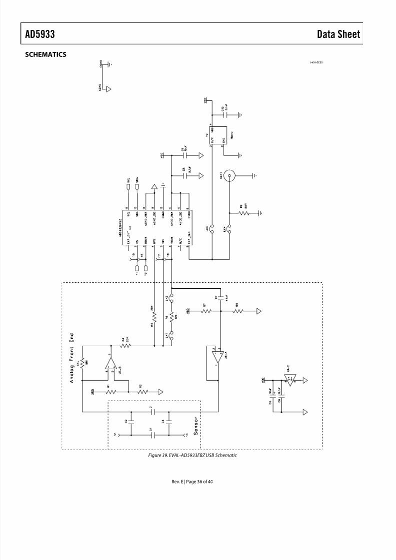
7/22/2019 AD5933 datasheet
http://slidepdf.com/reader/full/ad5933-datasheet 36/40
AD5933 Data Sheet
Rev. E | Page 36 of 40
SCHEMATICS 0 5 3 2 4 - 0 4 4
Figure 39. EVAL-AD5933EBZ USB Schematic

7/22/2019 AD5933 datasheet
http://slidepdf.com/reader/full/ad5933-datasheet 37/40
Data Sheet AD5933
Rev. E | Page 37 of 40
0 5 3 2 4 - 0 4 5
Figure 40. EVAL-AD5933EBZ Schematic

7/22/2019 AD5933 datasheet
http://slidepdf.com/reader/full/ad5933-datasheet 38/40
AD5933 Data Sheet
Rev. E | Page 38 of 40
0 5 3 2 4 - 0 4 6
Figure 41. Linear Regulator on the EVAL-AD5933EB Evaluation Board

7/22/2019 AD5933 datasheet
http://slidepdf.com/reader/full/ad5933-datasheet 39/40
Data Sheet AD5933
Rev. E | Page 39 of 40
0 5 3 2 4 - 0 4 7
Figure 42. Decoupling on the EVAL-AD5933EB Evaluation Board

7/22/2019 AD5933 datasheet
http://slidepdf.com/reader/full/ad5933-datasheet 40/40
AD5933 Data Sheet
OUTLINE DIMENSIONS
COMPLIANT TO JEDEC STANDARDS MO-150-AC 0 6 0 1 0 6 - A
16 9
81
6.50
6.20
5.90
8.20
7.80
7.40
5.60
5.30
5.00
SEATING
PLANE
0.05 MIN
0.65 BSC
2.00 MAX
0.38
0.22COPLANARITY
0.10
1.85
1.75
1.65
0.25
0.09
0.95
0.75
0.55
8°
4°
0°
Figure 43. 16-Lead Shrink Small Outline Package [SSOP](RS-16)
Dimensions shown in millimeters
ORDERING GUIDEModel1, 2 Temperature Range Package Description Package Option
AD5933YRSZ −40°C to +125°C 16-Lead Shrink Small Outline Package (SSOP) RS-16
AD5933YRSZ-REEL7 −40°C to +125°C 16-Lead Shrink Small Outline Package (SSOP) RS-16
AD5933WYRSZ-REEL7 −40°C to +125°C 16-Lead Shrink Small Outline Package (SSOP) RS-16
EVAL-AD5933EBZ −40°C to +125°C Evaluation Board
1 Z = RoHS Compliant Part.2 W = Qualified for Automotive Applications.
AUTOMOTIVE PRODUCTS
The AD5933W models are available with controlled manufacturing to support the quality and reliability requirements of automotive
applications. Note that these automotive models may have specifications that differ from the commercial models; therefore, designersshould review the Specifications section of this data sheet carefully. Only the automotive grade products shown are available for use in
automotive applications. Contact your local Analog Devices account representative for specific product ordering information and to
obtain the specific Automotive Reliability reports for these models.
I2C refers to a communications protocol originally developed by Philips Semiconductors (now NXP Semiconductors).


![Atmel ATmega16U4, ATmega32U4 Datasheet …...ATmega16U4/32U4 [DATASHEET] 8](https://img.dokumen.tips/doc/110x75/5f0a39897e708231d42a9d86/-atmel-atmega16u4-atmega32u4-datasheet-atmega16u432u4-datasheet-8.jpg)
