Embed Size (px)
Citation preview

UA78MXX
INPUT OUTPUT
COMMON0.33 PF 0.1 PF
Unregulated Voltage Source Up to 500 mA
Product
Folder
Sample &Buy
Technical
Documents
Tools &
Software
Support &Community
uA78M05, uA78M06, uA78M08uA78M09, uA78M10, uA78M12, uA78M33
SLVS059T –JUNE 1976–REVISED JANUARY 2015
µA78Mxx Positive-Voltage Regulators1 Features 3 Description
This series of fixed-voltage integrated-circuit voltage1• 3-Terminal Regulators
regulators is designed for a wide range of• Output Current up to 500 mA applications. The applications include on-card• No External Components regulation for elimination of noise and distribution
problems associated with single-point regulation.• Internal Thermal-Overload ProtectionEach of these regulators can deliver up to 500 mA of• High Power-Dissipation Capability output current. The internal current-limiting and
• Internal Short-Circuit Current Limiting thermal-shutdown features of these regulatorsessentially make them immune to overload. In• Output Transistor Safe-Area Compensationaddition to use as fixed-voltage regulators, thesedevices can be used with external components to2 Applicationsobtain adjustable output voltages and currents and
• On-Card Regulation also as the power-pass element in precision• Portable Devices regulators.• Computing & Servers
Device Information(1)• Telecommunications
PART NUMBER PACKAGE BODY SIZE (NOM)SOT-223 (3) 6.50 mm x 3.50 mm
UA78Mxx TO-220 (3) 10.16 mm x 8.82 mmTO-252 (3) 6.60 mm x 6.10 mm
(1) For all available packages, see the orderable addendum atthe end of the data sheet.
4 Simplified Schematic
1
An IMPORTANT NOTICE at the end of this data sheet addresses availability, warranty, changes, use in safety-critical applications,intellectual property matters and other important disclaimers. PRODUCTION DATA.

uA78M05, uA78M06, uA78M08uA78M09, uA78M10, uA78M12, uA78M33SLVS059T –JUNE 1976–REVISED JANUARY 2015 www.ti.com
Table of Contents7.14 Typical Characteristics ............................................ 91 Features .................................................................. 1
8 Detailed Description ............................................ 102 Applications ........................................................... 18.1 Overview ................................................................. 103 Description ............................................................. 18.2 Functional Block Diagram ....................................... 104 Simplified Schematic............................................. 18.3 Feature Description................................................. 105 Revision History..................................................... 28.4 Device Functional Modes........................................ 106 Pin Configuration and Functions ......................... 3
9 Application and Implementation ........................ 117 Specifications......................................................... 49.1 Application Information............................................ 117.1 Absolute Maximum Ratings ...................................... 49.2 Typical Application ................................................. 117.2 ESD Ratings ............................................................ 4
10 Power Supply Recommendations ..................... 137.3 Recommended Operating Conditions....................... 411 Layout................................................................... 137.4 Thermal Information .................................................. 4
11.1 Layout Guidelines ................................................. 137.5 Electrical Characteristics — uA78M33C................... 511.2 Layout Example .................................................... 137.6 Electrical Characteristics — uA78M33I..................... 5
12 Device and Documentation Support ................. 147.7 Electrical Characteristics — uA78M05C................... 612.1 Related Links ........................................................ 147.8 Electrical Characteristics — uA78M05I..................... 612.2 Trademarks ........................................................... 147.9 Electrical Characteristics — uA78M06C................... 712.3 Electrostatic Discharge Caution............................ 147.10 Electrical Characteristics — uA78M08C................. 712.4 Glossary ................................................................ 147.11 Electrical Characteristics — uA78M09C................. 8
13 Mechanical, Packaging, and Orderable7.12 Electrical Characteristics — uA78M10C................. 8Information ........................................................... 147.13 Electrical Characteristics — uA78M12C................. 9
5 Revision History
Changes from Revision S (May 2013) to Revision T Page
• Added Applications, Device Information table, Pin Functions table, ESD Ratings table, Thermal Information table,Typical Characteristics, Feature Description section, Device Functional Modes, Application and Implementationsection, Power Supply Recommendations section, Layout section, Device and Documentation Support section, andMechanical, Packaging, and Orderable Information section. ................................................................................................. 1
Changes from Revision R (February 2013) to Revision S Page
• Removed Ordering Information table. .................................................................................................................................... 1
Changes from Revision Q (April 2010) to Revision R Page
• Removed obsolete part information from document. ............................................................................................................. 1
2 Submit Documentation Feedback Copyright © 1976–2015, Texas Instruments Incorporated
Product Folder Links: uA78M05 uA78M06 uA78M08 uA78M09 uA78M10 uA78M12 uA78M33

DCY (SOT-223) PACKAGE(TOP VIEW)
OUTPUT
COMMON
INPUT
CO
MM
ON
KTP (PowerFLEX /TO-252*) PACKAGE(TOP VIEW)
OUTPUT
COMMON
INPUTCO
MM
ON
* Complies with JEDEC TO-252, variation AC
COMMONOUTPUT
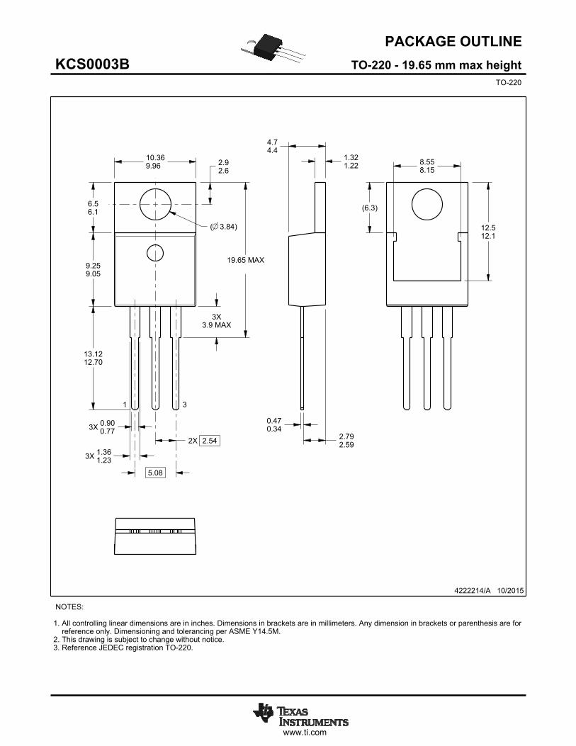
KCS (TO-220) PACKAGE(TOP VIEW)
INPUT
CO
MM
ON
COMMONOUTPUT
KC (TO-220) PACKAGE(TOP VIEW)
INPUT
CO
MM
ON
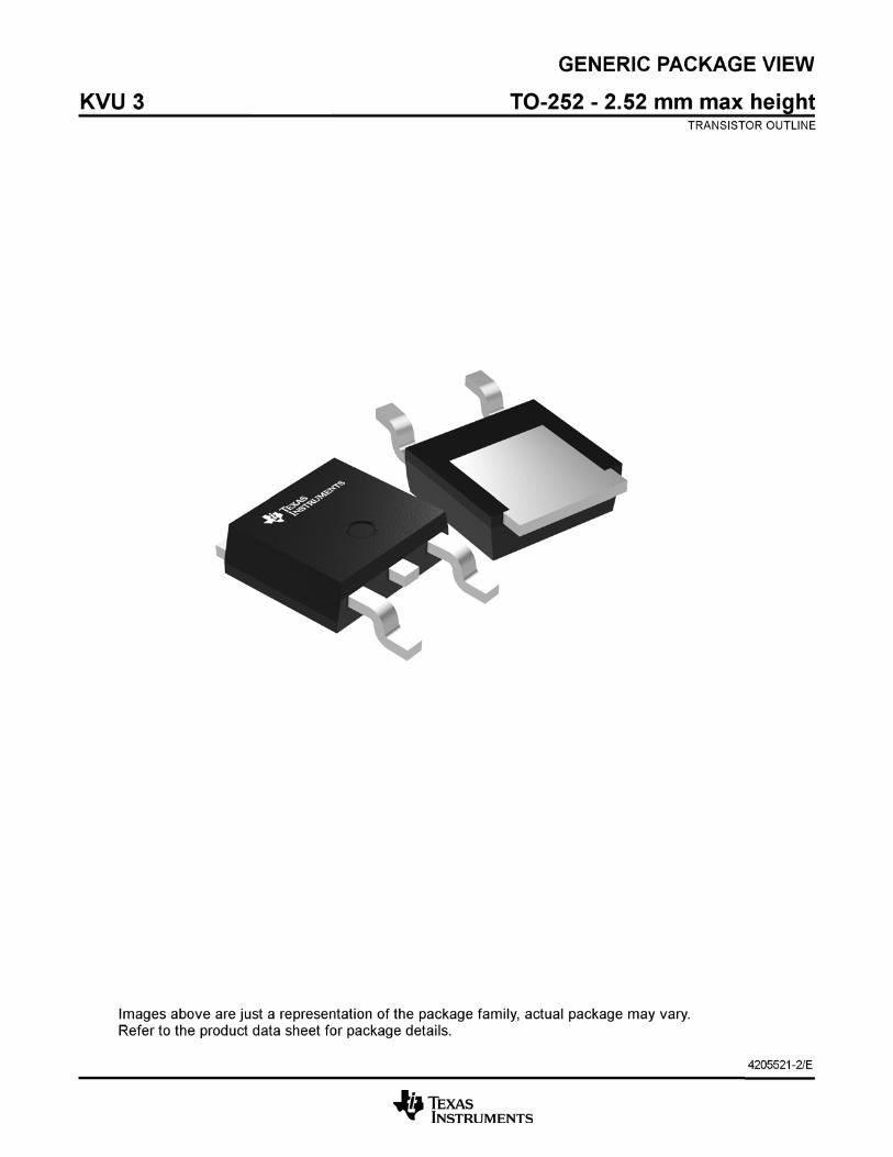
KVU (TO-252) PACKAGE(TOP VIEW)
COMMON
OUTPUT
INPUTCO
MM
ON
uA78M05, uA78M06, uA78M08uA78M09, uA78M10, uA78M12, uA78M33
www.ti.com SLVS059T –JUNE 1976–REVISED JANUARY 2015
6 Pin Configuration and Functions
Pin FunctionsPIN
TYPE DESCRIPTIONNAME NO.COMMON 2 — GroundINPUT 1 I Supply InputOUTPUT 3 O Voltage Output
Copyright © 1976–2015, Texas Instruments Incorporated Submit Documentation Feedback 3
Product Folder Links: uA78M05 uA78M06 uA78M08 uA78M09 uA78M10 uA78M12 uA78M33
uA78M05, uA78M06, uA78M08uA78M09, uA78M10, uA78M12, uA78M33SLVS059T –JUNE 1976–REVISED JANUARY 2015 www.ti.com
7 Specifications
7.1 Absolute Maximum Ratingsover virtual junction temperature range (unless otherwise noted) (1)
MIN MAX UNITVI Input voltage 35 VTJ Operating virtual junction temperature 150 °CTstg Storage temperature range –65 150 °C
(1) Stresses beyond those listed under Absolute Maximum Ratings may cause permanent damage to the device. These are stress ratingsonly, and functional operation of the device at these or any other conditions beyond those indicated under Recommended OperatingConditions is not implied. Exposure to absolute-maximum-rated conditions for extended periods may affect device reliability.
7.2 ESD RatingsVALUE UNIT
Human body model (HBM), per ANSI/ESDA/JEDEC JS-001, all pins (1) 2500V(ESD) Electrostatic discharge VCharged device model (CDM), per JEDEC specification JESD22-C101, 2000all pins (2)
(1) JEDEC document JEP155 states that 500-V HBM allows safe manufacturing with a standard ESD control process.(2) JEDEC document JEP157 states that 250-V CDM allows safe manufacturing with a standard ESD control process.
7.3 Recommended Operating ConditionsMIN MAX UNIT
uA78M33 5.3 25uA78M05 7 25uA78M06 8 25uA78M08 10.5 25
VI Input voltage VuA78M09 11.5 26uA78M10 12.5 28uA78M12 14.5 30uA78M15 17.5 30
IO Output current 500 mAuA78MxxC 0 125
TJ Operating virtual junction temperature °CuA78MxxI –40 125
7.4 Thermal InformationUA78Mxx
THERMAL METRIC (1) DCY KC KCS KTP KVU UNIT3 PINS 3 PINS 3 PINS 3 PINS 3 PINS
RθJA Junction-to-ambient thermal resistance 53 19 19 28 30.3RθJC(to Junction-to-case (top) thermal resistance 30.6 17 17 19 —p) °C/WRθJC(b Junction-to-case (bottom) thermal resistance — 3 3 1.4 —ot)
(1) For more information about traditional and new thermal metrics, see the IC Package Thermal Metrics application report, SPRA953.
4 Submit Documentation Feedback Copyright © 1976–2015, Texas Instruments Incorporated
Product Folder Links: uA78M05 uA78M06 uA78M08 uA78M09 uA78M10 uA78M12 uA78M33
uA78M05, uA78M06, uA78M08uA78M09, uA78M10, uA78M12, uA78M33
www.ti.com SLVS059T –JUNE 1976–REVISED JANUARY 2015
7.5 Electrical Characteristics — uA78M33Cat specified virtual junction temperature, VI = 8 V, IO = 350 mA, TJ = 25°C (unless otherwise noted)
uA78M33CPARAMETER0 TEST CONDITIONS (1) UNIT
MIN TYP MAX3.2 3.3 3.4IO = 5 mA to 350 mA,Output voltage (2) VVI = 8 V to 20 V TJ = 0°C to 125°C 3.1 3.3 3.5
VI = 5.3 V to 25 V 9 100Input voltage regulation IO = 200 mA mV
VI = 8 V to 25 V 3 50IO = 100 mA, TJ = 0°C to 125°C 62VI = 8 V to 18 V,Ripple rejection dBf = 120 Hz IO = 300 mA 62 80
Output voltage regulation VI = 8 V, IO = 5 mA to 500 mA 20 100 mVTemperature coefficient IO = 5 mA, TJ = 0°C to 125°C –1 mV/°Cof output voltageOutput noise voltage f = 10 Hz to 100 kHz 40 200 μVDropout voltage 2 VBias current 4.5 6 mA
IO = 200 mA, VI = 8 V to 25 V, TJ = 0°C to 125°C 0.8Bias current change mA
IO = 5 mA to 350 mA, TJ = 0°C to 125°C 0.5Short-circuit output VI = 35 V 300 mAcurrentPeak output current 700 mA
(1) All characteristics are measured with a 0.33-μF capacitor across the input and a 0.1-μF capacitor across the output. Pulse-testingtechniques maintain TJ as close to TA as possible. Thermal effects must be taken into account separately.
(2) This specification applies only for dc power dissipation permitted by Absolute Maximum Ratings.
7.6 Electrical Characteristics — uA78M33Iat specified virtual junction temperature, VI = 8 V, IO = 350 mA, TJ = 25°C (unless otherwise noted)
uA78M33IPARAMETER TEST CONDITIONS (1) UNIT
MIN TYP MAX3.2 3.3 3.4IO = 5 mA to 350 mA,Output voltage (2) VVI = 8 V to 20 V TJ = –40°C to 125°C 3.1 3.3 3.5
VI = 5.3 V to 25 V 9 100Input voltage regulation IO = 200 mA mV
VI = 8 V to 25 V 3 50IO = 100 mA, TJ = –40°C to 62VI = 8 V to 18 V, 125°CRipple rejection dBf = 120 HzIO = 300 mA 62 80
Output voltage regulation VI = 8 V, IO = 5 mA to 500 mA 20 100 mVTemperature coefficient IO = 5 mA, TJ = –40°C to 125°C –1 mV/°Cof output voltageOutput noise voltage f = 10 Hz to 100 kHz 40 200 μVDropout voltage 2 VBias current 4.5 6 mA
IO = 200 mA, VI = 8 V to 25 V, TJ = –40°C to 125°C 0.8Bias current change mA
IO = 5 mA to 350 mA, TJ = –40°C to 125°C 0.5Short-circuit output VI = 35 V 300 mAcurrentPeak output current 700 mA
(1) All characteristics are measured with a 0.33-μF capacitor across the input and a 0.1-μF capacitor across the output. Pulse-testingtechniques maintain TJ as close to TA as possible. Thermal effects must be taken into account separately.
(2) This specification applies only for dc power dissipation permitted by Absolute Maximum Ratings.
Copyright © 1976–2015, Texas Instruments Incorporated Submit Documentation Feedback 5
Product Folder Links: uA78M05 uA78M06 uA78M08 uA78M09 uA78M10 uA78M12 uA78M33

uA78M05, uA78M06, uA78M08uA78M09, uA78M10, uA78M12, uA78M33SLVS059T –JUNE 1976–REVISED JANUARY 2015 www.ti.com
7.7 Electrical Characteristics — uA78M05Cat specified virtual junction temperature, VI = 10 V, IO = 350 mA, TJ = 25°C (unless otherwise noted)
uA78M05CPARAMETER TEST CONDITIONS (1) UNIT
MIN TYP MAX4.8 5 5.2IO = 5 mA to 350 mA,Output voltage (2) VVI = 7 V to 20 V TJ = 0°C to 125°C 4.75 5.25
VI = 7 V to 25 V 3 100Input voltage regulation IO = 200 mA mV
VI = 8 V to 25 V 1 50IO = 100 mA, TJ = 0°C to 125°C 62VI = 8 V to 18 V,Ripple rejection dBf = 120 Hz IO = 300 mA 62 80
IO = 5 mA to 500 mA 20 100Output voltage regulation mV
IO = 5 mA to 200 mA 10 50Temperature coefficient IO = 5 mA, TJ = 0°C to 125°C –1 mV/°Cof output voltageOutput noise voltage f = 10 Hz to 100 kHz 40 200 μVDropout voltage 2 VBias current 4.5 6 mA
IO = 200 mA, VI = 8 V to 25 V, TJ = 0°C to 125°C 0.8Bias current change mA
IO = 5 mA to 350 mA, TJ = 0°C to 125°C 0.5Short-circuit output current VI = 35 V 300 mAPeak output current 0.7 A
(1) All characteristics are measured with a 0.33-μF capacitor across the input and a 0.1-μF capacitor across the output. Pulse-testingtechniques maintain TJ as close to TA as possible. Thermal effects must be taken into account separately.
(2) This specification applies only for dc power dissipation permitted by Absolute Maximum Ratings.
7.8 Electrical Characteristics — uA78M05Iat specified virtual junction temperature, VI = 10 V, IO = 350 mA, TJ = 25°C (unless otherwise noted)
uA78M05IPARAMETER TEST CONDITIONS (1) UNIT
MIN TYP MAX4.8 5 5.2IO = 5 mA to 350 mA,Output voltage (2) VVI = 7 V to 20 V TJ = –40°C to 125°C 4.75 5.25
VI = 7 V to 25 V 3 100Input voltage regulation IO = 200 mA mV
VI = 8 V to 25 V 1 50IO = 100 mA, TJ = –40°C to 125°C 62VI = 8 V to 18 V,Ripple rejection dBf = 120 Hz IO = 300 mA 62 80
IO = 5 mA to 500 mA 20 100Output voltage mVregulation IO = 5 mA to 200 mA 10 50Temperature coefficient IO = 5 mA, TJ = –40°C to 125°C –1 mV/°Cof output voltageOutput noise voltage f = 10 Hz to 100 kHz 40 200 μVDropout voltage 2 VBias current 4.5 6 mA
IO = 200 mA, VI = 8 V to 25 V, TJ = –40°C to 125°C 0.8Bias current change mA
IO = 5 mA to 350 mA, TJ = –40°C to 125°C 0.5Short-circuit output VI = 35 V 300 mAcurrentPeak output current 0.7 A
(1) All characteristics are measured with a 0.33-μF capacitor across the input and a 0.1-μF capacitor across the output. Pulse-testingtechniques maintain TJ as close to TA as possible. Thermal effects must be taken into account separately.
(2) This specification applies only for dc power dissipation permitted by Absolute Maximum Ratings.
6 Submit Documentation Feedback Copyright © 1976–2015, Texas Instruments Incorporated
Product Folder Links: uA78M05 uA78M06 uA78M08 uA78M09 uA78M10 uA78M12 uA78M33
uA78M05, uA78M06, uA78M08uA78M09, uA78M10, uA78M12, uA78M33
www.ti.com SLVS059T –JUNE 1976–REVISED JANUARY 2015
7.9 Electrical Characteristics — uA78M06Cat specified virtual junction temperature, VI = 11 V, IO = 350 mA, TJ = 25°C (unless otherwise noted)
uA78M06CPARAMETER TEST CONDITIONS (1) UNIT
MIN TYP MAX5.75 6 6.25
Output voltage (2) IO = 5 mA to 350 mA, VI = 8 V to 21 V VTJ = 0°C to 125°C 5.7 6.3
VI = 8 V to 25 V 5 100Input voltage regulation IO = 200 mA mV
VI = 9 V to 25 V 1.5 50IO = 100 mA, 59TJ = 0°C to 125°CRipple rejection VI = 8 V to 18 V, f = 120 Hz dBIO = 300 mA 59 80
IO = 5 mA to 500 mA 20 120Output voltage regulation mV
IO = 5 mA to 200 mA 10 60Temperature coefficient IO = 5 mA, TJ = 0°C to 125°C –1 mV/°Cof output voltageOutput noise voltage f = 10 Hz to 100 kHz 45 μVDropout voltage 2 VBias current 4.5 6 mA
VI = 9 V to 25 V, IO = 200 mA, TJ = 0°C to 125°C 0.8Bias current change mA
IO = 5 mA to 350 mA, TJ = 0°C to 125°C 0.5Short-circuit output current VI = 35 V 270 mAPeak output current 0.7 A
(1) All characteristics are measured with a 0.33-μF capacitor across the input and a 0.1-μF capacitor across the output. Pulse-testingtechniques maintain TJ as close to TA as possible. Thermal effects must be taken into account separately.
(2) This specification applies only for dc power dissipation permitted by Absolute Maximum Ratings.
7.10 Electrical Characteristics — uA78M08Cat specified virtual junction temperature, VI = 14 V, IO = 350 mA, TJ = 25°C (unless otherwise noted)
uA78M08CPARAMETER TEST CONDITIONS (1) UNIT
MIN TYP MAX7.7 8 8.3
Output voltage (2) VI = 10.5 V to 23 V, IO = 5 mA to 350 mA VTJ = 0°C to 125°C 7.6 8.4
VI = 10.5 V to 25 V 6 100Input voltage regulation IO = 200 mA mV
VI = 11 V to 25 V 2 50IO = 100 mA, TJ = 0°C to 125°C 56VI = 11 V to 21.5 V,Ripple rejection dBf = 120 Hz IO = 300 mA 56 80
IO = 5 mA to 500 mA 25 160Output voltage regulation mV
IO = 5 mA to 200 mA 10 80Temperature coefficient IO = 5 mA, TJ = 0°C to 125°C –1 mV/°Cof output voltageOutput noise voltage f = 10 Hz to 100 kHz 52 μVDropout voltage 2 VBias current 4.6 6 mA
VI = 10.5 V to 25 V, IO = 200 mA, TJ = 0°C to 125°C 0.8Bias current change mA
IO = 5 mA to 350 mA, TJ = 0°C to 125°C 0.5Short-circuit output VI = 35 V 250 mAcurrentPeak output current 0.7 A
(1) All characteristics are measured with a 0.33-μF capacitor across the input and a 0.1-μF capacitor across the output. Pulse-testingtechniques maintain TJ as close to TA as possible. Thermal effects must be taken into account separately.
(2) This specification applies only for dc power dissipation permitted by Absolute Maximum Ratings.
Copyright © 1976–2015, Texas Instruments Incorporated Submit Documentation Feedback 7
Product Folder Links: uA78M05 uA78M06 uA78M08 uA78M09 uA78M10 uA78M12 uA78M33

uA78M05, uA78M06, uA78M08uA78M09, uA78M10, uA78M12, uA78M33SLVS059T –JUNE 1976–REVISED JANUARY 2015 www.ti.com
7.11 Electrical Characteristics — uA78M09Cat specified virtual junction temperature, VI = 16 V, IO = 350 mA, TJ = 25°C (unless otherwise noted)
uA78M09CPARAMETER TEST CONDITIONS (1) UNIT
MIN TYP MAX8.6 9 9.4
Output voltage (2) VI = 11.5 V to 24 V, IO = 5 mA to 350 mA VTJ = 0°C to 125°C 8.5 9.5
VI = 11.5 V to 26 V 6 100Input voltage regulation IO = 200 mA mV
VI = 12 V to 26 V 2 50IO = 100 mA, TJ = 0°C to 125°C 56VI = 13 V to 23 V,Ripple rejection dBf = 120 Hz IO = 300 mA 56 80
IO = 5 mA to 500 mA 25 180Output voltage regulation mV
IO = 5 mA to 200 mA 10 90Temperature coefficient IO = 5 mA, TJ = 0°C to 125°C –1 mV/°Cof output voltageOutput noise voltage f = 10 Hz to 100 kHz 58 μVDropout voltage 2 VBias current 4.6 6 mA
VI = 11.5 V to 26 V, IO = 200 mA, TJ = 0°C to 125°C 0.8Bias current change mA
IO = 5 mA to 350 mA, TJ = 0°C to 125°C 0.5Short-circuit output VI = 35 V 250 mAcurrentPeak output current 0.7 A
(1) All characteristics are measured with a 0.33-μF capacitor across the input and a 0.1-μF capacitor across the output. Pulse-testingtechniques maintain TJ as close to TA as possible. Thermal effects must be taken into account separately.
(2) This specification applies only for dc power dissipation permitted by Absolute Maximum Ratings.
7.12 Electrical Characteristics — uA78M10Cat specified virtual junction temperature, VI = 17 V, IO = 350 mA, TJ = 25°C (unless otherwise noted)
uA78M10CPARAMETER TEST CONDITIONS (1) UNIT
MIN TYP MAX9.6 10 10.4
Output voltage (2) VI = 12.5 V to 25 V, IO = 5 mA to 350 mA VTJ = 0°C to 125°C 9.5 10.5
VI = 12.5 V to 28 V 7 100Input voltage regulation IO = 200 mA mV
VI = 14 V to 28 V 2 50IO = 100 mA, TJ = 0°C to 125°C 59VI = 15 V to 25 V,Ripple rejection dBf = 120 Hz IO = 300 mA 55 80
IO = 5 mA to 500 mA 25 200Output voltage regulation mV
IO = 5 mA to 200 mA 10 100Temperature coefficient IO = 5 mA, TJ = 0°C to 125°C –1 mV/°Cof output voltageOutput noise voltage f = 10 Hz to 100 kHz 64 μVDropout voltage 2 VBias current 4.7 6 mA
VI = 12.5 V to 28 V, IO = 200 mA, TJ = 0°C to 125°C 0.8Bias current change mA
IO = 5 mA to 350 mA, TJ = 0°C to 125°C 0.5Short-circuit output VI = 35 V 245 mAcurrentPeak output current 0.7 A
(1) All characteristics are measured with a 0.33-μF capacitor across the input and a 0.1-μF capacitor across the output. Pulse-testingtechniques maintain TJ as close to TA as possible. Thermal effects must be taken into account separately.
(2) This specification applies only for dc power dissipation permitted by Absolute Maximum Ratings.
8 Submit Documentation Feedback Copyright © 1976–2015, Texas Instruments Incorporated
Product Folder Links: uA78M05 uA78M06 uA78M08 uA78M09 uA78M10 uA78M12 uA78M33
0
20
40
60
80
100
120
120Hz 240Hz 500Hz 1KHz
Rip
ple
Reje
ction
(db)
Frequency
Iout at 100 mA
Iout at 300 mA
C002
uA78M05, uA78M06, uA78M08uA78M09, uA78M10, uA78M12, uA78M33
www.ti.com SLVS059T –JUNE 1976–REVISED JANUARY 2015
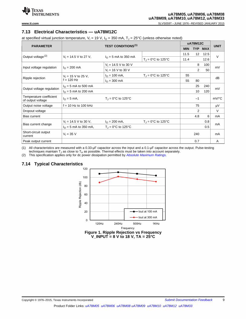
7.13 Electrical Characteristics — uA78M12Cat specified virtual junction temperature, VI = 19 V, IO = 350 mA, TJ = 25°C (unless otherwise noted)
uA78M12CPARAMETER TEST CONDITIONS (1) UNIT
MIN TYP MAX11.5 12 12.5
Output voltage (2) VI = 14.5 V to 27 V, IO = 5 mA to 350 mA VTJ = 0°C to 125°C 11.4 12.6
VI = 14.5 V to 30 V 8 100Input voltage regulation IO = 200 mA mV
VI = 16 V to 30 V 2 50IO = 100 mA, TJ = 0°C to 125°C 55VI = 15 V to 25 V,Ripple rejection dBf = 120 Hz IO = 300 mA 55 80
IO = 5 mA to 500 mA 25 240Output voltage regulation mV
IO = 5 mA to 200 mA 10 120Temperature coefficient IO = 5 mA, TJ = 0°C to 125°C –1 mV/°Cof output voltageOutput noise voltage f = 10 Hz to 100 kHz 75 μVDropout voltage 2 VBias current 4.8 6 mA
VI = 14.5 V to 30 V, IO = 200 mA, TJ = 0°C to 125°C 0.8Bias current change mA
IO = 5 mA to 350 mA, TJ = 0°C to 125°C 0.5Short-circuit output VI = 35 V 240 mAcurrentPeak output current 0.7 A
(1) All characteristics are measured with a 0.33-μF capacitor across the input and a 0.1-μF capacitor across the output. Pulse-testingtechniques maintain TJ as close to TA as possible. Thermal effects must be taken into account separately.
(2) This specification applies only for dc power dissipation permitted by Absolute Maximum Ratings.
7.14 Typical Characteristics
Figure 1. Ripple Rejection vs FrequencyV_INPUT = 8 V to 18 V, TA = 25°C
Copyright © 1976–2015, Texas Instruments Incorporated Submit Documentation Feedback 9
Product Folder Links: uA78M05 uA78M06 uA78M08 uA78M09 uA78M10 uA78M12 uA78M33
140 kΩ
INPUT
96 Ω 0.6 Ω
OUTPUT
0 to 20 kΩ
5.4 kΩ
COMMON
Resistor values shown are nominal.
uA78M05, uA78M06, uA78M08uA78M09, uA78M10, uA78M12, uA78M33SLVS059T –JUNE 1976–REVISED JANUARY 2015 www.ti.com
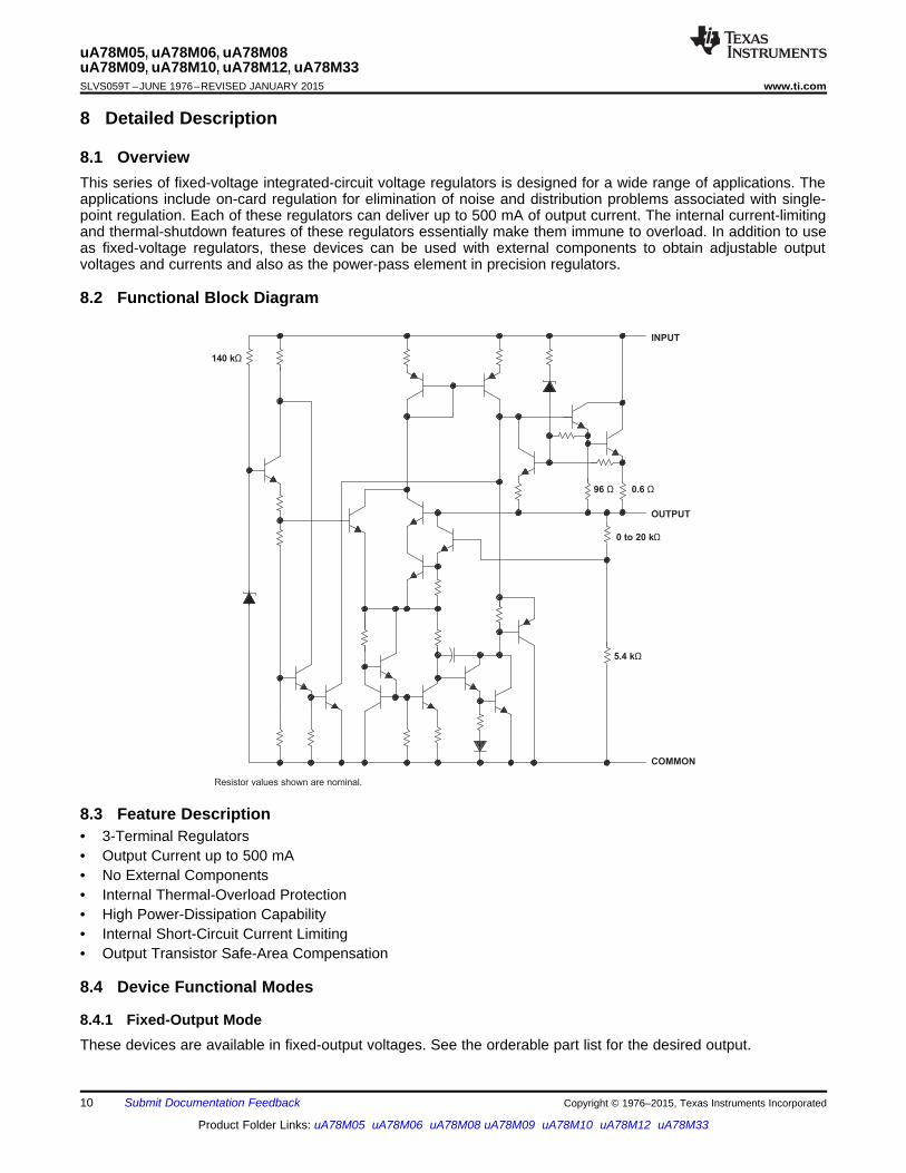
8 Detailed Description
8.1 OverviewThis series of fixed-voltage integrated-circuit voltage regulators is designed for a wide range of applications. Theapplications include on-card regulation for elimination of noise and distribution problems associated with single-point regulation. Each of these regulators can deliver up to 500 mA of output current. The internal current-limitingand thermal-shutdown features of these regulators essentially make them immune to overload. In addition to useas fixed-voltage regulators, these devices can be used with external components to obtain adjustable outputvoltages and currents and also as the power-pass element in precision regulators.
8.2 Functional Block Diagram
8.3 Feature Description• 3-Terminal Regulators• Output Current up to 500 mA• No External Components• Internal Thermal-Overload Protection• High Power-Dissipation Capability• Internal Short-Circuit Current Limiting• Output Transistor Safe-Area Compensation
8.4 Device Functional Modes
8.4.1 Fixed-Output ModeThese devices are available in fixed-output voltages. See the orderable part list for the desired output.
10 Submit Documentation Feedback Copyright © 1976–2015, Texas Instruments Incorporated
Product Folder Links: uA78M05 uA78M06 uA78M08 uA78M09 uA78M10 uA78M12 uA78M33

UA78MXX
INPUT OUTPUT
COMMON0.33 PF 0.1 PF
Unregulated Voltage Source Up to 500 mA
uA78M05, uA78M06, uA78M08uA78M09, uA78M10, uA78M12, uA78M33
www.ti.com SLVS059T –JUNE 1976–REVISED JANUARY 2015
9 Application and Implementation
NOTEInformation in the following applications sections is not part of the TI componentspecification, and TI does not warrant its accuracy or completeness. TI’s customers areresponsible for determining suitability of components for their purposes. Customers shouldvalidate and test their design implementation to confirm system functionality.
9.1 Application InformationThe UA78Mxx devices are ideal for use as linear regulators with few external components needed for a workingdesign. They are also useful for attenuating power supply noise.
9.2 Typical Application
Figure 2. Fixed-Output Regulator
9.2.1 Design RequirementsAn 0.33-µF decoupling capacitor on the input and a 0.1-µF decoupling capacitor on the output are recommendedfor the UA78Mxx to behave as close to datasheet specifications as possible.
9.2.2 Detailed Design ProcedureThe customer's end application will determine how the schematic for UA78Mxx is designed. For example, if thereis a load connected to a negative voltage as its ground, a clamp diode may be necessary on the output. In theevent of an input short circuit or another case where the output voltage can be higher than the input, a diodeshunt can be connected across the device with the anode at the output and cathode at the input
Copyright © 1976–2015, Texas Instruments Incorporated Submit Documentation Feedback 11
Product Folder Links: uA78M05 uA78M06 uA78M08 uA78M09 uA78M10 uA78M12 uA78M33

4.00
4.25
4.50
4.75
5.00
5.25
5.50
6.00 6.25 6.50 6.75 7.00 7.25 7.50 7.75 8.00
Outp
ut
Voltage
(V)
Input Voltage (V)
5 mA
500 mA
C001
uA78M05, uA78M06, uA78M08uA78M09, uA78M10, uA78M12, uA78M33SLVS059T –JUNE 1976–REVISED JANUARY 2015 www.ti.com
Typical Application (continued)9.2.3 Application Curves
Figure 3. V_OUTPUT vs V_INPUT forIOUTPUT = 5 mA and 500 mA (25°C)
12 Submit Documentation Feedback Copyright © 1976–2015, Texas Instruments Incorporated
Product Folder Links: uA78M05 uA78M06 uA78M08 uA78M09 uA78M10 uA78M12 uA78M33
COMMON
OU
TP
UT
CO
MM
ON
INP
UT
PF
Ground
PF
Ground
uA78M05, uA78M06, uA78M08uA78M09, uA78M10, uA78M12, uA78M33
www.ti.com SLVS059T –JUNE 1976–REVISED JANUARY 2015
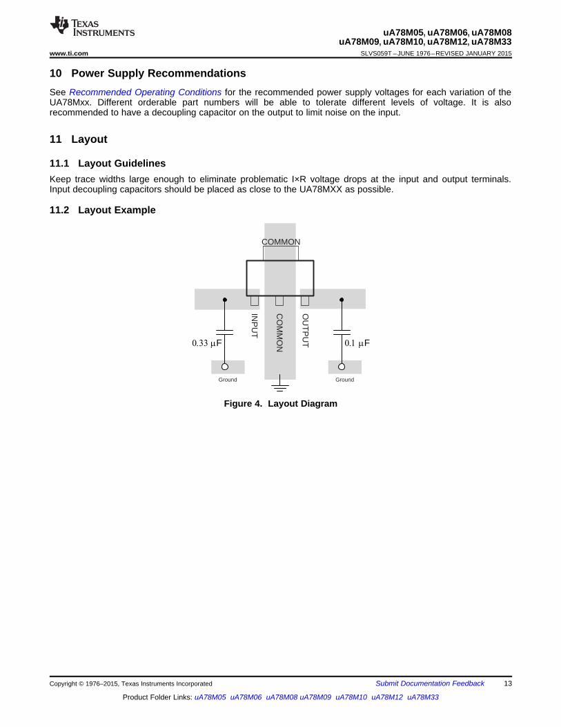
10 Power Supply RecommendationsSee Recommended Operating Conditions for the recommended power supply voltages for each variation of theUA78Mxx. Different orderable part numbers will be able to tolerate different levels of voltage. It is alsorecommended to have a decoupling capacitor on the output to limit noise on the input.
11 Layout
11.1 Layout GuidelinesKeep trace widths large enough to eliminate problematic I×R voltage drops at the input and output terminals.Input decoupling capacitors should be placed as close to the UA78MXX as possible.
11.2 Layout Example
Figure 4. Layout Diagram
Copyright © 1976–2015, Texas Instruments Incorporated Submit Documentation Feedback 13
Product Folder Links: uA78M05 uA78M06 uA78M08 uA78M09 uA78M10 uA78M12 uA78M33
uA78M05, uA78M06, uA78M08uA78M09, uA78M10, uA78M12, uA78M33SLVS059T –JUNE 1976–REVISED JANUARY 2015 www.ti.com
12 Device and Documentation Support
12.1 Related LinksThe table below lists quick access links. Categories include technical documents, support and communityresources, tools and software, and quick access to sample or buy.
Table 1. Related LinksTECHNICAL TOOLS & SUPPORT &PARTS PRODUCT FOLDER SAMPLE & BUY DOCUMENTS SOFTWARE COMMUNITY
uA78M05 Click here Click here Click here Click here Click hereuA78M06 Click here Click here Click here Click here Click hereuA78M08 Click here Click here Click here Click here Click hereuA78M09 Click here Click here Click here Click here Click hereuA78M10 Click here Click here Click here Click here Click hereuA78M12 Click here Click here Click here Click here Click hereuA78M33 Click here Click here Click here Click here Click here
12.2 TrademarksAll trademarks are the property of their respective owners.
12.3 Electrostatic Discharge CautionThese devices have limited built-in ESD protection. The leads should be shorted together or the device placed in conductive foamduring storage or handling to prevent electrostatic damage to the MOS gates.
12.4 GlossarySLYZ022 — TI Glossary.
This glossary lists and explains terms, acronyms, and definitions.
13 Mechanical, Packaging, and Orderable InformationThe following pages include mechanical, packaging, and orderable information. This information is the mostcurrent data available for the designated devices. This data is subject to change without notice and revision ofthis document. For browser-based versions of this data sheet, refer to the left-hand navigation.
14 Submit Documentation Feedback Copyright © 1976–2015, Texas Instruments Incorporated
Product Folder Links: uA78M05 uA78M06 uA78M08 uA78M09 uA78M10 uA78M12 uA78M33
PACKAGE OPTION ADDENDUM
www.ti.com 15-Apr-2017
Addendum-Page 1
PACKAGING INFORMATION
Orderable Device Status(1)
Package Type PackageDrawing
Pins PackageQty
Eco Plan(2)
Lead/Ball Finish(6)
MSL Peak Temp(3)
Op Temp (°C) Device Marking(4/5)
Samples
SN78MCDCYR ACTIVE SOT-223 DCY 4 2500 Green (RoHS& no Sb/Br)
CU SN Level-2-260C-1 YEAR 0 to 125 C5
UA78M05CDCY ACTIVE SOT-223 DCY 4 80 Green (RoHS& no Sb/Br)
CU SN Level-2-260C-1 YEAR 0 to 125 C5
UA78M05CDCYG3 ACTIVE SOT-223 DCY 4 80 Green (RoHS& no Sb/Br)
CU SN Level-2-260C-1 YEAR 0 to 125 C5
UA78M05CDCYR ACTIVE SOT-223 DCY 4 2500 Green (RoHS& no Sb/Br)
CU SN Level-2-260C-1 YEAR 0 to 125 C5
UA78M05CDCYRG3 ACTIVE SOT-223 DCY 4 2500 Green (RoHS& no Sb/Br)
CU SN Level-2-260C-1 YEAR 0 to 125 C5
UA78M05CKCS ACTIVE TO-220 KCS 3 50 Pb-Free(RoHS)
CU SN N / A for Pkg Type 0 to 125 UA78M05C
UA78M05CKCSE3 ACTIVE TO-220 KCS 3 50 Pb-Free(RoHS)
CU SN N / A for Pkg Type 0 to 125 UA78M05C
UA78M05CKVURG3 ACTIVE TO-252 KVU 3 2500 Green (RoHS& no Sb/Br)
CU SN Level-3-260C-168 HR 0 to 125 78M05C
UA78M05IDCY ACTIVE SOT-223 DCY 4 80 Green (RoHS& no Sb/Br)
CU SN Level-2-260C-1 YEAR -40 to 125 J5
UA78M05IDCYG3 ACTIVE SOT-223 DCY 4 80 Green (RoHS& no Sb/Br)
CU SN Level-2-260C-1 YEAR -40 to 125 J5
UA78M05IDCYR ACTIVE SOT-223 DCY 4 2500 Green (RoHS& no Sb/Br)
CU SN Level-2-260C-1 YEAR -40 to 125 J5
UA78M05IDCYRG3 ACTIVE SOT-223 DCY 4 2500 Green (RoHS& no Sb/Br)
CU SN Level-2-260C-1 YEAR -40 to 125 J5
UA78M05IKCS ACTIVE TO-220 KCS 3 50 Pb-Free(RoHS)
CU SN N / A for Pkg Type -40 to 125 UA78M05I
UA78M05IKCSE3 ACTIVE TO-220 KCS 3 50 Pb-Free(RoHS)
CU SN N / A for Pkg Type -40 to 125 UA78M05I
UA78M05IKVURG3 ACTIVE TO-252 KVU 3 2500 Green (RoHS& no Sb/Br)
CU SN Level-3-260C-168 HR -40 to 125 78M05I
UA78M06CKVURG3 ACTIVE TO-252 KVU 3 2500 Green (RoHS& no Sb/Br)
CU SN Level-3-260C-168 HR 0 to 125 78M06C
UA78M08CDCY ACTIVE SOT-223 DCY 4 80 Green (RoHS& no Sb/Br)
CU SN Level-2-260C-1 YEAR 0 to 125 C8

PACKAGE OPTION ADDENDUM
www.ti.com 15-Apr-2017
Addendum-Page 2
Orderable Device Status(1)
Package Type PackageDrawing
Pins PackageQty
Eco Plan(2)
Lead/Ball Finish(6)
MSL Peak Temp(3)
Op Temp (°C) Device Marking(4/5)
Samples
UA78M08CDCYG3 ACTIVE SOT-223 DCY 4 80 Green (RoHS& no Sb/Br)
CU SN Level-2-260C-1 YEAR 0 to 125 C8
UA78M08CDCYR ACTIVE SOT-223 DCY 4 2500 Green (RoHS& no Sb/Br)
CU SN Level-2-260C-1 YEAR 0 to 125 C8
UA78M08CKCS ACTIVE TO-220 KCS 3 50 Pb-Free(RoHS)
CU SN N / A for Pkg Type 0 to 125 UA78M08C
UA78M08CKCSE3 ACTIVE TO-220 KCS 3 50 Pb-Free(RoHS)
CU SN N / A for Pkg Type 0 to 125 UA78M08C
UA78M08CKVURG3 ACTIVE TO-252 KVU 3 2500 Green (RoHS& no Sb/Br)
CU SN Level-3-260C-168 HR 0 to 125 78M08C
UA78M09CKVURG3 ACTIVE TO-252 KVU 3 2500 Green (RoHS& no Sb/Br)
CU SN Level-3-260C-168 HR 0 to 125 78M09C
UA78M10CKVURG3 ACTIVE TO-252 KVU 3 2500 Green (RoHS& no Sb/Br)
CU SN Level-3-260C-168 HR 0 to 125 78M10C
UA78M12CKCS ACTIVE TO-220 KCS 3 50 Pb-Free(RoHS)
CU SN N / A for Pkg Type 0 to 125 UA78M12C
UA78M12CKCSE3 ACTIVE TO-220 KCS 3 50 Pb-Free(RoHS)
CU SN N / A for Pkg Type 0 to 125 UA78M12C
UA78M12CKVURG3 ACTIVE TO-252 KVU 3 2500 Green (RoHS& no Sb/Br)
CU SN Level-3-260C-168 HR 0 to 125 78M12C
UA78M33CDCY ACTIVE SOT-223 DCY 4 80 Green (RoHS& no Sb/Br)
CU SN Level-2-260C-1 YEAR 0 to 125 C3
UA78M33CDCYG3 ACTIVE SOT-223 DCY 4 80 Green (RoHS& no Sb/Br)
CU SN Level-2-260C-1 YEAR 0 to 125 C3
UA78M33CDCYR ACTIVE SOT-223 DCY 4 2500 Green (RoHS& no Sb/Br)
CU SN Level-2-260C-1 YEAR 0 to 125 C3
UA78M33CDCYRG3 ACTIVE SOT-223 DCY 4 2500 Green (RoHS& no Sb/Br)
CU SN Level-2-260C-1 YEAR 0 to 125 C3
UA78M33CKCS ACTIVE TO-220 KCS 3 50 Pb-Free(RoHS)
CU SN N / A for Pkg Type 0 to 125 UA78M33C
UA78M33CKCSE3 ACTIVE TO-220 KCS 3 50 Pb-Free(RoHS)
CU SN N / A for Pkg Type 0 to 125 UA78M33C
UA78M33CKVURG3 ACTIVE TO-252 KVU 3 2500 Green (RoHS& no Sb/Br)
CU SN Level-3-260C-168 HR 0 to 125 78M33C
UA78M33IKVURG3 ACTIVE TO-252 KVU 3 2500 Green (RoHS& no Sb/Br)
CU SN Level-3-260C-168 HR -40 to 125 78M33I
PACKAGE OPTION ADDENDUM
www.ti.com 15-Apr-2017
Addendum-Page 3
(1) The marketing status values are defined as follows:ACTIVE: Product device recommended for new designs.LIFEBUY: TI has announced that the device will be discontinued, and a lifetime-buy period is in effect.NRND: Not recommended for new designs. Device is in production to support existing customers, but TI does not recommend using this part in a new design.PREVIEW: Device has been announced but is not in production. Samples may or may not be available.OBSOLETE: TI has discontinued the production of the device.
(2) Eco Plan - The planned eco-friendly classification: Pb-Free (RoHS), Pb-Free (RoHS Exempt), or Green (RoHS & no Sb/Br) - please check http://www.ti.com/productcontent for the latest availabilityinformation and additional product content details.TBD: The Pb-Free/Green conversion plan has not been defined.Pb-Free (RoHS): TI's terms "Lead-Free" or "Pb-Free" mean semiconductor products that are compatible with the current RoHS requirements for all 6 substances, including the requirement thatlead not exceed 0.1% by weight in homogeneous materials. Where designed to be soldered at high temperatures, TI Pb-Free products are suitable for use in specified lead-free processes.Pb-Free (RoHS Exempt): This component has a RoHS exemption for either 1) lead-based flip-chip solder bumps used between the die and package, or 2) lead-based die adhesive used betweenthe die and leadframe. The component is otherwise considered Pb-Free (RoHS compatible) as defined above.Green (RoHS & no Sb/Br): TI defines "Green" to mean Pb-Free (RoHS compatible), and free of Bromine (Br) and Antimony (Sb) based flame retardants (Br or Sb do not exceed 0.1% by weightin homogeneous material)
(3) MSL, Peak Temp. - The Moisture Sensitivity Level rating according to the JEDEC industry standard classifications, and peak solder temperature.
(4) There may be additional marking, which relates to the logo, the lot trace code information, or the environmental category on the device.
(5) Multiple Device Markings will be inside parentheses. Only one Device Marking contained in parentheses and separated by a "~" will appear on a device. If a line is indented then it is a continuationof the previous line and the two combined represent the entire Device Marking for that device.
(6) Lead/Ball Finish - Orderable Devices may have multiple material finish options. Finish options are separated by a vertical ruled line. Lead/Ball Finish values may wrap to two lines if the finishvalue exceeds the maximum column width.
Important Information and Disclaimer:The information provided on this page represents TI's knowledge and belief as of the date that it is provided. TI bases its knowledge and belief on informationprovided by third parties, and makes no representation or warranty as to the accuracy of such information. Efforts are underway to better integrate information from third parties. TI has taken andcontinues to take reasonable steps to provide representative and accurate information but may not have conducted destructive testing or chemical analysis on incoming materials and chemicals.TI and TI suppliers consider certain information to be proprietary, and thus CAS numbers and other limited information may not be available for release.
In no event shall TI's liability arising out of such information exceed the total purchase price of the TI part(s) at issue in this document sold by TI to Customer on an annual basis.
OTHER QUALIFIED VERSIONS OF UA78M05, UA78M33 :
• Automotive: UA78M05-Q1, UA78M33-Q1

PACKAGE OPTION ADDENDUM
www.ti.com 15-Apr-2017
Addendum-Page 4
NOTE: Qualified Version Definitions:
• Automotive - Q100 devices qualified for high-reliability automotive applications targeting zero defects

TAPE AND REEL INFORMATION
*All dimensions are nominal
Device PackageType
PackageDrawing
Pins SPQ ReelDiameter
(mm)
ReelWidth
W1 (mm)
A0(mm)
B0(mm)
K0(mm)
P1(mm)
W(mm)
Pin1Quadrant
UA78M05CDCYR SOT-223 DCY 4 2500 330.0 12.4 6.55 7.25 1.9 1.5 12.0 Q3
UA78M05CDCYR SOT-223 DCY 4 2500 330.0 12.4 7.0 7.42 2.0 8.0 12.0 Q3
UA78M05CKVURG3 TO-252 KVU 3 2500 330.0 16.4 6.9 10.5 2.7 8.0 16.0 Q2
UA78M05CKVURG3 TO-252 KVU 3 2500 330.0 16.4 6.9 10.5 2.8 8.0 16.0 Q2
UA78M05IDCYR SOT-223 DCY 4 2500 330.0 12.4 7.05 7.4 1.9 8.0 12.0 Q3
UA78M05IDCYR SOT-223 DCY 4 2500 330.0 12.4 7.0 7.42 2.0 8.0 12.0 Q3
UA78M05IDCYR SOT-223 DCY 4 2500 330.0 12.4 6.55 7.25 1.9 1.5 12.0 Q3
UA78M05IKVURG3 TO-252 KVU 3 2500 330.0 16.4 6.9 10.5 2.8 8.0 16.0 Q2
UA78M05IKVURG3 TO-252 KVU 3 2500 330.0 16.4 6.9 10.5 2.7 8.0 16.0 Q2
UA78M06CKVURG3 TO-252 KVU 3 2500 330.0 16.4 6.9 10.5 2.7 8.0 16.0 Q2
UA78M08CDCYR SOT-223 DCY 4 2500 330.0 12.4 7.0 7.42 2.0 8.0 12.0 Q3
UA78M08CDCYR SOT-223 DCY 4 2500 330.0 12.4 7.05 7.4 1.9 8.0 12.0 Q3
UA78M08CKVURG3 TO-252 KVU 3 2500 330.0 16.4 6.9 10.5 2.7 8.0 16.0 Q2
UA78M09CKVURG3 TO-252 KVU 3 2500 330.0 16.4 6.9 10.5 2.7 8.0 16.0 Q2
UA78M10CKVURG3 TO-252 KVU 3 2500 330.0 16.4 6.9 10.5 2.7 8.0 16.0 Q2
UA78M10CKVURG3 TO-252 KVU 3 2500 330.0 16.4 6.9 10.5 2.8 8.0 16.0 Q2
UA78M12CKVURG3 TO-252 KVU 3 2500 330.0 16.4 6.9 10.5 2.7 8.0 16.0 Q2
UA78M33CDCYR SOT-223 DCY 4 2500 330.0 12.4 7.05 7.4 1.9 8.0 12.0 Q3
PACKAGE MATERIALS INFORMATION
www.ti.com 23-May-2017
Pack Materials-Page 1

Device PackageType
PackageDrawing
Pins SPQ ReelDiameter
(mm)
ReelWidth
W1 (mm)
A0(mm)
B0(mm)
K0(mm)
P1(mm)
W(mm)
Pin1Quadrant
UA78M33CDCYR SOT-223 DCY 4 2500 330.0 12.4 7.0 7.42 2.0 8.0 12.0 Q3
UA78M33CDCYR SOT-223 DCY 4 2500 330.0 12.4 6.55 7.25 1.9 1.5 12.0 Q3
UA78M33CKVURG3 TO-252 KVU 3 2500 330.0 16.4 6.9 10.5 2.7 8.0 16.0 Q2
UA78M33IKVURG3 TO-252 KVU 3 2500 330.0 16.4 6.9 10.5 2.8 8.0 16.0 Q2
UA78M33IKVURG3 TO-252 KVU 3 2500 330.0 16.4 6.9 10.5 2.7 8.0 16.0 Q2
*All dimensions are nominal
Device Package Type Package Drawing Pins SPQ Length (mm) Width (mm) Height (mm)
UA78M05CDCYR SOT-223 DCY 4 2500 336.0 336.0 48.0
UA78M05CDCYR SOT-223 DCY 4 2500 350.0 334.0 47.0
UA78M05CKVURG3 TO-252 KVU 3 2500 340.0 340.0 38.0
UA78M05CKVURG3 TO-252 KVU 3 2500 350.0 334.0 47.0
UA78M05IDCYR SOT-223 DCY 4 2500 340.0 340.0 38.0
UA78M05IDCYR SOT-223 DCY 4 2500 350.0 334.0 47.0
UA78M05IDCYR SOT-223 DCY 4 2500 336.0 336.0 48.0
UA78M05IKVURG3 TO-252 KVU 3 2500 350.0 334.0 47.0
UA78M05IKVURG3 TO-252 KVU 3 2500 340.0 340.0 38.0
UA78M06CKVURG3 TO-252 KVU 3 2500 340.0 340.0 38.0
UA78M08CDCYR SOT-223 DCY 4 2500 350.0 334.0 47.0
UA78M08CDCYR SOT-223 DCY 4 2500 340.0 340.0 38.0
PACKAGE MATERIALS INFORMATION
www.ti.com 23-May-2017
Pack Materials-Page 2

Device Package Type Package Drawing Pins SPQ Length (mm) Width (mm) Height (mm)
UA78M08CKVURG3 TO-252 KVU 3 2500 340.0 340.0 38.0
UA78M09CKVURG3 TO-252 KVU 3 2500 340.0 340.0 38.0
UA78M10CKVURG3 TO-252 KVU 3 2500 340.0 340.0 38.0
UA78M10CKVURG3 TO-252 KVU 3 2500 350.0 334.0 47.0
UA78M12CKVURG3 TO-252 KVU 3 2500 340.0 340.0 38.0
UA78M33CDCYR SOT-223 DCY 4 2500 340.0 340.0 38.0
UA78M33CDCYR SOT-223 DCY 4 2500 350.0 334.0 47.0
UA78M33CDCYR SOT-223 DCY 4 2500 336.0 336.0 48.0
UA78M33CKVURG3 TO-252 KVU 3 2500 340.0 340.0 38.0
UA78M33IKVURG3 TO-252 KVU 3 2500 350.0 334.0 47.0
UA78M33IKVURG3 TO-252 KVU 3 2500 340.0 340.0 38.0
PACKAGE MATERIALS INFORMATION
www.ti.com 23-May-2017
Pack Materials-Page 3

www.ti.com
PACKAGE OUTLINE
C
5.4604.953
10.419.40
2.29
4.58
3X 0.8900.635 1.02
0.61
1.270.89
2.52 MAX
0.610.46
4.32MIN
5.21 MIN
-800.130.001.78
1.40
0.610.46
A
6.706.35
B 6.225.97
0.51GAGE PLANE
TO-252 - 2.52 mm max heightKVU0003ATO-252
4218915/A 02/2017
NOTES: 1. All linear dimensions are in millimeters. Any dimensions in parenthesis are for reference only. Dimensioning and tolerancing per ASME Y14.5M. 2. This drawing is subject to change without notice.3. Shape may vary per different assembly sites.4. Reference JEDEC registration TO-252.
1
2
3
0.25 C A BOPTIONAL NOTE 3
SCALE 1.500
SEE DETAIL A
EXPOSEDTHERMAL PAD
NOTE 3
1
2
3
4
A 7.000
DETAIL ATYPICAL

www.ti.com
EXAMPLE BOARD LAYOUT
0.07 MAXALL AROUND 0.07 MIN
ALL AROUND
(6.15)
(5.55)(4.58)
2X (1)2X (2.75)
(4.2) (2.5)(R0.05) TYP
TO-252 - 2.52 mm max heightKVU0003ATO-252
4218915/A 02/2017
LAND PATTERN EXAMPLEEXPOSED METAL SHOWN
SCALE:6X
PKG
SYMM
3
1
4
NOTES: (continued) 5. This package is designed to be soldered to a thermal pad on the board. For more information, see Texas Instruments literature numbers SLMA002(www.ti.com/lit/slm002) and SLMA004 (www.ti.com/lit/slma004).6. Vias are optional depending on application, refer to device data sheet. It is recommended that vias under paste be filled, plugged or tented.
SOLDER MASKOPENING
METAL
EXPOSEDMETAL
SOLDER MASK DETAILSNOT TO SCALE
NON SOLDER MASKDEFINED
METAL UNDERSOLDER MASK
SOLDER MASKOPENING
EXPOSEDMETAL
SOLDER MASKDEFINED

www.ti.com
EXAMPLE STENCIL DESIGN
20X (0.98)20X (1.13)
(R0.05)
2X (2.75)2X (1)
(4.58)
(1.33) TYP
(1.18) TYP
(0.14)
(4.2)
TO-252 - 2.52 mm max heightKVU0003ATO-252
4218915/A 02/2017
PKG
NOTES: (continued) 7. Laser cutting apertures with trapezoidal walls and rounded corners may offer better paste release. IPC-7525 may have alternate design recommendations.8. Board assembly site may have different recommendations for stencil design.
SOLDER PASTE EXAMPLEBASED ON 0.125 mm THICK STENCIL
EXPOSED PAD
65% PRINTED SOLDER COVERAGE BY AREASCALE:8X
SYMM
3
1
4

MECHANICAL DATA
MPDS094A – APRIL 2001 – REVISED JUNE 2002
POST OFFICE BOX 655303 • DALLAS, TEXAS 75265
DCY (R-PDSO-G4) PLASTIC SMALL-OUTLINE
4202506/B 06/2002
6,30 (0.248)6,70 (0.264)
2,90 (0.114)3,10 (0.122)
6,70 (0.264)7,30 (0.287) 3,70 (0.146)
3,30 (0.130)
0,02 (0.0008)0,10 (0.0040)
1,50 (0.059)1,70 (0.067)
0,23 (0.009)0,35 (0.014)
1 2 3
4
0,66 (0.026)0,84 (0.033)
1,80 (0.071) MAX
Seating Plane
0°–10°
Gauge Plane
0,75 (0.030) MIN
0,25 (0.010)
0,08 (0.003)
0,10 (0.004) M
2,30 (0.091)
4,60 (0.181) M0,10 (0.004)
NOTES: A. All linear dimensions are in millimeters (inches).B. This drawing is subject to change without notice.C. Body dimensions do not include mold flash or protrusion.D. Falls within JEDEC TO-261 Variation AA.

www.ti.com
PACKAGE OUTLINE
9.259.05
6.56.1
2.92.6
10.369.96
13.1212.70
3X3.9 MAX
3X 1.361.23
3X 0.900.77
( )3.84
5.08
2X 2.54
8.558.15
12.512.1
(6.3)
19.65 MAX
4.74.4
1.321.22
2.792.59
0.470.34
4222214/A 10/2015
TO-220 - 19.65 mm max heightKCS0003BTO-220
NOTES: 1. All controlling linear dimensions are in inches. Dimensions in brackets are in millimeters. Any dimension in brackets or parenthesis are for reference only. Dimensioning and tolerancing per ASME Y14.5M.2. This drawing is subject to change without notice.3. Reference JEDEC registration TO-220.
1 3
SCALE 0.850

www.ti.com
EXAMPLE BOARD LAYOUT
0.07 MAXALL AROUND
0.07 MAXALL AROUND
(1.7)
3X ( )1.2
(2.54)
(5.08)
R ( )0.05
2X ( )METAL
1.72X SOLDER MASK OPENING
4222214/A 10/2015
TO-220 - 19.65 mm max heightKCS0003BTO-220
LAND PATTERN EXAMPLENON-SOLDER MASK DEFINED
SCALE:15X
1 2 3
OPENINGSOLDER MASK

IMPORTANT NOTICE
Texas Instruments Incorporated (TI) reserves the right to make corrections, enhancements, improvements and other changes to itssemiconductor products and services per JESD46, latest issue, and to discontinue any product or service per JESD48, latest issue. Buyersshould obtain the latest relevant information before placing orders and should verify that such information is current and complete.TI’s published terms of sale for semiconductor products (http://www.ti.com/sc/docs/stdterms.htm) apply to the sale of packaged integratedcircuit products that TI has qualified and released to market. Additional terms may apply to the use or sale of other types of TI products andservices.Reproduction of significant portions of TI information in TI data sheets is permissible only if reproduction is without alteration and isaccompanied by all associated warranties, conditions, limitations, and notices. TI is not responsible or liable for such reproduceddocumentation. Information of third parties may be subject to additional restrictions. Resale of TI products or services with statementsdifferent from or beyond the parameters stated by TI for that product or service voids all express and any implied warranties for theassociated TI product or service and is an unfair and deceptive business practice. TI is not responsible or liable for any such statements.Buyers and others who are developing systems that incorporate TI products (collectively, “Designers”) understand and agree that Designersremain responsible for using their independent analysis, evaluation and judgment in designing their applications and that Designers havefull and exclusive responsibility to assure the safety of Designers' applications and compliance of their applications (and of all TI productsused in or for Designers’ applications) with all applicable regulations, laws and other applicable requirements. Designer represents that, withrespect to their applications, Designer has all the necessary expertise to create and implement safeguards that (1) anticipate dangerousconsequences of failures, (2) monitor failures and their consequences, and (3) lessen the likelihood of failures that might cause harm andtake appropriate actions. Designer agrees that prior to using or distributing any applications that include TI products, Designer willthoroughly test such applications and the functionality of such TI products as used in such applications.TI’s provision of technical, application or other design advice, quality characterization, reliability data or other services or information,including, but not limited to, reference designs and materials relating to evaluation modules, (collectively, “TI Resources”) are intended toassist designers who are developing applications that incorporate TI products; by downloading, accessing or using TI Resources in anyway, Designer (individually or, if Designer is acting on behalf of a company, Designer’s company) agrees to use any particular TI Resourcesolely for this purpose and subject to the terms of this Notice.TI’s provision of TI Resources does not expand or otherwise alter TI’s applicable published warranties or warranty disclaimers for TIproducts, and no additional obligations or liabilities arise from TI providing such TI Resources. TI reserves the right to make corrections,enhancements, improvements and other changes to its TI Resources. TI has not conducted any testing other than that specificallydescribed in the published documentation for a particular TI Resource.Designer is authorized to use, copy and modify any individual TI Resource only in connection with the development of applications thatinclude the TI product(s) identified in such TI Resource. NO OTHER LICENSE, EXPRESS OR IMPLIED, BY ESTOPPEL OR OTHERWISETO ANY OTHER TI INTELLECTUAL PROPERTY RIGHT, AND NO LICENSE TO ANY TECHNOLOGY OR INTELLECTUAL PROPERTYRIGHT OF TI OR ANY THIRD PARTY IS GRANTED HEREIN, including but not limited to any patent right, copyright, mask work right, orother intellectual property right relating to any combination, machine, or process in which TI products or services are used. Informationregarding or referencing third-party products or services does not constitute a license to use such products or services, or a warranty orendorsement thereof. Use of TI Resources may require a license from a third party under the patents or other intellectual property of thethird party, or a license from TI under the patents or other intellectual property of TI.TI RESOURCES ARE PROVIDED “AS IS” AND WITH ALL FAULTS. TI DISCLAIMS ALL OTHER WARRANTIES ORREPRESENTATIONS, EXPRESS OR IMPLIED, REGARDING RESOURCES OR USE THEREOF, INCLUDING BUT NOT LIMITED TOACCURACY OR COMPLETENESS, TITLE, ANY EPIDEMIC FAILURE WARRANTY AND ANY IMPLIED WARRANTIES OFMERCHANTABILITY, FITNESS FOR A PARTICULAR PURPOSE, AND NON-INFRINGEMENT OF ANY THIRD PARTY INTELLECTUALPROPERTY RIGHTS. TI SHALL NOT BE LIABLE FOR AND SHALL NOT DEFEND OR INDEMNIFY DESIGNER AGAINST ANY CLAIM,INCLUDING BUT NOT LIMITED TO ANY INFRINGEMENT CLAIM THAT RELATES TO OR IS BASED ON ANY COMBINATION OFPRODUCTS EVEN IF DESCRIBED IN TI RESOURCES OR OTHERWISE. IN NO EVENT SHALL TI BE LIABLE FOR ANY ACTUAL,DIRECT, SPECIAL, COLLATERAL, INDIRECT, PUNITIVE, INCIDENTAL, CONSEQUENTIAL OR EXEMPLARY DAMAGES INCONNECTION WITH OR ARISING OUT OF TI RESOURCES OR USE THEREOF, AND REGARDLESS OF WHETHER TI HAS BEENADVISED OF THE POSSIBILITY OF SUCH DAMAGES.Unless TI has explicitly designated an individual product as meeting the requirements of a particular industry standard (e.g., ISO/TS 16949and ISO 26262), TI is not responsible for any failure to meet such industry standard requirements.Where TI specifically promotes products as facilitating functional safety or as compliant with industry functional safety standards, suchproducts are intended to help enable customers to design and create their own applications that meet applicable functional safety standardsand requirements. Using products in an application does not by itself establish any safety features in the application. Designers mustensure compliance with safety-related requirements and standards applicable to their applications. Designer may not use any TI products inlife-critical medical equipment unless authorized officers of the parties have executed a special contract specifically governing such use.Life-critical medical equipment is medical equipment where failure of such equipment would cause serious bodily injury or death (e.g., lifesupport, pacemakers, defibrillators, heart pumps, neurostimulators, and implantables). Such equipment includes, without limitation, allmedical devices identified by the U.S. Food and Drug Administration as Class III devices and equivalent classifications outside the U.S.TI may expressly designate certain products as completing a particular qualification (e.g., Q100, Military Grade, or Enhanced Product).Designers agree that it has the necessary expertise to select the product with the appropriate qualification designation for their applicationsand that proper product selection is at Designers’ own risk. Designers are solely responsible for compliance with all legal and regulatoryrequirements in connection with such selection.Designer will fully indemnify TI and its representatives against any damages, costs, losses, and/or liabilities arising out of Designer’s non-compliance with the terms and provisions of this Notice.
Mailing Address: Texas Instruments, Post Office Box 655303, Dallas, Texas 75265Copyright © 2017, Texas Instruments Incorporated