Embed Size (px)
Citation preview
1
A WIRELESSLY-POWERED SENSOR PLATFORM
USING A NOVEL TEXTILE ANTENNA
Kwok Wa Lui
A thesis submitted to
the faculty of engineering
in partial fulfilment of the requirements
for the degree of Doctor of Philosophy
Department of Electrical and Electronic Engineering
Imperial College London
Feb, 2013

2
DECLARATION OF ORIGINALITY
The research work presented in this thesis is the original work of the author conducted
between October 2009 and Dec 2012. Parts researched externally have been duly referenced.
Kwok Wa Lui

3
COPYRIGHT DECLARATION
The copyright of this thesis rests with the author and is made available under a Creative
Commons Attribution Non-Commercial No Derivatives licence. Researchers are free to copy,
distribute or transmit the thesis on the condition that they attribute it, that they do not use it for
commercial purposes and that they do not alter, transform or build upon it. For any reuse or
redistribution, researchers must make clear to others the licence terms of this work.

4
ABSTRACT
This thesis describes the design and analysis of a novel wideband circularly-polarized
textile antenna to power up a wearable wirelessly-powered sensor system operating in the 2.45
GHz ISM band (2.4-2.5 GHz) and the building of the whole system. The system is constructed
using off-the-shelf components and it is shown that the wirelessly-powered sensor system is
able to operate when just a few mW are transmitted from a base station at a distance over a
metre.
Initially, standard linearly-polarized patch antennas are used for power transmission.
However, the antennas have to be aligned perfectly for the best efficiency. Subsequently, a
circularly-polarized antenna is proposed for enhanced wireless-power transfer due to the
freedom of orientation. A wide-slot antenna without a ground plane has been chosen for its
simplicity and wide impedance band. The geometry is firstly optimized for wide impedance
and 3-dB axial ratio bandwidth on FR-4. The experimental and simulation results have been
studied to analyse the characteristics of such an antenna.
The wideband circularly-polarized antenna is then constructed using a conductive textile
and re-optimized for on-body applications. With a simple antenna geometry and only a single
layer of conductive textile layer, the axial ratio and impedance bandwidths are wide enough to
cover the whole 2.45 GHz ISM band with plenty of margin and are significantly wider than
any other on-body circularly-polarized textile patch antennas which have been reported. The
characteristics of this wideband circularly-polarized antenna under different conditions on the
human body have been measured and then connected to the wirelessly-powered sensor system
to demonstrate the effectiveness of power transfer to the human body.

5
ACKNOWLEDGEMENTS
I would like to thank Prof. Toumazou and Dr. Olive Murphy for all the valuable discussions,
help on the circuit designs and the measurements. I also thank Ayodele Sanni for helping me
with the PCB prototype facilities. I would like to thank Dr. Tim Brown from the University of
Surrey for providing us with the horn antenna for measurement.
Last but not least, I would like to thank Wiesia and Iza to take care of all the administrative
work for us.

6
PUBLICATIONS
1. Lui, K. W., Vilches, A., Toumazou C., “Low-power, Low-cost and Low-voltage ISM Band
Oscillator Using Discrete Components and a Miniaturized Resonator”, ARMMS RF &
Microwave Society Conference, Nov 21-22, 2010.
2. Lui, K. W., Vilches, A., Toumazou C., “Ultra Efficient Microwave Harvesting System for
Battery-less Micropower Microcontroller Platform”, IET Proceedings on Microwaves,
Antennas & Propagation, IET , vol.5, no.7, pp.811-817, May 13, 2011.
3. Lui, K. W., Murphy, O.H., Toumazou, C., “32- µW Wirelessly-Powered Sensor Platform
With a 2-m Range”, Sensors Journal, IEEE, vol.12, no.6, pp.1919-1924, June 2012.
4. Lui, K. W., Murphy, O.H., Toumazou, C., “A Wearable Wideband Circularly Polarized
Textile Antenna for Power Transmission on a Wirelessly-powered Sensor Platform”, IEEE
Trans. Antennas Propagation, submitted. Jan 2013.

7
TABLE OF CONTENTS
Page
DECLARATION OF ORIGINALITY ........................................................................................... 2
COPYRIGHT DECLARATION .................................................................................................... 3
ABSTRACT .................................................................................................................................... 4
ACKNOWLEDGEMENTS ............................................................................................................ 5
PUBLICATIONS ............................................................................................................................ 6
TABLE OF CONTENTS ................................................................................................................ 7
ABBREVIATIONS ...................................................................................................................... 11
LIST OF TABLES ........................................................................................................................ 12
LIST OF FIGURES ...................................................................................................................... 13
Chapter 1: Introduction and Background ...................................................................................... 19
1.1 Recent Developments of Far-Field Low-Power Wirelessly-Powered Systems ... 19
1.2 Research Objective ............................................................................................... 24
1.3 Thesis Organization .............................................................................................. 25
1.3.1 Microwave Rectifier ......................................................................................... 26
1.3.2 Antenna Design ................................................................................................. 26
1.3.3 Textile Antenna for on-Body Application ........................................................ 26
1.3.4 A Sensor Platform with a Wearable Circularly Polarized Textile Antenna ..... 27
1.3.5 Conclusion and Future Work ............................................................................ 27
1.4 Conclusion ............................................................................................................ 27
Chapter 2: Microwave Rectifier .................................................................................................... 28
2.1 Introduction ........................................................................................................... 28
2.2 Recent Developments in Rectifier Design ............................................................ 28

8
2.3 Rectifier Design .................................................................................................... 31
2.3.1 Choice of Diodes............................................................................................... 31
2.3.2 A Brief Background on Harmonic Balance Simulation ................................... 33
2.3.3 The Circuit Model with Linear S-parameters Simulation................................. 34
2.3.4 The Circuit Model with Harmonic Balance Simulation ................................... 37
2.3.5 The Circuit Model of the Voltage Doubler and 4X Voltage Multiplier ........... 39
2.3.6 Optimization and Simulation Results ............................................................... 42
2.3.7 Manufacturing of the Rectifiers ........................................................................ 44
2.4 Experimental Results ............................................................................................ 46
2.4.1 Large Signal S11 Parameter Matching............................................................... 46
2.4.2 Rectifier with a Microcontroller ....................................................................... 48
2.4.3 Rectifier with a Charge-Pump IC and a Microcontroller .................................. 50
2.4.4 Power Efficiency ............................................................................................... 52
2.4.5 Range Test for the Transponder ........................................................................ 56
2.5 Conclusion ............................................................................................................ 57
Chapter 3: Antenna Design ........................................................................................................... 59
3.1 Introduction ........................................................................................................... 59
3.2 Antenna Characteristics ........................................................................................ 59
3.2.1 Bandwidths ....................................................................................................... 59
3.2.2 Polarization ....................................................................................................... 60
3.2.3 Axial Ratio ........................................................................................................ 60
3.2.4 Antenna Gain .................................................................................................... 61
3.3 Choices of Antennas ............................................................................................. 61
3.4 Basics of a Patch Antenna ..................................................................................... 62
3.5 Patch Antenna Feeding Techniques ...................................................................... 63

9
3.6 Wideband Patch Antenna ...................................................................................... 64
3.7 Circularly-Polarized Patch Antennas .................................................................... 65
3.8 Wide-Slot Antenna................................................................................................ 66
3.8.1 Wide Slot Antenna Feeding Techniques........................................................... 68
3.8.2 Circularly Polarized Wide-Slot Antenna .......................................................... 69
3.9 Wide-Slot Antenna Design Procedures ................................................................ 71
3.9.1 Linearly Polarized Wide-Slot Antenna Simulation .......................................... 71
3.9.2 Circularly Polarized Wide-Slot Antenna Simulation ........................................ 75
3.9.3 Circular Polarization Mechanism ..................................................................... 79
3.9.4 Circular Polarization Distribution ..................................................................... 81
3.9.5 Simulated Radiation Patterns and Gain ............................................................ 82
3.10 Experimental Results for the CP Wide-slot Antenna ........................................... 84
3.10.1 Measurement Methodology .............................................................................. 84
3.10.2 Experimental Results ........................................................................................ 85
3.11 Conclusion ............................................................................................................ 90
Chapter 4: Textile Antenna Design............................................................................................... 91
4.1 Introduction ........................................................................................................... 91
4.2 Recent Developments of Textile Antenna ............................................................ 91
4.3 Textile Antenna Simulation .................................................................................. 94
4.3.1 Textile Materials ............................................................................................... 94
4.3.2 Textile Wide-slot Antenna Simulation ............................................................. 94
4.3.3 Textile Wide-Slot Antenna On-Body Simulation ............................................. 96
4.3.4 Textile Wide-Slot Antenna On-Body Optimization ....................................... 101
4.3.5 Textile Antenna Manufacturing ...................................................................... 106

10
4.4 Textile Antenna Experimental Results on a Human Body ................................. 107
4.5 Conclusion .......................................................................................................... 115
Chapter 5: Application on Wirelessly-Powered Sensor Platform............................................... 116
5.1 Introduction ......................................................................................................... 116
5.2 Wirelessly-Powered Sensor Platform Design ..................................................... 116
5.2.1 Rectifier........................................................................................................... 117
5.2.2 Ultra Low-Power Charge-Pump IC ................................................................ 117
5.2.3 Low-Power Microcontroller ........................................................................... 118
5.2.4 Temperature Sensors ....................................................................................... 121
5.3 The Transmission Link between the Transponder and the Base Station ............ 122
5.4 Experimental Results .......................................................................................... 123
5.4.1 Time Interval between Received Data ............................................................ 123
5.4.2 Power Efficiency of the System ...................................................................... 125
5.4.3 Resolutions of the Temperature Sensors......................................................... 127
5.4.4 Performance of the Wirelessly-Powered Temperature Sensor System .......... 129
5.4.1 Range Test of the Wirelessly-Powered Temperature Sensor System ............. 130
5.4.2 Range Test of the Wearable Wirelessly-Powered Temperature Sensor System
with the Textile Antenna .................................................................................................... 131
5.4.3 Conclusion ...................................................................................................... 132
Chapter 6: Conclusion and Future Work .................................................................................... 134
6.1 Conclusion .......................................................................................................... 134
6.2 Future Work ........................................................................................................ 135
APPENDIX ................................................................................................................................. 137
BIBLIOGRAPHY ....................................................................................................................... 145

11
ABBREVIATIONS
AR Axial Ratio
ARBW Axial Ratio Bandwidth
CP Circularly-Polarized
CPW Co-planer Waveguide
EMI Electromagnetic Interference
HB Harmonic Balance
IC Integrated Circuit
ISM Industrial, Scientific and Medical
LED Light-Emitting Diode
LHCP Left Hand Circular Polarization
µC Microcontroller
PCB Printed Circuit Board
RF Radio Frequency
RFID Radio-Frequency Identification
RHCP Right Hand Circular Polarization
S11 Input Port Voltage Reflection Coefficient
SMA Sub Miniature Version A
UWB Ultra Wide Band

12
LIST OF TABLES
Page
Table 2-1: Spice parameters of the HSMS-285x and SMS-7630 Schottky Diodes. .................... 32
Table 2-2: Measured minimum input power to turn on the µC to flash the LED for the different
rectifier designs. ............................................................................................................................ 49
Table 2-3: Measured minimum input power for different rectifier designs with a Seiko charge-
pump IC. ....................................................................................................................................... 51
Table 2-4: Measured efficiencies for the rectifier, the charge-pump IC and the system at different
input power levels with a 20 kΩ resistor. ..................................................................................... 54
Table 2-5: Performance comparison of different power harvesters. ............................................. 56
Table 3-1: Performance comparisons of different antenna designs. ............................................. 90
Table 4-1: Dielectric constants and penetration depth for human tissues at 2.45 GHz. ............... 97
Table 4-2: The performance comparisons of CP textile antennas. ............................................. 115
Table 5-1: The minimum time intervals between samples received at the base station. ............ 124
Table 5-2: The power efficiency of different input power levels. .............................................. 126
Table 5-3: The performance comparisons of wirelessly-powered temperature sensors. ............ 130

13
LIST OF FIGURES
Page
Figure 1.1: General system architecture for a wirelessly-powered sensor system. ...................... 20
Figure 1.2: The 2.4 GHz wirelessly powered sensors system from the University of Colorado. . 22
Figure 1.3: The 2.4 GHz wirelessly-powered glucose sensor in a contact lens from the University
of Washington. .............................................................................................................................. 22
Figure 1.4: a) The integrated dual polarized patch antenna with rectifiers on both edges, b) Spiral
antenna array. ................................................................................................................................ 23
Figure 2.1: Basic structure of a rectifier. ...................................................................................... 28
Figure 2.2: Multi-stage voltage multiplier. ................................................................................... 29
Figure 2.3: Die photo with internal inductor and voltage multiplier circuit. ................................ 30
Figure 2.4: Step-up transformer to improve input impedance. ..................................................... 30
Figure 2.5: Improved voltage multiplier with a low frequency charge-pump circuit. .................. 31
Figure 2.6: Spice model and parameters of the Schottky Diode................................................... 32
Figure 2.7: Manufacturer suggested circuit for a single diode rectifier at 915 MHz.................... 34
Figure 2.8: Microstrip substrate specification. ............................................................................. 35
Figure 2.9: TXLINE is used to determine the quarter wavelength dimension of a microstrip line.
....................................................................................................................................................... 36
Figure 2.10: Initial circuit model for a single diode rectifier. ....................................................... 37
Figure 2.11: Circuit optimizer for input impedance matching. .................................................... 37
Figure 2.12: The single diode rectifier circuit with a HSMS285 diode. ....................................... 38
Figure 2.13: The single diode rectifier circuit with a SMS7630 diode. ........................................ 38

14
Figure 2.14: The voltage doubler circuit suggested in the datasheet. ........................................... 39
Figure 2.15: The schematic of the voltage doubler with HSMS-285. .......................................... 40
Figure 2.16: The schematic of the voltage doubler with SMS-7630. ........................................... 41
Figure 2.17: The schematic of the 4x voltage multiplier with HSMS-285. .................................. 41
Figure 2.18: The Dickson multiplier sub-circuit within the 4X voltage multiplier. ..................... 42
Figure 2.19: Circuit optimizer in AWR MWO. ............................................................................ 42
Figure 2.20: The large signal S11 parameters for all different diode configurations. ................... 43
Figure 2.21: The mask on top of a circuit board inside the UV light box. ................................... 45
Figure 2.22: The circuit pattern is developed after etching. ......................................................... 45
Figure 2.23: The 5 different rectifier designs. The top row from the left is the voltage doubler
with HSMS-2850, SMS-7630 and 4X voltage multiplier with HSMS-2850. The bottom row from
the left is the single diode rectifier with HSMS-2850 and SMS-7630 ......................................... 46
Figure 2.24: The S11 parameter measurements with -14 dBm signal power. ............................... 47
Figure 2.25: The single diode rectifier with the µC connected to the signal generator. ............... 48
Figure 2.26: The single diode rectifier with the Seiko charge-pump IC and the µC. ................... 50
Figure 2.27: Measured pulse separation and pulse width of the output of the charge-pump IC. . 53
Figure 2.28: Measured efficiencies of the rectifier, the charge-pump IC and the overall system. 55
Figure 2.29: The rectenna with 2.45 GHz patch antenna, the rectifier, Seiko IC and the
microcontroller. ............................................................................................................................. 57
Figure 2.30: The wirelessly-powered system inside the anechoic chamber for the measurement 57
Figure 3.1: A standard linear polarized patch antenna. ................................................................ 62
Figure 3.2: (a) Inset feed, (b) Proximity feed, (c) Quarter-wavelength feed, (d) Coaxial feed. ... 64

15
Figure 3.3: Examples of the wideband patch antennas. ................................................................ 65
Figure 3.4: Example of the wide 3-dB axial ratio bandwidth antenna with multiple feed lines. . 66
Figure 3.5: Example of a wideband CP wide-slot antenna. .......................................................... 67
Figure 3.6: (a) Wide slot antenna with CPW feed, b) Wide slot antenna with microstrip line feed
at the back of the antenna .............................................................................................................. 69
Figure 3.7: Examples of CP wide-slot antenna with a) diagonal perturbation structures, b) L-
shaped feed line............................................................................................................................. 71
Figure 3.8: Dimension in mm of a linear polarized wide-slot antenna on a 16 mm FR-4 substrate.
....................................................................................................................................................... 72
Figure 3.9: S11 parameters and gains of the wide-slot antenna and the patch antenna. ................ 73
Figure 3.10: Radiation pattern for a wide-slot antenna and a patch antenna. a) φ = 0, b) φ = 90°.
....................................................................................................................................................... 74
Figure 3.11: Simple L-shaped feed circularly-polarized wide-slot antenna in mm. ..................... 75
Figure 3.12: Characteristic of the simple L-shaped feed wide-slot antenna a) S11, b) 3-dB AR. . 76
Figure 3.13: Dimensions of the tapered L-shaped feed wide-slot antenna in mm. ...................... 77
Figure 3.14: The simulated S11 of the wide-slot antennas and the linear polarized wide-slot
antenna is shown for reference. .................................................................................................... 78
Figure 3.15: The simulated axial ratios for the wide-slot antennas. ............................................. 79
Figure 3.16: Simulated surface current distributions at different phases at 2.45 GHz. ................ 80
Figure 3.17: AR distribution of the wide-slot antenna at 2.45 GHz. ............................................ 81
Figure 3.18: AR distribution of the wide-slot antenna at 3.5 GHz. .............................................. 82

16
Figure 3.19: Simulated radiation pattern at 2.45 GHz for the wide-slot antenna a) φ = 0°, b) φ =
90°. ................................................................................................................................................ 83
Figure 3.20: Simulated LHCP gain at the centre of the CP wide-slot antenna. ............................ 84
Figure 3.21: The CP wide-slot antenna on the FR-4. ................................................................... 85
Figure 3.22: The S11 of the CP wide-slot antenna. ....................................................................... 86
Figure 3.23: The measured axial ratio over frequency of the CP wide-slot antenna. ................... 87
Figure 3.24: Measured radiation pattern at 2.45 GHz at φ= 0° and 90°. ...................................... 88
Figure 3.25: Measured LHCP gain of the wide-slot antenna........................................................ 89
Figure 4.1: a) Wearable textile slot patch antenna, b) Belt antenna, c) Button antenna. .............. 92
Figure 4.2: Wearable multi-frequency RF energy harvesting textile antenna. ............................. 93
Figure 4.3: Scaled antenna geometry from Chapter 3 on a conductive textile with felt substrate.
....................................................................................................................................................... 95
Figure 4.4: The simulated characteristics of the textile antenna: a) S11, b) AR. ........................... 96
Figure 4.5: Cross section of a human body on a 1 cm by 1 cm grid. ............................................ 98
Figure 4.6: Human model with different layers of tissues in simulation. ..................................... 98
Figure 4.7: Simulated characteristics of the textile antenna close to human body: a) S11, b) AR. 99
Figure 4.8: Antenna gains with different substrate thicknesses. ................................................. 100
Figure 4.9: Basic L-shaped feed line wide-slot textile antenna on a body. ................................ 101
Figure 4.10: Simulated performance of the textile antenna from Figure 4.7: a) S11, b) AR. ...... 102
Figure 4.11: Final dimension in mm of the wide-slot textile antenna on body. ......................... 103
Figure 4.12: The simulated performance of the textile antenna: a) S11, b) AR. .......................... 104

17
Figure 4.13: The simulated radiation pattern of the textile antenna at 2.45 GHz: a) φ = 0°, b) φ =
90°. .............................................................................................................................................. 105
Figure 4.14: The hand-made wide-slot textile antenna: a) The mask on the back of the conductive
textile, b) The completed textile antenna with a SMA connector. .............................................. 106
Figure 4.15: The author with the textile antenna mounted on his body in an anechoic chamber.
..................................................................................................................................................... 107
Figure 4.16: The simulated and measured S11 of the textile antenna on a human body. ............ 108
Figure 4.17: The measured bent and unbent S11 of the textile antenna on a human body. ......... 109
Figure 4.18: The measured axial ratios of the textile antenna on a human body. ...................... 110
Figure 4.19: The measured axial ratios for unbent and bent textile antenna over zenith angle at
2.45 GHz on a human body. ....................................................................................................... 111
Figure 4.20: The measured gains for unbent and bent textile antennas over zenith angle. ........ 112
Figure 4.21: The RHCP gain and simulated efficiency with variations of the substrate thickness
at 2.45 GHz. ................................................................................................................................ 113
Figure 4.22: The measured radiation patterns at 2.45GHz with φ = 0°and φ = 90°. .................. 114
Figure 5.1: Block diagram of the Seiko charge-pump IC. .......................................................... 118
Figure 5.2: The complete wirelessly-powered system with a 2.45GHz patch antenna, the rectifier,
12LF1822 µC, DS600 temperature sensor, Seiko charge-pump IC and Nordic RF transmitter
module......................................................................................................................................... 123
Figure 5.3: The minimum time interval versus input power for received samples from the
transponder. ................................................................................................................................. 125

18
Figure 5.4: Measured efficiencies vs. input power level of the rectifier, the charge-pump IC and
the overall system. ...................................................................................................................... 127
Figure 5.5: Measured quantized sensor reading vs. temperature change. .................................. 128
Figure 5.6: The 2.45 GHz patch antenna array (on the left of the figure) is powering up the
transponder inside an anechoic chamber with a laptop receiving the temperature samples. ...... 131
Figure 5.7: a) The complete wirelessly-powered system on a single circuit board, b) Testing the
system on a human arm inside the anechoic chamber. ............................................................... 132
Figure 6.1: Wireless power transmission using 1.7 GHz (right) and 200 MHz (left). Red indicates
more power transmitted as shown in the right. ........................................................................... 135
Figure 6.2: Wirelessly-powered ingestible camera from the Chinese University of Hong Kong.
..................................................................................................................................................... 136

19
Chapter 1: Introduction and Background
1.1 Recent Developments of Far-Field Low-Power Wirelessly-
Powered Systems
As the technology for transmitting energy by radio waves has been developed for more than
50 years, the early history of this technology has been well summarized in the literature [1-3].
Recently, this technology has been developed in relation to the field of RF energy recycling [2,
4-7]. Ambient RF energy harvesting using an antenna array has been a popular topic due to its
environmental friendliness and its flexibility in a metropolitan area with a high concentration of
RF energy emitting sources [8-10].
Another field of development of this technology is the very low-power wirelessly-powered
sensors for on-body and off-body applications [11-15]. Instead of harvesting the RF power from
random sources, there is an active power source emitting microwave power at a specific
frequency and the remote transponder is a device with or without a battery receiving the
microwave energy from the base station [6, 16, 17]. For on-body near-field wirelessly-powered
systems, inductive coupling using coils has been commonly adopted due to its high efficiency
and simplicity [18, 19]. However, inductive coupling is only efficient for a distance of a few
centimetres [20]. Therefore, a far-field wirelessly-powered technology using radio waves at
microwave frequencies can be adopted to overcome the distance limitation. The application of
radio-frequency identification (RFID) or far-field wirelessly-powered systems in the biomedical
field such as body sensor networks, bio-implanted sensors and wearable real-time body
monitoring systems has become increasingly popular [11, 13, 21-23].
20
In the case of passive RFID or a wirelessly-powered system, the power requirement is strictly
constrained because there is no battery in such a system and the energy comes from the RF
power transmitted from a base station. According to the Friis transmission equation, the
receiving RF energy will be reduced proportionally to the square of distance:
Pr
Pt=GtGr
4 R 2
(1.1)
For far-field power transmission, an efficient voltage multiplier is needed to boost up the
voltage level from the antenna to a usable level for standard CMOS logic to operate.
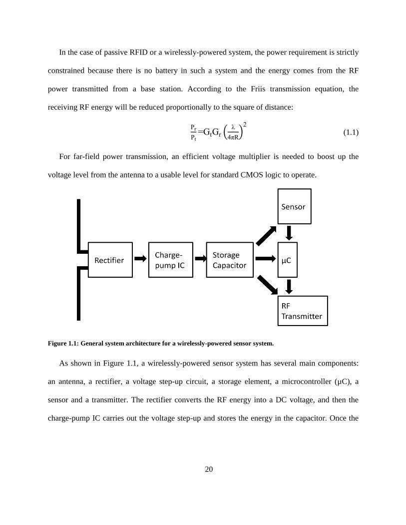
Figure 1.1: General system architecture for a wirelessly-powered sensor system.
As shown in Figure 1.1, a wirelessly-powered sensor system has several main components:
an antenna, a rectifier, a voltage step-up circuit, a storage element, a microcontroller (µC), a
sensor and a transmitter. The rectifier converts the RF energy into a DC voltage, and then the
charge-pump IC carries out the voltage step-up and stores the energy in the capacitor. Once the

21
voltage of the capacitor is sufficiently high, the microcontroller and other electronics will start to
operate. The detailed function of each block will be discussed in the following chapters.
Several papers on low-power microwave frequency voltage multipliers have been presented
using custom ICs or Schottky diodes [13, 14, 24]. One approach is a hybrid system consisting of
a thin lithium battery to power up the power converter for efficient RF energy harvesting in a
way that there is no need for battery replacement [5, 6]. It has been reported that the system can
harvest RF energy down to 1 µW level [5]. However, a thin film battery is needed for the system
to operate as shown in Figure 1.2. The drawback of having a battery is that extra circuitry is
needed to perform the voltage step-up to the specific voltage and energy is lost during the
process. The lifetime of the battery is another issue, and so this type of hybrid RF/battery system
is not considered in this thesis.
The other approach is a passive wirelessly-powered system without a battery and all the
energy is scavenged from the RF energy emitted from a base station [11, 13, 14, 16]. An
example of such a system utilizes 450 MHz for receiving the RF power and 2.3 GHz for the
transmitting the signal back to the base station [25]. A lower input frequency does offer longer
distance according the Friis free space equation. However, a 450 MHz antenna can be too big for
body-worn sensor applications. A similar system using a 1 W 915 MHz RFID reader for sensing
neural signals from an insect with a 1-metre range has been presented [14]. The RFID back-
scattering technique used here has the advantage that one antenna is needed for both receiving
RF energy and transmitting the sensor signal from and to the base station. However, the size of a
915 MHz antenna is still relatively big compared to the entire wirelessly-powered system itself.

22
A more recent 2.4 GHz wirelessly-powered glucose sensor in a contact lens as shown in Figure
1.3 has a size advantage of being smaller when compared to other lower frequency systems [13].
Figure 1.2: The 2.4 GHz wirelessly powered sensors system from the University of Colorado [6].
Figure 1.3: The 2.4 GHz wirelessly-powered glucose sensor in a contact lens from the University of
Washington [13].
The antenna is an essential component not only affecting the overall size of the wirelessly-
powered system but also the power efficiency and sensitivity of the system. There are many
different types of antennas suitable for this application including monopole, dipole, patch, and
spiral antennas [11, 14, 26]. The limitation of a linear polarized antenna such as a dipole is that

23
the orientations of both the transmitting and receiving antennas have to be aligned perfectly for
maximum power efficiency. Otherwise there will be energy loss due to polarization mismatch.
This requirement can be a problem in reality when the orientations of both antennas are unknown
or changing over time such as the orientation of a body-worn antenna is changing over time due
to body movement. One solution is using a dual-polarized patch antenna to receive energy from
both orthogonal polarizations [5, 27, 28]. An example of such a system is shown in Figure 1.4a.
Since the antenna can receive energy from an arbitrary polarization, there is no limitation on the
orientation of the antenna pair. However, since the feed lines are on both edges of the antenna,
the rectifier and matching network are needed to be duplicated on each edge [5, 8].
Figure 1.4: a) The integrated dual polarized patch antenna with rectifiers on both edges, b) Spiral antenna
array [5, 8].
Another approach resolving the polarization mismatch between antenna pairs is to adopt a
circularly-polarized antenna such as a spiral antenna [8]. With circular polarization the
electromagnetic wave is constantly rotating in a clockwise or counter-clockwise direction and so
(a) (b)

24
the polarization mismatch can be minimized if both transmitting and receiving antennas are
circularly-polarized in the same direction. An array of spiral antennas and rectifiers has been
built for ambient RF energy harvesting as shown in Figure 1.4b [8]. A circularly-polarized
antenna has potential to be an efficient antenna for low power transmission and this will be
discussed in more detail in Chapter 3.
The materials for the antenna are not limited to a traditional circuit board or ceramic
substrate. Textile antennas have been a growing area of interest for body-worn antenna
applications due to its light weight and ease of integration into clothing [29-35]. However, it is a
challenge to design a robust textile antenna for use on a human body due to the coupling between
the body and the near field of the antenna and this will be discussed in more detailed in Chapter
4 [36-38]. Therefore, this idea can be applied to a body-worn wirelessly-powered sensor system
and a working system on a human body will be demonstrated in Chapter 4 and 5.
1.2 Research Objective
The main objective of this thesis includes the followings:
Design a highly power sensitivity rectifier using off-the-shelf components.
Design a novel wideband circularly-polarized antenna on a single-sided circuit board.
Design a novel wideband circularly polarized textile antenna as a power receiving
antenna on a wearable wirelessly-powered sensor system.
Use very low microwave power to wirelessly power a temperature sensor system on a
human arm over a metre range.
However, there are several issues and areas are not addressed in this thesis:

25
Despite a high performance wearable textile antenna is developed for the wirelessly-
powered system in Chapter 4, the power transmission is impossible when the incoming
electromagnetic wave is 90° to the z-axis of the power receiving antenna. However, this
problem can be resolved using multiple antennas at different areas of a human body to
widen the power receiving area coverage [31, 33].
In Chapter 2 and 5, the highly power sensitive wirelessly-power systems are developed
using discrete components only and the designs are not further improved and
implemented in a CMOS integrated chip. This is because the emphasis of this thesis is on
the design of a novel textile antenna for a wirelessly-powered system and is not on the
system itself. The purpose of designing such a system is to demonstrate the effectiveness
of power transmission using the novel textile antenna developed in Chapter 3 and 4.
All the tests and measurements are carried out inside an anechoic chamber, therefore the
effect of multipath or interference due to reflections or from the environment is not
considered in this thesis.
1.3 Thesis Organization
The thesis is divided into 5 sections. The operation of the RF-DC conversion of the
microwave rectifier will be first introduced. Then the design of the wideband circularly-polarized
wide-slot antenna will be discussed. Later the wearable textile antenna for power transmission
will be developed. The application of the textile antenna on the wirelessly-powered sensor
system is then demonstrated and finally future plans will be discussed.

26
1.3.1 Microwave Rectifier
The RF energy is obtained from a base station and then it is transmitted through the antenna
to the microwave rectifier, where the RF-DC conversion is carried out. A zero-bias and highly
efficient Schottky diode is used in the design. Several different diode configurations have been
simulated and the prototypes are built on FR-4 for measurement in the laboratory. In Chapter 2,
the design methodology for a highly efficient microwave rectifier using the circuit optimizer
inside the Microwave Office (MWO) is presented. The power sensitivity and efficiency are
measured and compared to the other designs.
1.3.2 Antenna Design
In Chapter 3, a wide-slot wideband circularly polarized antenna is developed. This type of
antenna has the essential characteristics such as wide impedance and 3-dB axial ratio bandwidth
that are required for a flexible textile antenna for body-worn applications in the later chapters.
The objective is to understand and design a circularly polarized antenna with a single layer of
metal on a FR-4. The simulation is optimized using Microwave Office and CST and the
prototype is built and measured in an anechoic chamber. The result is compared with standard
circularly polarized patch antennas.
1.3.3 Textile Antenna for on-Body Application
In Chapter 4, the wide-slot antenna design from Chapter 3 is adopted and modified to become
a wearable textile antenna. The textile antenna is hand–made using a conductive fabric and self-
adhesive felt. The textile antenna is first simulated and measured without the consideration of a
human body, and then the simulation model considers the proximity of a human body to closely

27
match reality. The effect of bending and distance from a body are considered and measured in
the anechoic chamber.
1.3.4 A Sensor Platform with a Wearable Circularly Polarized
Textile Antenna
As the energy is scavenged using the rectenna (Rectifying Antenna), a charge-pump IC is
used to step up the voltage to 2.4 V for the microcontroller and sensor to operate. However, due
to the very low voltage requirement (0.3 V), the conventional DC-DC converter is not functional
at this voltage level. To solve this problem, a Seiko charge-pump IC is used to carry out this
function and this enables the wirelessly-powered sensor system to operate at an ultra-low input
RF power level (27 µW). In Chapter 5, a complete workable system will demonstrate how to
scavenge weak RF energy using the textile antenna and transforms the energy into the required
voltage for the microcontroller to sense the temperature and send the data back to the base
station.
1.3.5 Conclusion and Future Work
In Chapter 6, the conclusion will be drawn and the possible directions for future projects will
be discussed.
1.4 Conclusion
After brief discussion of the current development on wirelessly-powered technology, the
basic concept has been introduced. Therefore, the design detail of each building block will be
investigated in the coming chapters in order to build a low-power body-worn sensor system.

28
Chapter 2: Microwave Rectifier
2.1 Introduction
In this chapter, the simulation and implementation of the microwave rectifier centred at 2.45
GHz will be discussed. It will start with the basic concept of large signal S11 and Harmonic
Balance (HB) simulation in AWR Microwave Office® (MWO) and then the model of the
microwave rectifier is drawn in schematic. The performance of several different diode
configurations will be compared. Next, the implementation of the designs on PCB is used to
verify the simulation result. At the end, the efficiency and power sensitivity of the design are
measured and analyzed and a complete rectenna system is tested in the anechoic chamber.
2.2 Recent Developments in Rectifier Design
The basic function of a microwave rectifier is to convert an RF signal into a DC voltage at
microwave frequency. As shown in Figure 2.1, the full sine wave AC signal goes into the diode,
and it only allows positive voltage larger than its forward bias voltage to get through and this is
typical half-wave rectifier behaviour.
Figure 2.1: Basic structure of a rectifier.

29
The main challenge of a wirelessly-powered system is that the receiving RF power is
attenuated rapidly over the distance in free space according to the Friis transmission equation.
Therefore the receiving RF energy is not only needed to be rectified, but also needed to be step-
up to the required voltage level to drive the electronics in the transponder. To enhance RF energy
harvesting over a long distance, a multi-stage voltage multiplier is normally used as shown in
Figure 2.2 and it can be implemented using a diode or diode-connected nMOS transistor [23, 24,
39]. A 36-stage floating-gate voltage multiplier has been proposed to reduce the threshold
voltage of the CMOS devices to improve the sensitivity working over 44 metres [24]. However,
with more stages of voltage multiplier, more energy will be lost in the diodes and so the power
efficiency will be degraded as it will be shown in this chapter.
Figure 2.2: Multi-stage voltage multiplier [39].
Another method for improving efficiency is proposed based on LC power-matching network
with a ground inductor and a floating capacitor to minimize the number of stages of the voltage
multiplier and hence reduce the power lost in the transistors as shown in Figure 2.3 [40].
However, this method is limited by the quality of the inductor in standard CMOS process.

30
Figure 2.3: Die photo with internal inductor and voltage multiplier circuit [40].
A further enhancement is proposed based on a microwave step-up transformer to improve the
power efficiency over the LC power matching network as shown in Figure 2.4. The step-up
transformer provides a higher input impedance compared to just a LC matching network and so
the input voltage is increased and hence the overall power efficiency is increased [41]. However,
its modified voltage multiplier can only generate differential DC voltage.
Figure 2.4: Step-up transformer to improve input impedance [41].
In order to minimize the power loss in the voltage multiplier circuit, one suggested that the
voltage step-up process should be done at a lower frequency instead of at a microwave frequency

31
as shown in Figure 2.5 [42]. Note that only the first stage rectifier is done at microwave
frequency and then the DC generated is used to switch on the oscillator for the charge-pump
circuit which operate at kHz range and hence the power efficiency is improved by 14% [42].
This circuit can be implemented easily using off-the-shelf components and the power efficiency
is comparable to CMOS as it will be shown in this chapter.
Figure 2.5: Improved voltage multiplier with a low frequency charge-pump circuit [42].
2.3 Rectifier Design
2.3.1 Choice of Diodes
PN junction diodes are commonly used for low frequency applications only due to the large
junction capacitance [43]. PIN diodes are widely used in switches in microwave systems.
However, its junction capacitance is still relatively large and it requires a forward bias current of
10-30 mA [43]. For energy harvesting application, the forward bias voltage must be very low for
efficient RF-DC conversion and so a zero bias Schottky detector diode is the best candidate.
Figure 2.6 shows the spice model of the Agilent HSMS-2850 Schottky diode [44].

32
Figure 2.6: Spice model and parameters of the Schottky Diode [44].
SPICE Parameters
Parameter Units HSMS-285x SMS7630
BV V 3.8 2
Cj0 pF 0.18 0.14
EG eV 0.69 0.69
IBV A 3.00E-04 1.00E-04
IS A 3.00E-06 5.00E-06
N 1.06 1.05
RS Ω 25 20
Vj V 0.35 0.34
XTI 2 2
M 0.5 0.4
Table 2-1: Spice parameters of the HSMS-285x and SMS-7630 Schottky Diodes [44, 45].
The most important parameter for matching is the junction capacitance Cj0 as shown in Table
2-1. For such a small value, the matching network must require an external inductor to
compensate the capacitance. The other choice of Schottky diode is the Skyworks SMS-7630

33
which requires a slightly lower forward bias voltage [45, 46]. The lower forward bias voltage
always yields better power sensitivity. The performance of the two diodes will be used in our
rectifiers and the measured results will be shown in the later sections. The SC-79 (or SOD-523
for HSMS-285Y) packaging for SMS-7630 is chosen due to lower package parasitics and
smaller footprint [46].
2.3.2 A Brief Background on Harmonic Balance Simulation
The Harmonic Balance (HB) method is a powerful technique for the analysis of high-
frequency nonlinear circuits such as mixers, power amplifiers, and oscillators. HB simulation is
frequency domain analysis. Unlike the time-domain simulator SPICE, it gives the transient
behaviour and the steady state solution. The motivation behind using HB simulation over the
transient simulator is the following:
The distributed elements (e.g. transmission lines) in microwave circuits can be
exclusively modeled and analyzed in the frequency domain which is very hard to do
accurately and quickly in SPICE-like simulator.
HB simulator can handle multi-tone analysis quickly of microwave circuits in the
frequency domain. However, this is very difficult to handle in the time-domain. Imagine
you have a 10 GHz carrier signal modulated with 1 MHz data. The time domain
simulator must follow the slow envelope for several cycles to determine the steady state
solution. In the other words, the time domain simulator must follow many cycles of the
carrier to maintain the accuracy. It is obvious that this process is very time consuming
and consumes a lot of computing resources or simply runs out of memory.
34
There are a lot of microwave circuit which have very high-Q, which means the transient
time can be very long. It is a time consuming to trace the whole transient response if only
the steady state solution is if concern.
Therefore, a HB simulator is used for our microwave rectifier simulation and optimization.
More detail on Harmonic Balance method can be found on the AWR web site [47].
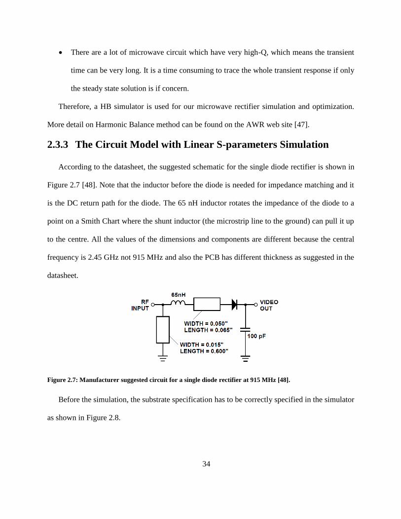
2.3.3 The Circuit Model with Linear S-parameters Simulation
According to the datasheet, the suggested schematic for the single diode rectifier is shown in
Figure 2.7 [48]. Note that the inductor before the diode is needed for impedance matching and it
is the DC return path for the diode. The 65 nH inductor rotates the impedance of the diode to a
point on a Smith Chart where the shunt inductor (the microstrip line to the ground) can pull it up
to the centre. All the values of the dimensions and components are different because the central
frequency is 2.45 GHz not 915 MHz and also the PCB has different thickness as suggested in the
datasheet.
Figure 2.7: Manufacturer suggested circuit for a single diode rectifier at 915 MHz [48].
Before the simulation, the substrate specification has to be correctly specified in the simulator
as shown in Figure 2.8.
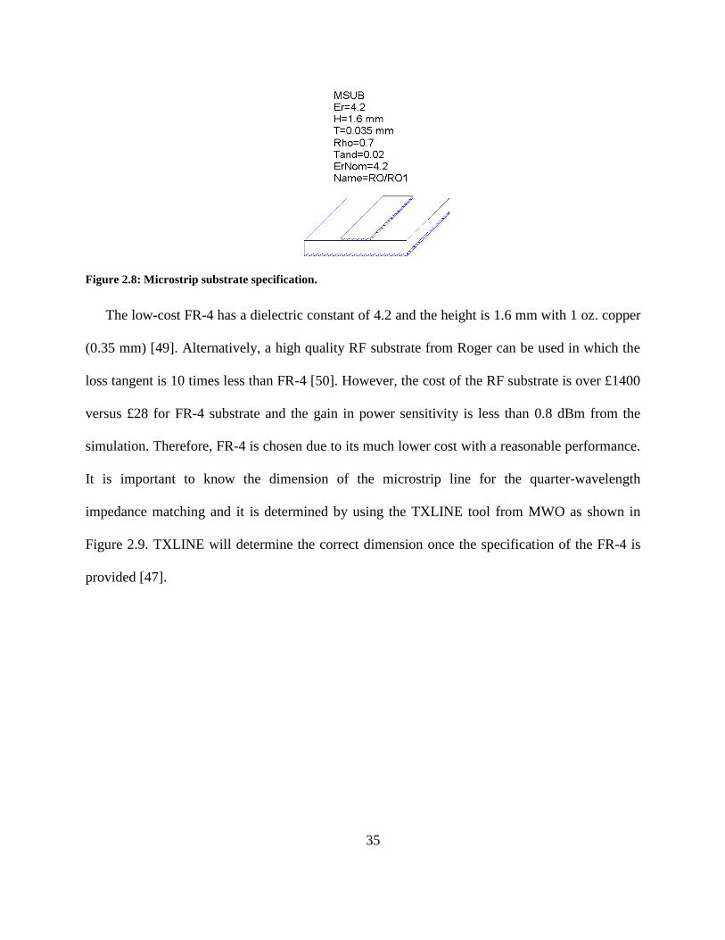
35
Figure 2.8: Microstrip substrate specification.
The low-cost FR-4 has a dielectric constant of 4.2 and the height is 1.6 mm with 1 oz. copper
(0.35 mm) [49]. Alternatively, a high quality RF substrate from Roger can be used in which the
loss tangent is 10 times less than FR-4 [50]. However, the cost of the RF substrate is over £1400
versus £28 for FR-4 substrate and the gain in power sensitivity is less than 0.8 dBm from the
simulation. Therefore, FR-4 is chosen due to its much lower cost with a reasonable performance.
It is important to know the dimension of the microstrip line for the quarter-wavelength
impedance matching and it is determined by using the TXLINE tool from MWO as shown in
Figure 2.9. TXLINE will determine the correct dimension once the specification of the FR-4 is
provided [47].

36
Figure 2.9: TXLINE is used to determine the quarter wavelength dimension of a microstrip line [47]. Note
that the name of the material can not be changed due to the limitation of the tool.
The model is constructed similar to the one from the datasheet and it is shown on Figure 2.10.
The optimizer is used to determine the right parameters for the schematic to achieve the S11 input
impedance matching and this provides good initial starting values for the more complicated
models as shown in Figure 2.11. Note that the simulation is carried out using a linear simulator
for a good initial guess and a more accurate result is obtained using nonlinear harmonic balance
simulation during the next section.
Note that the input matching can be done without any lumped elements by using a microstrip
alone [51, 52]. However, the footprint of the circuit will be significantly smaller using a chip
inductor and it is possible to keep the trace as short as possible for less energy loss.

37
Figure 2.10: Initial circuit model for a single diode rectifier.
Figure 2.11: Circuit optimizer for input impedance matching.
2.3.4 The Circuit Model with Harmonic Balance Simulation
As the concept of HB simulation has been discussed earlier in this chapter, HB simulation is
only concerned about the steady-state solution. In our application, since the AC to DC
conversion efficiency is at steady state, HB simulation is the best candidate for this purpose.
Therefore, the schematic for the single diode configuration with a HB input port (PORT_PS1)
for HB simulation is set up as shown in Figure 2.12. The lowest power of -14 dBm at 2.45 GHz
is specified. This is important because junction capacitance changes with input power level, and
the circuit optimization is based on this power level to obtain the best low power sensitivity of
the microwave rectifier. The package inductance and capacitance is modeled according to the
SDIODEID=Schotky1
8.143 mm
3 mm
16.61 nH 5 mm
200 pF
PORTP=2Z=50 Ohm
PORTP=1Z=50 Ohm

38
datasheet of the Schottky diode for better matching to the real circuit [46, 53]. An open circuit
/4 stub is also added at the cathode of the diode to short the fundamental frequency at the output
[51]. A 4.7 nH inductor is needed for the input matching with HSMS285 diode as a result. The
schematic for the SMS7630 is similar as shown in Figure 2.13.
Figure 2.12: The single diode rectifier circuit with a HSMS285 diode.
Figure 2.13: The single diode rectifier circuit with a SMS7630 diode.
1000 pF
0.5 mm
17.05 mm
1 2
3
4.992 mmSDIODEID=hsms285
1 nH1 nH
0.08 pF
4.7 nH
1.8 nH
1.8 nH
1
2
3
4
3.002 mm
1.5 mm0.7575 mm
3.011 mm
2 mm 1.2 nH PORTP=2Z=Rl Ohm
PORT_PS1P=1Z=50 OhmPStart=-14 dBmPStop=-6 dBmPStep=3 dB
500 pF
1.5 mm0.5 mm
18 mm
4 mm4.2 mm
4.7 nH
2.5 mm
1.5 nH
1 nH
0.08 pF
2 mm
2.2 nH
2.5 mm
1.5 nH
1 2
3
1
2
3
4
39
2.3.5 The Circuit Model of the Voltage Doubler and 4X Voltage
Multiplier
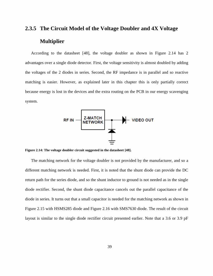
According to the datasheet [48], the voltage doubler as shown in Figure 2.14 has 2
advantages over a single diode detector. First, the voltage sensitivity is almost doubled by adding
the voltages of the 2 diodes in series. Second, the RF impedance is in parallel and so reactive
matching is easier. However, as explained later in this chapter this is only partially correct
because energy is lost in the devices and the extra routing on the PCB in our energy scavenging
system.
Figure 2.14: The voltage doubler circuit suggested in the datasheet [48].
The matching network for the voltage doubler is not provided by the manufacturer, and so a
different matching network is needed. First, it is noted that the shunt diode can provide the DC
return path for the series diode, and so the shunt inductor to ground is not needed as in the single
diode rectifier. Second, the shunt diode capacitance cancels out the parallel capacitance of the
diode in series. It turns out that a small capacitor is needed for the matching network as shown in
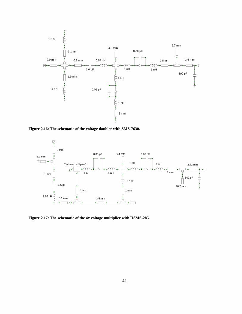
Figure 2.15 with HSMS285 diode and Figure 2.16 with SMS7630 diode. The result of the circuit
layout is similar to the single diode rectifier circuit presented earlier. Note that a 3.6 or 3.9 pF

40
capacitor is needed for the voltage doubler input matching as compared to an inductor which is
needed for single diode input matching, depending on which diode.
The same reasoning applies to the matching network of the 4X voltage multiplier as shown in
Figure 2.17 and the sub-circuit is shown in Figure 2.18 .The topology for the 4X voltage
multiplier is the Dickson multiplier and it is just a cascade of the 2 voltage doublers [39].
Therefore, the input matching topology is the same as the voltage doubler. Although the number
of stages can be increased by cascading more stage of the multiplier, but due to the loss of
energy in components and longer copper traces, there is no benefit using 8X voltage multiplier
and therefore it is not considered in this project. Note that the exact dimensions and component
values of each schematic are obtained by using the MWO Optimizer and it will be discussed in
the next section.
Figure 2.15: The schematic of the voltage doubler with HSMS-285.
1000 pF
5.6 mm
3 mm 0.5 mm
9.996 mm
3.9 pF
3.565 mm
12
3
SDIODEID=hsms285
1 nH 1 nH
0.08 pF
L=1 nH
1 nH
0.08 pF
0.1 nH
2 mm
1
2
3
4
2.662 mm
1.1 nH
4.068 mm
1.7 nH
1
2
3
4
3.09 mm
SDIODEID=hsms1
PORTP=2Z=Rl Ohm
PORT_PS1P=1Z=50 OhmPStart=-14 dBmPStop=-6 dBmPStep=3 dB
41
Figure 2.16: The schematic of the voltage doubler with SMS-7630.
Figure 2.17: The schematic of the 4x voltage multiplier with HSMS-285.
500 pF
6.1 mm2.9 mm 0.5 mm
9.7 mm
3.6 pF
3.6 mm
1 nH 1 nH
0.08 pF
1 nH
1 nH
0.08 pF
0.04 nH
2 mm
1
2
3
4
1.9 mm
1 nH
3.1 mm
1.8 nH
1
2
3
4
4.2 mm
12
3
500 pF
3 mm
1 mm
10.7 mm
2.73 mm
37 pF
1 mm
3.1 mm
1 nH
0.08 pF
1 nH
0.08 pF
3.5 mm
1 mm 1 mm
12
3
1
2
3
4
1 2
3
1 nH
1 nH
0.1 mm1.95 nH
1
2
3
0.1 mm
1.5 pF
12
3
1 2
3
"Dickson multiplier"

42
Figure 2.18: The Dickson multiplier sub-circuit within the 4X voltage multiplier.
2.3.6 Optimization and Simulation Results
In order to have the best efficiency from the microwave rectifiers, tuning of the S11 parameter
to be at least less than -10-dB at the centre frequency of 2.45 GHz is needed. The interface for
setting up the optimizer is shown in Figure 2.19 and the requirement of S11 parameter below -15
dB in the range of 2.4 GHz to 2.5 GHz is specified. The optimizer will tune the length of the
transmission line in the schematic to try to match the goal. The optimization is done individually
for each of the diode configurations.
Figure 2.19: Circuit optimizer in AWR MWO.
20 pF30 pF
1.316 mm
1.5 mm
SDIODEID=hsms285
SDIODEID=hsms1
1 nH
1 nH
0.08 pF0.08 pF
1
2
3
41 nH 1 nH
0.1 mmPORTP=1Z=50 Ohm
PORTP=2Z=50 Ohm
PORTP=3Z=50 Ohm

43
The optimized results are shown in Figure 2.20. There are 5 different rectifier circuits in this
figure: the voltage doubler with HSMS-2850, the voltage doubler with SMS-7630, the single
diode rectifier with HSMS-2850, the single diode rectifier with SMS-7630 and the 4x voltage
multiplier with HSMS-2850. Note that a 16 kΩ load resistor is chosen because this is an
approximation of the input resistance of the charge-pump IC for a voltage step-up from a
minimum of 0.3 V. It will be discussed more detail in Chapter 5.
Figure 2.20: The large signal S11 parameters for all different diode configurations.
As shown in Figure 2.20, S11 is matched to about -12 dBm on average only for the single
diode design because all the diodes are barely turned on with such a low voltage level and so
only a small amount of energy can get through the diode due to its built-in barrier.
The designs using the SMS-7630 show the best input matching due to a lower barrier, but the
difference is not significant when compared to the HSMS-2850. The S11 matching seems better
44
with voltage doublers and multipliers as their impedance is in parallel and so reactive matching
is easier, as stated in the datasheet. However, this doesn‟t mean more energy gets transferred to
the load because there is more energy loss in the diodes when compared to the single diode
configuration, as shown in the experimental results section later. Due to a mismatch between the
model and the circuit on the PCB, several iterations are made to match the model as close to the
circuit on PCB as possible. It is found that the ground connection for the matching stub is about
1 nH and it must be added in the model for the better accuracy to match the reality. With an
adjusted model, the S11 matching between simulation and measurement is very close with only a
small manual adjustment needed on the PCB to accommodate the process variation on each
design.
2.3.7 Manufacturing of the Rectifiers
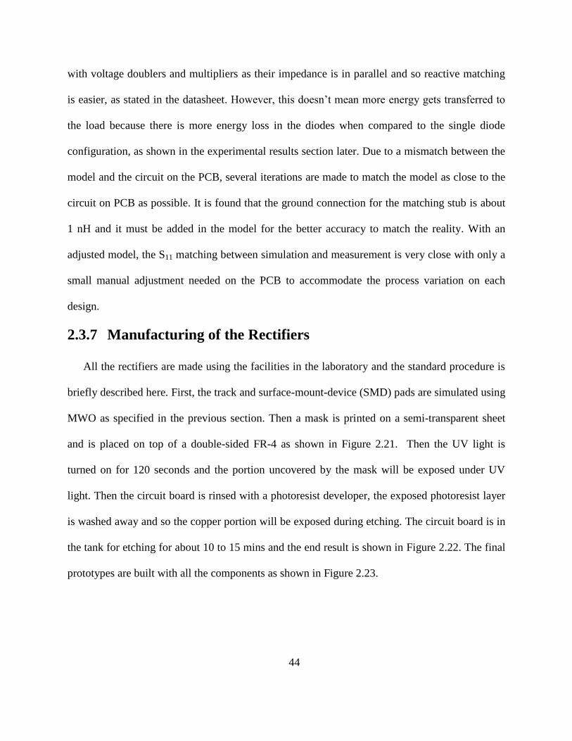
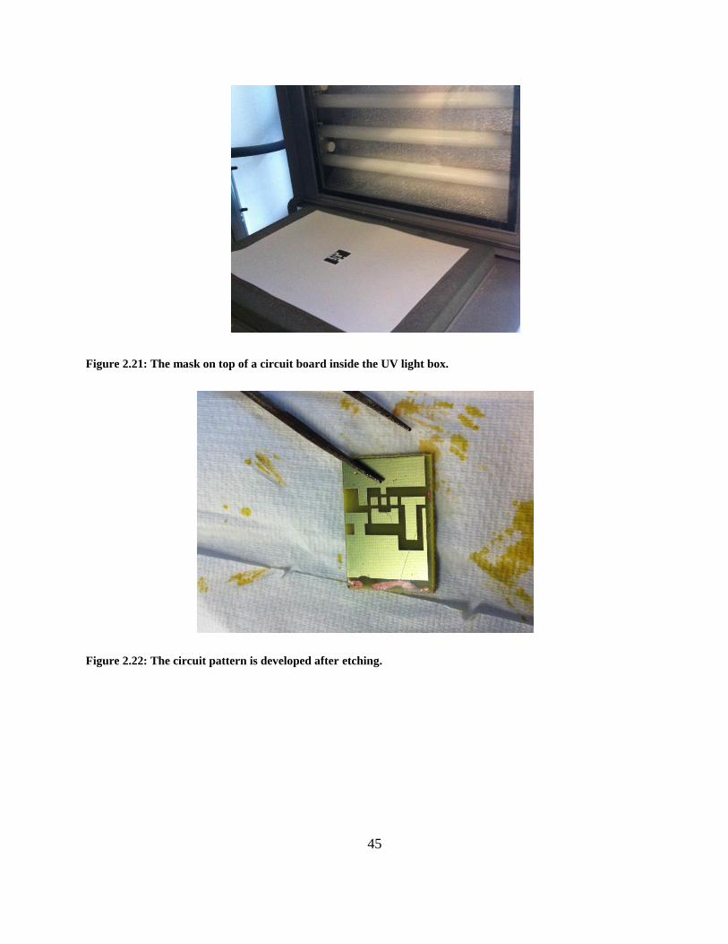
All the rectifiers are made using the facilities in the laboratory and the standard procedure is
briefly described here. First, the track and surface-mount-device (SMD) pads are simulated using
MWO as specified in the previous section. Then a mask is printed on a semi-transparent sheet
and is placed on top of a double-sided FR-4 as shown in Figure 2.21. Then the UV light is
turned on for 120 seconds and the portion uncovered by the mask will be exposed under UV
light. Then the circuit board is rinsed with a photoresist developer, the exposed photoresist layer
is washed away and so the copper portion will be exposed during etching. The circuit board is in
the tank for etching for about 10 to 15 mins and the end result is shown in Figure 2.22. The final
prototypes are built with all the components as shown in Figure 2.23.
45
Figure 2.21: The mask on top of a circuit board inside the UV light box.
Figure 2.22: The circuit pattern is developed after etching.

46
Figure 2.23: The 5 different rectifier designs. The top row from the left is the voltage doubler with HSMS-
2850, SMS-7630 and 4X voltage multiplier with HSMS-2850. The bottom row from the left is the single diode
rectifier with HSMS-2850 and SMS-7630
2.4 Experimental Results
2.4.1 Large Signal S11 Parameter Matching
The S11 parameters are measured using an Agilent E8361A PNA. Each circuit was manually
tuned to resonate at 2.45 GHz by iterating between the simulation and the measured results. For a
small degree of tuning, adjusting the length of the matching stub is needed. The measured S11
values are shown in Figure 2.24.

47
Figure 2.24: The S11 parameter measurements with -14 dBm signal power.
As shown in Figure 2.24, the voltage doubler always has better S11 matching than the single
diode design, no matter which diode is used. This is because the shunt diode provides clamping
for the series diode and so there is a DC voltage at the junction of the 2 diodes. This provides the
forward bias voltage for the series diode and so the RF signal can get through the barrier easier.
And so less energy gets reflected back, meaning the return loss is lower. However, though this
may imply that more power can go through the series diode and more RF power has been
converted to DC voltage for the load, this is not true for the voltage doubler. It is because a
portion of the energy is consumed in the shunt diode to provide the DC bias voltage of the series
diode, less energy gets transferred to the load, although the return loss is better than the single
diode design. This phenomenon is more apparent in the case of the 2-stage voltage multiplier as

48
even more energy is consumed in the diodes and traces on the PCB, resulting in far less energy
getting to the load for conversion into usable voltage.
2.4.2 Rectifier with a Microcontroller
The ultimate goal for building these rectifiers is to provide the power for the wirelessly-
powered sensor system as will be shown in the later chapters. It is important to understand the
power efficiency of the rectifier and also the efficiency of the overall system with each input
power level.
Each rectifier is connected to an R&S model SML 03 signal generator directly and then the
minimum input power levels required for the voltage multipliers to turn the microcontroller (µC)
on to flash the LED without the Seiko charge-pump IC is measured as shown in Figure 2.25 and
the results are summarized in Table 2-2.
Figure 2.25: The single diode rectifier with the µC connected to the signal generator.
The single diode rectifier and voltage doubler with HSMS-2850 require 1.0 dBm and -0.4
dBm input power to turn on the µC, respectively. While the single diode rectifier using SMS-

49
7630 requires only 0.7 dBm, the voltage doubler requires only -2.3 dBm. When using the
HSMS-2850, the voltage doubler produces a 1.4 (1+0.4) dBm improvement on the power
sensitivity and the voltage sensitivity is improved from 250.9 mV to 213.5 mV over the single
diode rectifier configuration. The voltage doubler with SMS-7630 delivers 3.0 dBm power
sensitivity improvement over the single diode design and the voltage sensitivity is improved
from 242.4 mV to 171.6 mV. This result is due to the measured forward bias voltages of the
HSMS-2850 and SMS-7630 being 0.18 V and 0.16 V, respectively. The advantage is the lower
forward bias voltage is doubled when the diodes are in the voltage doubler configuration and this
results in a 41.9 mV voltage sensitivity improvement using SMS-7630 versus HSMS-2850. The
4X voltage multiplier with HSMS-2850 requires -2.1 dBm to turn the µC on. It exhibits a 1.7
(2.1- 0.4) dBm improvement over the voltage doubler and the input voltage sensitivity is very
close to that of the voltage doubler with SMS-7630. The addition of an extra stage results in a
less than 2 dBm improvement for input power sensitivity. Furthermore, there appears to be no
advantage using a 3-stage voltage multiplier in the simulation as the impedance match is harder
to achieve and power loss in the components and PCB is greater.
Different microwave
rectifiers with the µC
Single
diode
(HSMS-
2850)
Single
diode
(SMS-
7630)
Voltage
doubler
(HSMS-
2850)
Voltage
doubler
(SMS-
7630)
4X Voltage
multiplier
(HSMS-
2850)
Minimum required
input power to turn on
the µC to flash the LED
1 dBm 0.7
dBm
-0.4 dBm -2.3 dBm -2.1 dBm
Table 2-2: Measured minimum input power to turn on the µC to flash the LED for the different rectifier
designs.
50
2.4.3 Rectifier with a Charge-Pump IC and a Microcontroller
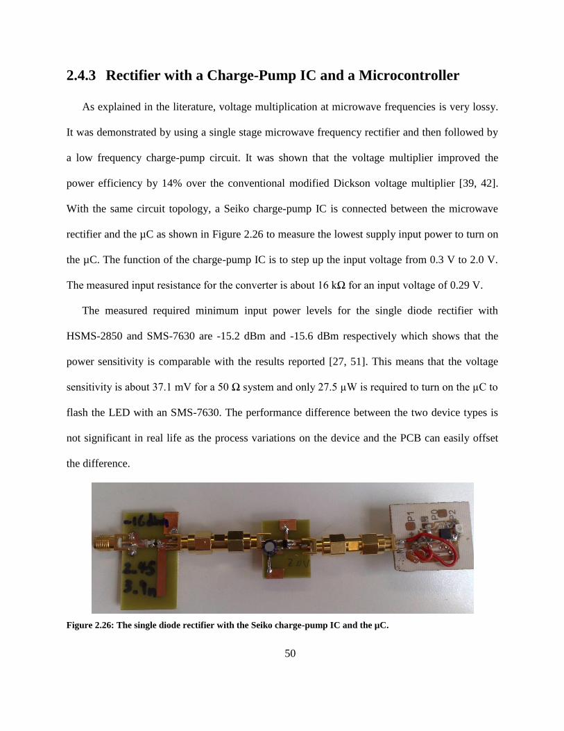
As explained in the literature, voltage multiplication at microwave frequencies is very lossy.
It was demonstrated by using a single stage microwave frequency rectifier and then followed by
a low frequency charge-pump circuit. It was shown that the voltage multiplier improved the
power efficiency by 14% over the conventional modified Dickson voltage multiplier [39, 42].
With the same circuit topology, a Seiko charge-pump IC is connected between the microwave
rectifier and the µC as shown in Figure 2.26 to measure the lowest supply input power to turn on
the µC. The function of the charge-pump IC is to step up the input voltage from 0.3 V to 2.0 V.
The measured input resistance for the converter is about 16 kΩ for an input voltage of 0.29 V.
The measured required minimum input power levels for the single diode rectifier with
HSMS-2850 and SMS-7630 are -15.2 dBm and -15.6 dBm respectively which shows that the
power sensitivity is comparable with the results reported [27, 51]. This means that the voltage
sensitivity is about 37.1 mV for a 50 Ω system and only 27.5 µW is required to turn on the µC to
flash the LED with an SMS-7630. The performance difference between the two device types is
not significant in real life as the process variations on the device and the PCB can easily offset
the difference.
Figure 2.26: The single diode rectifier with the Seiko charge-pump IC and the µC.

51
The minimum required input power levels for voltage doublers using HSMS-2850 and SMS-
7630 are -13.8 dBm and -15.5 dBm, respectively. It is clear from this that the voltage doubler
does not have any advantage over the single diode rectifier when operated with the charge-pump
IC. The 4X voltage multiplier requires -12.3 dBm input power to turn on the µC and the results
are summarized in Table 2-3.
Different rectifiers
with Seiko charge-
pump IC and µC
Single
diode
(HSMS-
2850)
Single
diode
(SMS-
7630)
Voltage
doubler
(HSMS-
2850)
Voltage
doubler
(SMS-
7630)
4X Voltage
multiplier
(HSMS-
2850)
Minimum required
input power to turn
on the µC to flash
the LED
-15.2 dBm -15.6 dBm -13.8 dBm -15.5 dBm -12.3 dBm
Table 2-3: Measured minimum input power for different rectifier designs with a Seiko charge-pump IC.
Voltage is boosted in the voltage doubler but since energy has to be conserved, less current is
delivered to the load because of this. The rectifier has to provide sufficient voltage for the µC
and power for the charge-pump IC to operate. Therefore the choice of diode configuration
depends ultimately on the load resistance expected. The input resistances of the µC and the
charge-pump IC just before turn-on are about 60 kΩ and 16 kΩ, respectively. For a lower
resistive load, the single diode design is better because it can supply more current as long as the
voltage supplied is just enough to turn the chip on. For high resistive loads, the voltage doubler
or multi-stage voltage multiplier can perform better because the load draws less current.
However, impedance matching is easier with a voltage doubler and so it has advantages where
space is at a premium and the addition of a comparatively large microstrip matching stub would
not be permissible.

52
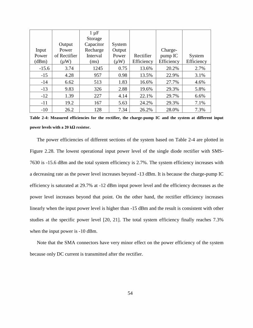
2.4.4 Power Efficiency
The efficiencies for the single diode rectifier with SMS-7630, the charge-pump IC and the
overall system at different power levels with load resistance 20 kΩ are measured and the results
are summarized in Table 2-4. The 20 kΩ load is chosen because the µC has similar input
resistance when it is turned on. The storage capacitor recharge interval represents the idle time of
the µC because the charge-pump IC takes time to charge up the 1 µF storage capacitor to 2 V. A
1 µF capacitor is chosen because it has relatively short charging time and it provides sufficient
energy for the operation of a µC in the next section. At the lowest operational input power level -
15.6 dBm, it takes the charge-pump IC about 1.2 seconds to charge up the capacitor to 2 V to
turn on the µC to flash the LED. However, at input power level -10 dBm, it only takes about 0.13
seconds to charge up the storage capacitor. The measurable efficiencies within the harvester are
defined as follows:
Rectifier Efficiency= Output Power from Rectifier
Primary Input Power 2.1)
Charge Pump IC Efficiency= Output Power from Charge Pump IC
Input Power to Charge Pump IC 2.2)
ystem Efficiency= Output Power from Charge Pump IC
Primary Input Power 2.3)
Note that although the output voltage level from the rectifier is continuous, the output voltage
level of the charge-pump IC is a short pulse as shown in Figure 2.27. Note that the voltage is
decreasing over time because the storage capacitor is discharging and the charge-pump IC will
shut down the connection when the voltage drops below the threshold. The trace C1 shows that
the separation of the output pulses from the charge-pump IC is about 1.2 seconds and it is

53
depending on the input power level. The trace Z1 shows that the pulse width is always about 6.6
ms because it is independent of the input power level. The charge-pump IC charges the storage
capacitor up to 2 V and then releases the energy until it drops to 1.4 V. Therefore, the voltage
output of the system is the following:
V t =2e-t 0.02 2.4)
where V(t) is the voltage output of the system. The RC time constant is 0.02 because of the 1µC
storage capacitor and 20 kΩ resistor. The average power output is calculated as below where T is
the period of the pulse and R is the load resistance:
P=1
TR V2 t dt
0.0066
0
=9.4
T mW .5)
Figure 2.27: Measured pulse separation and pulse width of the output of the charge-pump IC.
54
Input
Power
(dBm)
Output
Power
of Rectifier
(µW)
1 µF
Storage
Capacitor
Recharge
Interval
(ms)
System
Output
Power
(µW)
Rectifier
Efficiency
Charge-
pump IC
Efficiency
System
Efficiency
-15.6 3.74 1245 0.75 13.6% 20.2% 2.7%
-15 4.28 957 0.98 13.5% 22.9% 3.1%
-14 6.62 513 1.83 16.6% 27.7% 4.6%
-13 9.83 326 2.88 19.6% 29.3% 5.8%
-12 1.39 227 4.14 22.1% 29.7% 6.6%
-11 19.2 167 5.63 24.2% 29.3% 7.1%
-10 26.2 128 7.34 26.2% 28.0% 7.3%
Table 2-4: Measured efficiencies for the rectifier, the charge-pump IC and the system at different input
power levels with a 20 kΩ resistor.
The power efficiencies of different sections of the system based on Table 2-4 are plotted in
Figure 2.28. The lowest operational input power level of the single diode rectifier with SMS-
7630 is -15.6 dBm and the total system efficiency is 2.7%. The system efficiency increases with
a decreasing rate as the power level increases beyond -13 dBm. It is because the charge-pump IC
efficiency is saturated at 29.7% at -12 dBm input power level and the efficiency decreases as the
power level increases beyond that point. On the other hand, the rectifier efficiency increases
linearly when the input power level is higher than -15 dBm and the result is consistent with other
studies at the specific power level [20, 21]. The total system efficiency finally reaches 7.3%
when the input power is -10 dBm.
Note that the SMA connectors have very minor effect on the power efficiency of the system
because only DC current is transmitted after the rectifier.

55
Figure 2.28: Measured efficiencies of the rectifier, the charge-pump IC and the overall system.
The comparison of this work to the other monolithic power harvesters is shown in Table 2-5.
At 2.45 GHz, our power harvester performs as efficiently as the monolithic solution at -13.5
dBm. The RF sensitivity of our power harvester is -15.6 dBm and it is second best in the table
due to the combination of a highly efficient Schottky diode and an ultra-low input voltage Seiko
charge-pump IC. The 869 MHz monolithic design performs the best as the Schottky diodes are
integrated in the chip and lower electromagnetic loss at the lower frequency. However, the size
of an 869 MHz antenna is much bigger than a 2.45 GHz counterpart [23]. The output voltage of
our power harvester is the highest in the table and it can be as high as 2.4 V by using a different
model of the charge-pump IC [54]. With this output voltage, our power harvester can easily
power up any general purpose µC, sensors and RF transceiver.
In general, an integrated CMOS chip has size and power advantages over the discrete
component design such as for a biomedical implanted device where the size is strictly limited.
13.6%
26.2%
2.7%
7.3%
20.2%
28.0%
0.0%
5.0%
10.0%
15.0%
20.0%
25.0%
30.0%
-16 -15 -14 -13 -12 -11 -10
Eff
icie
ncy
Input Power Level (dBm)
Rectifier Efficiency Total System Efficiency
Charge-pump IC Efficiency

56
An integrated CMOS chip also has a cost advantage over discrete component design if it is
produced in a large quantity. However, for the purpose of this thesis, only a few prototypes are
needed to test out the idea in a very short turn around time and to test the effectiveness of the
specialized antennas developed in Chapter 3 and 4 for low power transmission. Therefore, a
discrete component design is more suitable to serve the purpose.
References This work [55] [23] [41] [40] [23]
Frequency 2.45 GHz 2.45 GHz 3.85 GHz 920 MHz 869 MHz
Sensitivity
(dBm)
-15.6 -13.5 -12.0 -14.1 -19.0
Maximum
Output
Voltage
2 1.5 1 1 1.5
System
Efficiency
6.5% @ -12 dBm
5.7% @ -13 dBm
4.6% @ -14 dBm
2.7% @ -15.6 dBm
5%@
-13.5 dBm
1.0%@
-12 dBm
5.1%
@
-14.1dBm
18%
@ -19 dBm
Fabrication
Process
discrete
components on
FR-4
0.5µm
CMOS+
Schottky
Diodes
0.18µm
CMOS
0.18µm
CMOS
0.5µm
CMOS+
Schottky
Diodes
Table 2-5: Performance comparison of different power harvesters.
2.4.5 Range Test for the Transponder
Instead of using a resistor in the previous section, a µC is connected to the system to verify
the functionality of the whole wirelessly-power system. Lastly, the single diode rectifier with an
SMS-7630 is incorporated to make a full rectenna system using simple FR-4 patch antennas
attached to the R&S signal generator and rectifier circuit individually. With an RF power
amplifier attached to the signal generator, it can radiate a total of 18.8 dBm (0.097 W) after
power losses in the cabling to the anechoic chamber. The charge-pump IC and microcontroller
are attached to the rectifier as shown in Figure 2.29.

57
Figure 2.29: The rectenna with 2.45 GHz patch antenna, the rectifier, Seiko IC and the microcontroller.
With this setup, the longest operational distance is measured from the antenna of the signal
generator to the rectenna, as shown in Figure 2.30. The measured longest distance is 57
centimetres. Based on these measurements, according to the Friis transmission equation, 1W of
transmitting power can easily power up the receiver over a 1 metre range.
Figure 2.30: The wirelessly-powered system inside the anechoic chamber for the measurement
2.5 Conclusion
The design of the highly power sensitive rectifier is constructed and able to demonstrate
powering up the wirelessly-powered platform at 2.45 GHz using discrete components on a
conventional FR-4 circuit board over a distance of 0.57 metres with just 100 mW and its
performance is comparable to custom CMOS solutions with the help of the charge-pump IC. The

58
above work lays down a foundation building block for a low-cost and ultra-low-power battery-
less wearable sensor platform which will be as shown in Chapter 5.
However, using a linear polarized patch antenna for power transmission as shown here has a
very restricted limitation on the antenna orientation. As for a body-worn wirelessly-powered
system, the human body is not always perfectly aligned to the power sourcing antenna at the base
station. For example, if the antenna at the base station is in a vertical position and the antenna at
the human body is in a horizontal position, the efficiency of the power transmission will be
significantly degraded. Therefore, in the next chapter a better type of antenna topology is
introduced to address this issue.

59
Chapter 3: Antenna Design
3.1 Introduction
In this chapter, a wideband wide-slot antenna topology will be introduced for robust off-body
wireless power transmission. First, a standard linearly-polarized patch antenna is briefly
described and then various methods to generate circular polarization are discussed. However, due
to the bandwidth limitation or geometric complexity of a circularly-polarized (CP) patch
antenna, it can be a problem when creating a low cost and simple body-worn antenna for
microwave power transmission. Therefore, a simple wide-slot antenna topology is proposed to
address this issue. The simulation shows that it has very wide impedance and axial ratio
bandwidths when compared to a patch antenna. Finally, the performance of the antenna on FR-4
is measured and discussed.
3.2 Antenna Characteristics
Before designing a high performance antenna for the specific application, some important
parameters have to be defined and then optimized during simulations.
3.2.1 Bandwidths
Bandwidth is defined as the frequency range that the antenna performs at an acceptable level
[56]. There are two bandwidths that are of most concerned in this chapter for designing an
antenna: impedance and axial ratio bandwidths. Impedance bandwidth is defined as the
frequency range that the antenna can still maintain good impedance matching and having S11 less
than -10 dB is commonly considered as a good impedance matching at the present time [56, 57].
The axial ratio bandwidth is defined as the frequency range that the antenna is radiating in

60
circular polarization and an axial ratio with less than 3-dB is considered as good polarization
purity in practice [26, 56, 58, 59]. The definition of axial ratio will be discussed in the later
section.
3.2.2 Polarization
Polarization is defined as the orientation of the electric field coming from an antenna and it
can be linear, circular or elliptical [56]. This is an important characteristic of an antenna as the
polarization between the transmitting and receiving antennas has to match for them to
communicate effectively. For example, a vertically polarized antenna cannot communicate with
a horizontally polarized antenna. In a similar fashion, a circularly polarized antenna can only
receive half of the power from a linear polarized transmitting antenna due to polarization
mismatch [56].
Circular polarization can be left-handed circular polarization (LHCP) or right-handed circular
polarization (RHCP) depending on the direction of the rotation of the electric field [56].
However, in reality circular polarization is difficult to achieve perfectly and in most cases it
behaves as elliptical polarization with unequal orthogonal components in the electric field [56,
60, 61].
3.2.3 Axial Ratio
Axial ratio is a measure of the purity of the circular polarization of an antenna and it is
defined as the absolute value of the sum of the electric fields divided by the difference of the
electric fields from both polarizations and it is also defined by the ratio of the major axis to the
minor axis of the polarization ellipse [31, 47, 56]:

61
Axial ratio = 20log ERHCP E HCP
ERHCP-E HCP = 20log
EMax
EMin (3.1)
where ELHCP and ERHCP are the LHCP and RHCP electric field, respectively and Emax Emin are the
major axis and minor axis of the polarization ellipse, respectively.
An axial ratio of 0-dB means that the polarization is perfectly circular. In reality, perfect
circular polarization is hard to obtain and the so the axial ratio is usually bigger than 0-dB and 3-
dB is currently considered as a good polarization purity in the antenna community. Therefore, 3-
dB axial ratio bandwidth is commonly used as a figure of merit for the polarization performance
of an antenna in most literature [59, 62-64].
3.2.4 Antenna Gain
Antenna gain is defined as the power of the radiation as a function of angles compared to an
isotropic source and it is a function of efficiency and directivity [1, 56, 65]. A typical gain for a
patch antenna is around 3-5 dBi due to variations of geometry and power loss in the material of
the antenna [56].
3.3 Choices of Antennas
There are many types of antennas such as monopole, dipole, loop, horn, spiral, helical and
patch antennas [65]. Monopole and dipole antennas are easily made using a simple wire and they
are good choices for a transmitter radiating in all directions. However, the gain of a /2 dipole is
only 2.15 dBi and a monopole requires a ground plane that the whole structure will become 3-
dimensional. A 1 loop antenna has a similar gain to a /2 dipole and a large loop antenna has
relatively high gain but it has a very large radiation resistance that makes input impedance
matching difficult [65]. Horn and helical antennas have high gains and wide bandwidths, but the

62
physical sizes are too big to be portable. A patch antenna has higher gain than a dipole, but the
bandwidth is very narrow. However, due to its simple planar structure, it can be manufactured
with a standard etching processing for PCB. Therefore, it has been widely used in the industry
such as mobile phones [56]. Due to its planar structure, it can be easily integrated into textile and
so there is a growing interest to use wearable textile patch antennas for on-body communication
[31, 66, 67].
3.4 Basics of a Patch Antenna
Microstrip or patch antennas are widely used in commercial applications because they are
cheap, compact in size and easy to fabricate on a PCB using standard etching process [49]. A
typical rectangular patch antenna is shown in Figure 3.1. A rectangular patch basically consists
of a conductive patch and a ground plane with a dielectric in between. A patch is a piece of metal
with length L and width W sitting on top of a substrate (circuit board) with height h:
Figure 3.1: A standard linear polarized patch antenna.
The frequency of operation is determined by the length of the patch and is approximately
given by this equation [56]:

63
f =c
2 r 3.2)
where c is the speed of light, L is the length of the patch antenna and r is the relative dielectric
constant. The width W controls the input impedance and radiation pattern. The permittivity r
controls the fringing field which will affect the radiation efficiency. The directivity of patch
antennas is approximately 5 dBi and the fields are linearly polarized.
3.5 Patch Antenna Feeding Techniques
There are many ways of feeding a patch antenna such as probe feed, inset feed, quarter-
wavelength transformer feed and proximity feed. We will provide the brief background
information of inset and proximity feedings in the following sections [68].
The first type of feed is an inset feed and since the edge of the patch antenna has high
impedance, in order to match the 50 Ω line, the feed line goes toward the centre of the patch for
lower input impedance as shown in Figure 3.2a. The exact match needs to be done
experimentally on the length and the inset notch size [56]. The advantage of this feed is ease of
fabrication as since it is a single layer it requires only standard etching process. The only
disadvantage is that it requires manual tuning for the length of the inset and it suffers from
spurious radiation from the feed line.
The second type of feed is when the feed line is not physically touching the patch antenna as
shown in Figure 3.2b. The energy is radiated from the feed line to the patch through the
substrate. But coupling exists between the feed line and the patch and this gives you extra
freedom for tuning. The advantage is that it offers extra effective substrate thickness, and it will

64
give better radiation due to an increase of the fringing field. The disadvantage is that multilayer
fabrication is required which means high cost of manufacturing.
The third type of feed is using a quarter-wavelength transformer to provide the impedance
matching between a 50 Ω transmission line to the edge impedance of a patch antenna which is
typically around 200 Ω as shown in Figure 3.2c. The disadvantage is the radiation pattern is
slightly affected due to disturbance of the one radiating edge and it takes extra space for the
transformer.
The fourth type of feed is a coaxial feed in which a transmission line directly feeds to the
patch through the ground plane as shown in Figure 3.2d. The metal is removed from the ground
plane to leave the space for the outer shield of coaxial line. This method provides the purest
radiation pattern from all the above methods. But the disadvantage is that it requires drilling and
locating the optimum 50 Ω point for feeding which in turn requires manual tuning.
Figure 3.2: (a) Inset feed, (b) Proximity feed, (c) Quarter-wavelength feed, (d) Coaxial feed.
3.6 Wideband Patch Antenna
A linearly-polarized microstrip patch antenna is great for its low cost, high gain and easy
manufacturing on a printed circuit board. However, a standard patch antenna has a typical
limited bandwidth of less than 4% on a FR-4 board and so the resonant frequency can be shifted

65
due to manufacturing variations [56]. This will degrade significantly the performance of the
microwave power transmission in the wirelessly-powered system. There are numerous ways to
increase the impedance bandwidth of a patch antenna which involves: a) impedance matching
network [56], b) increase the volume of the antenna such the thickness of the substrate [56], c)
multiple feed-points [68] and d) variations of antenna geometry to introduce extra resonant
frequencies [69]. It has been reported that the impedance bandwidths can go up to 32% and 69%
at centre frequencies 2.4 GHz and 7.7 GHz, respectively [70, 71]. Some examples of these
wideband patch antennas are shown in Figure 3.3. However, these structures would be too
complicated to implement on a flexible substrate such as conductive textile as it may be bent on
a human body as shown in the next chapter and so the performance will be degraded.
Figure 3.3: Examples of the wideband patch antennas [70, 71].
3.7 Circularly-Polarized Patch Antennas
In order to deliver robust power transmission to a human body, circular polarization is
preferred due to the independence of orientation between the antenna pair. Therefore, a wide
band circularly-polarized antenna structure is desirable for such an application. A standard patch

66
antenna can generate circular polarization by doing: a) diagonal feed point, b) cutting off corners
or c) feeding with a 90° branchline hybrid. These methods can offer 3% to 20% 3-dB axial ratio
bandwidths [72, 73]. However, a 3-dB axial ratio bandwidth can be up to 34% at centre
frequency of 1.8 GHz using dual feeds and it can be as high as 81% using 4 feed lines at centre
frequency of 1.5 GHz with 3-dimensional feeding structure as shown in Figure 3.4 [74, 75].
Figure 3.4: Example of the wide 3-dB axial ratio bandwidth antenna with multiple feed lines [74].
However, this multiple feed structure can be difficult and costly to implement on a
conductive textile and the 3-dimensional feeding structure which is not resistant to bending due
to body movement. The precise spacings within the structure are difficult to maintain under
stress if the design is implemented on a flexible textile. Therefore, it is preferred to have a single
fed planar design and at the same time featuring wide band circular polarization for the body-
worn antenna that will be introduced next.
3.8 Wide-Slot Antenna
Recently, CP antennas have been getting more attention from the wireless community where
the traditional patch is adapted by including notches or choosing the feed point along the
diagonal of the patch with limited bandwidth as mentioned earlier. However, a simple geometry

67
and single layer square slot antenna can easily outperform standard CP patches but with lower
cost as shown in Figure 3.5 [76].
Figure 3.5: Example of a wideband CP wide-slot antenna [76].
The advantage of a wide slot antenna is that the geometry is very simple and it doesn‟t
require an extra layer for a ground plane while it features wide impedance bandwidth compared
to a patch antenna. The cost saving can be significant if a large array of antennas is needed for
higher gain. The physical size can be more compact without a ground plane and it implies that it
can be seamlessly integrated into clothings for body-worn textile antennas. There is a significant
bandwidth advantage of the wide-slot antenna over a standard patch antenna with a just single
layer of metal and substrate as shown in the later section. An impedance bandwidth of 110%
with centre frequency of 3.5 GHz and 3-dB AR bandwidth of 85% has been recently reported
using a single sided FR-4 substrate [77]. The missing ground plane means lower cost for
manufacturing, but it also implies that the radiation can go in both the front and the back

68
directions. However, this is not a problem as the antenna is used as a passive device to absorb
microwave energy from a base station as shown in Chapter 1. The coupling to the body will
significantly affect the antenna performance, but as shown in the next chapter this is not a
problem once the distance between the antenna and body is at a reasonable distance and the gain
of the antenna is even amplified due to body reflection.
The frequency of operation is determined by the length of the slot and is approximately given
by this equation [56]:
fr 300
W r,eff, r,eff=
2 r
1 r. (3.3)
In this empirical formula, fr is the resonant frequency of the fundamental mode in GHz, L
and W are the inner width and length of the slot in millimetres and r, eff is the effective dielectric
constant.
3.8.1 Wide Slot Antenna Feeding Techniques
There are two common feeding methods for a wide slot antenna which are microstrip line
feed and coplanar waveguide (CPW) feed as shown in Figure 3.6a and b. The advantage of the
microstrip line feed is that there is more freedom on the shape of the slot and feed line as they
can overlap but on different layers [63, 78-82]. However, the disadvantage is that it requires an
extra metal layer as the slot and the feed are on the opposite sides of the substrate. The other
method is using a CPW feed which has the advantage of using only 1 layer of metal as there is
no ground plane for a wide slot antenna [59, 77, 83-86]. However, the disadvantage is there is
more constraint on the shape of the feed line and the slot as they cannot overlap and the gap in
the waveguide has to be small to match to 50 Ω. Even with these disadvantages, a CPW feed
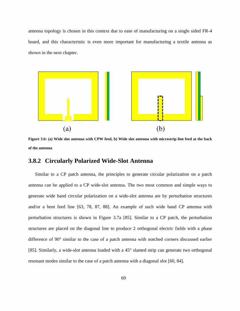
69
antenna topology is chosen in this context due to ease of manufacturing on a single sided FR-4
board, and this characteristic is even more important for manufacturing a textile antenna as
shown in the next chapter.
Figure 3.6: (a) Wide slot antenna with CPW feed, b) Wide slot antenna with microstrip line feed at the back
of the antenna
3.8.2 Circularly Polarized Wide-Slot Antenna
Similar to a CP patch antenna, the principles to generate circular polarization on a patch
antenna can be applied to a CP wide-slot antenna. The two most common and simple ways to
generate wide band circular polarization on a wide-slot antenna are by perturbation structures
and/or a bent feed line [63, 78, 87, 88]. An example of such wide band CP antenna with
perturbation structures is shown in Figure 3.7a [85]. Similar to a CP patch, the perturbation
structures are placed on the diagonal line to produce 2 orthogonal electric fields with a phase
difference of 90° similar to the case of a patch antenna with notched corners discussed earlier
[85]. Similarly, a wide-slot antenna loaded with a 45° slanted strip can generate two orthogonal
resonant modes similar to the case of a patch antenna with a diagonal slot [60, 84].

70
The other way to produce circular polarization from a wide-slot antenna is by means of the
feed line structure and an L-shaped feed line is one of most simple and common methods as
shown in Figure 3.7b [78]. The surface currents form two orthogonal currents in horizontal and
vertical directions over a specific frequency range due to the shape of the microstrip feed line,
and the two orthogonal currents will generate two orthogonal radiations in horizontal and vertical
directions. Since the electrical length of the horizontal part of the L-shaped feed line is about 90°,
the phase of the current of the horizontal component lags behind that of the vertical components
by about 90°. Therefore, there is approximately 90° out-of-phase relationship between the
vertical and horizontal fields, which eventually generates the CP radiation in the far-field [63, 78,
89]. The shape of the slot is optimized accordingly to improve the impedance and 3-dB AR
bandwidths [89]. As suggested in the literature, experiments have been done to combine both the
perturbation structures with an L-shaped feed line in a wide-slot antenna to deliver even wider
impedance and 3-dB AR bandwidths [59, 78].
Based on the above discussion, an L-shaped feed line wide-slot antenna topology has been
chosen for the application of power transmission to the wirelessly-powered sensor system due to
its simplicity and wide bandwidth advantage over a patch antenna. The design will be firstly
optimized on FR-4 in this chapter and then the simplified antenna geometry will be applied to a
flexible textile for the application of power transmission body-worn antenna in the next chapter.
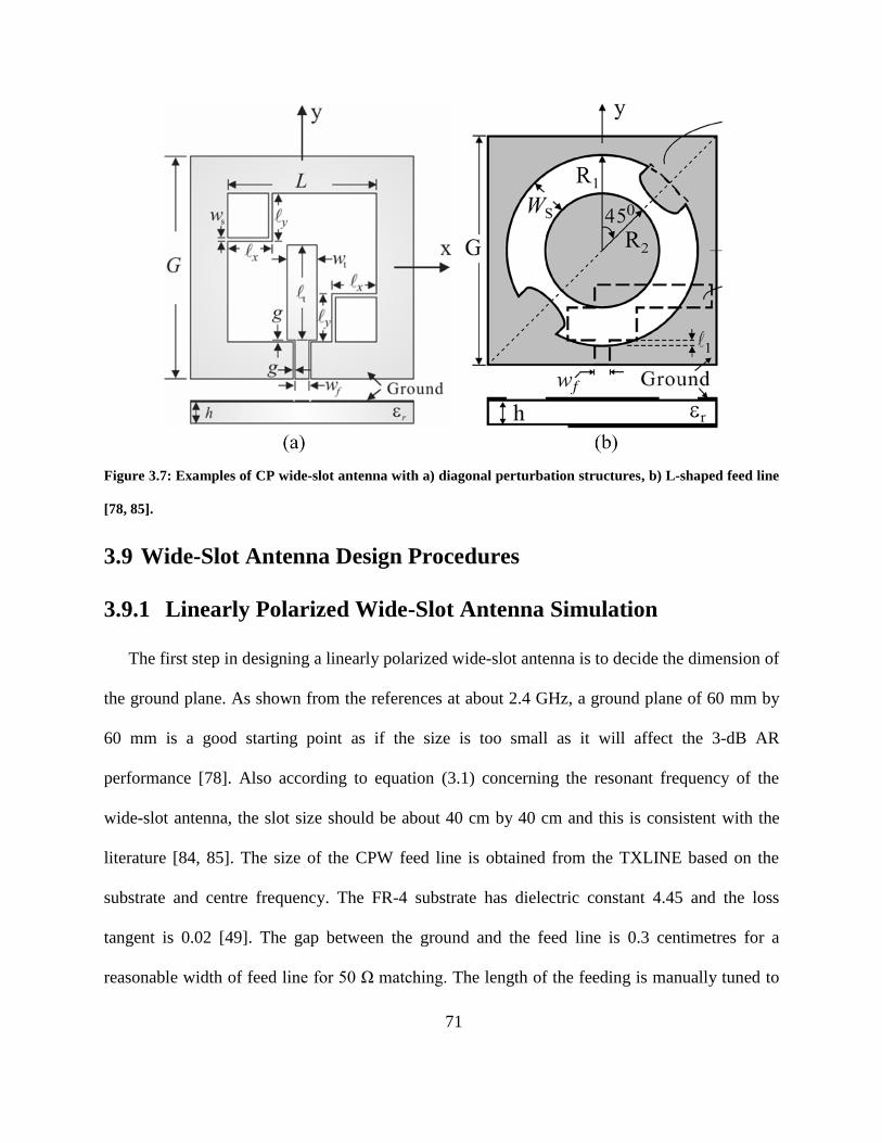
71
Figure 3.7: Examples of CP wide-slot antenna with a) diagonal perturbation structures, b) L-shaped feed line
[78, 85].
3.9 Wide-Slot Antenna Design Procedures
3.9.1 Linearly Polarized Wide-Slot Antenna Simulation
The first step in designing a linearly polarized wide-slot antenna is to decide the dimension of
the ground plane. As shown from the references at about 2.4 GHz, a ground plane of 60 mm by
60 mm is a good starting point as if the size is too small as it will affect the 3-dB AR
performance [78]. Also according to equation (3.1) concerning the resonant frequency of the
wide-slot antenna, the slot size should be about 40 cm by 40 cm and this is consistent with the
literature [84, 85]. The size of the CPW feed line is obtained from the TXLINE based on the
substrate and centre frequency. The FR-4 substrate has dielectric constant 4.45 and the loss
tangent is 0.02 [49]. The gap between the ground and the feed line is 0.3 centimetres for a
reasonable width of feed line for 50 Ω matching. The length of the feeding is manually tuned to

72
the specific frequency. The final dimension of the antenna is shown in Figure 3.8. In the
simulation, differential ports are used as the ground is on the same metal layer as the input. Ports
„-1‟ are connected the ground and port „1‟ is connected to the feed line and therefore the
simulator will understand the reference ground is the outer metal surrounding the slot.
Figure 3.8: Dimension in mm of a linear polarized wide-slot antenna on a 16 mm FR-4 substrate.
The initial result of a linear polarized slot antenna is shown in Figure 3.9 and a standard patch
antenna performance is also shown for comparison. As shown in the figure, the -10-dB
impedance bandwidth is 29% and it is significantly wider than 1.5% of the patch antenna shown
in the same graph. This advantage is essential because it implies that it has a high tolerance for
manufacturing variations and this is especially important for the flexible textile used in the next
chapter. Moreover, the wide band characteristic makes it suitable for on-body power receiving
textile antenna as the bandwidth is significantly degraded due to the proximity of the human
body. Although the wide bandwidth may susceptible to interference, this is not the problem for
the application of power harvesting. The gain of the patch antenna is higher due to the fact it

73
only radiates into +z direction whilst the wide slot antenna radiates into both +z and –z directions
as shown in Figure 3.10.
Figure 3.9: S11 parameters and gains of the wide-slot antenna and the patch antenna.
Now the simple linearly polarized wide-slot antenna has been simulated and it resonates at
the specific targeted frequency range, a circularly polarized wide-slot will be designed next
based on this simple antenna topology.
2000 2200 2400 2600 2800 3000
Frequency (MHz)
-20
-15
-10
-5
0
5
10
Gai
n (
dB
i)
-30
-25
-20
-15
-10
-5
0
S1
1 (
dB
)
Linear slot antenna
Patch Antenna
Linear slot antenna
Patch Antenna

74
Figure 3.10: Radiation pattern for a wide-slot antenna and a patch antenna. a) φ = 0, b) φ = 90°.
0-10-2
0
-30
-40
-50
-60
-70
-80
-90
-100
-110
-120
-130
-140
-150
-160
-17
0 18
0
17
0
160
150
140
130
120
110
100
90
80
70
60
50
40
30
201
0
(a)Mag Max
10 dB
Mag Min
-40 dB
10 dB
Per Div
Linear slot antenna
Patch Antenna
0-10-2
0
-30
-40
-50
-60
-70
-80
-90
-100
-110
-120
-130
-140
-150
-160
-170 1
80
170
160
150
140
130
120
110
100
90
80
70
60
50
40
30
201
0
(b)Mag Max
10 dB
Mag Min
-40 dB
10 dB
Per Div
Linear slot antenna
Patch Antenna

75
3.9.2 Circularly Polarized Wide-Slot Antenna Simulation
As discussed earlier, producing circular polarization on a wide-slot antenna is commonly
done using an L-shaped feed line for a wide bandwidth 3-dB AR bandwidth. The diagonal
perturbation structure inside the slot can be added to further enhance the performance [78].
Therefore, the first attempt is to modify the feed line of the linear polarized wide-slot to L-
shaped as shown in Figure 3.11. The feed line has similar width as the linear polarized wide-slot
antenna, but it is bent at 90° to create the necessary phase delay between the x and y components
of the electric fields as suggested earlier. The exact ratio between the length of the horizontal and
vertical sections is manually tuned and it is easier to start at the centre of the slot and move
around to get the best 3-dB AR ratio.
Figure 3.11: Simple L-shaped feed circularly-polarized wide-slot antenna in mm.
As shown in the Figure 3.12b, for such simple antenna geometry it can offer very wide 3-dB
AR bandwidth with very little effort. The 3-dB bandwidth is 50% from 2.26 GHz to 3.78 GHz

76
and is much wider than the 2.45 GHz ISM band. Note that the gap between the feed line and the
ground has a significant effect on impedance matching at the lower frequency range as it
provides strong coupling to the ground [90, 91]. However, it cannot be smaller than 5 mm as it
will be very difficult to hand-make on a conductive textile as will be shown in the next chapter.
Figure 3.12: Characteristic of the simple L-shaped feed wide-slot antenna a) S11, b) 3-dB AR.
However, as shown in Figure 3.12a the -10-dB impedance bandwidth is not sufficient to
cover the whole 3-dB AR band and the ISM band. This is mainly due to the low input impedance
and this can be improved by increasing the width of the feed line as suggested [78]. The tapering
technique for better input impedance matching has been commonly used in wideband antenna
designs [77, 92]. It is found that 2-level tapering of the feed line will give sufficient impedance
matching across the ISM band and this finding is consistent with the literature [78, 92]. There is

77
an additional tuning stub on the vertical section of the feed line to further improve impedance
bandwidth towards the lower frequency end. The stub will also change the current flow in the
feed and so it will affect the generation of circular polarization. The exact dimension of the feed
is given in the Figure 3.13 and the dimension of the ground is kept the same, 60 mm by 60 mm,
as before. The dimension of the feed line has to be carefully tuned as it affects both the
impedance and 3-dB AR bandwidths at the same time.
Figure 3.13: Dimensions of the tapered L-shaped feed wide-slot antenna in mm.
As shown in Figure 3.14, the impedance bandwidth is 66% from 2.1 GHz to 4.1 GHz and it is
significantly wider than the one from the original simple L-shaped wide-slot antenna and the
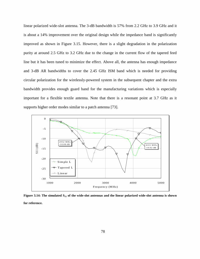
78
linear polarized wide-slot antenna. The 3-dB bandwidth is 57% from 2.2 GHz to 3.9 GHz and it
is about a 14% improvement over the original design while the impedance band is significantly
improved as shown in Figure 3.15. However, there is a slight degradation in the polarization
purity at around 2.5 GHz to 3.2 GHz due to the change in the current flow of the tapered feed
line but it has been tuned to minimize the effect. Above all, the antenna has enough impedance
and 3-dB AR bandwidths to cover the 2.45 GHz ISM band which is needed for providing
circular polarization for the wirelessly-powered system in the subsequent chapter and the extra
bandwidth provides enough guard band for the manufacturing variations which is especially
important for a flexible textile antenna. Note that there is a resonant point at 3.7 GHz as it
supports higher order modes similar to a patch antenna [73].
Figure 3.14: The simulated S11 of the wide-slot antennas and the linear polarized wide-slot antenna is shown
for reference.
1000 2000 3000 4000 5000
Frequency (M Hz)
-30
-25
-20
-15
-10
-5
0
S1
1 (
dB
)
41 0 1 M H z
-1 0 .0 2 dB
2 0 52 M H z
-1 0.0 8 d B
Sim ple L
Tapered L
Linear

79
Figure 3.15: The simulated axial ratios for the wide-slot antennas.
3.9.3 Circular Polarization Mechanism
The basic idea of generating circular polarization using the L-shaped feed has been briefly
described in an earlier section. The common way to verify this is to study the magnetic current
flow quantitatively in a simulator [93]. As shown in Figure 3.16, the surface current is simulated
using CST at 2.4 GHz and the current distribution is changing with the time. The majority of the
current is going upward in the +y direction at 0° phase although there is a mixture of currents
going in the different directions. At 90° phase, the majority of the current goes to the +x
direction. At 180° and 270° phases, the current are going in the opposite directions as shown for
0° and 90° phases, respectively. Therefore, the current is turning in a clockwise direction and so
this is left-handed CP as expected.
1000 2000 3000 4000 5000
Frequency (M Hz)
0
1
2
3
4
5
6
7
8
9
10
AR
(d
B)
3 9 26 M H z
3 .01 dB
2 1 73 M H z
2 .99 dB
T ap ered L
S im p le L
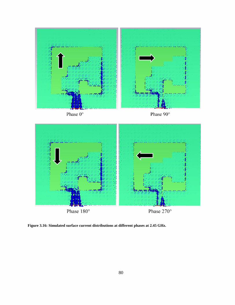
80
Figure 3.16: Simulated surface current distributions at different phases at 2.45 GHz.

81
3.9.4 Circular Polarization Distribution
Although the wide-slot antenna can offer wide 3-dB AR bandwidth in a simple geometry, the
conical angle of the 3-dB AR becomes narrower as the frequency increases. This behaviour is
visualized using CST 3D far-field simulator as shown in Figure 3.17. At 2.45 GHz, the AR
distribution is fairly flat and smooth away from the centre covering a lot of area of the antenna
surface at the far field. It implies that the circular polarization purity can be maintained at wider
angles from the centre and more importantly the LHCP gain is not degraded significantly.
Figure 3.17: AR distribution of the wide-slot antenna at 2.45 GHz.
However, at 3.5 GHz the AR distribution has a lot of spikes around the centre and the AR
rapidly increases even slightly away from the centre as shown in Figure 3.18. This limits the
usefulness of the antenna in the high frequency range as the LCHP gain will decrease more
steeply away from the centre of the antenna in the far field. This problem becomes more
apparent during AR measurement in a later section.

82
Figure 3.18: AR distribution of the wide-slot antenna at 3.5 GHz.
3.9.5 Simulated Radiation Patterns and Gain
The simulated radiation patterns for the wide-slot antenna at 2.45 GHz are shown in Figure
3.19. It is noted that it produces LHCP in +z direction and RHCP in –z direction which is
consistent with the surface current distribution analysis as shown before. It has a good circular
polarization purity at the centre as it has good isolation between the LHCP and the RHCP in +z
direction which is consistent with the 3-dB AR plot. The maximum gain is 3.3 dBic at φ = 10°
and ө = 10° and the gain at centre is 3.1 dBic which is only slightly off from the maximum.
Since the antenna radiates in both +z and –z directions, one suggestion is by adding a
reflector at the back the antenna, the gain can be amplified due to the reflection of the –z
direction radiation [36, 78].
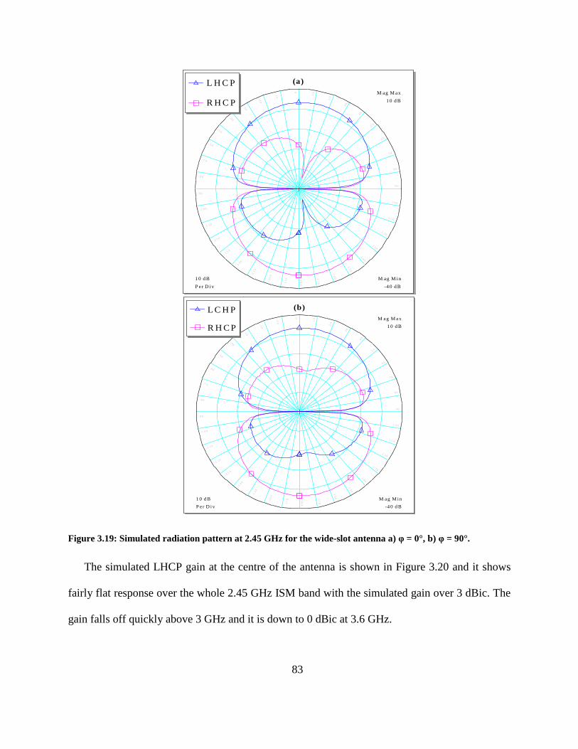
83
Figure 3.19: Simulated radiation pattern at 2.45 GHz for the wide-slot antenna a) φ = 0°, b) φ = 90°.
The simulated LHCP gain at the centre of the antenna is shown in Figure 3.20 and it shows
fairly flat response over the whole 2.45 GHz ISM band with the simulated gain over 3 dBic. The
gain falls off quickly above 3 GHz and it is down to 0 dBic at 3.6 GHz.
0-1
0
-2
0
- 30
- 40
- 5 0
- 6 0
-7 0
- 8 0
- 9 0
-1 0 0
-1 1 0
-12 0
- 1 30
-14
0
-15
0
-1
60
-1
70 1
80
17
0
16
0
15
0
14
0
13 0
1 2 0
1 1 0
1 0 0
9 0
8 0
7 0
6 0
50
40
30
20
10
(a)
M ag M ax
1 0 d B
M ag M in
-4 0 d B
1 0 d B
P er D iv
L H C P
R H C P
0-1
0
-2
0
- 30
- 40
- 5 0
- 6 0
-7 0
- 8 0
- 9 0
-1 0 0
-1 1 0
-12 0
- 1 30
-140
-15
0
-1
60
-1
70 1
80
17
0
16
0
15
0
140
13 0
1 2 0
1 1 0
1 0 0
9 0
8 0
7 0
6 0
50
40
30
20
10
(b)
M ag M ax
1 0 d B
M ag M in
-4 0 d B
1 0 d B
P er D iv
L C H P
R H C P

84
Figure 3.20: Simulated LHCP gain at the centre of the CP wide-slot antenna.
3.10 Experimental Results for the CP Wide-slot Antenna
3.10.1 Measurement Methodology
The measurements are done using a calibrated horn antenna ETS-3115, which has a wide
enough bandwidth to cover the frequency range of interest [94]. Note that the gain of the
calibrated antenna varies slightly over the frequency range, and therefore compensation must be
carried out for the gain measurement of the CP wide-slot antenna. LHCP and RHCP helix
antennas are built to measure the radiation patterns for the wide-slot antenna and the dimension
of the helix antennas are determined using a simple formula [65]. The gains for the helix
antennas are determined using the calibrated horn antenna ETS-3115. The gain measurement for
the wide-slot antenna is measured using the horn antenna in the vertical and horizontal positions
because a linear horn antenna can only pick up half of the radiation from a CP antenna due to
polarization mismatch. Therefore, the gain of a CP antenna is the total sum of the measured gain
1000 2000 3000 4000 5000
Frequency (M Hz)
-15
-10
-5
0
5
Gai
n (
dB
ic)

85
from both horizontal and vertical positions [65]. The measurement of the axial ratio is done by
turning the linear polarized horn antenna to different degrees to obtain the maximum and
minimum gains and the difference between the two is the corresponding axial ratio of the
antenna under test [56, 65]. The horn antenna is the best candidate due to its purity of linear
polarization and stable radiation pattern across a wide frequency range. All measurements are
carried out with an Agilent E8361A PNA inside an anechoic chamber to minimize noise from
the environment and reflections.
The tapered-L CPW-fed CP wide-slot antenna is manufactured in-house using the standard
etching process which is the same as for making of the RF rectifier presented in the previous
chapter and the final design is shown in Figure 3.21.
Figure 3.21: The CP wide-slot antenna on the FR-4.
3.10.2 Experimental Results
The measured S11 of the CP wide-slot antenna is shown in Figure 3.22 and note that the
simulated and measured results are closely matched. At the low frequency end, there is less than
0.1 GHz difference between the 2 results and at the high frequency end they are almost exactly
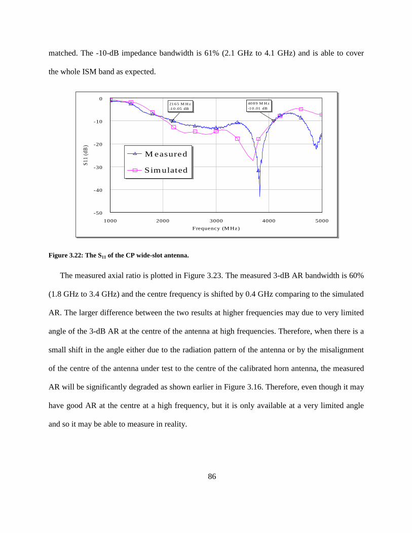
86
matched. The -10-dB impedance bandwidth is 61% (2.1 GHz to 4.1 GHz) and is able to cover
the whole ISM band as expected.
Figure 3.22: The S11 of the CP wide-slot antenna.
The measured axial ratio is plotted in Figure 3.23. The measured 3-dB AR bandwidth is 60%
(1.8 GHz to 3.4 GHz) and the centre frequency is shifted by 0.4 GHz comparing to the simulated
AR. The larger difference between the two results at higher frequencies may due to very limited
angle of the 3-dB AR at the centre of the antenna at high frequencies. Therefore, when there is a
small shift in the angle either due to the radiation pattern of the antenna or by the misalignment
of the centre of the antenna under test to the centre of the calibrated horn antenna, the measured
AR will be significantly degraded as shown earlier in Figure 3.16. Therefore, even though it may
have good AR at the centre at a high frequency, but it is only available at a very limited angle
and so it may be able to measure in reality.
1000 2000 3000 4000 5000
Frequency (M Hz)
-50
-40
-30
-20
-10
0
S1
1 (
dB
)
40 8 9 M H z
-1 0 .01 dB
21 6 5 M H z
-1 0 .05 dB
M easured
Sim ulated

87
Figure 3.23: The measured axial ratio over frequency of the CP wide-slot antenna.
The measured radiation patterns at 2.45 GHz are shown in Figure 3.24. The measured pattern
is closely matched to the simulated pattern shown in Figure 3.19. With LHCP radiation in +z
direction, it radiates at RHCP at the –z direction as expected. The maximum gain is 3.1 dBic at φ
= 10° and ө = 10° which is closely matched to what was predicted in the simulation.
1000 2000 3000 4000 5000
Frequency (M H z)
0
1
2
3
4
5
6
7
8
9
10
AR
(d
B)
3 4 45 M H z
3 .00 7
18 5 2 M H z
3 .0 0 9
M ea sured
Sim u la ted
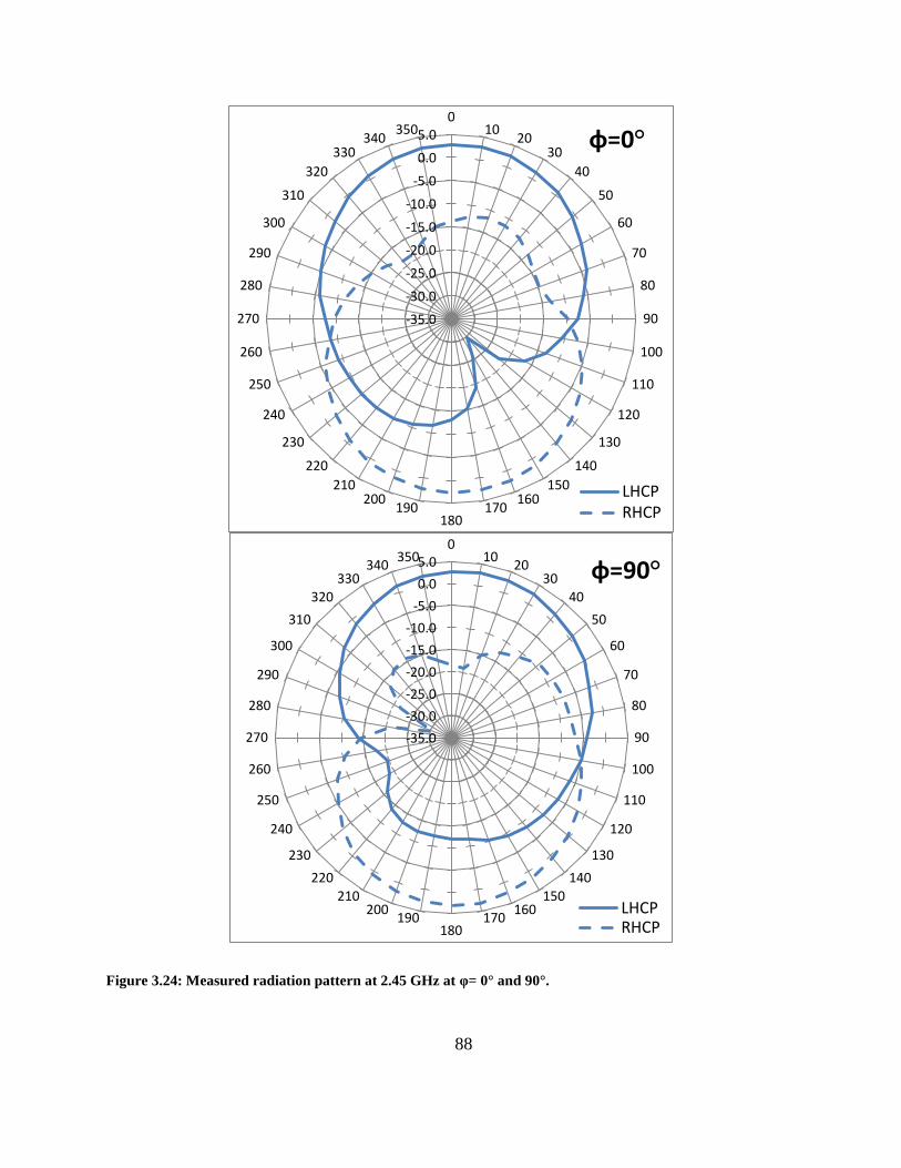
88
Figure 3.24: Measured radiation pattern at 2.45 GHz at φ= 0° and 90°.
-35.0
-30.0
-25.0
-20.0
-15.0
-10.0
-5.0
0.0
5.0 0
10 20
30
40
50
60
70
80
90
100
110
120
130
140
150 160
170 180
190 200
210
220
230
240
250
260
270
280
290
300
310
320
330 340
350 φ=0°
LHCP RHCP
-35.0
-30.0
-25.0
-20.0
-15.0
-10.0
-5.0
0.0
5.0 0
10 20
30 40
50
60
70
80
90
100
110
120
130
140 150
160 170
180 190
200 210
220
230
240
250
260
270
280
290
300
310
320 330
340 350
φ=90°
LHCP RHCP

89
The measured gain for the wide-slot antenna is plotted in Figure 3.25. The LHCP gain at 2.45
GHz is 2.7 dBic and the maximum is 4 dBic at 2.9 GHz. The overall trend of the measured gain
is closely related to the simulated gain as shown.
Figure 3.25: Measured LHCP gain of the wide-slot antenna.
The performance of this wide-slot antenna is summarized in Table 3-1: Performance
comparisons of different antenna designs.. The designs from the other references with the similar
physical area are also included in this table for comparison. The tapered-L feed wide-slot
antenna performs significantly better than those with only simple straightened feed line in terms
of 3-dB AR bandwidth. This work has a comparable 3-dB bandwidth to the one with L-shaped
feed annular-ring wide slot antenna that requires extra metal layer for the microstrip feed line
[78]. As the results suggest the two layer design may offer a more compact design in [78]
because the feed is not constraint by the slot dimension. The only drawback of this work is that
-12.0
-10.0
-8.0
-6.0
-4.0
-2.0
0.0
2.0
4.0
1 1.5 2 2.5 3 3.5 4
Gai
n (
dB
ic)
Frequency (GHz)
Measured Simulated
90
the -10-dB impedance bandwidth is not able to cover the whole 3-dB AR bandwidth even though
the whole 2.45 GHz ISM band is fully covered.
Antenna Area
mm x
mm
Impedance
Bandwidth
3-dB AR
Bandwidth
This work 60x60 61%, 2.1-4.1 GHz 60%, 1.8-3.4 GHz
[76] 70x70 39.6%, 1.6-2.5 GHz 12.4%, 1.8-2.1 GHz
[85] 60x60 52%, 1.6-3.1 GHz 28.8%, 2.3-3.0 GHz
[84] 60x60 51.4%, 2.0-3.4 GHz 48.8%, 2.1-3.4 GHz
[78] 45x45 79%, 2.0-4.7 GHz 56.2%, 2.1-3.7 GHz
Table 3-1: Performance comparisons of different antenna designs.
3.11 Conclusion
The characteristics of the tapered-L feed wide-slot antenna has been investigated in this
chapter and it has shown significant advantages in terms of impedance and AR bandwidth over a
standard CP patch antenna while the geometry is still relatively simple. In the next chapter, this
wide-slot antenna geometry will be implemented on a conductive textile for an on-body power
transmission application.

91
Chapter 4: Textile Antenna Design
4.1 Introduction
Recently there has been growing use of textile antennas for body-centric applications such as
healthcare, GPS and fire fighter personal communications [7, 29, 32, 33, 35, 67, 95-98]. A textile
antenna is chosen for such applications due to its light-weight and easy integration into clothing.
Designing a wide band CP wide-slot antenna on FR-4 has been successfully demonstrated in
Chapter 3. Although the antenna design in Chapter 3 has a very wide bandwidth, that antenna
design still may be too complicated to be implemented on a flexible textile. The complex
geometry is hard to be maintained when the antenna is under physical stress on a body. For
body-worn antenna application, a simpler and more robust antenna geometry is needed to be
easily hand-made on a flexible conductive material. In order to translate the antenna geometry to
a conductive textile, this chapter firstly starts with off-body simulation of the conductive textile
with felt as the flexible substrate for the wide-slot antenna design. Then, the simulation model
with body tissues is considered and the antenna is optimized in that environment. Once the
simulation is complete, the antenna is built on a self-adhesive conductive textile with felt as the
substrate. Finally, the antenna characteristics are measured under different conditions such as
substrate thickness and bending.
4.2 Recent Developments of Textile Antenna
Patch or dipole antennas are the most common topologies for the textile antennas and there
are some other special types in the forms of a belt, a zipper and a button as shown in Figure 4.1
[98-100]. A textile patch antenna with a ground plane is preferred because it can minimize the
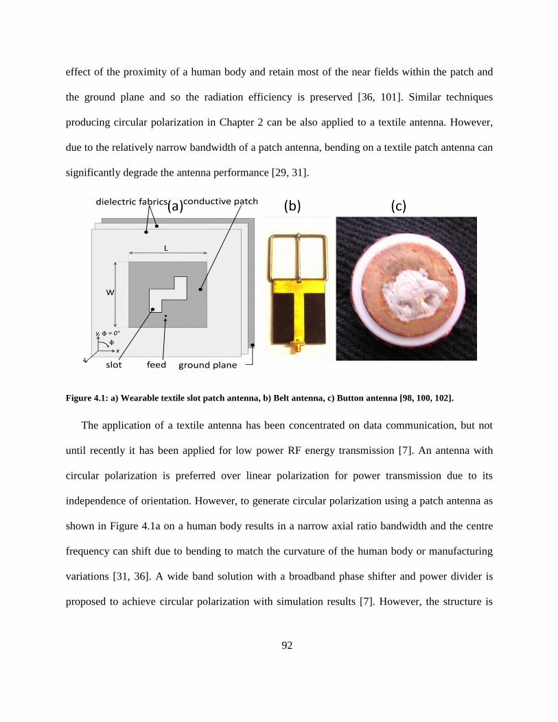
92
effect of the proximity of a human body and retain most of the near fields within the patch and
the ground plane and so the radiation efficiency is preserved [36, 101]. Similar techniques
producing circular polarization in Chapter 2 can be also applied to a textile antenna. However,
due to the relatively narrow bandwidth of a patch antenna, bending on a textile patch antenna can
significantly degrade the antenna performance [29, 31].
Figure 4.1: a) Wearable textile slot patch antenna, b) Belt antenna, c) Button antenna [98, 100, 102].
The application of a textile antenna has been concentrated on data communication, but not
until recently it has been applied for low power RF energy transmission [7]. An antenna with
circular polarization is preferred over linear polarization for power transmission due to its
independence of orientation. However, to generate circular polarization using a patch antenna as
shown in Figure 4.1a on a human body results in a narrow axial ratio bandwidth and the centre
frequency can shift due to bending to match the curvature of the human body or manufacturing
variations [31, 36]. A wide band solution with a broadband phase shifter and power divider is
proposed to achieve circular polarization with simulation results [7]. However, the structure is

93
complicated to manufacture as shown in Figure 4.2 and there is no measured result to prove its
power efficiency.
Figure 4.2: Wearable multi-frequency RF energy harvesting textile antenna [7].
In Chapter 3, a high performance wide-slot circularly polarized antenna has been proposed. A
CPW-fed antenna features wide impedance and axial ratio bandwidths that are essential to body-
worn textile antenna applications as it has a higher tolerance to different conditions on a human
body. Also it only consists of a single layer of metalized textile without a separate ground plane.
Therefore, a cost effective body-worn textile antenna can be designed based on a wide-slot
antenna topology. However, due to the missing ground plane, the influence of the human body
on the antenna‟s near field has to be carefully simulated in MWO to ensure the effectiveness of
operation. Also the antenna structure has to be simple and robust enough for bending on a human
arm and is able to operate at various distances from a human body.

94
4.3 Textile Antenna Simulation
Before designing a textile antenna for efficient power transmission on-body, the material has
to be chosen and the dielectric constant of the substrate has to be determined. Then the wide-slot
antenna design from Chapter 3 can be optimized in the simulator within the proximity of a
human body.
4.3.1 Textile Materials
A planar textile antenna consists of 2 layers, the top layer is conductive and the bottom layer
is the substrate. Both materials have to be highly flexible but also rigid enough to conform to any
surface of a human body. A Flectron™ self-adhesive EMI shielding sheet has been chosen for
this purpose due to its flexibility and high conductivity ≤0.070 Ω/²) at very low cost. It is made
of a thin metal coating of nickel on non-woven fabrics and it can be easily cut without a special
tool [103]. A common 1 mm-thick 100% acrylic self-adhesive felt is chosen as the substrate for
the antenna due to its flexibility and easy stacking for different thickness. The dielectric constant
and loss tangent are determined as 1.5 and 0.02, respectively, by matching the experimental and
simulation results of a simple patch antenna at a specific frequency [104]. Since the loss tangent
of the felt substrate is similar to FR-4, therefore the efficiency of the textile antenna is similar to
a design with FR-4 substrate.
4.3.2 Textile Wide-slot Antenna Simulation
The wide-slot antenna with wide impedance and axial ratio bandwidths has been designed in
Chapter 3. However, the same design on FR-4 is needed to scale manually according to equation
(3.1) in Chapter 3 due to the change in the dielectric constant of the substrate. Also note that the
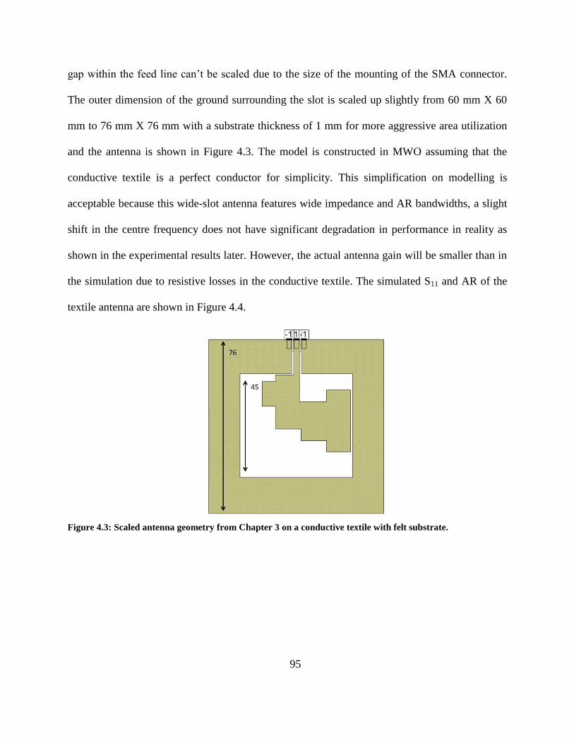
95
gap within the feed line can‟t be scaled due to the size of the mounting of the SMA connector.
The outer dimension of the ground surrounding the slot is scaled up slightly from 60 mm X 60
mm to 76 mm X 76 mm with a substrate thickness of 1 mm for more aggressive area utilization
and the antenna is shown in Figure 4.3. The model is constructed in MWO assuming that the
conductive textile is a perfect conductor for simplicity. This simplification on modelling is
acceptable because this wide-slot antenna features wide impedance and AR bandwidths, a slight
shift in the centre frequency does not have significant degradation in performance in reality as
shown in the experimental results later. However, the actual antenna gain will be smaller than in
the simulation due to resistive losses in the conductive textile. The simulated S11 and AR of the
textile antenna are shown in Figure 4.4.
Figure 4.3: Scaled antenna geometry from Chapter 3 on a conductive textile with felt substrate.

96
Figure 4.4: The simulated characteristics of the textile antenna: a) S11, b) AR.
The simulated S11 of the textile antenna is very similar to the one shown in Figure 3.14 as
expected and the -10-dB impedance bandwidth is 1.6 GHz (2.1-3.8 GHz). The AR bandwidth is
wider than is shown in Figure 3.15 but it is very close to 3-dB at 3.3 GHz and the 3-dB AR
bandwidth is 2.3 GHz (2.1-4.4 GHz). As shown in this simulation, the textile antenna performs
in a similar way as the wide-slot antenna on FR-4 after size scaling. However, the simulation of a
textile antenna on-body is necessary because the coupling of the human body can significantly
affect the antenna performance [101].
4.3.3 Textile Wide-Slot Antenna On-Body Simulation
As the textile antenna is to be worn on a human body, due to the dielectric constant of a
human body, the centre frequency of the textile is shifted to a higher frequency according to
equation 3.1 in Chapter 3 [101]. The dielectric constants of human tissue from 10 Hz to 100 GHz

97
have been studied in detail in the literature [105-108]. Therefore, the simulation model in MWO
will be based on these dielectric constants and are listed in Table 4-1 [108].
Tissue Conductivity Relative Loss Penetration
[S/m] permittivity tangent depth (m)
Skin 1.46 38 0.28 0.023
Fat 0.11 5.28 0.15 0.117
Bone 0.81 18.5 0.32 0.029
Muscle 1.73 52.7 0.017 0.022
Air 0 1 0 N/A
Table 4-1: Dielectric constants and penetration depth for human tissues at 2.45 GHz [108].
The thickness of each human tissue is based on the cross section of a human body from the
Visible Human Project as shown in Figure 4.5 [109]. This cross section provides a good
estimation for the tissue thickness of a human arm and body. Note that different people and
different parts of a body will have different distributions of tissues as the model used in Figure
4.6. As shown in the model, skin, fat, muscle and bone are modelled with estimated thickness
and the antenna is on top of the skin. The thickness of each layer is adjusted according to the
observation from Figure 4.5. Note that only one side of a human body is specified because
microwave at 2.45 GHz can‟t go deep inside a human body according to the penetration depth in
Table 4.1. The total thickness of the human tissue model already exceeds the penetration depth.
Therefore, the textile antenna being under the air and on top of the skin, fat, muscle and bone in
the model is sufficient for simulation accuracy.

98
Figure 4.5: Cross section of a human body on a 1 cm by 1 cm grid [109].
Figure 4.6: Human model with different layers of tissues in simulation.

99
The simulated results of the textile antenna with the human model are shown in Figure 4.7.
As predicted by equation (3.1), the centre frequency is inversely proportional to the square root
of the dielectric constant. Since the human body has much higher dielectric constant than air,
therefore the centre frequency of both S11 and AR of the textile antenna on-body are shifted to a
lower frequency. The centre frequency is shifted significantly due to a missing ground plane
when comparing to a patch antenna design with a ground plane. However, not only the
manufacturing cost is lower without an extra layer of conductive material as a ground plane, but
also a human body can serve as a reflector that will increase the gain of the antenna as shown
later in this chapter. Based on this simulation, the textile antenna has to be redesigned to shift the
frequency back to the 2.45 GHz ISM band for the intended application.
Figure 4.7: Simulated characteristics of the textile antenna close to human body: a) S11, b) AR.

100
Another observation is that the distance between the antenna and the body has a significant
effect on the antenna gain as shown in Figure 4.8. When the substrate thickness is 1 mm, the gain
at 2.45 GHz is only -8.6 dBic. It is because the near field of the antenna is coupled to the human
body and the energy loss is significant [32, 101]. As the substrate thickness is increased, the
antenna gain is increased accordingly up to about 5 dBic when the thickness is at 20 mm. There
is no significant increase in gain with the substrate thickness greater than 20 mm; however, with
the felt thickness being 20 mm on a human arm, it may be too bulky to be bent and worn.
Therefore, a 13 mm thick substrate is chosen to be the minimum thickness for future simulation
and optimization, as the further increase in thickness will not offer significant gain. The
thickness will be increased experimentally to obtain better antenna gain for the power
transmission application with proximity to a human body.
Figure 4.8: Antenna gains with different substrate thicknesses.
1500 2500 3500 4500
Frequency (M Hz)
-20
-15
-10
-5
0
5
10
RH
CP
Gai
n (
dB
ic)
2 0m m
7m m
1m m
13m m
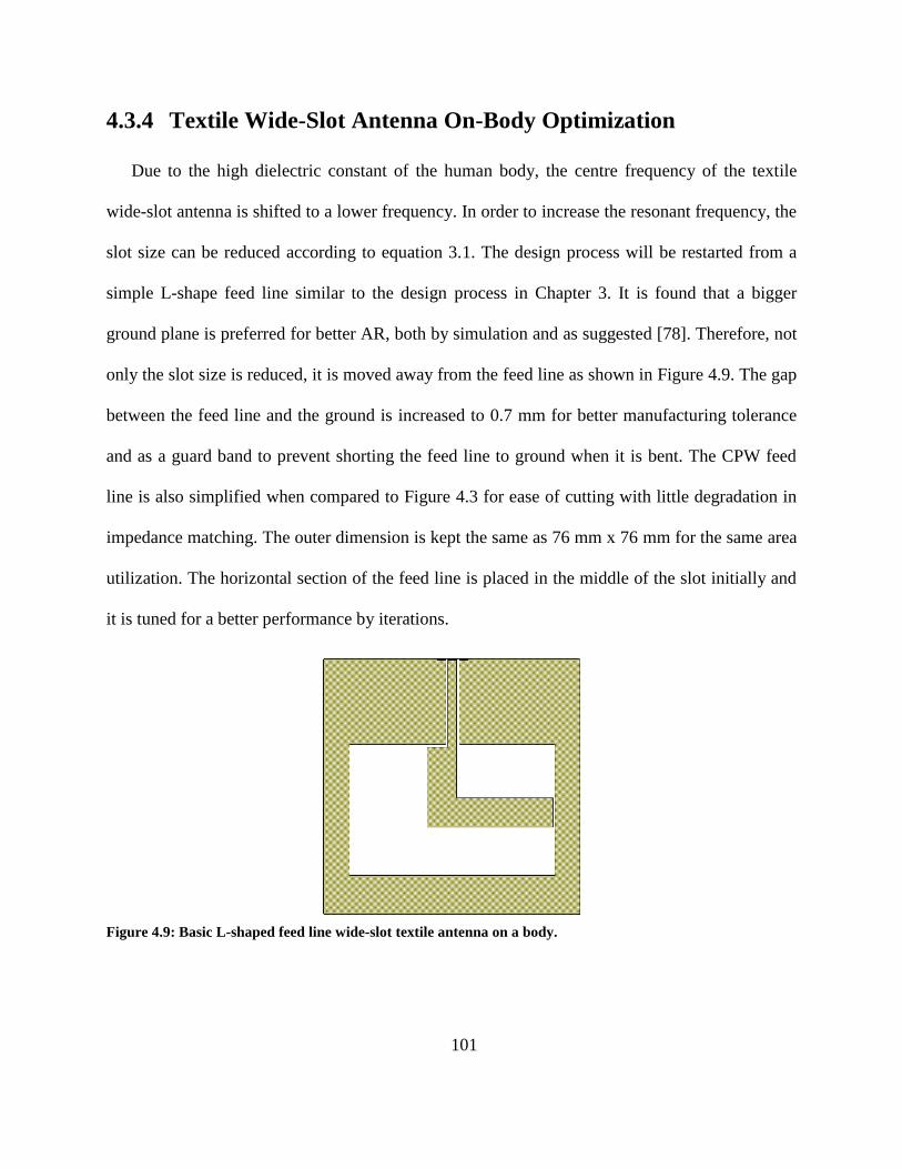
101
4.3.4 Textile Wide-Slot Antenna On-Body Optimization
Due to the high dielectric constant of the human body, the centre frequency of the textile
wide-slot antenna is shifted to a lower frequency. In order to increase the resonant frequency, the
slot size can be reduced according to equation 3.1. The design process will be restarted from a
simple L-shape feed line similar to the design process in Chapter 3. It is found that a bigger
ground plane is preferred for better AR, both by simulation and as suggested [78]. Therefore, not
only the slot size is reduced, it is moved away from the feed line as shown in Figure 4.9. The gap
between the feed line and the ground is increased to 0.7 mm for better manufacturing tolerance
and as a guard band to prevent shorting the feed line to ground when it is bent. The CPW feed
line is also simplified when compared to Figure 4.3 for ease of cutting with little degradation in
impedance matching. The outer dimension is kept the same as 76 mm x 76 mm for the same area
utilization. The horizontal section of the feed line is placed in the middle of the slot initially and
it is tuned for a better performance by iterations.
Figure 4.9: Basic L-shaped feed line wide-slot textile antenna on a body.
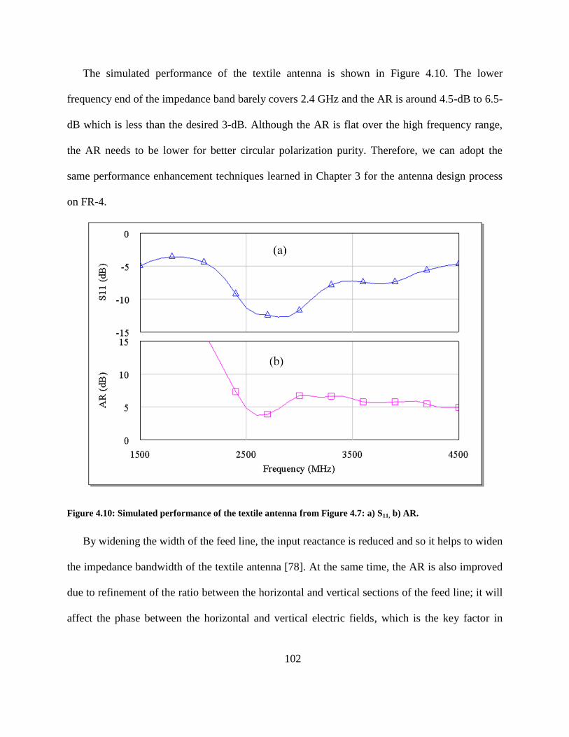
102
The simulated performance of the textile antenna is shown in Figure 4.10. The lower
frequency end of the impedance band barely covers 2.4 GHz and the AR is around 4.5-dB to 6.5-
dB which is less than the desired 3-dB. Although the AR is flat over the high frequency range,
the AR needs to be lower for better circular polarization purity. Therefore, we can adopt the
same performance enhancement techniques learned in Chapter 3 for the antenna design process
on FR-4.
Figure 4.10: Simulated performance of the textile antenna from Figure 4.7: a) S11, b) AR.
By widening the width of the feed line, the input reactance is reduced and so it helps to widen
the impedance bandwidth of the textile antenna [78]. At the same time, the AR is also improved
due to refinement of the ratio between the horizontal and vertical sections of the feed line; it will
affect the phase between the horizontal and vertical electric fields, which is the key factor in
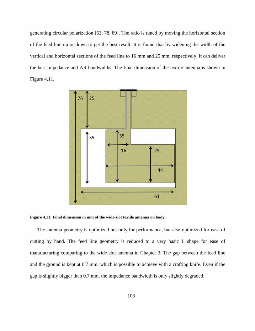
103
generating circular polarization [63, 78, 89]. The ratio is tuned by moving the horizontal section
of the feed line up or down to get the best result. It is found that by widening the width of the
vertical and horizontal sections of the feed line to 16 mm and 25 mm, respectively, it can deliver
the best impedance and AR bandwidths. The final dimension of the textile antenna is shown in
Figure 4.11.
Figure 4.11: Final dimension in mm of the wide-slot textile antenna on body.
The antenna geometry is optimized not only for performance, but also optimized for ease of
cutting by hand. The feed line geometry is reduced to a very basic L shape for ease of
manufacturing comparing to the wide-slot antenna in Chapter 3. The gap between the feed line
and the ground is kept at 0.7 mm, which is possible to achieve with a crafting knife. Even if the
gap is slightly bigger than 0.7 mm, the impedance bandwidth is only slightly degraded.

104
The simulated performance of the wide-slot antenna on body is shown in Figure 4.12. The
impedance bandwidth is 40% (2.1 – 3.1 GHz) and the 3-dB AR bandwidth is 25% (2.2 – 2.8
GHz). The maximum AR bandwidth achieved is degraded compared to the FR-4 counterpart
which may be due to body reflection as suggested [78]. However, the goal for this textile antenna
is to deliver robust power transmission within the proximity of a human body in the 2.45GHz
ISM band and the simulation shows that the whole ISM band is well covered with this textile
antenna.
Figure 4.12: The simulated performance of the textile antenna: a) S11, b) AR.
The radiation patterns of the textile antenna at 2.45 GHz are plotted in Figure 4.13. Both
patterns show very good separation between the RHCP and LHCP, which is consistent with the

105
AR shown in Figure 4.12 earlier. The maximum gain of the pattern is very close to the centre of
the antenna which is desirable for power transmission.
Figure 4.13: The simulated radiation pattern of the textile antenna at 2.45 GHz: a) φ = 0°, b) φ = 90°.
0-10-20
-30
-40
-50
-6 0
- 7 0
- 8 0
- 9 0
- 1 0 0
- 11 0
- 120
-130
-140
-150
-160
-170 1
80
170
160
150
140
130
12 0
1 1 0
1 0 0
9 0
8 0
7 0
6 0
50
40
30
20
10
(a)
M ag Max
1 0 dB
M ag Min
-4 0 dB
10 dB
Per D iv
L H C P
R H C P
0-10-20
-30
-40
-50
-6 0
- 7 0
- 8 0
- 9 0
- 1 0 0
- 11 0
- 120
-130
-140
-150
-160
-170 1
80
170
160
150
140
130
12 0
1 1 0
1 0 0
9 0
8 0
7 0
6 0
50
40
30
20
10
(b)
M ag Max
1 0 dB
M ag Min
-4 0 dB
10 dB
Per D iv
L HC P
RH CP
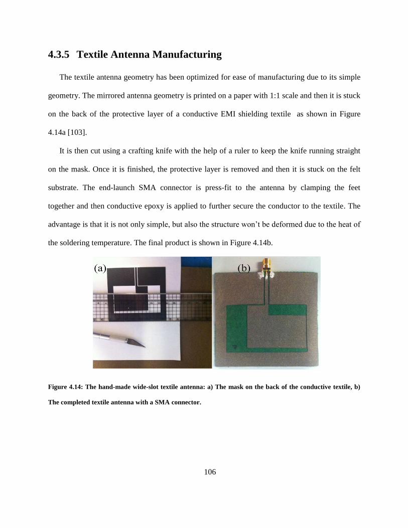
106
4.3.5 Textile Antenna Manufacturing
The textile antenna geometry has been optimized for ease of manufacturing due to its simple
geometry. The mirrored antenna geometry is printed on a paper with 1:1 scale and then it is stuck
on the back of the protective layer of a conductive EMI shielding textile as shown in Figure
4.14a [103].
It is then cut using a crafting knife with the help of a ruler to keep the knife running straight
on the mask. Once it is finished, the protective layer is removed and then it is stuck on the felt
substrate. The end-launch SMA connector is press-fit to the antenna by clamping the feet
together and then conductive epoxy is applied to further secure the conductor to the textile. The
advantage is that it is not only simple, but also the structure won‟t be deformed due to the heat of
the soldering temperature. The final product is shown in Figure 4.14b.
Figure 4.14: The hand-made wide-slot textile antenna: a) The mask on the back of the conductive textile, b)
The completed textile antenna with a SMA connector.
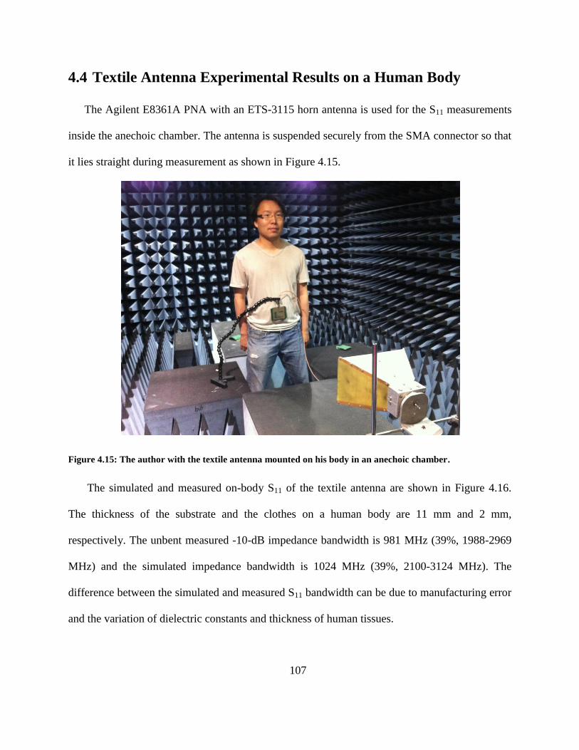
107
4.4 Textile Antenna Experimental Results on a Human Body
The Agilent E8361A PNA with an ETS-3115 horn antenna is used for the S11 measurements
inside the anechoic chamber. The antenna is suspended securely from the SMA connector so that
it lies straight during measurement as shown in Figure 4.15.
Figure 4.15: The author with the textile antenna mounted on his body in an anechoic chamber.
The simulated and measured on-body S11 of the textile antenna are shown in Figure 4.16.
The thickness of the substrate and the clothes on a human body are 11 mm and 2 mm,
respectively. The unbent measured -10-dB impedance bandwidth is 981 MHz (39%, 1988-2969
MHz) and the simulated impedance bandwidth is 1024 MHz (39%, 2100-3124 MHz). The
difference between the simulated and measured S11 bandwidth can be due to manufacturing error
and the variation of dielectric constants and thickness of human tissues.
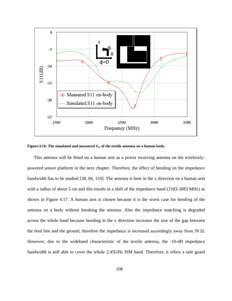
108
Figure 4.16: The simulated and measured S11 of the textile antenna on a human body.
This antenna will be fitted on a human arm as a power receiving antenna on the wirelessly-
powered sensor platform in the next chapter. Therefore, the effect of bending on the impedance
bandwidth has to be studied [38, 66, 110]. The antenna is bent in the x direction on a human arm
with a radius of about 5 cm and this results in a shift of the impedance band (2183-3083 MHz) as
shown in Figure 4.17. A human arm is chosen because it is the worst case for bending of the
antenna on a body without breaking the antenna. Also the impedance matching is degraded
across the whole band because bending in the x direction increases the size of the gap between
the feed line and the ground, therefore the impedance is increased accordingly away from 50 Ω.
However, due to the wideband characteristic of the textile antenna, the -10-dB impedance
bandwidth is still able to cover the whole 2.45GHz ISM band. Therefore, it offers a safe guard

109
band for any shifting in resonant frequency due to bending and variation of dielectric constants
of a human body.
Figure 4.17: The measured bent and unbent S11 of the textile antenna on a human body.
The axial ratio is an indicator of the quality of circular polarization. The simulated and
measured axial ratios at the centre of the textile antenna are shown in Figure 4.18. The simulated
and measured 3-dB axial-ratio bandwidths (ARBW) are 591 MHz (23%, 2237-2828 MHz) and
443 MHz (18%, 2226-2669 MHz), respectively. The small difference may be due to the
curvature of a human body and mismatch in dielectric constant from the model in the simulator.
However, the 3-dB ARBW is still more than enough to cover the whole 2.45GHz ISM band with
good circular polarization purity and is significantly wider than a standard circularly polarized
patch [31, 67, 111]. Bending the textile antenna on a human arm has a small effect on the 3-dB
ARBW (413 MHz) and has shifted the central frequency slightly higher, and hence the wide
impedance and AR bandwidths are still maintained on a human body.
1500 2000 2500 3000 3500
Frequency (M Hz)
-30
-25
-20
-15
-10
-5
0
S1
1 (
dB
)
2183 M Hz
-10.1 dB
M easured Unbent S11
M easured B ent S 11
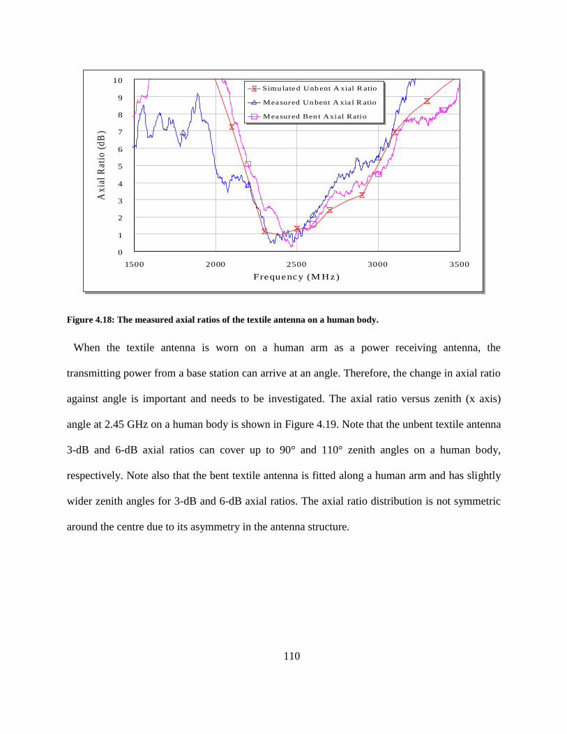
110
Figure 4.18: The measured axial ratios of the textile antenna on a human body.
When the textile antenna is worn on a human arm as a power receiving antenna, the
transmitting power from a base station can arrive at an angle. Therefore, the change in axial ratio
against angle is important and needs to be investigated. The axial ratio versus zenith (x axis)
angle at 2.45 GHz on a human body is shown in Figure 4.19. Note that the unbent textile antenna
3-dB and 6-dB axial ratios can cover up to 90° and 110° zenith angles on a human body,
respectively. Note also that the bent textile antenna is fitted along a human arm and has slightly
wider zenith angles for 3-dB and 6-dB axial ratios. The axial ratio distribution is not symmetric
around the centre due to its asymmetry in the antenna structure.
1500 2000 2500 3000 3500
Frequency (M Hz)
0
1
2
3
4
5
6
7
8
9
10
Ax
ial
Ra
tio
(d
B)
Simu lated Unb ent A xial R atio
Measured Un bent A xia l R atio
Measured Ben t Axial Ratio
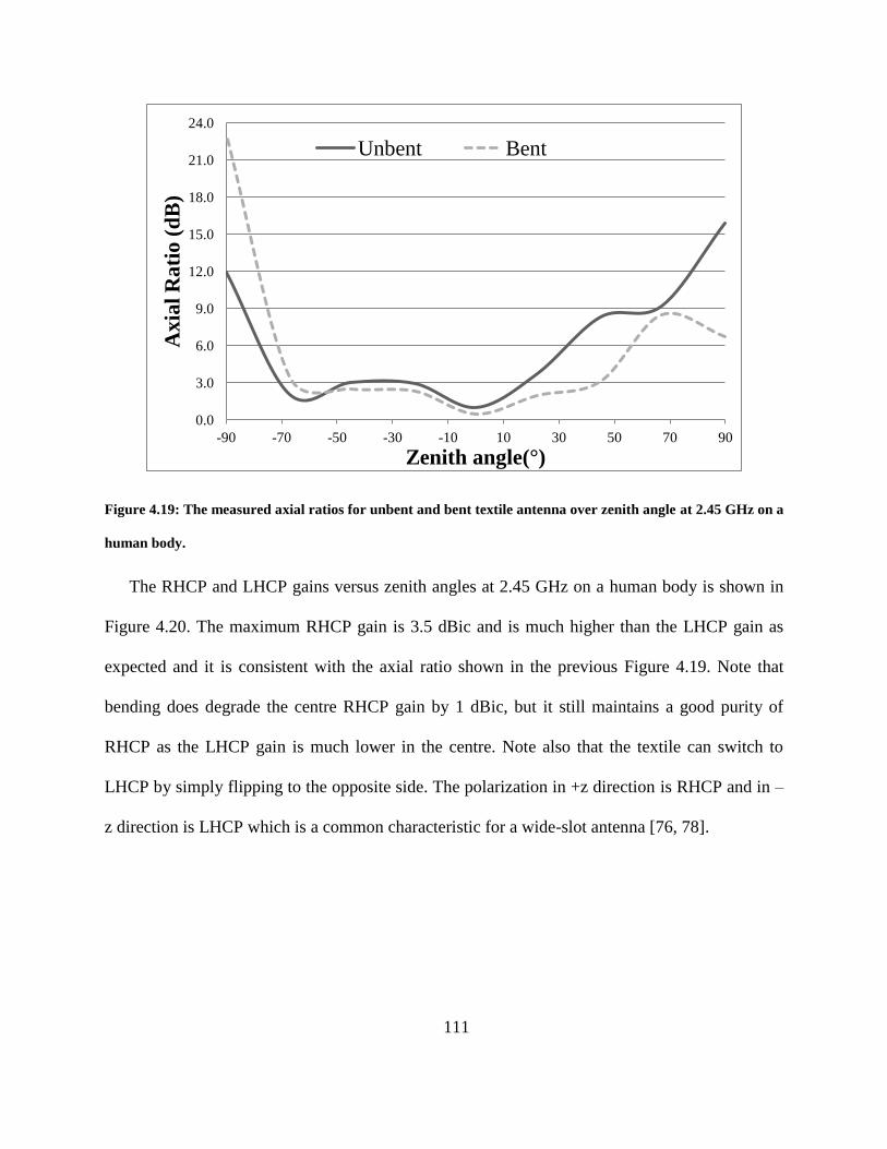
111
Figure 4.19: The measured axial ratios for unbent and bent textile antenna over zenith angle at 2.45 GHz on a
human body.
The RHCP and LHCP gains versus zenith angles at 2.45 GHz on a human body is shown in
Figure 4.20. The maximum RHCP gain is 3.5 dBic and is much higher than the LHCP gain as
expected and it is consistent with the axial ratio shown in the previous Figure 4.19. Note that
bending does degrade the centre RHCP gain by 1 dBic, but it still maintains a good purity of
RHCP as the LHCP gain is much lower in the centre. Note also that the textile can switch to
LHCP by simply flipping to the opposite side. The polarization in +z direction is RHCP and in –
z direction is LHCP which is a common characteristic for a wide-slot antenna [76, 78].
0.0
3.0
6.0
9.0
12.0
15.0
18.0
21.0
24.0
-90 -70 -50 -30 -10 10 30 50 70 90
Axia
l R
ati
o (
dB
)
Zenith angle(°)
Unbent Bent

112
Figure 4.20: The measured gains for unbent and bent textile antennas over zenith angle.
The thickness of the substrate has a significant effect on the textile antenna gain especially as
the ground plane is missing because the near field is coupled and absorbed into the body. As the
distance between the antenna and a body is increased, the body will behave like a reflector to
strengthen the antenna gain as shown in Figure 4.21 [95, 101, 112]. When the minimum distance
between the conductive textile to a human body is at 3 mm (1 mm substrate + 2 mm of clothes),
the gain is weak due to its near field significantly coupled to the human body [36, 101, 112].
However, as the distance increases by inserting the more layers of felt, the gain gradually
increases up to maximum 4.9 dBic at the substrate thickness of 23 mm and the gain goes down
as the resonant frequency is shifted away from 2.45 GHz. It is due to the fact that the human
body serves as a reflector, part of the –z direction LHCP radiation is reflected and it becomes
RHCP in +z direction and so the +z direction RHCP gain is strengthened due to the reflected
-25.0
-20.0
-15.0
-10.0
-5.0
0.0
5.0
-90 -70 -50 -30 -10 10 30 50 70 90
Gain
(d
Bic
)
Zenith angle(°)
Unbent RHCP
Bent RHCP
Unbent LHCP
Bent LHCP
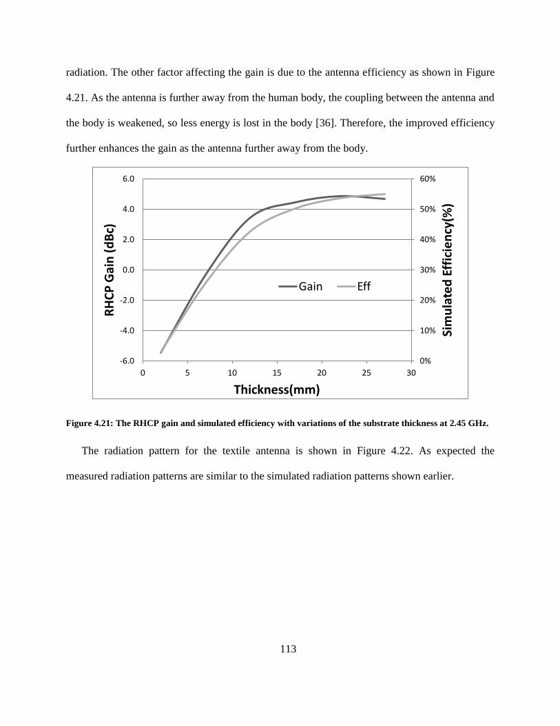
113
radiation. The other factor affecting the gain is due to the antenna efficiency as shown in Figure
4.21. As the antenna is further away from the human body, the coupling between the antenna and
the body is weakened, so less energy is lost in the body [36]. Therefore, the improved efficiency
further enhances the gain as the antenna further away from the body.
Figure 4.21: The RHCP gain and simulated efficiency with variations of the substrate thickness at 2.45 GHz.
The radiation pattern for the textile antenna is shown in Figure 4.22. As expected the
measured radiation patterns are similar to the simulated radiation patterns shown earlier.
0%
10%
20%
30%
40%
50%
60%
-6.0
-4.0
-2.0
0.0
2.0
4.0
6.0
0 5 10 15 20 25 30
Sim
ula
ted
Eff
icie
ncy
(%)
RH
CP
Gai
n (
dB
c)
Thickness(mm)
Gain Eff

114
Figure 4.22: The measured radiation patterns at 2.45GHz with φ = 0°and φ = 90°.
The performance comparisons of this CP textile antenna to the other CP textile antennas are
summarized in Table 4-2. As shown in the table, all the other works are based on patch antenna
-25.0
-20.0
-15.0
-10.0
-5.0
0.0
5.0 0
10 20
30 40
50
60
70
80
90
100
110
120
130
140 150
160 170
180 190
200 210
220
230
240
250
260
270
280
290
300
310
320 330
340 350
φ=0°
LHCP RHCP
-1.1
-25.0
-20.0
-15.0
-10.0
-5.0
0.0
5.0 0
10 20
30 40
50
60
70
80
90
100
110
120
130
140 150
160 170
180 190
200 210
220
230
240
250
260
270
280
290
300
310
320 330
340 350 φ=90°
LHCP
RHCP

115
designs with a ground plane and a thin substrate which have very small impedance and AR
bandwidths as expected from a patch antenna. This work has shown a significant advantage on
manufacturing simplicity and bandwidths over a standard patch design on a human body.
Antenna
Area
mm x mm
Impedance
Bandwidth
3-dB AR
Bandwidth
This work 76x76 39%, 2.0-3.0 GHz 18%, 2.2-2.7 GHz
[67]
50x50
(excluding ground
plane dimension) 9.3%, 2.35-2.58 GHz
2.4%, 2.4-2.46 GHz
(simulated)
[102] 110x110 5.2%, 1.605-1.690 GHz 1.2%, 1.6-1.62 GHz
[31]
65x65
(excluding ground
plane dimension) 1.9%, 1.6-1.68 GHz 1.8%, 1.61-1.63 GHz
Table 4-2: The performance comparisons of CP textile antennas.
4.5 Conclusion
The design of a wideband circularly polarized textile on-body antenna is presented. The design
has shown its flexibility in terms of geometry, material, impedance bandwidth and 3-dB ARBW.
With 39% impedance bandwidth and 18% 3-dB ARBW on a human body, it has a huge guard
band for manufacturing tolerance and variation of dielectric constants of the different human
body. Its structure is simple as it doesn‟t require a ground plane leading to lower cost and
providing single-fed to produce circular polarization.
Now all the fundamental blocks for building a wirelessly-powered sensor platform are ready and
so the complete sensor system will be constructed and discussed in the next chapter.

116
Chapter 5: Application on Wirelessly-Powered Sensor
Platform
5.1 Introduction
From the previous chapters, the knowledge of the fundamental building blocks for a
wirelessly-powered system has been acquired and now a more complicated sensor platform is
ready to be made. The concept of a wirelessly-powered sensor platform has been briefly
described in Chapter 1 and a simple wirelessly-powered system with a microcontroller
controlling a flashing LED has been demonstrated in Chapter 2. In this chapter the technical
detail of a complete wearable wirelessly-powered temperature sensor system will be
demonstrated including C programming of an ultra low power microcontroller. Due to the weak
RF energy received from the rectifier, a charge-pump IC is introduced for the voltage step-up to
improve the power sensitivity of the system. Once all the temperature data is received at the
microcontroller, a low-power RF transmitter is programmed to send the data back to a remote
laptop for data acquisition. Finally, the system with a textile antenna worn on a human arm
demonstrates the longest workable distance with only 50 mW transmitted power from a base
station. This system is able to successfully transmit the temperature data from the transponder to
a remote laptop in an anechoic chamber.
5.2 Wirelessly-Powered Sensor Platform Design
The top-level architecture is shown in Figure 1.1 in Chapter 1. Similar to other wirelessly-
powered systems, weak RF power is received at the antenna and then the rectifier converts the

117
RF power into a DC voltage. The charge-pump IC steps up the voltage to 2.4 V and the energy is
stored in a capacitor to provide stable system power for later use. The µC performs the timing
and control tasks for the sensor and the RF transmitter. It collects the sensor data and converts it
to a 10-bit number using its internal analogue-to-digital converter (ADC). The RF transmitter is
used for sending the data back to a base station.
5.2.1 Rectifier
The detail of designing the rectifier can be found in Chapter 2. The Skyworks SMS-7630 is
chosen over the HMS-2850 for higher sensitivity. It has been found that single diode
configuration is the most power effective for the power harvesting application due to less energy
loss on components and copper traces on a lossy substrate. The schematic for the single diode
rectifier is shown in Figure 2.13 and FR-4 is chosen as the substrate due to its low cost.
5.2.2 Ultra Low-Power Charge-Pump IC
For the low-power RF energy scavenging application, the input level can be below -15 dBm
(0.03 mW) as shown in Chapter 2. Therefore the voltage collected from the microwave rectifier
is substantially below the normal operating voltage for a µC. The standard voltage multiplier can
help to step up the low input voltage to a higher level. However, due to the energy loss in the
substrate and the finite voltage barrier of the diode at microwave frequencies, putting in more
than 3 or 4 stages of the voltage multiplier does not yield a higher voltage as shown in Chapter 2.
Also, the µC draws current even before it is turned on at 1.8 V and so energy is wasted.
Therefore, a solution is needed to provide a low input voltage and energy efficient voltage step-
up.

118
The Seiko S-882Z charge pump IC is capable of stepping up at the extremely low input
voltage of 0.3 V and the block diagram is shown in Figure 5.1 [54]. The S-882Z is turned on
when the input voltage from the rectifier is at minimum of 0.3 V. The step-up voltage is stored in
the external capacitor CCPOUT. Note that the OUT pin is disconnected from the storage capacitor
and so there no leakage current going to the µC. Once the storage capacitor CCPOUT reaches the
threshold voltage 2.4 V, the gate of M1 will be on and the storage capacitor will discharge to the
OUT pin. The function of pin VM is to shut down the IC when the voltage at pin VM is higher
than CCPOUT + 0.1 V. In this application, pin VM is grounded.
Figure 5.1: Block diagram of the Seiko charge-pump IC [54].
5.2.3 Low-Power Microcontroller
In Chapter 2, a simple system with a µC flashing the LED at a regular time interval was
demonstrated. The Microchip PIC12LF1822 is chosen as the µC for the sensor system due to its
improved low-power consumption and easy-to-use programming interface [113]. It is an 8-bit

119
µC with a built-in 10-bit A/D converter with internal voltage references, comparators, timers and
EPPROM operating on a supply voltage as low as 1.8 V with a typical power consumption 110
µW. The other common choice of µC can be TI MSP430F11 [114]. However, it doesn‟t have
internal voltage references and it is a 16-bit µC with a typical power consumption 352 µW that
consumes too much power for the application in this thesis.
The function of this µC is to receive the analogue temperature data from the sensor and then
the data is converted into a 10-bit number. That number is then formatted into packets and sent to
the RF transmitter so that the remote RF receiver will receive that data and display the results on
a laptop. Therefore, the µC has to coordinate all of the data traffic between chipsets with the
correct timing under the restricted power constraint.
The µC is programmed in C under the MPLAB programming environment and the C
compiler is free from HiC [115-117]. The complete program is listed in the Appendix and the
important sections of the program will be briefly discussed here.
After assigning the function of each pin for the µC, the internal analogue-to-digital converter
(ADC) needs to be configured so that it will convert the analogue data from the pin connected
temperature sensor to a 10-bit number compared to a fixed internal 2.0 V voltage reference:
// configure ADC
ADCON1 = 0b01000011; //use internal voltage reference
ADCON0 = 0b00001001; //use the 2nd ADC and turn it on
FVRCON = 0b10000010; //enable fixed 2.048V internal reference

120
Before sending any packets to the RF transmitter, it needs to be configured whenever it is
powered up and the detailed code for configuring the Nordic N2401G is shown in Appendix
[118, 119]:
__delay_ms(1); // wait 1.5 ms for the transmitter to be ready
__delay_us(500);
configure_transmitter();//configure the transmitter
Since the ADC is already configured, now the µC starts the conversion and waits until the
data is acquired:
// sample analogue input
GO_nDONE = 1; // start conversion
while (GO_nDONE) // wait until done
;
Once the ADC operation is done, the data is stored in 2 registers called ADDRESH and
ADRESL. Now the data is aligned and stored in the array called data_array and ready to be sent
to the RF transmitter. The function of transmit_data() is to shift the data serially to the RF
transmitter and signal the transmitter to send the data back to laptop at 2.52 GHz. The completed
code can be found in Appendix:
//10 bits result
data_array[0] = ADRESH;
//Top 8-bit ADC result
data_array[1] = ADRESL;
__delay_ms(1);

121
__delay_us(500); //Wait for transmitter to be ready
transmit_data(); //We send 4 bytes
Once the data is received at the RF receiver, the data is sampled using Saleae logic analyzer
that is connected to a laptop through the USB port [120].
5.2.4 Temperature Sensors
Two different Maxim temperature sensors have been chosen for this platform to study the
effect on system performance for different loads. One is a low current (15 µA) and low accuracy
(±2°C) Maxim MAX6607 and the other one is a high current (140 µA) and high accuracy (±0.5
°C) DS600 [121, 122]. Once the Seiko charge-pump IC charges up the storage capacitor, it will
turn on the µC and the temperature sensor. The charge-pump IC will charge up the storage
capacitor again and release the energy to the µC when it reaches 2.4 V and so the length of idle
time between operations is determined by the level of the input power to the charge-pump IC
required to charge up the storage capacitor. It is experimentally found that in the case of the
higher power consumption temperature sensor DS600, a 67 µF capacitor is required to provide
all of the energy needed for the µC, temperature sensors and transmitter. But for the lower power
temperature sensor MAX6607, a 44 µF capacitor is only required and so the capacitor recharge
time is reduced. In order to optimize the temperature resolution, the internal voltage reference
from the 12LF1822 is utilized. The resolution of the ADC is 10-bit (2048 steps) and the internal
voltage reference is 2.048 V. Therefore, the resolution of the sampled temperature data is more
than enough for the application. The actual temperature resolution of this system will be tested
over a wide temperature range in the later section.

122
5.3 The Transmission Link between the Transponder and the Base
Station
In order to set up a reliable transmission link between the transponder and the base station, a
robust and reliable transceiver pair is needed. Since the communication is done in the 2.45 GHz
ISM band, it means that there is a chance of collision between the system‟s signals and WiFi
signals. The Nordic nRF2401A transceiver modules have been chosen due to its low pin count,
low power consumption and CRC error check [118]. The chance of collision has been minimized
using the hockBurst™ technology and the detail can be found in the datasheet [118]. The µC
has been programmed to interact with this transceiver. When the µC is on, it will sample the
temperature sensor‟s analogue signal and convert it into a 10-bit number using its internal ADC.
Then the µC will set up the transceiver‟s parameters for transmission, with regards to the carrier
frequency, data rate, the address and data packet. Once the configuration for the transmitter is
done, the µC will serially shift the data to the transmitter and the transmitter will compute the 16-
bit CRC checksum for data integrity and packet the data automatically for transmission at 2.52
GHz. Since the minimum packet size for data packet is 32 bits, two identical 10-bit numbers are
sent for each transmission.
At the other end of the communication link, the same Nordic nRF2401A transceiver module
is used but it is configured as a receiver. The data from the nRF2401A is sampled using the
Saleae logic analyzer that is connected to a laptop through the USB port.
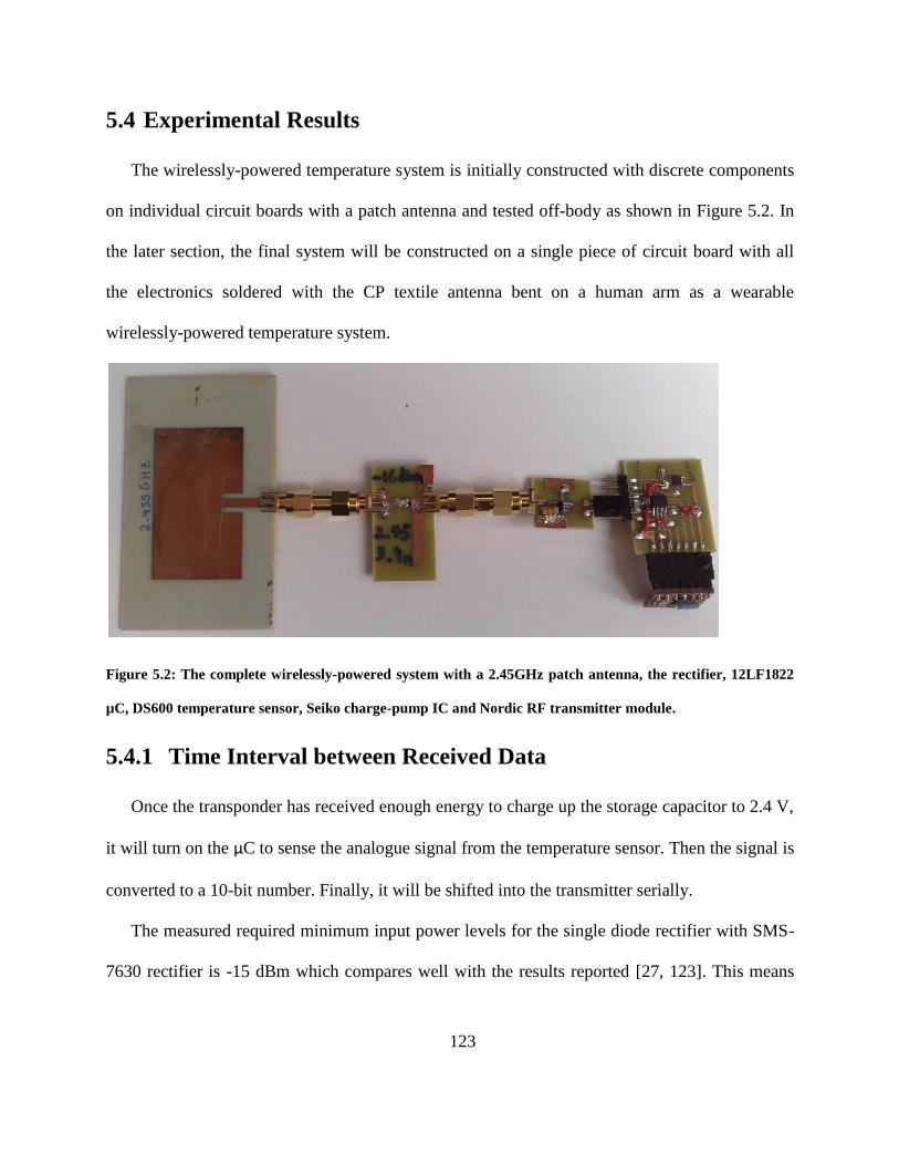
123
5.4 Experimental Results
The wirelessly-powered temperature system is initially constructed with discrete components
on individual circuit boards with a patch antenna and tested off-body as shown in Figure 5.2. In
the later section, the final system will be constructed on a single piece of circuit board with all
the electronics soldered with the CP textile antenna bent on a human arm as a wearable
wirelessly-powered temperature system.
Figure 5.2: The complete wirelessly-powered system with a 2.45GHz patch antenna, the rectifier, 12LF1822
µC, DS600 temperature sensor, Seiko charge-pump IC and Nordic RF transmitter module.
5.4.1 Time Interval between Received Data
Once the transponder has received enough energy to charge up the storage capacitor to 2.4 V,
it will turn on the µC to sense the analogue signal from the temperature sensor. Then the signal is
converted to a 10-bit number. Finally, it will be shifted into the transmitter serially.
The measured required minimum input power levels for the single diode rectifier with SMS-
7630 rectifier is -15 dBm which compares well with the results reported [27, 123]. This means

124
that the voltage sensitivity is about 40 mV for a 50 Ω system and only 32 µW is required to turn
on the whole wirelessly-powered system.
For the system using the low power temperature sensor (MAX6607), two 22 µF capacitors
(total 44 µF measured) are used as a power storage device for the charge-pump IC. On the other
hand, for the high power temperature sensor (DS600), three 22 µF capacitors (total 67 µF
measured) are used to deliver more power to the load at the expense of the charging time. The
minimum time intervals between samples received at the base station are recorded, summarized
in Table 5-1 and plotted in Figure 5.3.
Input Power
Level (dBm)
Minimum time interval
between samples
received with a 44 µF
capacitor (seconds)
Minimum time interval
between samples
received with a 67 µF
capacitor (seconds)
-4 1.7 2.5
-5 2.1 3.1
-6 2.5 3.7
-7 3.1 4.6
-8 3.9 5.8
-9 4.9 7.4
-10 6.4 10
-11 8.6 13.3
-12 12.1 18.8
-13 18.2 29.2
-14 30.6 50.7
-15 70.3 135.8
Table 5-1: The minimum time intervals between samples received at the base station.
As shown in Figure 5.3, at an input power level of -4 dBm, the charge time for both
capacitors are reasonably fast, although the difference in sample interval is about 47%. At an
input power level of -10 dBm, the sample interval is 6.4 second and 10 second for 44 µF and 67

125
µF storage capacitors respectively. This means it takes approximately 56% longer to charge up
the larger capacitor to drive a bigger load. At an input power level of -15 dBm, the charge time is
increased dramatically to 135s for a 67 µF storage capacitor which is almost 2 times longer than
for the 44 µF counterpart.
Figure 5.3: The minimum time interval versus input power for received samples from the transponder.
Note that Table 5-1 shows the minimum time interval between samples received, but there is
a chance that the packet is corrupted by signals from the environment such as WiFi signals or
background noise. In practice, the interval between samples can be longer than shown in the
table due to packet corruption.
5.4.2 Power Efficiency of the System
The efficiencies of the overall system at different power levels with a load resistance of 180
Ω are measured. The 180 Ω load is chosen because the µC with the RF transmitter has similar
input resistance when it is transmitting the sensor signal back to a base station. The storage
capacitor recharge interval represents the idle time of the µC because the charge-pump IC takes
time to charge up the 44 µF storage capacitor to 2.4 V. At the lowest operational input power
6.4
70.3
10
135.8
0.0
20.0
40.0
60.0
80.0
100.0
120.0
140.0
-15 -13 -11 -9 -7 -5
Sam
ple
s In
terv
al (
seco
nd)
Input Power Level (dBm)
44 µF Storage Capacitor 67 µF Storage Capacitor

126
level of -15 dBm, it takes the charge-pump IC about 70 seconds to charge up the capacitor to 2.4
V to turn on the µC. However, at an input power level of -10 dBm, it only takes about 6.4
seconds to charge up the storage capacitor. The measurable efficiencies within the harvester are
defined in Chapter 2.
The power efficiencies of different sections of the system based on Table 5-2 are plotted in
Figure 5.4. The lowest operational input power level of the single diode rectifier with SMS-7630
is -15 dBm and the total system efficiency is 2.6%. The charge-pump IC efficiency is decreasing
from 52% to 32% as the power level is increasing except when the power level is at -15 dBm due
to the fact that it is barely turned on. The rectifier efficiency is increasing as the power level is
increasing at a decreasing rate up to maximum of 27%. The system efficiency increases with a
decreasing rate as the power level increases beyond -9 dB as the efficiency of the charge-pump
IC decreases faster than the efficiency of the rectifier increases. The total system efficiency
reaches 9.2% when the input power is -9 dBm.
Input Power Level
(dBm)
Rectifier
Efficiency (%)
Charge-pump IC
Efficiency (%) System Efficiency (%)
-4 26.5 31.8 8.42
-5 26.7 32.1 8.58
-6 27.1 33.5 9.08
-7 25.1 36.8 9.21
-8 23.3 39.6 9.22
-9 23.2 39.8 9.24
-10 21 42.3 8.91
-11 17.7 47.1 8.34
-12 15.7 47.6 7.47
-13 13.1 47.7 6.25
-14 9 51.7 4.68
-15 8 32.2 2.56
Table 5-2: The power efficiency of different input power levels.
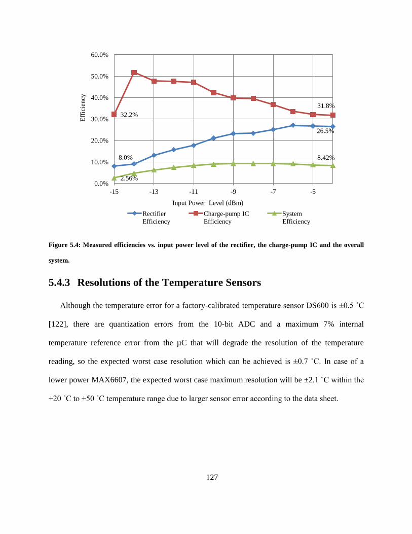
127
Figure 5.4: Measured efficiencies vs. input power level of the rectifier, the charge-pump IC and the overall
system.
5.4.3 Resolutions of the Temperature Sensors
Although the temperature error for a factory-calibrated temperature sensor D 600 is ±0.5 ˚C
[122], there are quantization errors from the 10-bit ADC and a maximum 7% internal
temperature reference error from the µC that will degrade the resolution of the temperature
reading, so the expected worst case resolution which can be achieved is ±0.7 ˚C. In case of a
lower power MAX6607, the expected worst case maximum resolution will be ±2.1 ˚C within the
20 ˚C to 50 ˚C temperature range due to larger sensor error according to the data sheet.
8.0%
26.5%
32.2%
31.8%
2.56%
8.42%
0.0%
10.0%
20.0%
30.0%
40.0%
50.0%
60.0%
-15 -13 -11 -9 -7 -5
Eff
icie
ncy
Input Power Level (dBm)
Rectifier
Efficiency
Charge-pump IC
Efficiency
System
Efficiency
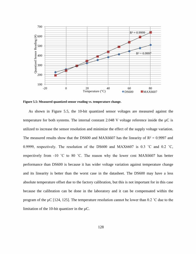
128
Figure 5.5: Measured quantized sensor reading vs. temperature change.
As shown in Figure 5.5, the 10-bit quantized sensor voltages are measured against the
temperature for both systems. The internal constant 2.048 V voltage reference inside the µC is
utilized to increase the sensor resolution and minimize the effect of the supply voltage variation.
The measured results show that the DS600 and MAX6607 has the linearity of R² = 0.9997 and
0.9999, respectively. The resolution of the D 600 and MAX6607 is 0.3 ˚C and 0.2 ˚C,
respectively from -10 ˚C to 80 ˚C. The reason why the lower cost MAX6607 has better
performance than DS600 is because it has wider voltage variation against temperature change
and its linearity is better than the worst case in the datasheet. The DS600 may have a less
absolute temperature offset due to the factory calibration, but this is not important for in this case
because the calibration can be done in the laboratory and it can be compensated within the
program of the µC [124, 125]. The temperature resolution cannot be lower than 0.2 ˚C due to the
limitation of the 10-bit quantizer in the µC.
R² = 0.9997
R² = 0.9999
100
200
300
400
500
600
700
-20 0 20 40 60 80
Quan
tize
d S
enso
r R
ead
ing (
#)
Temperature (°C) DS600 MAX6607

129
5.4.4 Performance of the Wirelessly-Powered Temperature Sensor
System
The comparison of our work to the other monolithic temperature sensors is shown in Table
5-3. Due to the high threshold voltage of 0.25 µm CMOS technology, the power sensitivity of
the monolithic solutions is only up to -12.5 dBm. However, the RF sensitivity of our power
harvester is -15 dBm and it is best in Table 5-3 due to the combination of a highly efficient
Schottky diode and an ultra-low input voltage Seiko charge-pump IC. The 900 MHz and 450
MHz monolithic solutions provide a better power consumption due to the integration of the
sensor and logic and lower transmission frequency. The major current consumption of this
system is due to the Nordic transceiver. Although the peak current consumption is 13 mA
according to the datasheet, it only happens over a very short period of time according to the
ShockBurst™ technology [118]. Therefore, the measured total system current consumption
whilst active is only 1.38 mA with the DS600 and µC running at 500 kHz. However, the current
consumption can be reduced by 13% by using a newer Nordic transceiver or by 19% using a
lower transmission power with the expense of higher data error rate [118, 126]. Note that extra
power has been consumed to compute the 16-bit CRC checksum for data integrity and a total of
56 bits are sent in each packet for each 32-bit data. Lowering the RF frequency can lead to a
longer operation range according to the Friis free space equation. However, the size of a 450
MHz or 900 MHz antenna is much bigger than its 2.45 GHz counterpart.

130
References This work [127] [25] [26]
RF Power Frequency 2.45 GHz 900 MHz 450 MHz
Sensitivity (dBm) -15 -12.3 -12.5
Maximum Output
Voltage
2.4 2 2.5
Temperature
Resolution (°C)
0.2 or 0.3
(-10 °C to 80 °C)
0.8
(-10 °C to 80 °C)
>0.8
(-14 °C to 40 °C)
Data Transmission
Method
32-bit data with
16-bit CRC
checksum + 8-bit
header
Backscattering frequency
modulation at 2.3
GHz
Current Consumption
during Active (mA)
1.4 1.1 1.1
Fabrication Process discrete
components on
FR-4
0.25µm CMOS +
Schottky diodes
0.25µm CMOS
Table 5-3: The performance comparisons of wirelessly-powered temperature sensors.
5.4.1 Range Test of the Wirelessly-Powered Temperature Sensor
System
The single diode rectifier with an SMS-7630 is incorporated to make a full rectenna system
using a 12 dBi gain 4x4 patch antenna array attached to a Rhode & Schwarz signal generator
with a 5 dBi gain single patch antenna attached to the transponder as shown in Figure 5.3. With
an RF power amplifier attached to the signal generator, it can radiate a total of 16.6 dBm (0.046
W) after power losses in the cabling to the anechoic chamber. The RF receiver is attached to a
logic analyzer for sample recording and the setup is shown in Figure 5.6.

131
Figure 5.6: The 2.45 GHz patch antenna array (on the left of the figure) is powering up the transponder
inside an anechoic chamber with a laptop receiving the temperature samples.
The longest measured operational distance is 2 metres. The measured power loss between the
antenna pair including the connectors is 30 dB with the maximum distance. Therefore the
received input RF power to the harvester is approximately -14 dBm. Additional power losses are
due to polarization and beam pattern mismatch between the two antennas. Based on these
measurements, according to the Friis transmission equation stated earlier, 1 W of transmitted
power can easily power the harvester over a few metres.
5.4.2 Range Test of the Wearable Wirelessly-Powered Temperature
Sensor System with the Textile Antenna
Lastly, the final system is assembled on a single PCB for a better mobility as a wearable
sensor system as shown in Figure 5.7a. The textile antenna is bent and attached to the
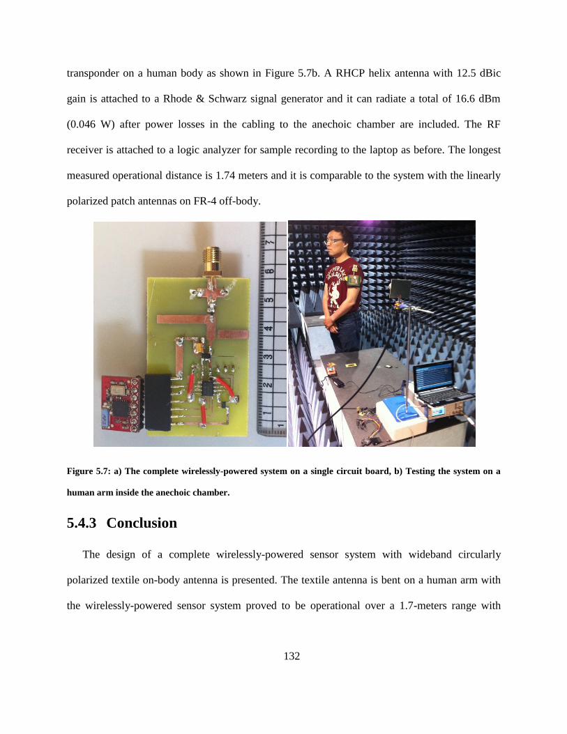
132
transponder on a human body as shown in Figure 5.7b. A RHCP helix antenna with 12.5 dBic
gain is attached to a Rhode & Schwarz signal generator and it can radiate a total of 16.6 dBm
(0.046 W) after power losses in the cabling to the anechoic chamber are included. The RF
receiver is attached to a logic analyzer for sample recording to the laptop as before. The longest
measured operational distance is 1.74 meters and it is comparable to the system with the linearly
polarized patch antennas on FR-4 off-body.
Figure 5.7: a) The complete wirelessly-powered system on a single circuit board, b) Testing the system on a
human arm inside the anechoic chamber.
5.4.3 Conclusion
The design of a complete wirelessly-powered sensor system with wideband circularly
polarized textile on-body antenna is presented. The textile antenna is bent on a human arm with
the wirelessly-powered sensor system proved to be operational over a 1.7-meters range with

133
under 0.05 W power transmitted from a base station. This demonstrates that a very low-cost and
ultra low-power battery-less µC sensor platform can be implemented and integrated into clothes
for other sensing applications in the future [14, 19, 128-130].

134
Chapter 6: Conclusion and Future Work
6.1 Conclusion
It has been demonstrated that a highly power sensitive rectifier at 2.45 GHz ISM band can be
constructed using off-the-shelf components. By combining a simple input impedance matching, a
1-stage rectifier and a charge-pump IC together, the power sensitivity level of -15 dBm is
achieved and it is very competitive with a standard CMOS solution.
A simple circularly-polarized antenna geometry has been investigated and it is found that the
single-sided wide-slot antenna not only features the wide impedance bandwidth, but it also has
the wide axial ratio bandwidth by using the simple tapered L-shaped feed line. The CPW feed
enables the whole antenna structure to be contained in a single layer of metal without an extra
layer for a ground plane. This design leads to a robust, compact and cost effective textile antenna
to be worn on a human body.
The circularly-polarized textile antenna is then optimized on single conductive layer with
proximity to a human body. Due to its wideband characteristics, it is able to accommodate the
shifting in central frequency due to effect of a human body and its wide impedance band is able
to cover the whole 2.45 GHz ISM band with a good purity of circular polarization. It is shown
that the performance of this CP textile antenna is significantly better than any other on-body CP
textile patch antennas have been reported.
Lastly, a complete wirelessly-powered temperature sensor system with the textile antenna is
constructed and worn on a human arm. It is shown that with just 50 mW of microwave power,

135
the system is able to operate at 1.74 metres and send the temperature data back to the laptop at a
regular time interval.
Therefore, this work presented in this thesis leads to a power sensitive and robust wearable
wirelessly-powered sensor system and it is ready to be applied to any other sensing applications
[129].
6.2 Future Work
This thesis concentrates on the antenna design for only on-body power transmission;
however, the antenna design to transmit energy to an implanted sensor at mid-field is still under
development in the community [131]. A wearable low frequency coil array for a near-field
energy transfer to band-aid sensor has been investigated, but optimized design for a such array at
microwave frequency to power up a mid-field implanted cardiac sensor is still not developed
[131]. Recently, it has been reported that the advantages using the 1.7 GHz over 200 MHz in
terms of the compactness and power efficiency in simulation as shown in Figure 6.1.
Figure 6.1: Wireless power transmission using 1.7 GHz (right) and 200 MHz (left). Red indicates more power
transmitted as shown in the right [131].

136
As the orientation of the antenna inside the body is unknown and changing, the powering
antenna outside the body should be CP so that the power transmission efficiency is unchanged
and independent to the orientations [132, 133]. Therefore, the CP textile antenna developed in
this thesis may be a possible candidate for the above application.
Figure 6.2: Wirelessly-powered ingestible camera from the Chinese University of Hong Kong [132].
Although the single feed CP antennas in Chapter 3 and 4 are very simple to implement and
have very wide impedance and axial ratio bandwidths; however the radiation with good axial
ratio only covers limited solid angle close to the centre of the antenna. A CP wide-slot antenna
with multiple feed lines has never been reported and it may significantly improve the solid angle
coverage with good axial ratio if the similar feeding structure of the wideband CP patch antenna
can be applied as shown in Figure 3.4 [74].

137
APPENDIX
//For RF2401A transmitter
/*
config_setup word 16 bits
23: 0 Payloads have an 8 bit address
22: 0
21: 1
20: 0
19: 0
18: 0
17: 1 16-Bit CRC
16: 1 CRC Enabled
15: 0 One channel receive
14: 1 ShockBurst Mode
13: 1 1Mbps Transmission Rate
12: 0
11: 1
10: 1
9: 1 RF Output Power
8: 0 RF Output Power
7: 0 Channel select (channel 2)
6: 0

138
5: 0
4: 0
3: 0
2: 1
1: 0
0: 0 Transmit mode (0=Tx, 1=Rx)
*/
#include <htc.h>
#define _XTAL_FREQ 2000000 // oscillator frequency for
_delay()
// Config: ext reset, no code protect, no brownout detect, no
watchdog,
// power-up timer enabled, 4MHz int clock
__CONFIG(MCLRE_OFF & CP_OFF & BOREN_OFF & WDTE_OFF & PWRTE_OFF
& FOSC_INTOSC);
#define TX_CE LATA1 //Enable transmission
#define TX_CS LATA0 //Enable configuration
#define TX_CLK1 LATA4 //Clocking for N2401
#define TX_DATA LATA5 //Data for N2401
#define SENSOR RA2 //Sensor input
unsigned char data_array[4]; //8-bit data
unsigned int count;
139
void configure_transmitter(void);
void transmit_data(void);
void main()
unsigned char dcnt; // delay counter
unsigned char i;
// Initialisation
TRISA = 0b000100; //Config RA2 as input
ANSA2 = 1; //RA2 as analogue sensor input
IRCF3 = 1; // 1101 4 MHz
IRCF2 = 1; // 1100 2 MHz
IRCF1 = 0; // 1011 1 MHz
IRCF0 = 0; // 0111 500kHz(default)
// configure ADC
ADCON1 = 0b01000011;
//0------- MSB of result in ADRESH<7> (ADFM = 0)
//-100---- Tad = Fosc/4 = 1 MHz)
//------00 Use VCC
//------11 Use internal Vref
ADCON0 = 0b00001001;
//-11101-- select temp sensor
//-11111-- FVR output
//-00001-- AN1

140
//-00010-- AN2
//-------1 turn ADC on (ADON = 1)
FVRCON = 0b10000010;
//1------- enable fixed voltage reference
//--1----- enable temperature sensor
//---0---- enable low range
//------10 ADC 2.048V fixed voltage ref
//------01 ADC 1.024V fixed voltage ref
//initialize the received data array
data_array[2] = 0x00;
data_array[3] = 0x00;
// Main loop
for (;;)
__delay_ms(1);
__delay_us(500);
//3ms requirement from powerup to active for n2401
//But can be smaller than 3 ms
configure_transmitter();
//configure the transmitter
GO_nDONE = 1; // start conversion
while (GO_nDONE) // wait until done
;

141
//10 bits result
data_array[0]= ADRESH; //Top 8-bit ADC result
data_array[1]= ADRESL; //Low 2-bit ADC result, MSB justified
data_array[2]= ADRESH; //Top 8-bit ADC result
data_array[3]= ADRESL; //Low 2-bit ADC result, MSB justified
__delay_ms(1);
__delay_us(500); //Can be smaller than 300us ~250us
transmit_data(); //We send 4 bytes
void configure_transmitter(void)
unsigned char i;
unsigned long config_setup;
//Config Mode
TX_CE = 0;
TX_CS = 1;
//Delay of 5us from CS to Data is taken care of by the for loop
//Setup configuration word, we only need upper 24 bits, zero pad
the lower 8 bits

142
config_setup = 0b00100011011011111111001000000000;
// ----------------1111001---------RF freq
// --------------10--------RF power 10 = -5db
// ----------1-----------------enable 1Mbps
// -------1------------------------CRC enable
// ------1-------------------------16 bit CRC
for(i = 0 ; i < 24 ; i++)
TX_DATA = (config_setup & 0x80000000) > 0; //Display
data
TX_CLK1 = 1;
TX_CLK1 = 0;
config_setup <<= 1 ; //shift 1 bit to left
//Configuration is active on falling edge of CS
TX_CE = 0;
TX_CS = 0;
//This sends out the data stored in the data_array
//data_array must be setup before calling this function
void transmit_data(void)

143
unsigned char i, j;
unsigned char temp, rf_address; //8-bit RF address
TX_CE = 1;
//Clock in address
rf_address = 0b11100111; //Power-on Default for all units
for(i = 0 ; i < 8 ; i++)
TX_DATA = (rf_address & 0x80) > 0; //Display data
TX_CLK1 = 1;
TX_CLK1 = 0;
rf_address <<= 1 ; //shift 1 bit to left
//Clock in the data_array
for(i = 0 ; i < 4 ; i++) //4 bytes
temp = data_array[i];
for(j = 0 ; j < 8 ; j++) //One bit at a time
TX_DATA = (temp & 0x80) > 0; //Display data
TX_CLK1 = 1;
TX_CLK1 = 0;
temp <<= 1; //shift 1 bit to left

144
TX_CE = 0; //Start transmission

145
BIBLIOGRAPHY
[1] C. M. Ghiglino, "Ultra-Wideband (UWB) rectenna design for Electromagnetic Energy
Harvesting," in Department of Signal Theory and Communications. Degree of Engineer
Catalonia: Polytechnic University of Catalonia, 2010.
[2] G. A. Vera, "Effcient Rectenna Design for Ambient Microwave Energy Recycling," in
Department of Signal Theory and Communications. Degree of Engineer Catalonia:
Polytechnic University of Catalonia 2009, p. 115.
[3] W. C. Brown, "The History of Power Transmission by Radio Waves," Microwave Theory
and Techniques, IEEE Transactions on, vol. 32, pp. 1230-1242, 1984.
[4] H. Jabbar, Y. S. Song, and T. T. Jeong, "RF energy harvesting system and circuits for
charging of mobile devices," Consumer Electronics, IEEE Transactions on, vol. 56, pp.
247-253, 2010.
[5] T. Paing, E. Falkenstein, R. Zane, and Z. Popovic, "Custom IC for Ultra-low Power RF
Energy Harvesting," in Applied Power Electronics Conference and Exposition, 2009.
APEC 2009. Twenty-Fourth Annual IEEE, 2009, pp. 1239-1245.
146
[6] T. Paing, J. Shin, R. Zane, and Z. Popovic, "Resistor Emulation Approach to Low-Power
RF Energy Harvesting," Power Electronics, IEEE Transactions on, vol. 23, pp. 1494-
1501, 2008.
[7] D. Masotti, A. Costanzo, and S. Adami, "Design and realization of a wearable multi-
frequency RF energy harvesting system," in Antennas and Propagation (EUCAP),
Proceedings of the 5th European Conference on, 2011, pp. 517-520.
[8] J. A. Hagerty, F. B. Helmbrecht, W. H. McCalpin, R. Zane, and Z. B. Popovic,
"Recycling ambient microwave energy with broad-band rectenna arrays," Microwave
Theory and Techniques, IEEE Transactions on, vol. 52, pp. 1014-1024, 2004.
[9] Y. Kawahara, K. Tsukada, and T. Asami, "Feasibility and potential application of power
scavenging from environmental RF signals," in Antennas and Propagation Society
International Symposium, 2009. APSURSI '09. IEEE, 2009, pp. 1-4.
[10] H. Nishimoto, Y. Kawahara, and T. Asami, "Prototype implementation of ambient RF
energy harvesting wireless sensor networks," in Sensors, 2010 IEEE, 2010, pp. 1282-
1287.
[11] H. Rajagopalan and Y. Rahmat-Samii, "Ingestible RFID bio-capsule tag design for
medical monitoring," in Antennas and Propagation Society International Symposium
(APSURSI), 2010 IEEE, 2010, pp. 1-4.

147
[12] K. Opasjumruskit, T. Thanthipwan, O. Sathusen, P. Sirinamarattana, P. Gadmanee, E.
Pootarapan, N. Wongkomet, A. Thanachayanont, and M. Thamsirianunt, "Self-powered
wireless temperature sensors exploit RFID technology," Pervasive Computing, IEEE, vol.
5, pp. 54-61, 2006.
[13] L. Yu-Te, Y. Huanfen, B. Parviz, and B. Otis, "A 3µW wirelessly powered CMOS
glucose sensor for an active contact lens," in Solid-State Circuits Conference Digest of
Technical Papers (ISSCC), 2011 IEEE International, 2011, pp. 38-40.
[14] D. J. Yeager, J. Holleman, R. Prasad, J. R. Smith, and B. P. Otis, "NeuralWISP: A
Wirelessly Powered Neural Interface With 1-m Range," Biomedical Circuits and
Systems, IEEE Transactions on, vol. 3, pp. 379-387, 2009.
[15] S. Pellerano, J. Alvarado, and Y. Palaskas, "A mm-wave power harvesting RFID tag in
90nm CMOS," in Custom Integrated Circuits Conference, CICC '09. IEEE, 2009, pp.
677-680.
[16] S. Pellerano, J. Alvarado, and Y. Palaskas, "A mm-Wave Power-Harvesting RFID Tag in
90 nm CMOS," Solid-State Circuits, IEEE Journal of, vol. 45, pp. 1627-1637, 2010.
[17] R. Vyas, V. Lakafosis, A. Rida, N. Chaisilwattana, S. Travis, J. Pan, and M. M.
Tentzeris, "Paper-Based RFID-Enabled Wireless Platforms for Sensing Applications,"
Microwave Theory and Techniques, IEEE Transactions on, vol. 57, pp. 1370-1382, 2009.

148
[18] N. Chaimanonart and D. J. Young, "Remote RF powering system for wireless MEMS
strain sensors," Sensors Journal, IEEE, vol. 6, pp. 484-489, 2006.
[19] J. Yoo, Y. Long, L. Seulki, K. Yongsang, and Y. Hoi-Jun, "A 5.2 mW Self-Configured
Wearable Body Sensor Network Controller and a 12 µW Wirelessly Powered Sensor for
a Continuous Health Monitoring System," Solid-State Circuits, IEEE Journal of, vol. 45,
pp. 178-188, 2010.
[20] J. Olivo, S. Carrara, and G. De Micheli, "Energy Harvesting and Remote Powering for
Implantable Biosensors," Sensors Journal, IEEE, vol. 11, pp. 1573-1586, 2011.
[21] M. G. Gnoni, A. Rollo, and P. Tundo, "A smart model for urban ticketing based on RFID
applications," in Industrial Engineering and Engineering Management, 2009. IEEM
2009. IEEE International Conference on, 2009, pp. 2353-2357.
[22] C. Narrijun, S. Seong-Jun, L. Jae-Youl, K. Sunyoung, K. Shiho, and Y. Hoi-Jun, "A 8
µW, 0.3-mm2 RF-powered transponder with temperature sensor for wireless
environmental monitoring," in Circuits and Systems, 2005. ISCAS 2005. IEEE
International Symposium on, 2005, pp. 4763-4766 Vol. 5.
[23] U. Karthaus and M. Fischer, "Fully integrated passive UHF RFID transponder IC with
16.7µW minimum RF input power," Solid-State Circuits, IEEE Journal of, vol. 38, pp.
1602-1608, 2003.
149
[24] T. Le, K. Mayaram, and T. Fiez, "Efficient Far-Field Radio Frequency Energy
Harvesting for Passively Powered Sensor Networks," Solid-State Circuits, IEEE Journal
of, vol. 43, pp. 1287-1302, 2008.
[25] F. Kocer and M. P. Flynn, "An RF-powered, wireless CMOS temperature sensor,"
Sensors Journal, IEEE, vol. 6, pp. 557-564, 2006.
[26] J. Ghalibafan and F. H. Kashani, "A circularly polarized fractal microstrip antenna for
RFID applications," in Radio-Frequency Integration Technology, RFIT 2009. IEEE
International Symposium on, 2009, pp. 319-322.
[27] G. A. Vera, A. Georgiadis, A. Collado, and S. Via, "Design of a 2.45 GHz rectenna for
electromagnetic (EM) energy scavenging," in Radio and Wireless Symposium (RWS),
2010 IEEE, pp. 61-64.
[28] Z. Harouni, L. Cirio, L. Osman, A. Gharsallah, and O. Picon, "A Dual Circularly
Polarized 2.45-GHz Rectenna for Wireless Power Transmission," Antennas and Wireless
Propagation Letters, IEEE, vol. 10, pp. 306-309, 2011.
[29] W. Zheyu, Z. Lanlin, D. Psychoudakis, and J. L. Volakis, "Flexible textile antennas for
body-worn communication," in Antenna Technology (iWAT), 2012 IEEE International
Workshop on, 2011, pp. 205-208.

150
[30] P. J. Soh, G. A. E. Vandenbosch, S. L. Ooi, and M. R. N. Husna, "Wearable dual-band
Sierpinski fractal PIFA using conductive fabric," Electronics Letters, vol. 47, pp. 365-
367, 2011.
[31] E. K. Kaivanto, M. Berg, E. Salonen, and P. de Maagt, "Wearable Circularly Polarized
Antenna for Personal Satellite Communication and Navigation," Antennas and
Propagation, IEEE Transactions on, vol. 59, pp. 4490-4496, 2011.
[32] R. Jung-Sim, C. Yong-Seung, L. Jae-Hee, T. Youndo, N. Sangwook, and K. Tae Jin,
"Embroidered Wearable Multiresonant Folded Dipole Antenna for FM Reception,"
Antennas and Wireless Propagation Letters, IEEE, vol. 9, pp. 803-806, 2010.
[33] T. F. Kennedy, P. W. Fink, A. W. Chu, N. J. Champagne, G. Y. Lin, and M. A. Khayat,
"Body-Worn E-Textile Antennas: The Good, the Low-Mass, and the Conformal,"
Antennas and Propagation, IEEE Transactions on, vol. 57, pp. 910-918, 2009.
[34] A. Tronquo, H. Rogier, C. Hertleer, and L. Van Langenhove, "Robust planar textile
antenna for wireless body LANs operating in 2.45 GHz ISM band," Electronics Letters,
vol. 42, pp. 142-143, 2006.
[35] P. Salonen, K. Jaehoon, and Y. Rahmat-Samii, "Dual-band E-shaped patch wearable
textile antenna," in Antennas and Propagation Society International Symposium, 2005
IEEE, pp. 466-469 Vol. 1A.
151
[36] H. Giddens, D. L. Paul, G. S. Hilton, and J. P. McGeehan, "Influence of body proximity
on the efficiency of a wearable textile patch antenna," in Antennas and Propagation
(EUCAP), 2012 6th European Conference on, pp. 1353-1357.
[37] P. Salonen and Y. Rahmat-Samii, "Textile antennas: Effects of antenna bending on input
matching and impedance bandwidth," in Antennas and Propagation, EuCAP 2006. First
European Conference on, 2006, pp. 1-5.
[38] S. Dey, N. Saha, and S. Biswas, "Design and performance analysis of UWB circular disc
monopole textile antenna and bending consequences," in Antennas and Propagation
(EUCAP), Proceedings of the 5th European Conference on, 2011, pp. 1129-1133.
[39] Y. Fei and N. Soltani, "Design techniques for power harvesting of passive wireless
microsensors," in Circuits and Systems, MWSCAS 2008. 51st Midwest Symposium on,
2008, pp. 289-293.
[40] A. Shameli, A. Safarian, A. Rofougaran, M. Rofougaran, and F. De Flaviis, "Power
Harvester Design for Passive UHF RFID Tag Using a Voltage Boosting Technique,"
Microwave Theory and Techniques, IEEE Transactions on, vol. 55, pp. 1089-1097, 2007.
[41] N. Soltani and Y. Fei, "A High-Gain Power-Matching Technique for Efficient Radio-
Frequency Power Harvest of Passive Wireless Microsystems," Circuits and Systems I:
Regular Papers, IEEE Transactions on, vol. 57, pp. 2685-2695, 2010.

152
[42] E. Bergeret, J. Gaubert, P. Pannier, and P. Rizzo, "Power generation system for UHF
passive RFID," Electronics Letters, vol. 42, pp. 1452-1454, 2006.
[43] D. Pozar, Microwave Engineering, 2005.
[44] Hewlett-Packard Corp., "Surface Mount Microwave Schottky Detector Diodes," 1999.
[45] Skyworks Solutions Inc., Surface Mount mixer and Detector Schottky Diodes, 2010.
[46] Skyworks Solutions Inc., Data sheet - Surface Mount Mixer and Detector Schottky
Diodes, 2010.
[47] AWR Corp., "www.awrcorp.com.", 2010.
[48] Agilent Technology, Surface mount zero bias Schottky detector diodes technical data,
1999.
[49] Mega Electronics, "www.megauk.com.", 2012.
[50] Rogers Corporation, RO4000 Series high Frequency circuit Materials Data Sheet, 2006.

153
[51] S. Riviere, A. Douyere, F. Alicalapa, and J. D. L. S. Luk, "Study of complete WPT
system for WSN applications at low power level," Electronics Letters, vol. 46, pp. 597-
598, 15/4/2010 2010.
[52] A. Douyere, J. D. Lan Sun Luk, and F. Alicalapa, "High efficiency microwave rectenna
circuit: modelling and design," Electronics Letters, vol. 44, pp. 1409-1410, 2008.
[53] Hewlett-Packard Co., Linear Models for Diode Surface Mount Packages Application
Note 1124, 1997.
[54] Seiko Instruments Inc., S-882Z Series Ultra-low voltage operation charge pump IC for
step-up DC-DC converter startup, 2010.
[55] K. W. Lui, A. Vilches, and C. Toumazou, "Ultra-efficient microwave harvesting system
for battery-less micropower microcontroller platform," Microwaves, Antennas &
Propagation, IET, vol. 5, pp. 811-817, 2011.
[56] P. J. Bevelacqua, "www.antenna-theory.com.", 2012.
[57] T. S. Bird, "Definition and Misuse of Return Loss [Report of the Transactions Editor-in-
Chief]," Antennas and Propagation Magazine, IEEE, vol. 51, pp. 166-167, 2009.
154
[58] C. Yue-Ying, J. Yong-Chang, Z. Gang, Z. Wei, and X. Huan-Huan, "A novel compact
slot antenna for broadband circularly polarized radiation," in Antennas Propagation and
EM Theory (ISAPE), 2010 9th International Symposium on, 2010, pp. 201-204.
[59] J. Pourahmadazar and S. Mohammadi, "Compact circularly-polarised slot antenna for
UWB applications," Electronics Letters, vol. 47, pp. 837-838, 2011.
[60] H. A. Ghali and T. A. Moselhy, "Broad-band and circularly polarized space-filling-based
slot antennas," Microwave Theory and Techniques, IEEE Transactions on, vol. 53, pp.
1946-1950, 2005.
[61] Nasimuddin, C. Zhi Ning, and Q. Xianming, "Symmetric-Aperture Antenna for
Broadband Circular Polarization," Antennas and Propagation, IEEE Transactions on,
vol. 59, pp. 3932-3936, 2011.
[62] M. Khalily, M. K. A. Rahim, and A. A. Kishk, "Planar Wideband Circularly Polarized
Antenna Design With Rectangular Ring Dielectric Resonator and Parasitic Printed
Loops," Antennas and Wireless Propagation Letters, IEEE, vol. 11, pp. 905-908, 2012.
[63] X.-y. Zhang, S. Lin, Y.-d. Wang, S.-y. Liu, X.-y. Zhang, W.-b. Zhang, and J.-x. Wang,
"Broadband circularly polarized antenna with a T-type fractal boundary wide-slot and a
L-shaped strip," in Microwave Conference Proceedings (CJMW), 2011 China-Japan
Joint, 2011, pp. 1-3.

155
[64] H. Wang-Ta, C. Tze-Hsuan, and K. Jean-Fu, "Dual-Band Circularly Polarized Cavity-
Backed Annular Slot Antenna for GPS Receiver," Antennas and Propagation, IEEE
Transactions on, vol. 60, pp. 2076-2080, 2011.
[65] J. D. Kraus, Antennas for all applications: Mcgraw Hill, 2001.
[66] I. Locher, M. Klemm, T. Kirstein, and G. Troster, "Design and Characterization of Purely
Textile Patch Antennas," Advanced Packaging, IEEE Transactions on, vol. 29, pp. 777-
788, 2006.
[67] C. Hertleer, H. Rogier, L. Vallozzi, and L. Van Langenhove, "A Textile Antenna for Off-
Body Communication Integrated Into Protective Clothing for Firefighters," Antennas and
Propagation, IEEE Transactions on, vol. 57, pp. 919-925, 2009.
[68] D. Schaubert and D. Pozar, "Microstrip Antennas:The Analysis and Design of Microstrip
Antennas and Arrays ", 1995, pp. 57-104.
[69] D. Pozar, Schaubert, D. , Microstrip Antennas:The Analysis and Design of Microstrip
Antennas and Arrays: Wiley-IEEE Press 1995.
[70] F. Yang, Z. Xue-Xia, Y. Xiaoning, and Y. Rahmat-Samii, "Wide-band E-shaped patch
antennas for wireless communications," Antennas and Propagation, IEEE Transactions
on, vol. 49, pp. 1094-1100, 2001.

156
[71] S. D. Targonski, R. B. Waterhouse, and D. M. Pozar, "Design of wide-band aperture-
stacked patch microstrip antennas," Antennas and Propagation, IEEE Transactions on,
vol. 46, pp. 1245-1251, 1998.
[72] S. D. Targonski and D. M. Pozar, "Design of wideband circularly polarized aperture-
coupled microstrip antennas," Antennas and Propagation, IEEE Transactions on, vol. 41,
pp. 214-220, 1993.
[73] R. Bancroft, Microstrip and Printed Antenna Design: SciTech publishing, Inc., 2004.
[74] G. Yong-Xin, K. Kah-Wee, and O. Ling Chuen, "Wideband Circularly Polarized Patch
Antenna Using Broadband Baluns," Antennas and Propagation, IEEE Transactions on,
vol. 56, pp. 319-326, 2008.
[75] W. Kin-Lu and C. Tzung-Wern, "Single-patch broadband circularly polarized microstrip
antennas," in Antennas and Propagation Society International Symposium, 2000. IEEE,
2000, pp. 984-987 vol.2.
[76] C. C. Chou, K. H. Lin, and H. L. Su, "Broadband circularly polarised crosspatch-loaded
square slot antenna," Electronics Letters, vol. 43, pp. 485-486, 2007.

157
[77] N. Felegari, J. Nourinia, C. Ghobadi, and J. Pourahmadazar, "Broadband CPW-Fed
Circularly Polarized Square Slot Antenna With Three Inverted-L-Shape Grounded
Strips," Antennas and Wireless Propagation Letters, IEEE, vol. 10, pp. 274-277, 2011.
[78] S. Jia-Yi and C. Wei-Hung, "Axial-Ratio-Bandwidth Enhancement of a Microstrip-Line-
Fed Circularly Polarized Annular-Ring Slot Antenna," Antennas and Propagation, IEEE
Transactions on, vol. 59, pp. 2450-2456, 2011.
[79] K. C. Hwang, "Broadband circularly-polarised Spidron fractal slot antenna," Electronics
Letters, vol. 45, pp. 3-4, 2009.
[80] T. Fukusako, R. Sakami, and K. Iwata, "Broadband circularly polarized planar antenna
using partially covered circular wide-slot and L-probe," in Microwave Conference,
APMC 2008. Asia-Pacific, 2008, pp. 1-4.
[81] S. Jia-Yi, C. I. G. Hsu, H. Min-Hua, O. Yu-He, and W. Ming-Ting, "Design of Circularly
Polarized Annular-Ring Slot Antennas Fed by a Double-Bent Microstripline," Antennas
and Propagation, IEEE Transactions on, vol. 55, pp. 3134-3139, 2007.
[82] S. Jia-Yi and W. Kin-Lu, "Bandwidth enhancement of a microstrip-line-fed printed wide-
slot antenna," Antennas and Propagation, IEEE Transactions on, vol. 49, pp. 1020-1024,
2001.

158
[83] J. Pourahmadazar, C. Ghobadi, J. Nourinia, N. Felegari, and H. Shirzad, "Broadband
CPW-Fed Circularly Polarized Square Slot Antenna With Inverted-L Strips for UWB
Applications," Antennas and Wireless Propagation Letters, IEEE, vol. 10, pp. 369-372,
2011.
[84] S. Jia-Yi, C. I. G. Hsu, C. Zhi-Wei, and C. Chi-Chaan, "Broadband CPW-Fed Circularly
Polarized Square Slot Antenna With Lightening-Shaped Feedline and Inverted-L
Grounded Strips," Antennas and Propagation, IEEE Transactions on, vol. 58, pp. 973-
977, 2010.
[85] S. Jia-Yi and C. Chi-Chaan, "Circularly Polarized Square Slot Antenna With a Pair of
Inverted-L Grounded Strips," Antennas and Wireless Propagation Letters, IEEE, vol. 7,
pp. 149-151, 2008.
[86] C. H. Chen, E. K. N. Yung, and B. J. Hu, "Miniaturised CPW-fed circularly polarised
corrugated slot antenna with meander line loaded," Electronics Letters, vol. 43, pp. 1404-
1405, 2007.
[87] V. P. Sarin, M. S. Nishamol, D. Tony, C. K. Aanandan, P. Mohanan, and K. Vasudevan,
"A Broadband L-Strip Fed Printed Microstrip Antenna," Antennas and Propagation,
IEEE Transactions on, vol. 59, pp. 281-284, 2011.

159
[88] A. R. El-Damak, H. Ghali, and H. F. Ragaie, "Circularly polarized fractal slot antenna,"
in Microwave Conference, 2005 European, 2005, p. 4 pp.
[89] Y. Sai Ho, M. Kim Fung, and C. Wing Shing, "A Bandwidth Improved Circular
Polarized Slot Antenna Using a Slot Composed of Multiple Circular Sectors," Antennas
and Propagation, IEEE Transactions on, vol. 59, pp. 3065-3070, 2011.
[90] Y. F. Liu, K. L. Lau, Q. Xue, and C. H. Chan, "Experimental studies of printed wide-slot
antenna for wide-band applications," Antennas and Wireless Propagation Letters, IEEE,
vol. 3, pp. 273-275, 2004.
[91] A. Dastranj, A. Imani, and M. Naser-Moghaddasi, "Printed Wide-Slot Antenna for
Wideband Applications," Antennas and Propagation, IEEE Transactions on, vol. 56, pp.
3097-3102, 2008.
[92] L. Fan, J. Yong-Chang, R. Li-Shi, G. Jin-Gang, and C. Bo, "Compact double T-shaped
slots antenna with a rectangular patch for bandwidth enhancement," in Antennas
Propagation and EM Theory (ISAPE), 2010 9th International Symposium on, pp. 286-
288.
[93] CST Computer Simulation Technology AG., "www.cst.com/.", 2010.
[94] ETS-Lindgren, Double Ridged Waveguide Horn Model 3115, 2007.

160
[95] M. Klemm and G. Troester, "Textile UWB Antennas for Wireless Body Area Networks,"
Antennas and Propagation, IEEE Transactions on, vol. 54, pp. 3192-3197, 2006.
[96] P. Salonen, Y. Fan, Y. Rahmat-Samii, and M. Kivikoski, "WEBGA - wearable
electromagnetic band-gap antenna," in Antennas and Propagation Society International
Symposium, 2004. IEEE, 2004, pp. 451-454 Vol.1.
[97] A. A. Serra, P. Nepa, and G. Manara, "A Wearable Two-Antenna System on a Life
Jacket for Cospas-Sarsat Personal Locator Beacons," Antennas and Propagation, IEEE
Transactions on, vol. 60, pp. 1035-1042, 2012.
[98] B. Sanz-Izquierdo, F. Huang, J. C. Batchelor, and M. Sobhy, "Compact Antenna for
WLAN on body applications," in Microwave Conference, 2006. 36th European, 2006,
pp. 815-818.
[99] "Antennas zip it up," Electronics Letters, vol. 47, pp. 1256-1256, 2011.
[100] D. Gaspar and A. A. Moreira, "Belt antenna for wearable applications," in Antennas and
Propagation Society International Symposium, APSURSI '09. IEEE, 2009, pp. 1-4.
[101] T. Kellomaki, "Effects of the Human Body on Single-Layer Wearable Antennas." vol.
Doctor of Science in Technology Tampere: Tampere University of Technology, 2012, p.
160.

161
[102] E. Kaivanto, J. Lilja, M. Berg, E. Salonen, and P. Salonen, "Circularly polarized textile
antenna for personal satellite communication," in Antennas and Propagation (EuCAP),
2010 Proceedings of the Fourth European Conference on, 2010, pp. 1-4.
[103] Larid Technology, "Metallized Conductive Products," p. 20, 2010.
[104] O. Yuehui and W. J. Chappell, "High Frequency Properties of Electro-Textiles for
Wearable Antenna Applications," Antennas and Propagation, IEEE Transactions on, vol.
56, pp. 381-389, 2008.
[105] R. W. L. S Gabriely, C Gabriel, "The dielectric properties of biological tissues: III.
Parametric models for the dielectric spectrum of tissues," Phys. Med. Biol., vol. 41, pp.
2271–2293, 1996.
[106] R. W. L. S Gabriely, C Gabriel, "The dielectric properties of biological tissues: II.
Measurements in the frequency range 10 Hz to 20 GHz," Phys. Med. Biol., vol. 41, pp.
2251–2269, 1996.
[107] S. G. S Gabriel, E Corthout, "The dielectric properties of biological tissues: I. Literature
survey," Phys. Med. Biol., vol. 41, pp. 2231-2249, 1996.

162
[108] Daniele Andreuccetti, "Calculation of the Dielectric Properties of Body Tissues in the
frequency range 10 Hz - 100 GHz." vol. 2012 Florence: ITALIAN NATIONAL
RESEARCH COUNCIL.
[109] Michael J. Ackerman, "Visble Human Project.", U.S. National Library of Medicine,
2012.
[110] C. Hertleer, A. Tronquo, H. Rogier, L. Vallozzi, and L. Van Langenhove, "Aperture-
Coupled Patch Antenna for Integration Into Wearable Textile Systems," Antennas and
Wireless Propagation Letters, IEEE, vol. 6, pp. 392-395, 2007.
[111] M. Klemm, I. Locher, and G. Troster, "A novel circularly polarized textile antenna for
wearable applications," in Microwave Conference, 2004. 34th European, 2004, pp. 137-
140.
[112] G. A. Conway, W. G. Scanlon, and S. L. Cotton, "The performance of on-body wearable
antennas in a repeatable multipath environment," in Antennas and Propagation Society
International Symposium, 2008. AP-S 2008. IEEE, 2008, pp. 1-4.
[113] Microchip Technology Inc., PIC12F/LF1822/PIC16F/LF1823 Data Sheet, 2010.
[114] Texas Instruments, MSP430C11x1, MSP430F11x1A Mixed Signal Microcontroller,
2008.

163
[115] Microchip Technology Inc., PICkit™ 3 Programmer/Debugger User’s Guide, 2010.
[116] Microchip Technology Inc., MPLAB® IDE User’s Guide with MPLAB Editor and
MPLAB SIM Simulator, 2009.
[117] Microchip Technology Inc., HI-TECH C® for PIC10/12/16 User’s Guide, 2010.
[118] Nordic Semiconductor ASA, "Product Specification Single chip 2.4 GHz Transceiver
nRF2401A ": Nordic Semiconductor ASA, 2004.
[119] Sparkfun Electronics, "www.sparkfun.com/products/153.", 2012.
[120] Saleae LLC., "Saleae User Guide 1.1.15," 2012.
[121] Maxim Integrated Inc., "Low-Voltage Analog Temperature Sensors in SC70 and SOT23
Packages," 2001.
[122] Maxim Integrated Inc., "DS600 ±0.5C Accurate Analog-Output Temperature Sensor,"
2007.
[123] S. Riviere, A. Douyere, F. Alicalapa, and J. D. L. S. Luk, "Study of complete WPT
system for WSN applications at low power level," Electronics Letters, vol. 46, pp. 597-
598.
164
[124] Microchip Technology Inc., "AN1333 Use and Calibration of the Internal Temperature
Indicator," 2010.
[125] Microchip Technology Inc., "AN1001 IC Temperature Sensor Accuracy Compensation
with a PICmicro Microcontroller," 2005.
[126] Nordic Semiconductor ASA, "Product Specification Single chip 2.4 GHz Transceiver
nRF24L01," 2006.
[127] K. W. Lui, O. H. Murphy, and C. Toumazou, "32-µW Wirelessly-Powered Sensor
Platform With a 2-m Range," Sensors Journal, IEEE, vol. 12, pp. 1919-1924, Jun. 2012.
[128] C. Jiao, X. Lingli, M. Chao, L. Yong, X. Xiaoyuan, C. P. Yue, H. Zhiliang, and P. Y.
Chiang, "A near-threshold, multi-node, wireless body area sensor network powered by
RF energy harvesting," in Custom Integrated Circuits Conference (CICC), 2012 IEEE,
2012, pp. 1-4.
[129] T. J. D. M. McGrath, Wireless Sensor Networks for Healthcare Applications: Artech
House, 2010.
[130] N. Chaimanonart and D. J. Young, "An adaptively RF-powered wireless batteryless in
vivo EKG and core body temperature sensing microsystem for untethered genetically

165
engineered mice real-time monitoring," in Networked Sensing Systems (INSS), 2009 Sixth
International Conference on, 2009, pp. 1-6.
[131] J. S. H. Sanghoek Kim, Lisa Y. Chen, and Ada S. Y. Poon, "Wireless power transfer to a
cardiac implant," Appl. Phys. Lett., vol. 101, Aug. 13 2012.
[132] C. Yawen, M. Q. H. Meng, and W. Xiaona, "A prototype design of wireless capsule
endoscope," in Mechatronics and Automation, 2005 IEEE International Conference,
2005, pp. 400-403 Vol. 1.
[133] M. Rasouli, A. P. Kencana, H. Van An, E. Kiat, J. C. Y. Lai, and L. S. J. Phee, "Wireless
capsule endoscopes for enhanced diagnostic inspection of gastrointestinal tract," in
Robotics Automation and Mechatronics (RAM), 2010 IEEE Conference on, 2010, pp. 68-
71.