Embed Size (px)
Citation preview

A STUDY ON THE YIELD OF SELF-HEALING
CARBON NANOTUBE/NANOWIRE-BASED SYSTEM
By
JONGHO SEOL
Bachelor of Engineering
Samcheok National University
Samcheok, Korea
2000
Submitted to the Faculty of the Graduate College of the
Oklahoma State University in partial fulfillment of the requirements for
the Degree of MASTER OF SCIENCE
May, 2005

ii
A STUDY ON THE YIELD OF SELF-HEALING
CARBON NANOTUBE/NANOWIRE-BASED SYSTEM
Thesis Approved:
N. Park
Thesis Adviser K. M. George
V. Sarangan
A. Gordon Emslie
Dean of the Graduate College

iii
TABLE OF CONTENTS
Chapter Page 1. INTRODUCTION .....................................................................................................1 2. PRELIMINARIES AND REVIEW 2.1 Molecular Material.............................................................................................5 2.2 Structure of Carbon-Nanotubes .........................................................................5 2.3 Transistor, Diode, and NDRs.............................................................................9 2.4 Programmable Logic Array and Nanoarray Architecture................................15 3. SELF-HEALING CAPABILITY IN CARBON-NANOTUBES 3.1 Self-Healing Systems.......................................................................................21 3.2 Self-Healing Process........................................................................................22 3.3 Self-Healing Architecture ................................................................................24
4. DEFECT CHARACTERIZATION AND YIELD ANALYSIS .............................27 4.1 Expected Failure/Defects in Nanotube Array-based Architecture...................29 4.2 Yield with Redundancy Only...........................................................................35 4.3 Yield with Self-Healing ...................................................................................42 5. CONCLUSION.......................................................................................................46 REFERENCE...............................................................................................................56

1
CHAPTER 1
INTRODUCTION
Self-healing is a novel technology for repairing the failures/defects of modern
nanoprocessors to their original logic [16]. Until now this technology has been researched
for the purpose of using hardware/time redundancy to increase reliability of such systems
or yield of such systems [16]. For realizing self-healing, material for devices should be
changed to chemically organic components which are including carbon because existing
conventional silicon-based devices never have chemically organic properties. Even
though nanoelectronics are new technology, J. von Neumann published already one of the
first papers on nanoelectronics in 1956 [21].
This paper topic is "Probabilistic Logics and the Synthesis of Reliable Organisms from
Unreliable Components". In this von Neumann paper, static defects and dynamic failures
were issued because initially bad input or transient and intermittent failures occurred.
Neumann got a solution and proposed redundancy model for static defects with bad
inputs and dynamic failures with transient. A conventional fault tolerance systems uses
through space redundancy or time redundancy usually [22]. This fault tolerance gets over
expected number of failures/defects in manufactured devices for increasing its reliability

2
or yield. Spare processors in a processors array are usually idle or useless in normal
operation and they are used only after a failure is detected through periodic or diagnosis
and the processor array is reconfigured to include them [7]. Since the concept of self-
healing is inspired by human body healing system, the processing of self-healing
automatically is achieved by itself. The presented self-healing systems also use hardware
redundancy to increase reliability but they can have only minimum required spare
processors during self-healing processing to keep stable whole systems.
Self-healing must be performed by itself without any interruption or conscious input from
a human or external system and must repair failures/defects to original/normal.
In order to realize the process of self-healing, Carbon-nanotube must be used for wires to
assemble and interconnect assembled components in its architecture. Expected
failures/defects model have to be identified [16] in the Self-healing in Carbon-
nanotube/nanowire FET-based nanoarray systems.
Significant progress has been made in the area of nanoscale science and technology in the
past decade [17]. As one of the most interesting nanomaterials, Carbon-nanotubes
(CNTs) [11] have received significant attention in terms of fundamental properties,
measurements, and potential applications [17]. The Carbon nanotube has been researched
in physics and chemistry, and its self-healing capability has been developed. Extensive
research studies were stimulated, featuring purely experimental, theoretical, as well as
computer simulation approaches [8]. One of the striking features of CNTs is the potential
to use them in nanoscale devices due to their very interesting mechanical [8], optical as

3
well as electrical properties. Carbon Nanotubes will be one of the core and base of future
technology since Carbon Nanotubes devices have better properties than silicon based
devices. Many researchers of the carbon-nanotube have focused on electronic devices
which will be the next generation of devices [14]. Recently, researches have been focused
on the Carbon-nanotube's capability of self-healing.
In self-healing system, atoms in Carbon-nanotubes are excited to heal failures/defects and
restore normal structure when the structures are broken or defected [12, 23, 24]. The
advantages of Carbon nanotubes nanoarray-based architecture are first of all
miniaturization, fault tolerance, and nanoscale manufacuturing skill. In addition,
specially crossed nanoarray based architecture has a capability of self-healing in Carbon-
nanotubes. The disadvantage of Carbon-nanotube is not easy to connect with Silicon
based devices. Manufactured nanoscale architectures have to communicate with existed
typical silicon-based devices by using its interconnection wires. In nanoscale
architecture, there are a lot of defects/failures in Carbon-nanotube/wires and
failures/defects are expected at crossed point and contacted point with silicon nanowires
which is used as interconnecting wires in assembled nanoarray architecture usually. To
solve this problems fault tolerance used to reconfigure with redundant spare components
but it has a limitation in countless faults of devices. One of the important Carbon
properties is chemically self-bonding which can form molecular structures as nanotube. It
is possible to heal/repair failures and defects in the Carbon-nanotube. This healing
function by itself in Carbon-nanotube can reduce money and space for electronic devices.

4
The objective of this thesis is to identify self-healing in the Carbon-nanotube and develop
yield model. Also, this thesis will present failures/defects model characterization of
carbon-nanotubes and a self-healing process capability in such failures/defect systems.
Organization of this thesis is as follows. In section 2, preliminaries and review are
presented. Self-healing capability in carbon-nanotube is presented in section 3. A
proposed faults model characterization and yield analysis is presented in section 4.
Conclusion is discussed in section 5. Finally, references are in section 6.

5
CHAPTER 2
PRELIMINARIES AND REVIEW
2.1 Molecular Material In 1991, a tubular variant of the "bulkyball" carbon molecule was discovered by
Sumio Iijima of the NEC Fundamental Research Laboratory in Tsukuba, Japan [11]. It
has been called Carbon Nanotubes [11] (CNTs). Carbon Nanotubes (CNTs) is a
molecular material composed of carbon atoms which are bonded as hexagon structure
like a beehive. This interesing molecular material has mechanical and electrical
properties. Carbon nanotubes have very strong structure and conductor or semiconductor
properties. This molecular material, Carbon-nanotubes (CNTs), is enveloped around a
tube and has nanometer width as well as micrometers length at most [14].
2.2 Structure of Carbon-Nanotubes
A typical SWCNT (Single-Walled Carbon Nanotubes) structure is shown in Figure 2.1
[17]. This SWCNT is consisted of each node which has a carbon atom and lines are
bonded chemically [17]. A carbon atom and three bonding lines make one node. 1-2
nanometers in diameter and several micrometers in length are size of typical SWCNT
[19]. A SWCNT has interesting properties such as lightweight, thermal, mechanical, and
electrical properties.

6
A major feature of the SWCNT structure is the hexagon structrue look like a beehive that
it is possible to make a chemical self-bonding to form molecular structure of Carbon-
nanotubes. This chemical self-bonding property is achieved by atom excitation which is
happened by Carbon property when the hexagon pattern structure is broken. The basic
hexagon bonding structure has shown in Figure 2.2 [17]. One atom can be linked with
another neighbor atom to bond each other up to three neighbor atoms.
Figure 2.1: Molecular structure of Carbon-Nanotube
The bonding mechanism is based on molecular structure of Carbon-nanotubes which is
chemically linked and structured.

7
Figure 2.2: Basic hexagon bonded structure for one graphite
In Figure 2.3, single-walled carbon nanotube is structured by various ways. From one
graphite layer to single-walled carbon-nanotube, there is a regulation to express a roll-up
vector r and linear combinations of base vectors a and b [17].
r = na + mb
Where, n and m are integers.
Three different types of single-walled carbon-nanotube are defined by combinations of n
and m.
• m = 0, 'Zigzag',
• n = m, 'Armchair',
• Other, 'Chiral'.
Zigzag and Armchair these two structures are symmetrical structures and Chiral structure
is arranged as a spiral asymmetric structure. A single-walled carbon-nanotube is defined
by the vector which has two lines linked to two points (n, m). In case of Figure 2.1,
molecular structure has shown as a section of (10, 10) Carbon-nanotube. Various types of
Carbon-nanotubes have shown in Figure 2.4.

8
Armchair
Chiral
Zigzag
a
b
Figure 2.3: Definition of roll-up vector as linear combinations of base vectors a and b
[17]
Figure 2.4: Three structure types of Carbon Nanotubes [8]
Figure 2.5: Carbon Nanotube Molecular Structure (nanometer wide and micrometers
long) [20]

9
Carbon-nanotube is a molecular material composed of carbon atoms which are enveloped
around a tube and has nanometer in diameter and micrometers length at most [14]. Since
Carbon-nanotube is chemically bonded, it is strong and flexible than silicon based
devices. A typical carbon nanotube (CNT) molecular structure has shown in Figure 2.5.
Carbon- nanotube has not only mechanical properties but also electrical properties.
Carbon-nanotubes have various properties with their lattice geometry such as metals or
semiconductors [14]. Since Carbon-nanotube is thin and small with nanometer size and
micrometer long, we expect to design and manufacture more density and smaller devices.
Nanoscale architecture is proposed by Dehon [1]. Dehon proposed array-based
architecture for FET-based in nanoscale electronics. This architecture is based on
Carbon-nanotube and Silicon-nanowire and its size is extremely minimized and density.
This Dehon's proposed architecture has several important properties which are
minimization, fault tolerance, manufacturing skill [1]. In nanoscale architectures,
nanowires and nanotubes are used to configure tile type's logic as interconnected wires
[14]. Several tile types make mosaics which show crosspoints can be n-FET/p-FET
logic.
2.3 Transistors, Diodes, and NDRs
Nanowires and nanotubes can be used as not only interconnect wires but also active
devices such as transistors and diodes [14]. Carbon-nanowire diode is formed by a p-type
nanowire and an n-type nanowire at crossed point. A bipolar junction transistor is formed
by three nanowires with crossed wires. Memory or logic devices are formed with

10
assembled one or more crosspoints. Switched devices using suspended nanotubes have
shown by Lieber et al. This suspended nanotube switching devices has shown in Figure
2.6.
Suspended NT Connected Junction Disconnected junction
Support
Lower Conductor (Nanotube/Nanowire)
Figure 2.6: Suspended nanotube switching device [14]
In between the two states, they are stable each other with an energy barrier at crossed
nanotubes. This switched device using suspended nanotubes has two states which are ON
and OFF states. In OFF state, these tubes are isolated and mechanical forces keep their
distance to prevent the top wire going down to the lower wire. At that time, there are
very high resistances between the conductors (GΩ s) to keep their distance at crossed
point and the current between the crossed conductors is small because it has high
resistance between the conductors when the supplied voltage is same. In ON state, these
tubes are contacted and they have molecular power with a small resistance which is about
100 kΩ s between two tubes. Nanotube-nanowire FET device with Oxide coverd
nanowire has shown in Figure 2.7.

11
OxideCoveredNW
GatingNT or NW
Isd
Vg
Figure 2.7: Nanotube-nanowire FET device [1]
A nanowire which is doped can make FET such as p-type and n-type semiconductors. To
prevent direct electrical contact of a crossed conductor is used as growing the oxide over
the Silicon-nanowires. When the oxide thickness is increasing, Carbon-nanowire-diodes
can be made with 5V turn-on at the junctions and joule heating is oxidizing the junction
[9] shown in Figure 2.8.

12
Vo1
Vbias n-type NW
Vi1
Vo
Vi2 n
P-type NW
Vo1
VbiasFET
Vo
Vi1 Vi2
Figure 2.8: CNW-diode AND gate [14]
Vo1
Vi1
Vi2
Vo
Vbias
V01
Vi1
Vi2
Vo VbiasFET
Figure 2.9: CNW-FET NOR gate [14]
Carbon-nanowire-diodes can be used as ROM or logic arrays which have one time
programmable crosspoint or it can be used as an FET. Passing high current through a
low turn-on diode in air can increase the Oxide. In non-conducting region, Carbon-
nanowire-diodes perform as FETs. A p-type and n-type can be a p-channel crossed
nanowire FET. Carbon-nanowire-FET NOR gate has shown in Figure 2.9. This NOR-

13
FET gate was known as first reported nanoscale logic gate which has a voltage gain of 5
at room temperature [9, 14]. Using suspended nanotube as shown in Figure 2.6, the
switching device can be assembled as programmable diode OR array. The programmable
diode OR array has shown in Figure 2.10. In Figure 2.10 (a), black squares shows there is
no current that is OFF position suspended Nanotube. When programmed as "OFF", there
is high impedence on junction. The outputs Vout1 = in1 or in3 and Vout2 = in1 or in2.
In Figure 2.10 (b), assembled configurable OR planes used the suspended switching
when it is low resistance p-n junction, wires are connecting and when it is high
resistance, wires keep their distance as isolated. Molecular resonant tunneling diodes,
often called negative differential resistors (NDRs) have been actualized and it is called
NDRs [6]. These NDRs has a property of its own IV-curve. IV-curve of NDRs has
shown in Figure 2-11.

14
in0
in1
in2
in3
Vout1 Vout2
Gnd Gnd
Programmed "off"junctions are highimpedence.
Programmed "on"
Vpd(static load)
out1 =in1 or in3
out2 = in1 or in2
black squaresshow "off"position switches[no current flow]
in0
in1
in2
in3
"on" positionswitches
out1 out2
(a) (b)
Figure 2.10: Programmable diode OR array [1]
I peak
I valley
I
V peak V valley V
NDR region
Figure 2.11: I-V curve for a NDR (Negative Differential Resistors) device [14]

15
2.4 Programmable Logic Array and Nanoarray Architecture
Molecular Switches, the crossed nanoarrays are assembled by first layer linked from left
to right by flow directions, which is parallel array, and second layer linked from bottom
to top that is crossed arrays made by changing flow directions. The crossed arrays and
parallel arrays have shown in Figure 2.12.
flowPDMS mold
substrate8 paral lel arrays
first layer second layer 8 x 8 crossed arraysCrossed ar rays are made by changing flow direction
flow flow
Figure 2.12: Parallel array with single flows and crossed array with sequential crossed
flows [10]
At each Nanotube-Nanotube crosspoint (n, m), Carbon-nanotubes and nanowires form
assembled crossed nanoarray structures. The interconnection of the molecular scale wire

16
and tube are configured as switching devices at their crosspoints [1, 11]. Assembled
functional nanoarrays, programmable logic arrays, and interconnects have shown in
Figure 2.16.
The crossed functional nanoarrays at their crosspoints execute a programmed function as
programmable-logic-array and programmable interconnect [1, 11]. In Figure 2.13,
molecular switches at junction in crossed array of nanowire function as diode.
~ 50
nan
omet
ers
<----
- ----
------
-----
-->
Nanowires------------->
MolecullarSwitches
------
------
>
------
------
------
------
--->
Figure 2.13: Molecular switches at junction in crossed nanoarray [19]

17
The diameter of a nanowire is about 7.142 nanometers because the width is about 50
nanometers (as shown in Figure 2.13) when crossed array of nanowires are structured
with a crossed section of (4, 4) Carbon-nanotube. Usually the diameter of nanowires is
ranging from 6 to 20 nanometers and length of nanometer is ranging from 1 to 30
microns [14]. Parallel nanowires have space between two nanowires. This space width is
almost same as nanotubes regularily. The length of a nanotube in one PLA is about 112
nanometers because 8 nanotubes and 8 intervals between nanotubes in an 8 by 8 block.
Actually, it is difficult to evaluate nanoscale wires since the nanowires at crossed point
are interwined together [14].
The molecular-scale wires can be arranged into interconnected, crossed arrays with
molecular switching devices at their cross points. These crossed arrays can function as
programmable-logic arrays and programmable interconnect as shown in Figure 2.17
[1, 2]. The Programmable-Logic Arrays (PLAs) architecture has only both OR logic and
NOR logic because these logic combinations can make any arbitrary possible logic set.
In Figure 2.15, it shows how OR PLA and NOR PLA work respectively and together. In
this case, the output F1 is programmed to compute ((A1 OR C1) NOR (E3 OR F3)) and
the output F3 is programmed to compute ((B5 OR D5) NOR (D6 OR E6 OR G6)).
Another PLA can accept the output F1 and F3 as input through interconnections. Each
PLA is connected by interconnections which can reconfigure it. As shown in Figure 2.15
black dots in crossed array are connected as junction switch on. At cross point, molecular
devices are layered into crossed arrays as molecular switches or programmable diodes.
In Figure 2.14, molecular switches function as diode which is ON state or OFF state
followed by I-V characteristic.

18
"ON" State "OFF" State
I
V
(a) (b)
Figure 2.14: (a) A junction switch (b) A representative I-V characteristic [19]
A B C D E F G H F1 F2 F3 F4 F5 F6 F7 F8
OR Inteconnect NOR
Output F1 is programmed to compute (A1 OR C1) NOR (E3 OR F3)Output F3 is programmed to compute (B5 OR D5) NOR (D6 OR E6 OR G6)Output F1 and F3 can be used as inputs to other PLAs through interconnect. Output F1 and F3 are ready to send message to another PLA to computemore calculation or send message to output line.
8
7
6
5
4
3
2
1
Figure 2.15: Programmable Logic Array (OR and NOR) [19]

19
Figure 2.14(b) shows its I-V characteristic. This molecular switch has a representative I-
V characteristic. Assembled nanoarray architecture is consist of decodes, nanotubes,
microscaled wires, and PLAs (OR and NOR) as shown in Figure 2.17. In assembled
molecular-scale arrays, there are micro-scale wires to interconnect each PLAs and supply
power.
Programmable interconnect
PLA PLA PLA
PLA PLA PLA
PLA PLA PLA
Inteconnect is programmed used to address the cross-point in the arrayand provide power supply
Figure 2.16: Programmable Logic Arrays and Interconnect [19]

20
Decoder
Decoder
Decoder
Decoder
Decoder
De coder
Decoder
Decoder
OR NOR
NOR OR
Microscale Nanotube Wiring WiringInteconnet
----
->
----
->
PLA(Programmable Logic Array)
Figure 2.17: Assembled nanotube array-based architecture [1, 2]

21
CHAPTER 3
SELF-HEALING CAPABILITY IN CARBON-NANOTUBES
3.1 Self-healing Systems
Electric devices toward nanoscale, the self-healing in nanoscale devices is seriously
considered because devices are minimized and dense [24]. W. G. Bouricius et al called
"self-repair" [5] as the use of redundant components. Von Neumann proposed systems
that use modular redundancy [21] system performs a reconfiguration to heal a fault
component on permanent faults. Philip Koopman said it is too soon to say a real self-
healing and he proposed definition of term "self-healing". Philip Koopman defined self-
healing that such a system has to be able to heal itself without any input [16].
Typical fault-tolerance systems perform a reconfiguration to repair a system which has
permanent defects/failures, but reconfiguring system just use redundant component to
replace defect component to normal component. The self-healing system can heal defect
component and then recovered component re-used as normal component. Emerging of
Carbon-nanotube can realize self-healing systems. The system consisted of Carbon-
nanotube can heal failures/defects by itself when carbon-nanotube is broken. Where the
broken means that wire is short or wire is not working correctly because of the defect in

22
structure of nanotube. The broken wires can be used as recovered wires after healing, and
the hexagon pattern structure changed to pentagon structure.
3.2 Self-Healing Process
The self-healing is processing basically electronic excitation of atoms. Carbon-nanotube
has a hexagon structure pattern. When this hexagon structure lost one of atoms and linked
lines broken, the structure as its properties can be electronic excitation to bond broken
parts. Miyamoto et al theoretical approached and simulated the self-healing process. In
Figure 3.1(a), this nanotube is a section of (3, 3) with a monatomic vacancy. The self-
healing process is induced by electronic excitations [4, 22, 24].
0 fs 50 fs 100 fs 150 fs 200 fsmissingan atom and bonds
The electronic excitation makes new bonding after 200 femtoseconds.
New PentagonStructure
Femtosecond = 10 to -15 second.
Figure 3.1 Self-healing process with monatomic vacancy in nanotube [24]
When the vacancy happened in nanotube, there are three neighbor atoms and they can
create new bonding. A new bonding takes about 200 femto-seconds after atoms are

23
excited [24]. The self-healing process of vacancies in Carbon-nanotube induced by
electronic excitation never happens to Silicon-based devices [24].
In Figure 3.2, the left one is a monatomic vacancy and the right one is not a monatomic
vacancy but the arrangement of atoms is broken which shows the pentagon structure and
polygon having seven sides within the network of hexagon.
Figure 3.2: Defects in nanotubes [23]
Figure 3.3 shows change of structure induced by illumination or photo excitation. The
process of new bonding formation is only about 200 femto-seconds [24].
Figure 3.3: Defects in nanotubes and self-healing [23]

24
The atom network of a carbon-nanotube has a property which is capable of chemical self-
bonding to form a molecular structure. When the atom is removed or broken, the bonding
structure is also broken. The bonding structure is constructed from atom to atom as
hexagon pattern as usual. Even though one atom is removed, the atom network of carbon-
nanotube is activated and excited to bond each other. In Figure 3.4 a), a single atom has
removed in original nanotube and Figure 3.4 b) shows fault with single vacancy which
lost one atom and three adjusted bonded lines in original nanotube. In Figure 3.4 c),
above vacancy is fixed with pentagon bonding pattern and then one atom is moving to
right side from left hexagon pattern so they are reconnected in Figure 3.4 d).
Figure 3.4(d) shows a fixed atom network of a carbon-nanotube after healing process.
As shown Figure 3.4, there are four steps to heal vacancy (faults) part in nanotube [12].
a) b)
c) d)
Single atom removedFault with single vacany(lost one atom and three adjusted bonded lines)
Bonding a part of vacancy(pentagon structure)
Finishing bonding a vacancy(two pentagon structure)
Figure 3.4: Repairing a single vacancy [23]

25
• a) Original nanotube.
• b) Defect occurring with a single vacancy (one atom is removed).
• c) Bonding a part of vacancy (one pentagon bonding).
• d) Repairing and fixing the defect (two pentagon bonding).
3.3 Self-Healing Architecture
In this section, we consider assembled nanoarrays and how self-healing works in
architecture. In nanoscale array-based architecture, there exist some nanotubes which
have failures/defects and molecular junction switches can't function. In fault tolerance
system, usually to avoid faults their architecture is designed to tolerate these
failures/defects by both local wire sparing and array sparing. We present the concept of
self-healing in FET-based nanoarray in shown Figure 3.5. When expected faults occured
such as contact connection fails and broken or short, use adjacent spare line until repaired
by self-healing process to avoid system fails and to prevent wrong inputs into other
arrays. In original logic, there are five inputs A, B, C, D, E in array and there are also five
inputs as same as original logic in fault logic. Systems can use another spare line during
self-healing processing. This presented self-healing process needs a few spare wire and
array for self-healing processing but less than fault-tolerance model.

26
OR NOR
NOR OR
To avo id f ault inp ut du ring se lf-h ealing
fau ltsfau ltsfau ltsfau lts
Wh en fa ults occu r, systems p rogra mmed touse an othe r line to avoid faults. lin e e a nd line ihave f ault s an d the n line f and line j are conf igu red respectively.Fau lts ca n be repa ired by self-he aling pro cess as sho wn in Fig 3.1.
Original PLAs.No fa ults in arra ys.
a b c d e f g h i j k l m n o pa b c d e f g h i j k l m n o p
Dots are prog ramme d (en able d) conn ections.
OR NOR
NOR OR
Figure 3.5: Avoid failures and self-healing in Nanoarray Architecture [23]

27
CHAPTER 4
DEFECT CHARACTERIZATION AND YIELD ANALYSIS
In this chapter, we identify expected failures/defects in nanotube and compare the yield
of architecture with redundancy only and the nanotube-based architecture with self-
healing capability. First, we introduce and characterize a nanotube array-based
architecture under investigation. Then, we characterize the identified failures/defects in
each nanowire. Based on the characterization of the architecture and defects/failures, we
propose a yield model that can take into account redundancy along with self-healing
capability. In order to model and evaluate the yield of the architecture, we consider basic
single nanowire through extended architecture. Initially defects/failures in a single
nanowire will be considered and then the yield of single nanowire will be calculated.A
Single-PLA (Programmable Logic Array) architecture will be initially studied and then it
will be extend to a two-PLA architecture will be studied. The carbon-nanotube-based
PLA architecture has shown in Figure 4.1. To simplify diagram, it shows only a single
PLA (Programmable Logic Array). Finally we will generalize the yield model for general
cases.

28
Decoder
Decoder
OR
PLA
nanotube Microscaleinterconnect
Decoder
Figure 4.1 Carbon-Nanotube-based PLA [1, 20]

29
4.1 Expected Failures/Defects in Nanotube Array-based Architecture
In this section, we identify expected failures/defects in nanotube array-based architecture.
First, we consider the cross-point failure [20]. The architecture consists of an array of
PLA (Programmable Logic Array). Each PLA consist of row nanowires and column
nanowires in a mesh structure as shown in Figure 4.1. In Figure 4.1, each cross-point of
nanowires can function as diode (shown in Figure 2.14) and can be used as a
programmable switch. Each switch is set as "ON" status when suspended nanotube
(upper conductor) contacts lower nanotube (lower conductor) and "OFF" status when
suspended nanotube turn back to be separated. In this case, the upper nanotube
(conductor) has chance to meet expected failure such as broken and short when the upper
nanotube (conductor) is moving down to contact lower nanotube (conductor).

30
cross point failure
Lower conductor (nanotube) Connected junction
Suspendedupper conductor(nanotube)
Figure 4.2: Cross-point Failure [20]
Second, we consider the length failure [1, 20]. In order to extend the size and capacity of
nanoarray-based design, due to weak cross-point [20] along the nano-wire when an atom
is missing in a hexagon-shaped nanotube [24] has shown in Figure 4.3. The weak cross-
point [20] can't work correctly.
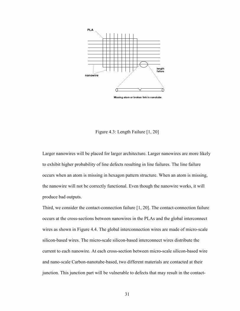
31
lengthfailure
Missing atom or broken link in nanotube
nanowire
PLA
Figure 4.3: Length Failure [1, 20]
Larger nanowires will be placed for larger architecture. Larger nanowires are more likely
to exhibit higher probability of line defects resulting in line failures. The line failure
occurs when an atom is missing in hexagon pattern structure. When an atom is missing,
the nanowire will not be correctly functional. Even though the nanowire works, it will
produce bad outputs.
Third, we consider the contact-connection failure [1, 20]. The contact-connection failure
occurs at the cross-sections between nanowires in the PLAs and the global interconnect
wires as shown in Figure 4.4. The global interconnection wires are made of micro-scale
silicon-based wires. The micro-scale silicon-based interconnect wires distribute the
current to each nanowire. At each cross-section between micro-scale silicon-based wire
and nano-scale Carbon-nanotube-based, two different materials are contacted at their
junction. This junction part will be vulnerable to defects that may result in the contact-

32
connection failure. Therefore, an adequate characterization and analysis on this type of
failure is necessary to ensure a high-yield nanoarray-based architecture to work its
function.
Decoder
Decoder
MicroscaleInterconnect Nanotube
wire
contact connection failure
address crosspoint in the arrayand power supply
broken nanowire
Figure 4.4: Contact-connection Failure [1, 20]
Lastly, we consider the contact decoder [20]. Decoding is the process of converting some
code such as binary code from nanowires into output value. Each nanowire is addressed
and activated through row and column decoder at the corresponding directions. When a
nanowire is addressed, the address (row and column addresses independently) is decoded
by the responsible decoder. A decoder is placed on each side of a PLA either for row and
column. When the addressed nanowires contact a decoder, the contacting point may be
defective as shown in Figure 4.5.

33
Decoder
Decoder
Decoder Connecting decoderFailure
nanowires
Figure 4.5: Contact Decoder Failure [20]
In order to ensure address decoding and architectural integrity of the nanowires, the
nanowires and the decoders have to establish a solid contact. We have shown all the each
expected defects/failures in a nanotube array-based PLA architecture in Figure 4.6.

34
The four kinds of failures/defects under investigation are further characterized as follows.
Along with a probability definition for each failure type of the yield modeling purpose is
as follow.
• Contact-connection failure: cP is the probability for each nanowire to experience
the contract-connection failure. The contact of a nanowire with a corresponding
microscale interconnect at one end of the nanowire is vulnerable to contact-
connection loss [1, 20].
• Length failure: lP is the probability for each nanowire to the length failure. As the
nanowire is longer, the nanowire may become more defective [1, 20].
• Cross-point failure: cpP is the probability for each nanowire to the cross-point
failure. The crossed nanowire at each cross-point is vulnerable to crossed-point of
row and column nanowires [20].
• Contact-decoder failure: dP is the probability for each nanowire to the contact-
decoder failure. As decoder is placed at each PLA, the contact of addressed
nanowire with the decoder at one end of nanowire is vulnerable to contact-
decoder loss [20].

35
Decoder
Decoder
MicroscaleInterconnect
Nanotubewire
contact decode failure
cross point failure
lengthfailure
contact connection failure
Figure 4.6: Defect characterization. Defects are defined as two types. One is contact
connection failure and another is length of nanotube failure. Contact connection failure;
1) nanotube connects decode 2) nanotube connects microscale interconnect 3) nanotubes
crossed at junction point. Lengths of nanotube failure 4) nanotube have short or break [1,
20]
4.2 Yield with Redundancy Only
In this section, we will study the yield of a nanotube array-based architecture with
defective-tolerance only and failure without self-healing capability. This nanotube array-
based architecture is using redundant (spare) nanotubes to avoid system faults when this

36
architecture has failures/defects in nanotube. From a Figure 2.15 previously shown in
chpater 2, for example, the original output F1 is programmed to compute (A1 OR C1)
NOR (E3 OR F3) and output F1 of using redundancy is programmed to compute (A2 OR
C2) NOR (E3 OR F3). When a failure occurs on the nanowire line number 1, we can use
a redundant nanowire number 2 in place of the failed line number 1. The result by using
the redundant nanowire is supposed to be the same as the original nanowire's output.
In order to get yield of redundancy only in nanotube array-based architecture, we
consider firstly a single nanowire line. In a single nanowire, the failure/defects will be
expected as we have mentioned in the previous section. First, we calculate the expected
yield of a single nanowire. The expected yield means the probability that the Carbon-
nanotubes in nanoarray-based architecture will be defect free. The yield of a single
nanowire, referred to as tubeP ,
D
d
CP
cp
L
l
C
ctube PPPPP )1()1()1()1( −×−×−×−= (4.1)
Where,
• C: numbers of contacts of nanowires with microscale interconnect at one end of
each nanowire.
• L: length of a nanowire.
• CP: number of cross-points. ncNULCP ×= )/(
• D: number of decodes. )/( ULD =
• U: unit length of a nanowire.
• icN : number of interconnects.

37
• ncN : number of cross-points in a unit length.
In order to get the yield of a single nanowire, tubeP we assume that all defects are 0.001 in
each defect. The result of simulation has shown in Figure 4.7.
Yield of a single nanotube
0
0.2
0.4
0.6
0.8
1
1.2
Length of nanotube (nm)
Yield
Yield of a single
nanotube
0 100 200 300 400 500 600 700 800 900 1000
Figure 4.7: Yield of tubeP vs. Length of nanowire
In chapter 2, Figure 2.17 has shown an example of a PLA which consists of 8 row
carbon-nanotubes and 8 column carbon-nanotubes. In order to get yield of a single
nanowire, we evaluate the impact of all possible defects and failures. For example, one
column nanowire in OR PLA connect to a row nanowire and then connect microscale
interconnect wire and finally connect decoder. Thus, so the yield of single nanowire tubeP
has to take all kinds of relevant defects/failures into account.

38
From Figure 4.1, we can get specific parameters such as C= 5, the number of contact of a
nanowire with microscale interconnect wire at one end, L=100nm, the length of wire,
CP=8, the number of cross-points, and D=1, the number of decoders. We can get also a
row nanowire as same manner.
Next, in order to extend yield of one an OR PLA, we consider how many nanowires are
being utilized as a quorum from n number of available nanowires in each direction in an
OR PLA by checking how many nanowires are addressed from $n$ number of column
and row nanowires, respectively. The yield of a column nanowire, columnY , can be
expressed as follows.
∑=
−−=
n
i
in
tube
i
tubecolumn PPinCY0
)1(),( (4.2)
Where,
• ),( inC : Number of combinations of choosing i nanowires out of n.
Based on the yield of column nanowires in an OR PLA, we extend the to a yield single
OR PLA level, by considering the yields of row and column nanowires together. From
the yield of column nanowires, the selected column nanowires can cross row nanowires
chosen from n number of row nanowires in the OR PLA. Then, we can calculate the
yield of an OR PLA yield. The net yield, referred to as netY , means that column and row
nanowires are taken together into account for the yield of a whole PLA. The yield of net
can be expressed as follows.
∑∑=
−
=
−=n
i
ijn
tube
ij
tube
n
j
net PPjnCinCY0 0
2
)1(),(),( (4.3)
Where,

39
• i: number of column nanowire chosen out of $n$ in OR PLA.
• j: of row nanowire chosen out of $n$ in OR PLA.
• n: number of row nanowire (column nanowire) in a single PLA.
• ij: number of ji× .
• 2n : number of n (number of row nanowire) n (number of column nanowire).
The variables i, j, n are defined and shown in Figure 4.8.
Decoder
Decoder
Decode r
Decoder
OR NOR
i chosen out of n
j chosen out of n
n
n
n
Figure 4.8: i and j in netY .
Next, in order to calculate the yield of two PLAs, i.e., OR and NOR, together, we select
the k nanowires in NOR (i.e., the second PLA in the model) based on the column
selection from the OR PLA (i.e., the first PLA in the model), j and then take k crossed
with j nanowires from n number of nanowires in NOR PLA. The yield of OR and NOR
PLA together is as follows.
∑ ∑∑= =
−−
=
−−=n
i
n
k
kjn
tube
kj
tube
ijn
tube
ij
tube
n
j
net PPknCPPjnCinCY0 00
22
)1(),()1(),(),( (4.4)

40
Where,
• i: number of column nanowire chosen out of n in OR PLA.
• j: number of row nanowire chosen out of n in NOR PLA from OR PLA.
• k: number of column nanowire chosen out of n in NOR PLA.
• ij: number of ji× .
• 2n : number of n (number of row nanowire) × n (number of column nanowire).
The variables i, j, n, and k are defined and shown in Figure 4.9.
Decoder
Decoder
Decoder
De coder
OR NOR
k chosen out of n
n
n
n
i chosen out of n
j chosen out of n
Figure 4.9: i, j, and k in rY .
The rT model is extendible to any larger scale of PLA-array in an incremental manner.
From example, we can add one more OR PLA resulting in an array of 3 PLAs, such that

41
OR, NOR, OR PLAs are interconnected alternately. Then, the new extended yield,
referred to as eY , can be expressed as follows. So this architecture has 3 tuples (OR, NOR,
OR). We can calculate eY similar to rY .
∑=
−−=
n
l
lkn
tube
lk
tubere PPlnCYY0
2
)1(),( (4.5)
• k: number of column nanowire chosen out of n in NOR PLA.
• l: number of row nanowire chosen out of n in NOR PLA.
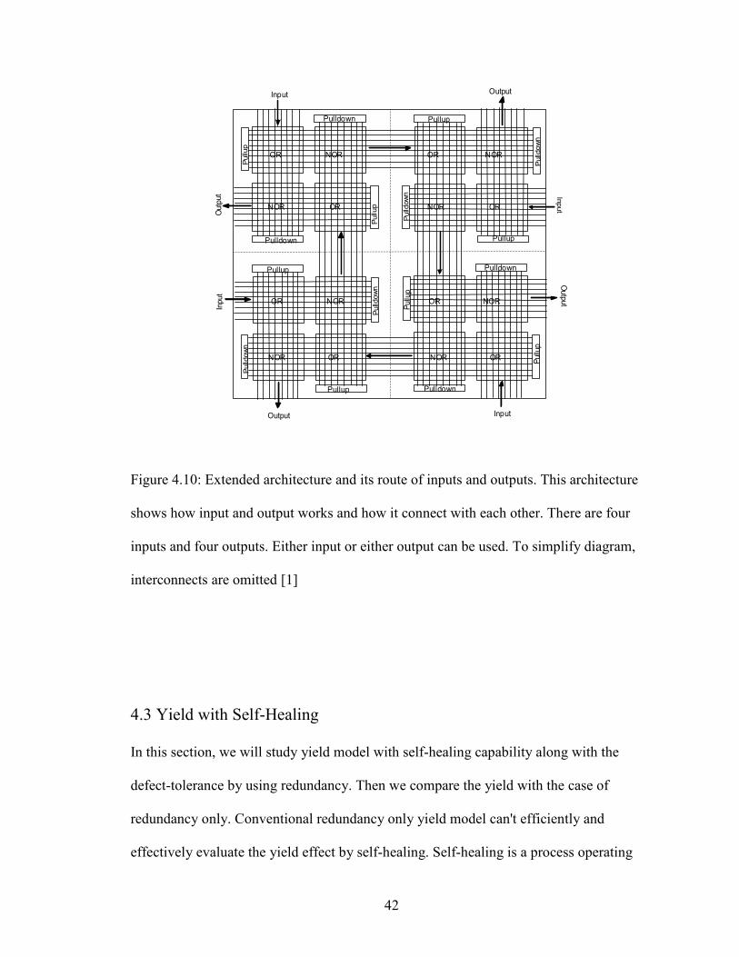
Extended PLAs is shown in Figure 4.10. Based on the converter of direction as shown in
Figure 4.10, we can calculate the yield of four PLAs model, referred to as gY , as follows.
∑ ∑= =
−−−−=
n
l
n
m
mln
tube
ml
tube
lkn
tube
lk
tuberg PPmnCPPlnCYY0 0
22
)1(),()1(),( (4.6)
Where,
• l: number of row nanowire chosen out of n in NOR PLA.
• m: number of column nanowire chosen out of n in OR PLA.
42
Pulldown
Pulldown
Pulldown
Pullup
Pullup
Pullup Pulldown
Pullup
Pullu
p
Pullu
p
Pulld
ow
n
Pulld
ow
n
Pulld
ow
n
Pulld
ow
n
Pullu
p
Pull u
p
OutputInput
OR NOR OR NOR
NOR OR NOR OR
NOR OR NOR OR
OR NOR OR NOR
InputOutput
Outp
ut
Outp
ut
Input
Input
Figure 4.10: Extended architecture and its route of inputs and outputs. This architecture
shows how input and output works and how it connect with each other. There are four
inputs and four outputs. Either input or either output can be used. To simplify diagram,
interconnects are omitted [1]
4.3 Yield with Self-Healing
In this section, we will study yield model with self-healing capability along with the
defect-tolerance by using redundancy. Then we compare the yield with the case of
redundancy only. Conventional redundancy only yield model can't efficiently and
effectively evaluate the yield effect by self-healing. Self-healing is a process operating

43
about 200 femto-second for bonding a new structure. In order to tolerate any other
intermediate failures, this architecture still has to rely on hardware redundancy along with
self-healing process. But the required amount of redundancy in self-healing system must
be much less than the one with redundancy only. The system with redundancy only can
not guarantee of continued system operation when failures occur more than the capacity
of spare hardware. But the self-healing system can release the redundant resources after
rebuilding its failed devices through self-healing. Hence, eventually the redundancy in
self-healing system can participate in the normal operation as well. Ultimately, this will
significantly improve the capacity and utilization of the system. This is the most
distinguished feature and benefit of self-healing systems. The yield model for self-healing
systems, referred to as shY , can be expressed as follows.
shggsh YYY α×−+= )1( (4.7)
Where,
• gY : Yield with redundancy only.
• shα : Rate that self-healing capability will repair defects correctly.
In the self-healing yield model, shY , we consider the yield loss, i.e., gY−1 , as the target
performance to improve. The self-healing rate, i.e., shα , is the rate the self-healing
process can salvage out of the yield loss, gY−1 , i.e., gY . From this equation, we can
compute the yield of self-healing system in the model. In order to demonstrate the
effectiveness of model, parametric simulations are conducted with respect to a few key

44
design factors as follows; for the rate of defect free of nanowires, tubeP = 0.0 through 1.0
and number of wires, n = 0 through 1000.
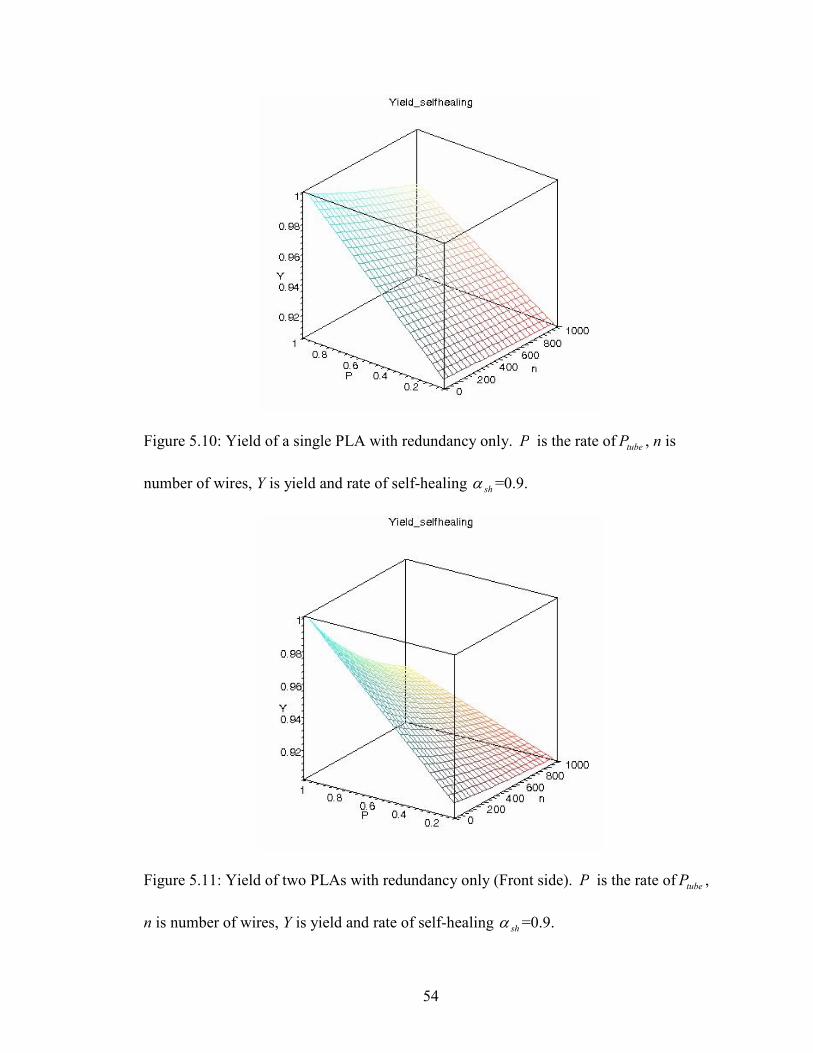
The simulation results for yield with redundancy only and that with self-healing are
shown in Figure 5.1 through Figure 5.12. In the yield with redundancy only model, we
compare between a single PLA yield and extended (two) PLAs yield to know the yield
difference and relation. In order to demonstrate the self-healing capability, we change the
rate of self-healing, shα from 0.5 to 0.9. The rate of tubeP is ranging from 0.1 to 1.0, and a
parameter n, the number of nanowires is ranging from 0 to 1000. Figure 5.1 shows the
yield of a single PLA with redundancy only, shα = 0. In Figure 5.1, the yield of a single
PLA is highest when the yield of nanowire, tubeP is 1.0 and the number of nanowire, n is
small. As tubeP is decreasing and n is increasing, the yield of PLA is decreasing. Figure
5.2 and Figure 5.3 show the yield of two PLAs with redundancy only, and shα is 0 from
different angle. Figure 5.4 shows the yield of a single PLA with self-healing ( shα = 0.5).
In Figure 5.4, the range of yield is from 0.5 to 1.0 because the rates of self-healing
increase the yield of PLA. Figure 5.5 and Figure 5.6 show the yield of two PLAs with
self-healing ( shα = 0.5) from different angle. Figure 5.7 shows the yield of a single PLA
with self-healing ( shα = 0.7). In Figure 5.7, the range of yield is from 0.7 to 1.0 because
the rates of self-healing increase the yield of PLA. Figure 5.8 and Figure 5.9 show the
yield of two PLAs with self-healing ( shα = 0.7) from different angle. Figure 5.10 shows
the yield of a single PLA with self-healing ( shα = 0.9). In Figure 5.7, the range of yield is
from 0.9 to 1.0 because the rates of self-healing increase the yield of PLA. Figure 5.11
and Figure 5.12 show the yield of two PLAs with self-healing from different angle. From

45
those figures, the yield of a single PLA is higher than two PLAs and self-healing
capability can increase its yield.

46
CHAPTER 5
CONCLUSION
This thesis has presented a study on the yield of carbon-nanotube/nanowire array-based
computing systems. The emphasis was given on the novel property of the technology, the
self-healing capability, and its impact on the yield improvement. The motivation of this
thesis work was that no work has adequately addressed the yield issue such that no work
has taken into account the synergistic effect of the defect/failure-tolerance by redundancy
and self-healing that is the most distinguishing and expected merit of the technology; no
work has efficiently and effectively addressed the architectural impact on the yield along
with the yield improvement processes. This thesis has presented an extensive and
comprehensive review of the recent practices of carbon-nanotube/nanowire technology
and an array-based computing architecture built with carbon-nanotube/nanowire
technology. The carbon-nanotube/nanowire array-based computing architecture has been
comprehensively characterized; architecture-specific practical defects and failures have
been extensively characterized and probabilistically parameterized with specific
architectural as well as computational factors taken into account; and the yield of the
system with such architecture has been incrementally developed. Based on the proposed
yield model, parametric simulation has been conducted and it has revealed the synergistic
impact of conventional redundancy-based defect/failure-tolerance and self-healing

47
capability on the yield through comparative study. This thesis work will ultimately
provide a sound theoretical foundation for optimization of carbon-nanotube/nanowire-
based computing systems architecture design and fabrication.

48
Figure 5.1: Yield of a single PLA with redundancy only. P is the rate of tubeP , n is
number of wires, Y is yield and rate of self-healing shα =0.0.
Figure 5.2: Yield of two PLAs with redundancy only (Front side). P is the rate of tubeP , n
is number of wires, Y is yield and rate of self-healing shα =0.0.

49
Figure 5.3: Yield of two PLAs with redundancy only (Back side). P is the rate of tubeP , n
is number of wires, Y is yield and rate of self-healing shα =0.0.

50
Figure 5.4: Yield of a single PLA with redundancy only. P is the rate of tubeP , n is
number of wires, Y is yield and rate of self-healing shα =0.5.
Figure 5.5: Yield of two PLAs with redundancy only (Front side). P is the rate of tubeP , n
is number of wires, Y is yield and rate of self-healing shα =0.5.

51
Figure 5.6: Yield of two PLAs with redundancy only (Back side). P is the rate of tubeP , n
is number of wires, Y is yield and rate of self-healing shα =0.5.

52
Figure 5.7: Yield of a single PLA with redundancy only. P is the rate of tubeP , n is
number of wires, Y is yield and rate of self-healing shα =0.7.
Figure 5.8: Yield of two PLAs with redundancy only (Front side). P is the rate of tubeP , n
is number of wires, Y is yield and rate of self-healing shα =0.7.

53
Figure 5.9: Yield of two PLAs with redundancy only (Back side). P is the rate of tubeP , n
is number of wires, Y is yield and rate of self-healing shα =0.7.
54
Figure 5.10: Yield of a single PLA with redundancy only. P is the rate of tubeP , n is
number of wires, Y is yield and rate of self-healing shα =0.9.
Figure 5.11: Yield of two PLAs with redundancy only (Front side). P is the rate of tubeP ,
n is number of wires, Y is yield and rate of self-healing shα =0.9.

55
Figure 5.12: Yield of two PLAs with redundancy only (Back side). P is the rate of tubeP ,
n is number of wires, Y is yield and rate of self-healing shα =0.9.

56
REFERENCES
[1] Andre Dehon, Array-Based Architecture for FET-based, Nanoscale Electronics, IEEE
Transaction on Nanotechnology, VOL.2, NO. 1, March 2003.
[2] Andre Dehon, Array-Based Architecture for Molecular Electronics, Proceedings of
the First Workshop on Non-Silicon computation, NSC-1, Feb 3, 2002.
[3] Al-Arian, S.A., Gumusel, M.B., HPTR: Hardware partition in time redundancy
technique for fault tolerance, Southeastoncon '92, Proceedings., IEEE, 12-15 April 1992
Pages: 630-633 Vol.2.
[4] Blochl P. E., Stathis J. H, Hydrogen Electrochemistry and Stress-Induced Leakage
Current in Silica, Phys. Rev. Lett. 83 (1991) 372.
[5] Bouricius W. G., Carter W. C., Schneider P.R., Reliability modeling techniques for
self-reparing computer systems, Proceedings of 24th National Conferences, ACM, 1969,
pp. 395-409.
[6] Chen J., Wang W., Reed M. A., Rawlett M., Price D. W., and Tour J. M., Room
temperature Negative Differential Resistance in Nanoscale Molecular Junctions, Appl.
Phys. Lett., vol. 77, pp. 1224, 2000.
[7] Ding-Ming Kwai, Parhami B., Fault-Tolerant Processor Arrays Using Space and
Time Redundancy, Algorithms and Architectures for Parallel Processing, 1996. ICAPP
'96. 1996 IEEE Second International Conference on, 11-13 June 1996 Pages: 303-310.
[8] Dong Qian, Gregory J Wagner, and Wing Kam Liu, Mechanics of carbon nanotubes,
Appl Mech Rev vol 55, no 6, November 2002 Page 3.

57
[9] Huang Y. Duan X., Cui Y., Lauhon L., Kim K-H., and Lieber C., Logic Gates and
Computation from Assembled Nanowire Building Blocks, Science, vol. 294, pp. 1313,
2001.
[10] Huang Y., Duan X., Wei Y., and Lieber C. M., Directed assemble of one-
dimensional nanostructures into functional networks, Science, vol. 300, pp. 112-115, Apr
2003.
[11] Iijima S., Helical Microtubules of Graphitic Carbon, Nature, vol. 354, pp. 56, 1991.
[12] Ion irradiation as a tool for studying and modifying properties of carbo nanotubes,
Simulated STM images of defects in nanotubes,
http://beam.helsinki.fi/nanotubes/stm/stm2.html
[13] Lieber C. M., and Duan X., Nanofet threshold voltages, Dec. 2001.
[14] Michael Butts, Andre Dehon, and Seth Copen Goldstein, Molecular Electronics:
Devices, Systems and Tools for Gigagate, Gigabit Chips, Computer Aided Design, 2002.
ICCAD 2002. IEEE/ADM International Conference on, 10-14 Nov. 2002. pages: 433-
440
[15] Peercy M. and Banerjee P., Fault-tolerant VLSI systems, Proc. IEEE, vol. 81, no 5,
pp. 745-758, May 1993.
[16] Philip Koopman, Elements of the Self-Healing System Problem Space, Institute for
Software Research, International and ECE Department, Carnegie Mellon University.
[17] Rodney S. Ruoff, Dong Qian, Wing Liu, Mechanical properties of carbon
nanotubes: theoretical predictions and experimental measurements, C. R. Physique 4
(2003) 993-1008.

58
[18] Rueckes T., Kim K., Joselevish E., Tseng G. Y., Cheung C. L. and Lieber C. M.,
Carbon nanotubes based nonvolatile random access memory for molecular computing,
Science, vol. 289, pp. 94-97, 2000.
[19] Shamik Das, Garrett Rose, Matthew M. Ziegler, Carl A. Picconatto, and Janmes C.
Ellenbogen, Architectures and Simuations for Nanoprocessor Systems Integrated on the
Molecular Scale, Advances in Molecular Electronics: From molecular materials to single
molecule devices workshop: outlook part chapter 17, February 23 - 27, 2004.
[20] Shanrui Zhang, Minsu Choi, Park N., Modeling yield of carbon-nanotube/silicon-
nanowire FET-based nanoarray achitecture with h-hot addressing scheme, Defect and
Fault Tolerance in VLSI Systems, 2004. DFT 2004 Proceedings. 19th IEEE International
Symposium on, 10-13 Oct. 2004.
[21] Von Neumann, J., Probabilistic logics and the synthesis of reliable organisms from
unreliable components, 1956, in Taub, A. H., (ed.), John von Neumann: collected works,
Volume V, pp. 329-378, New York: Pergamon Press, 1963.
[22] Yokozawa A., Miyamoto Y., Hydrogen dynamics in SiO2 triggered by electronic
excitations, J. Appl. Phys. 88 (2000) 4542.
[23] Yoshiyuki Miyahomoto, Miyamoto Y., Simulation of Ultra-Fast Dynamics in
Carbon Nanotubes Triggered by Illumination, SX WORLD, Autumn 2002 No. 28.
[24] Yoshiyuki Miyamoto, Saves Berber, Mina Yoon, Angel Rubio, and David Tom-
anek, Can photo excitations heal defects in carbon nanotubes?, Chemical Physics
Letters, 2004, v 392, N 1-3, 1 July.

VITA
Jongho Seol
Candidate for the Degree of
Master of Science Thesis: A STUDY ON THE YIELD OF SELF-HEALING CARBON
NANOTUBE/NANOWIRE-BASED SYSTEM Major Field: Computer Science Biographical:
Personal Data: Born in Seoul, Korea, April 6, 1972, son of Hyo-yoon Seol and Hwa-ja Kim.
Education: Graduated from Yoido High School, Seoul, Korea in February 1991.
Received Bachelor of Engineering degree in Computer and Control Engineering from Samcheok National University, Samcheok, Kangwondo, Korea in February 2000. Completed the requirements for the Master of Science degree in Computer Science at the Computer Science Department of Oklahoma State University in May, 2005.
Experience: August, 2003 – May, 2005: Graduate Research Assistant, Computer Science
Department, Oklahoma State University. August, 1993 – October, 1995: Army Service in Seoul, Korea. Professional Memberships: ACM student member in Oklahoma State
University.

Name: Jongho Seol Date of Degree: May, 2005 Institution: Oklahoma State University Location: Stillwater, Oklahoma Title of Study: A STUDY ON THE YIELD OF SELF-HEALING CARBON NANOTUBE/NANOWIRE-BASED SYSTEM Page in Study: 58 Candidate for the Degree of Master of Science Major Field: Computer Science Scope and Method of Study: This thesis is a study on the yield of a digital computing
system built with an emerging technology, carbon-nanotube/nanowire. The emphasis is given on the yield improvement. This thesis presents an extensive and comprehensive review of the recent practices of carbon-nanotube/nanowire technology. The objectives of this thesis are: characterization of a carbon-nanotube/nanowire array-based computing architecture; architecture-based characterization and probabilistic parameterization of practical defects and failures; and incremental modeling and analysis of the yield of the system with such architecture. Based on the proposed yield model, parametric simulation is conducted to reveal the synergistic impact of conventional redundancy-based defect/failure-tolerance and self-healing capability on the yield through comparative study.
Findings and Conclusions: This thesis has presented a study on the yield of carbon-
nanotube/nanowire array-based computing systems. The emphasis was given on the novel property of the technology, the self-healing capability, and its impact on the yield improvement. This thesis has presented an extensive and comprehensive review of the recent practices of carbon-nanotube/nanowire technology and an array-based computing architecture built with carbon-nanotube/nanowire technology. The carbon-nanotube/nanowire array-based computing architecture has been comprehensively characterized; architecture-specific practical defects and failures have been extensively characterized and probabilistically parameterized with specific architectural as well as computational factors taken into account; and the yield of the system with such architecture has been incrementally developed. Based on the proposed yield model, parametric simulation has been conducted and it has revealed the synergistic impact of conventional redundancy-based defect/failure-tolerance and self-healing capability on the yield through comparative study. This thesis work will ultimately provide a sound theoretical foundation for optimization of carbon-nanotube/nanowire-based computing systems architecture design and fabrication.
ADVISOR’S APPROVAL: N. Park