Embed Size (px)
Citation preview
Vacuum/volume 51/number 4/pages 479 to 484/1998© 1998 Published by Elsevier Science Ltd\ Pergamon All rights reserved. Printed in Great Britain
0042–207X/98/$ - see front matterPII: S0042–207X(98)00238–3
A sputter equipment simulation system for VLSIdevice
T. Ohta,* H. Yamada, ULSI Device Development Laboratories, NEC Corporation, 1120 Shimokuzawa,Sagamihara, Kanagawa 229, Japan
In order to optimize the sputter deposition process to fill a minute VLSI’s contact hole efficiently, we havedeveloped a practical sputter equipment simulation system named ‘‘SimDepo’’. The system is composed of(1) the trajectory calculation of sputtered particles using the Monte Carlo method taking into account thecollisions of the sputtered particles with the background gas, (2) the profile calculation using the quasi-axis-symmetrical (QAS) approximation, (3) the ejection angle calculation using molecular dynamic model fortarget atom scattering and (4) the flow calculation considering surface diffusion occurring to minimize thesurface free energy. Using this system, the simulated profiles of collimated sputter titanium (Ti) well agreewith the experimental profiles within 5% accuracy. This system is also applied to the aluminum sputterdeposition process. © 1998 Published by Elsevier Science Ltd. All rights reserved.
Introduction
The sputter technology is used in many industries and especiallyin the semiconductor industry\ the sputter deposition process isgenerally used for fabricating metal wires of VLSI devices[ Asthe integration of VLSI|s increases\ the size of a contact holedecreases[ So\ it has become more di.cult to _ll the minutecontact hole with sputter deposited metals[ Simulation tech!nologies have been developed not only in order to optimize theprocess conditions e.ciently but also to explore the novel sput!tering methods to increase the bottom coverage of contact holes[
Some models for obtaining the particle trajectories in theequipment have been developed using Monte Carlo "MC#method[0\1 Kersch et al[2 utilized the direct simulation MonteCarlo "DSMC# model\ which was applied for the equipmentdevelopment[ Although\ in their calculation\ the equipmentgeometry was approximated with a 1D cylindrical form pre!sumably because of the long simulation time for 2D and for thisreason any pro_les sputter deposited hole was not obtained[Baumann3 developed the MC model with the geometry calcu!lation\ and showed that the calculated pro_les were in agreementwith the experiments[ But the trajectories of particles were cal!culated by the ballistic motion\ so the model was applied to thesimulations only at the low pressure conditions and was notpractically enough for actual sputter process[
The ejection angular distribution of the sputtered particles hasto be considered to evaluate the aspect ratios of contact holes[Concerning the sputtering from the target\ many models have
� Corresponding author[
479
been studied[ The cascade scattering was simulated by using theBoltzmann transport equation or Monte Carlo method[ Someapproaches4 using the molecular dynamic "MD# method werealso developed\ but they left the ejection angle out of consider!ation[
In the case of sputter deposition of aluminum\ the surfacedi}usion of deposited aluminum must be considered[ The alumi!num re~ow pro_les were calculated by the ~uid dynamics codewith the surface melting model[5 It was also shown that thesimulated pro_les well agreed with the experiments[ Surface melt!ing phenomena were proved by the results of simulation with themolecular dynamics "MD#[6 The cluster migration simulated withthe Monte Carlo method7 was also published[ But these cal!culations spent much time and are\ therefore\ impractical foraluminum deposition pro_le simulation[
Our purpose is to develop a practical system being useful forsputter equipment development for manufacturing ULSI[ Forthis purpose\ it is necessary to simulate precise pro_les by con!sidering collisions\ surface di}usion and angular distribution[Reasonable calculation time is also required for the practical use[To solve these subjects\ we have developed a practical sputterequipment simulation system named {{SimDepo||[
In this paper\ we explain the models used in the system andthe system con_guration[ Then we show the results and discussthem[
Models
The models in the simulation systems are selected or developednot only for calculating precise pro_les but also for reducing the
T Ohta and H Yamada: A sputter equipment simulation system for VLSI device
computational time[ Trajectories of sputtered particles in theequipment are calculated using the Monte Carlo method[09 Usingthe obtained trajectories\ sputter deposited pro_les of the contactholes are calculated under the quasi!axis!symmetry "QAS#approximation[09 This system also includes the target atom scat!tering calculation00 considering the molecular dynamics and thecalculation provides the angular distribution of the particles[ The~ow algorithm developed by Leon01 is used for the calculation ofsurface di}usion of aluminum[
Trajectory calculation model[ Figure 0 shows a schematic of asputter apparatus for the trajectory calculation[ Trajectories ofparticles released from a target and collided with background gas"Ar gas# are calculated using the Monte Carlo "MC# method[ Wehave assumed that sputtering rate is so slow and pressure is solow that background gas is approximated uniformly distributed[The simple Monte Carlo method is adopted instead of the {{directsimulation Monte Carlo|| "DSMC# method because the DSMCmethod needs much computational time[
The initial conditions are described as follows] "0# an ejectionposition of a particle is determined from the experimentallyobtained erosion pro_le\ "1# the ejection angular distributionis either derived from cosine low or calculated with the targetscattering model and "2# the particle energy is determined withthe Thompson|s distribution[ The trajectories of the particlesreaching the _xed region on the substrate are extracted and areonly considered in the succeeding calculations[
Collision model[ Background gas is modelled to be distributeduniformly in the chamber[ The distance between the succeedingcollision!positions is determined with the exponential distri!bution[ The velocities of background gas atoms are modelled toobey the Maxwell distribution and calculated using the BoxÐMuller method[
The scattering angle is calculated using the elastic collisionmodel1 taking into account energy dependent collision cross sec!tions[ First\ the relation between the scattered angle "x# and acollision parameter "b#\ derived from the classic dynamics underthe approximation that the colliding particles have LennardÐJones potential taking into consideration the conservation ofenergy and angular momentum\ is numerically solved[ The cal!culated relationship between x and b is linearly approximatedand\ as a result\ the relation between the energy "E# and bmax
"maximum value of b# is tabled[ In the trajectory calculationmodule with the Monte Carlo method\ bmax is derived from the
Figure 0[ A schematic diagram of the MC simulation[ The trajectory ofa particle released from a target and collided with background gas isschematized[
480
obtained table[ Then the collision parameter "b# is calculatedusing a random number ðb�bmax"e0#0:1] e0 is a random numberŁand then the scattering angle is calculated using the linear relationðx�p"0−b:bmax#Ł[ The collision cross section "r# is calculated as]r�pb1
max[
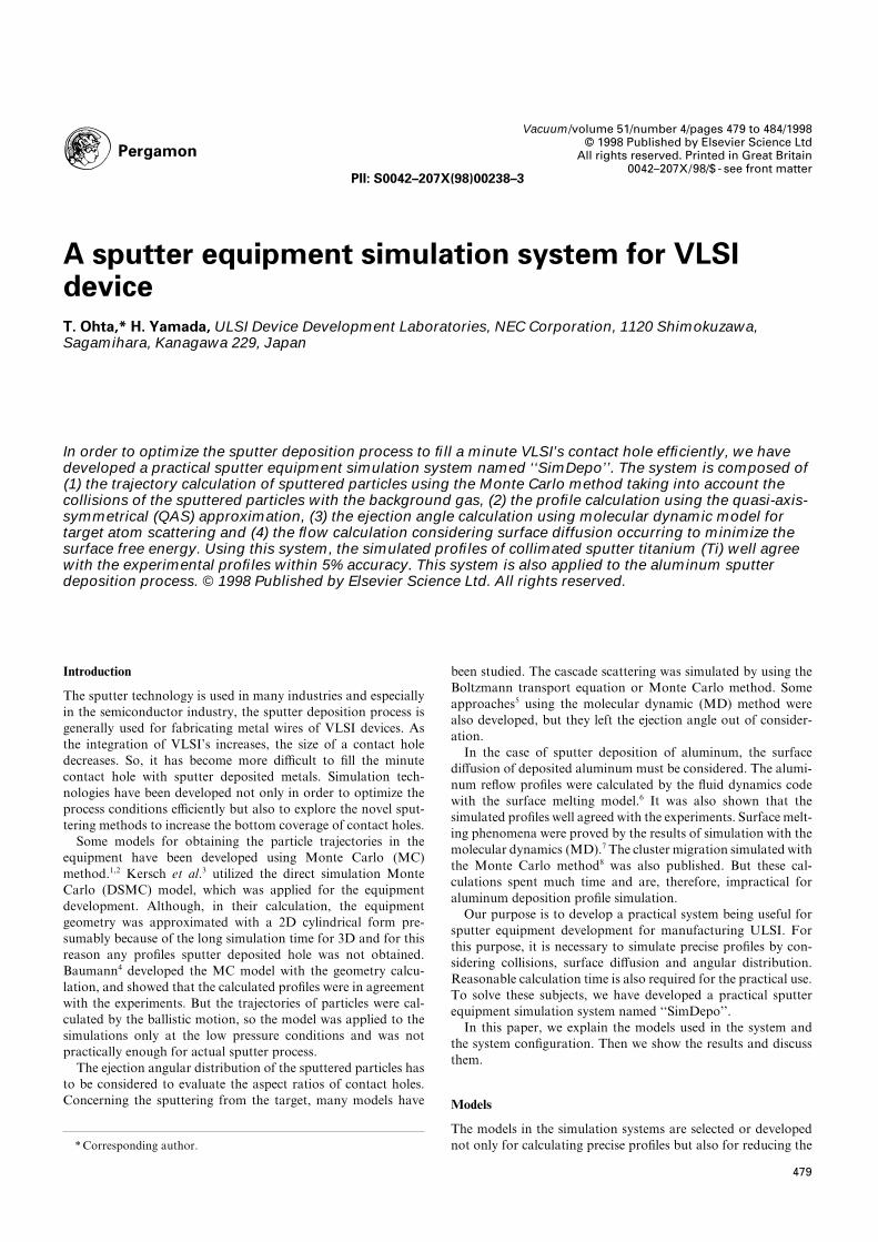
Pro_le calculation model[ Using the trajectories calculated withthe MC method\ the sputter deposition pro_le of a contact holeis calculated under the quasi!axis!symmetrical "QAS# approxi!mation09 with the string model as schematically shown in Fig[ 1[The string points are set in the cross!section of the contact hole[All the trajectories are directed to the string point[ If the distancebetween the cross point of the trajectory with the surface planeand that with the hole axis is larger than the hole radius\ thistrajectory is neglected because of the shadowing and if not thestring point is moved in the cross!section to the next positioncalculated regarding the sticking coe.cient as one[
Surface diffusion model[ In order to simulate the aluminum sput!ter deposition pro_le\ surface di}usion is calculated with the ~owmodel by Leon[01 Surface di}usion is modeled in the follow!ing steps[ The surface chemical potential is derived from thesurface free energy[ Surface di}usion ~ux is derived using Ein!stein|s relation equation[ Considering the mass conservation rule\the pro_le deformed by surface di}usion is calculated with thestring model[
Aluminum pro_les are simulated by repeating both of thedeposition calculation using the trajectories calculated with theMC method and the surface di}usion calculation[ A depositedaluminum pro_le overhanging the contact hole is calculated withthe {{modi_ed|| QAS approximation\8 where the shadow e}ect ofa trajectory is judged for all of the string points[ This approxi!mation needs more computational time but provides more preciseresults than the QAS approximation does[
Target atom scattering model[ The angular distribution of ejectedatoms from a target is calculated using the target atom scatteringmodel described as follows] "0# the ion motion entering into thetarget is calculated with the electric _eld in plasma discharge[ "1#The initial atom velocity distribution in the target is thought to
Figure 1[ A schematic diagram of the quasi!axis!symmetrical "QAS#approximation[ The axis!symmetrical {{shadowing|| and moving directionof the string points are schematized[

T Ohta and H Yamada: A sputter equipment simulation system for VLSI device
Figure[ 2[ Block diagram of sputter simulation system named {{SimDepo||[
be Maxwell distribution with the target surface temperature dur!ing the sputtering\ which is calculated by the thermal analysis[00
"2# The atom motion in the target is calculated with the moleculardynamic technique[ The Newtonian equations under the inter!atomic potentials are numerically solved using velocity Verletmethod[02 For TiÐTi interaction\ the Morse pair potentials areused[ For TiAr interaction\ the universal potential of Ziegler isused[
System composition
In order to simulate and estimate the sputter deposition processand to compare the simulated results and the experimental resultmore easily\ we developed the system with some utilities such asoptimization and graphical user interface "GUI#[
The block diagram of the system named {{SimDepo|| is shownin Fig[ 2[ The system is composed of the modules correspondingwith the models as stated above[ These modules can be executedindividually through the intermediate _les\ which result inimprovement of system performance[ For this purpose in theparticle trajectory calculation module\ the ejection angle of theparticle is determined using the {{rejection method|| from thetable of the ejection angular distribution calculated with thetarget atom scattering model[
In the optimization module\ the target erosion distribution isreversely calculated using linear programming method to max!imize the bottom coverage in the condition of keeping thicknessvariation in the wafer less than 4)[
The system is operated with a graphical user interface "GUI#shown in Fig[ 3[ Motif is adopted as the con_guration of theGUI\ which has made the system easy to be operated[ Using thissystem\ sputter pro_les can be easily simulated for comparing theexperimental results[
Results and discussion
Pro_les of titanium "Ti#[ Simulated pro_les of deposited Ti usingthe collimated!sputter equipment are compared with the exper!imental pro_les[ In the trajectory calculation module\ cosine lowis used for the ejection angular distribution[ Figure 4"a# showsan experimental SEM pro_le at the wafer center of a contact holeusing a 0]0 collimator at a pressure of 9[43 Pa and a substratetemperature of 562 K[ As shown in Fig[ 4"b#\ the simulated pro_lewell agrees with the pro_le obtained from the experiment within4) accuracy[
Figure 5 shows the relation of the Ti bottom coverage to theargon "Ar# pressure[ The simulated bottom coverage well agrees
481
Figure 3[ An example of graphical user interface "GUI# layout[ Motif isadopted as the GUI con_guration[
with the experiments within 4) accuracy at the pressures from9[0 to 0[9 Pa[ The di}erence between the simulation and theexperiment above 0[9 Pa is presumably because of the in~uenceof the viscous ~ow "Knudsen number is lower than 9[0 above0[9 Pa#[
In the trajectory calculation module\ the calculation time forone equipment condition is 029 min using EWS "029MIPS#[ Andthe Ti pro_le calculation time of a contact hole is less than 0 min[
The particle trajectories are calculated with the simple MonteCarlo "MC# method\ instead of the direct simulation MonteCarlo "DSMC# method[ Calculation time with the DSMCmethod is estimated about 19 times as long as the simple MCmethod[ The results show that the simple Monte Carlo methodis suitable for the sputter pro_le simulation in the practical con!dition of Ti sputtering process in spite of the short calculationtime needed[
Aluminum pro_les[ The surface di}usion coe.cients of aluminumnecessary for the simulations are adjusted using experimentalresults[ Figure 6"a# shows an experimental SEM pro_le of acontact hole _lled with aluminum and Fig[ 6"b# shows a simulatedpro_le "after adjustment of the surface di}usion coe.cient# andFig[ 6"c# shows a calculated pro_le leaving the surface di}usionmodel out of consideration[ The surface di}usion considerationis found to be indispensable for aluminum pro_le simulation[The adjusted surface di}usion coe.cients are plotted with the

T Ohta and H Yamada: A sputter equipment simulation system for VLSI device
Figure 4[ "a# SEM photograph of 0[10 aspect ratios contact hole _lled with 1789 A� Ti is deposited at 9[43 Pa and 562 K[ "b# A corresponding simulatedpro_le[
Figure 5[ Simulated bottom coverage and experimental one[
Figure 6[ Simulated aluminum pro_le and experiment[
482

T Ohta and H Yamada: A sputter equipment simulation system for VLSI device
temperatures in Fig[ 7[ The activation energy of the surfacedi}usion is found about 9[02 eV from Fig[ 7[
The calculation time of an aluminum pro_le is about 19 minusing EWS "029MIPS#\ which is much faster than the time bythe ~uid dynamics code with the surface melting model[5 Theactivation energy of surface di}usion coe.cients of aluminum isabout a quarter of the value shown in the previous paper7 "whichis 9[49 eV#[ The surface di}usion coe.cient is about one millionas large as the that of bulk03 at 462 K\ which shows the validityof the assumption that bulk di}usion is negligible[ The result issimilar to the previous paper by Fujinaga et al[04 concerningBPSG "borophosphosilicate glass# re~ow at 749 K[
Pro_les with target scattering model[ Figure 8 shows the three!dimensional "2D# simulation results of ejection angular dis!tribution with the target scattering model of Ti atoms of a "092#surface of a single crystal target with 239 and 509 eV Ar ionbombardments[ The Ti atoms ejected by 509 eV bombardmentare more vertically directional than those in the case of 239 eV
Figure 7[ Arrhenius plot] the adjusted surface di}usion coe.cient vs thetemperature[
Figure 8[ Simulated ejection angle distributions with 239 and 509 eVargon ion bombardments[
483
Figure 09[ Bottom coverages vs aspect ratios of Ti[ The simulated ejectionangle distribution is used[
bombardment[ Figure 09 shows simulated and experimentalresults of the bottom coverage vs aspect ratios of contact holes[The simulated bottom coverage agrees with the experimentalresults within 09) accuracy[
The calculation time of angular distribution of a target is about09 h with EWS "029MIPS#[ The calculation time is thought to bewithin the range of practical use because in the simulation systemthe angular distribution can be calculated independently of theother modules such as the trajectory calculation module[
The target scattering model is e}ective in investigating theway to increase the bottom coverage and\ for example\ we haveinvestigated the angular distribution dependence on the targetsurface orientation[00 The angular distribution of the ejectedatoms from the polycrystalline target can be approximated withthe conventional cosine law because it agrees with the sum ofvarious simulated angular distributions of the single!crystal[
Conclusion
We have developed a practical sputter equipment simulationsystem[ Simulated sputter titanium "Ti# pro_les well agree withthe experimental pro_les within 4) accuracy[ By means of thesurface di}usion model this system is also applied to the alumi!num sputter deposition process[ These results show that the sys!tem can be utilized not only for the optimization of processparameters but also for the apparatus development[
Acknowledgements
The authors would like to thank Mr T[ Shinniura\ Mr Y[ Yamadaand Mr H[ Kaneko for their helpful support and usefuldiscussions[
References
0[ Motohiro\ T[\ J[ Vac[ Sci[ Technol[ A\ 0875\ 3"1#\ 078[1[ Turner\ G[M[\ Falconer\ I[S[\ James\ B[W[ and McKenzie\ D[R[\ J[
Appl[ Phys[\ 0878 54"8#\ 2560[2[ Kersch\ A[\ Moroko}\ W[\ Werner\ C[\ Restanio\ D[ and Vollmer\
B[\ IEDM Tech[ Di`[\ 0881\ 9\ 070[3[ Baumann\ F[B[\ Liu\ R[\ Case\ C[B[ and Lai\ W[Y[!C[\ IEDM Tech[
Di`[\ 0882\ 9\ 750[4[ Valkealabli\ S[ and Nieminen\ R[M[\ Nucl[ Instrum[ Methods B\ 0876\
07\ 254[

T Ohta and H Yamada: A sputter equipment simulation system for VLSI device
5[ Hirose\ K[\ Kikuta\ K[ and Yoshida\ T[\ IEDM Tech[ Di`[\ 0883\ 9\446[
6[ Tsukamoto\ S[\ Iijima\ T[\ Yokozawa\ A[ and Ishitani\ A[\ Conf[Proc[ ULSI I\ 0885\ p[ 108[
7[ Baumann\ F[B[ and Gilmer\ G[H[\ IEDM Tech[ Di`[\ 0884\ 9\ 78[8[ Yamada\ H[\ Ohta\ T[\ Kaneko\ H[ and Yamada\ Y[\ SISPAD|85
Tech[ Dig[\ 0875\ 4!2\ 66[09[ Yamada\ H[\ Shimmura\ M[\ Yamada\ Y[ and Olita\ T[\ IEDM Tech[
Di`[\ 0883\ 9\ 442[
484
00[ Yamada\ H[\ Shimmura\ T[ and Olita\ T[\ IEDM Tech[ Di`[\ 0884\9\ 82[
01[ Leon\ E[A[\ IEEE Trans[ CAD\ 0877\ 6"1#\ 057[02[ Verlet\ L[\ Phys[ Rev[\ 0856\ 048\ 87[03[ Chronological Table of Science\ ed[ Japan National Astronomical
Observatory[ 0883\ p[ 349[04[ Fujinaga\ M[\ Tottori\ L[\ Kunikio\ T[\ Uchida\ T[\ Kotani\ K[ and
Akasaka\ Y[\ SDM!80!090[ 0880\ p[ 12 "in Japanese#[