Embed Size (px)
Citation preview
A Reconfigurable Digital Signal Processing System for Eddy Currents Non-Destructive Testing
Luís S. Rosado
Instituto Superior Técnico, UTL, Lisbon, Portugal, [email protected]
Abstract - This paper presents a digital signal processing system specially designed for eddy currents non-destructive testing. This new system has a Field Programmable Gate Array based processing core, several communication interfaces, data conversion and analog devices to interface the probes. Communication with personal computers is ensured by Ethernet 10/100 and USB 2.0 High Speed interfaces. The proposed architecture enables to set several combinations of peripherals cards to generate or acquire probe signals. Also, the new system allows the digital generation and analysis of the probe signals through multiple digital signal processing algorithms.
Two different peripheral cards have been developed to meet the needs for the new IOnic concept of eddy currents probe. The IOnic acquisition card is composed by a programmable gain amplifier and a high speed analog to digital converter. The current stimulus generation is achieved with a digital to analog converter and a high output current transconductance amplifier. Together, the two peripherals are able to operate the probe from 10 kHz up to 10 MHz. An additional peripheral card to interface stepper motors was designed and used for sensor positioning. Keywords - Non-Destructive Testing; Eddy Currents; Digital Signal Processing; FPGA.
I - INTRODUCTION
From the several Non-Destructive Testing (NDT) methods, eddy currents evaluation is the preferred to inspect metallic parts and welding joints searching for flaws and other material discontinuities. Eddy currents NDT is based on electromagnetic induction and analysis of electrical currents on conductive materials. The principal advantages of using this technology are that surface preparation is minimal and it is a quite intuitive method, setting aside the need for highly qualified personnel.
Typically, eddy currents NDT is performed using a single carrier frequency. However, new stimulus are being adopted such as pulsed eddy currents (PEC), where a broadband pulse is applied as stimuli and the transient response is analyzed. This transient response contains frequency-rich information that is used to infer about the inspection material properties. The potential on using PEC has been demonstrated in [1] where this technique was used to detect defects with several geometrical orientations. Multi-frequency eddy currents (MEC) testing is based on the simultaneous employment of multiple frequency carriers. In [2], the use of this technique demonstrated good results not only for defect detection but also for their characterization.
DSP techniques are been applied to extract the magnetic field information from raw voltage data. In [3] a digital signal processing algorithm was used to improve the overall NDT system performance. The use of digital signal processing techniques can reduce the complexity of NDT systems and, at the same time enlarge their flexibility and therefore their application field. As an example, using the same digital signal processing system, it is possible to implement not only PEC and MEC methods but also a multitude of stimulus patterns and analysis algorithms.
Recently, a new concept of eddy currents probe has been presented [4]. This new IOnic probe demonstrates several advantages over the conventional eddy currents probes and exhibited encouraging results when employed to micro size defects [5]. To extract their maximum performance and expand their application field, a custom digital signal processing system was developed. This innovative system was made highly reconfigurable through the use of programmable logic devices and an architecture that enables the selection between several combinations of cards to generate or acquire probe signals.
II - SYSTEM ARCHITECTURE
The proposed system is an integrated solution for eddy currents signal generation, processing and analysis composed by a digital signal processing electronic system and dedicated NDT software. This solution was made reconfigurable through the use of a FPGA based processing core and the possibility to configure the number and type of peripherals used to generate or acquire the probe stimulus. Also, several communication interfaces have been added providing easy connectivity with personal computers and networks. These communication interfaces can be used to specify acquisition parameters, and exchange pre-processed data. Already in the computer, the pre-processed data can be presented and subject to post-processing features. The overall architecture of the purposed system is presented in Figure 1.
Figure 1 - Purposed system overview.
The FPGA processing core, the communication interfaces and seven socket connectors for peripherals are included on
the main board of the system. Beyond this base hardware, the main board has non-volatile FLASH memory, used to store
software and internal settings, several clock sources and configuration interfaces.
Three different types of peripherals have been designed for signal generation, signal acquisition and controlling the stepper motors of the positioning system. The functional diagram of the processing core is illustrated in Figure 2. The peripheral card responsible for the probe input current generation is composed by a 14 bits Digital to Analog Converter (DAC) followed by probe driver circuit featuring high output current and an extended frequency operation range. Signal acquisition is achieved with a 14 bits high speed Analog to Digital Converter (ADC) connected to a Programmable Gain Amplifier (PGA) where the input signal amplification is controlled by a four bits gain digital code. An additional peripheral was designed to simultaneous control up to three axis on a XY Table used for sensor positioning.
Figure 2 - Main Board functional diagram.
III - FPGA BASED PROCESSING CORE
FPGAs have some advantages for digital signal processing when compared to DSP processors. The performance of FPGAs results from the ability to build highly parallel processing structures. Unlike DSP processors, where performance is tied to the clock frequency and the Arithmetic Logic Unit efficiency, FPGA performance is related with the amount of parallelism that can be achieved in a certain algorithm. The increasing speed, high flexibility and performance make FPGAs ideal for high data rate digital signal processing. The main device of the purposed system is a XC3SD3400A FPGA specially tailored for memory-intensive, digital signal processing cost-sensitive applications. To meet this objective, this device has about 2 Mbits of integrated RAM and 126 DSP48A slices. DSP48A slices perform high speed multiply and accumulate operations for 18x18 two’s complement operands at 250 MHz, being particularly useful
on building digital signal processing structures. The main features of XC3SD3400A device are listed in Table 1.
Table 1 - XC3SD3400A-4CSG484C Features.
Array (RowxCol)
System Gates
Spartan-3®
Slices DSP48A
Slices BRAM (Kbit)
User IO
104x58 3400 K 23872 126 2268 309
An Atmel AT45DB Serial Peripheral Interface (SPI) Flash
device provides 32 Mbits of non-volatile memory for storing the embedded application. This device can be configured using Parallel IV programmers and XILINX proprietary tools.
All the supply voltages needed are obtained with step-down switching converters PTH05050 and the system is powered by ATX compliant power supply.
USB communications are ensured by a CY7C68013A integrated controller. This chip makes use of Cypress FX2 technology and is a highly integrated, low power USB 2.0 High Speed microcontroller. CY7C68013A contains on the same package a transceiver, a serial-parallel conversion mechanism, several programmable interfaces and an enhanced 8051 microcontroller. All the configuration tasks are done by firmware and executed by the 8051 microcontroller while the high speed data processing is handled in hardware. The various interfaces and an architecture that enables multiple operation modes configurable by firmware make the FX2 a quite versatile solution. The internal Smart USB Engine controls almost all the USB protocol tasks in hardware reducing the development time needed to achieve full compatibility. The FPGA communicates with the USB controller through eight 512 byte memory blocks that are configured as a First In First Out (FIFO) queue to send and receive data from the USB.
The Ethernet interface is based on the National Semiconductor DP83865 Physical Layer Transceiver. The upper layers of the communication protocol are implemented inside the FPGA using both dedicated hardware and software. National Semiconductor DP83848TSQ communicates with the logic inside the FPGA through a Media Independent Interface (MII). The MII transfers data using 4-bit words in each direction, clocked at 25 MHz to achieve a maximum of 100 Mbit/s speed.
IV - PERIPHERAL CARDS
Peripheral cards are responsible for interfacing with the probes and to control the stepper motors of the motion and positioning system. All the peripherals cards were designed to fit the socket connectors in the main board. To ensure the compatibility between the main board connector and the three different card types, a common pinout structure to be shared between the cards was defined.
A. IOnic Driver Card
This card is composed by a DAC and a probe driver circuit. The DAC performs the conversion of the digital stimulus processed in the FPGA to a voltage signal that is converted to the probe current in the probe driver circuit.
AD9707 performs digital to analog conversion at rates up to 175 MS/s. This converter has excellent dynamic linearity

and relatively low power consumption when powered with 3.3 V. Furthermore, their internal temperature compensated reference is used to set the full scale output current minimizing external components. The sampling clock is transmitted in Low Voltage Differential Signaling (LVDS) and the input 14 bits digital word is expressed in offset binary format.
The probe driver circuit is a high output current transconductance amplifier that is attached to the digital to analog converter. This amplifier is composed by an input stage AD8000 High performance OPAMP and an output stage with power MOSFETs. The output stage transistors are wired on a source follower configuration and can operate in both class A and AB in order to achieve low distortion or low power consumption. The simplified schematic for the probe driver circuit can be seen in Figure 4. On this configuration, the DC feedback through components 1 and 2 sets the steady state voltage level on the output stage to the middle of the supply voltage. Capacitor 3 blocks the load DC component allowing that only AC current flows in the driver trace. The AC feedback is done in the sense resistor 6 and the gain is set by
5 and 2. Hence, the transconductance gain for the driver circuit is
1 (1)
Figure 3 - Probe driver circuit.
The frequency response of the circuit was measured using
an Agilent 4395A with about 55 mV input amplitude corresponding to a 1 A amplitude output current. The obtained transconductance gain profile is represented in Figure 5. The -3dB low cut-off frequency is 1 kHz and 14 MHz for the high pass cut-off frequency.
Figure 4 - Probe driver circuit frequency response.
To evaluate the distortion of the generated current signals,
the response of the driver circuit was analyzed. Making use of a Agilent 54622A 250 MSPS oscilloscope measuring the voltage across 6 and a TTi TG1010A function generator, 2
million points sequences were acquired for 10 kHz, 100 kHz, 1 MHz and 10 MHz and 1 A sine waves output currents. These sequences were processed by the Matlab DFT algorithm and the Total Harmonic Distortion (THD) was calculated. Figure 6 shows the time domain signal for the 10 MHz sine wave output current and their frequency domain representation.
Figure 5 - Probe driver circuit transient response and corresponding frequency domain representation for 1 A amplitude, 10 MHz frequency sine wave output
current.
The THD values for the four analyzed frequencies are
described in Table 2 together with the generator THD extracted from their datasheet [6]. The circuit seems to introduce very low distortion as the measured THD is close to the maximum THD announced by the generator manufacturer.
Table 2 - Probe Driver circuit THD.
Frequency Measured THD [dB] TG1010A THD [dB]
10 kHz - 51.11 < - 60
100 kHz - 51.06 < -60
1 MHz - 58.20 < -50
10 MHz - 31.83 < -35
B. IOnic Acquisition Card
The acquisition card is composed by a programmable gain amplifier and an analog to digital converter. The programmable gain amplifier is used to extend the dynamic range of the ADC which converts the amplified signals to be processed in the FPGA.
The analog to digital conversion is achieved by the AD9246 Analog to Digital Converter with 14 bit resolution. There are three commercial versions of the circuit with different maximum sampling rates of 80, 105 and 125 MSPS. In the 125 MSPS version, this converter consumes only 395 mW when powered with a 1.8 V source. Furthermore, the output data register can be configured to generate offset binary, gray code or two’s complement codes. The AD9246 features outstanding dynamic specifications achieving an Effective Number of Bits of 11.7 when converting a 10 MHz sine wave.
To extend the input dynamic range, an amplification chain composed by a 20 dB pre-amplifier and a 40 dB maximum digital controlled amplifier was designed. The pre-amplification is achieved with the low noise amplifier
AD8351. Controlled gain is implemented with AD8369 and on 3 dB steps from -5 dB to 40 dB maximum with 4 digital input signals. Unlike conventional programmable gain amplifiers, the AD8369 operation is based on controlling the transconductance of the output stage. In this architecture, the 3 dB cut-off frequency remains independent from the selected gain. Once again, using the Agilent 4395A, the frequency response of the amplification chain was characterized. The frequency response for the gain codes in Table 3 has been registered in Figure 9.
Table 3 - Gain codes and overall gain.
Gain Code AD8369 Gain [dB] Overall Gain [dB]
0001 - 2 18
0010 1 21
0100 7 27
1000 19 39
1111 40 60
Figure 6 - Programmable gain amplifier frequency response.
Time and frequency analysis was done using the same equipment and frequencies as the driver circuit. Figure 8 shows the time domain signal for the programmable gain amplifier output when the input is a 10 MHz, 5 mV amplitude sine wave and the gain code is set to 1000 (39 dB overall gain). On the same figure the frequency domain representation of the output signal is presented.
Figure 7 - Programmable gain amplifier transient response and corresponding frequency domain representation for 5 mV amplitude, 10 MHz frequency sine
wave input voltage.
A. Positioning Control Card To enable the control of the positioning system, an
additional peripheral card was designed. This peripheral has stepper motors control devices for three different axes. L297 together with L298 integrated circuits are used to control and drive a wide range of stepper motors and provide a simple communication interface of only 5 signals per axis.
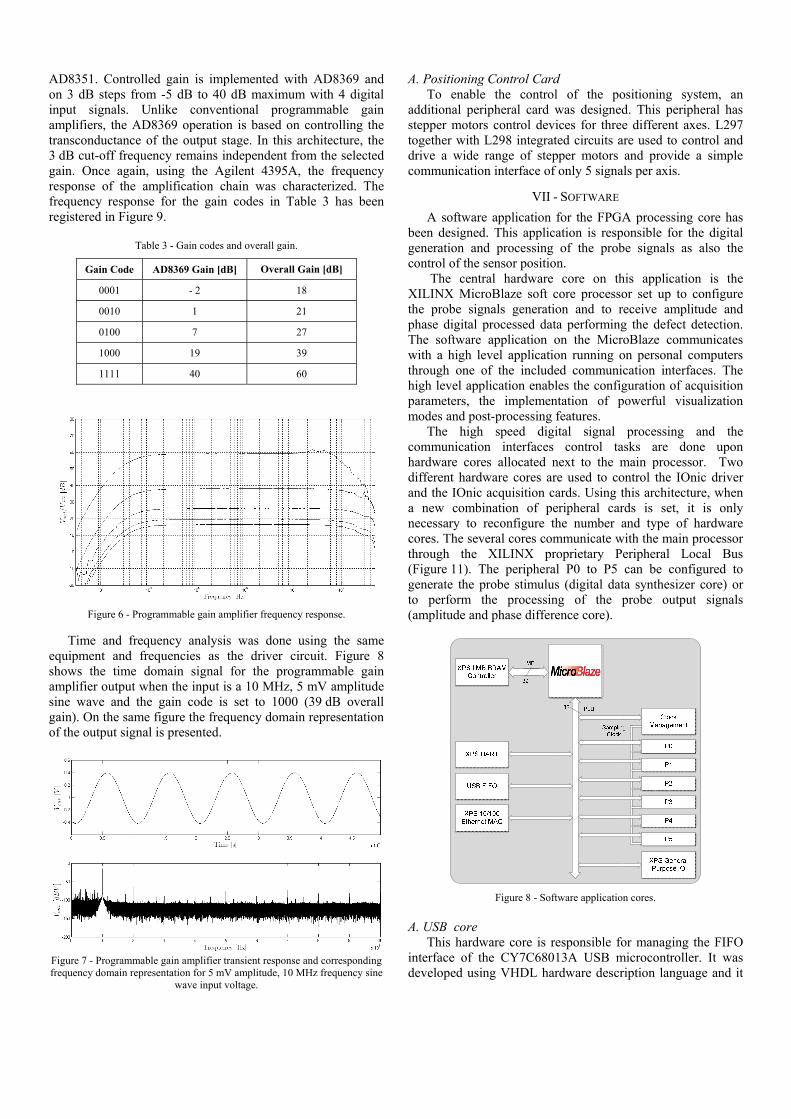
VII - SOFTWARE
A software application for the FPGA processing core has been designed. This application is responsible for the digital generation and processing of the probe signals as also the control of the sensor position.
The central hardware core on this application is the XILINX MicroBlaze soft core processor set up to configure the probe signals generation and to receive amplitude and phase digital processed data performing the defect detection. The software application on the MicroBlaze communicates with a high level application running on personal computers through one of the included communication interfaces. The high level application enables the configuration of acquisition parameters, the implementation of powerful visualization modes and post-processing features.
The high speed digital signal processing and the communication interfaces control tasks are done upon hardware cores allocated next to the main processor. Two different hardware cores are used to control the IOnic driver and the IOnic acquisition cards. Using this architecture, when a new combination of peripheral cards is set, it is only necessary to reconfigure the number and type of hardware cores. The several cores communicate with the main processor through the XILINX proprietary Peripheral Local Bus (Figure 11). The peripheral P0 to P5 can be configured to generate the probe stimulus (digital data synthesizer core) or to perform the processing of the probe output signals (amplitude and phase difference core).
Figure 8 - Software application cores.
A. USB core
This hardware core is responsible for managing the FIFO interface of the CY7C68013A USB microcontroller. It was developed using VHDL hardware description language and it

consists of a finite state machine controlled by internal registers that can be accessed through the PLB bus.
B. Ethernet core
The 10/100 Ethernet MAC Lite XILINX core ensures the communication with the DP83865 Physical Layer Transceiver over the MII interface. The management of the TCP/IP protocol is done using the LightWeight IP Stack library.
C. Digital Data Synthesizer core
The digital data synthesizer generates the digital stimulus to be converted in the IOnic driver card. The developed synthesizer is composed by a numerically controlled oscillator, a sine wave look-up table and additional logic to control the amplitude and the phase delay.
D. Amplitude and phase difference core
The amplitude and phase difference demodulator is still being developed. In the final structure, the phase detection should be done with a XOR logical function and an IIR low pass filter. The amplitude detection will be achieved by estimating the sine wave RMS value.
VIII - CONCLUSIONS
A new eddy currents non-destructive testing system enabled for high speed digital signal processing was presented. The architecture allows the reconfiguration not only of the algorithms to be implemented but also of the number and type of peripherals for interfacing with the probes. Analog
electronics to interface the new IOnic eddy currents probe was described and characterized. The new probe front-end seems to be able to work properly on frequencies up to 10 MHz exhibiting excellent dynamic characteristics.
Software for communications, signal generation and processing has been developed. The purposed software architecture makes use of hardware cores to handle the high speed data processing and communication tasks and a soft-core processor to control the probe acquisition parameters and to communicate with an high level application running in a personal computer.
REFERENCES [1] L. Shu, H. Songling, Z. Wei, Y. Peng, “Study of pulse eddy current
probes detecting cracks extending in all directions”, Sensors and Actuators A, no. 141, pp. 13-19, 2008.
[2] T. Chady, M. Enokizono, "Multi-frequency exciting and spectrogram-based ECT method”, Journal of Magnetism and Magnetic Materials vol. 215-216, pp. 700-703, 2000.
[3] A. Bernieri, G. Betta, L. Ferrigno, “Improving Nondestructive Testing Probe Performance by Digital Processing Techniques”, IEEE Transactions on Instrumentation and Measurement, vol. 52, no. 3, June 2003.
[4] Portuguese Patent N.º PT 104089 – Método de Ensaio Não Destrutivo Baseado em Variante de Sonda de Correntes induzidas, Inventors: Telmo Santos, Moisés Piedade, Pedro Vilaça, June, 2008 (in portuguese).
[5] L. Rosado, T. Santos, M. Piedade, P. M. Ramos, P. Vilaça, “New Non Destructive Test Technique on Metal inspection”, XIX IMEKO World Congress, Lisbon, Portugal, September 2009.
[6] TTi TG1010A Data Sheet (in TTi), ref: 82100-0057 Issue 2.