Embed Size (px)
Citation preview
A photonic analog-to-digital converter using phase modulation and self-coherent detection
with spatial oversampling Ori Golani,1,* Luca Mauri,2 Fabiano Pasinato,2 Cristian Cattaneo,2 Guido Consonnni,2
Stefano Balsamo,2 and Dan M. Marom1 1Department of applied physics, Hebrew University, Jerusalem Israel
2Oclaro Corporation, San Donato, Italy *[email protected]
Abstract: We propose a new type of photonic analog-to-digital converter (ADC), designed for high-resolution (>7 bit) and high sampling rates (scalable to tens of GS/s). It is based on encoding the input analog voltage signal onto the phase of an optical pulse stream originating from a mode-locked laser, and uses spatial oversampling as a means to improve the conversion resolution. This paper describes the concept of spatial oversampling and draws its similarities to the commonly used temporal oversampling. The design and fabrication of a LiNbO3/silica hybrid photonic integrated circuit for implementing the spatial oversampling is shown, and its abilities are demonstrated experimentally by digitizing gigahertz signals (frequencies up to 18GHz) at an undersampled rate of 2.56GS/s with a conversion resolution of up to 7.6 effective bits. Oversampling factors of 1-4 are demonstrated.
©2014 Optical Society of America
OCIS codes: (060.5625) Radio frequency photonics; (070.1170) Analog optical signal processing; (320.7085) Ultrafast information processing.
References and links 1. R. H. Walden, “Analog-to-digital converter survey and analysis,” IEEE J. Sel. Areas Comm. 17(4), 539–550
(1999). 2. A. Bartels, S. A. Diddams, T. M. Ramond, and L. Hollberg, “Mode-locked laser pulse trains with
subfemtosecond timing jitter synchronized to an optical reference oscillator,” Opt. Lett. 28(8), 663–665 (2003). 3. G. C. Valley, “Photonic analog-to-digital converters,” Opt. Express 15(5), 1955–1982 (2007). 4. A. O. J. Wiberg, L. Liu, Z. Tong, E. Myslivets, V. Ataie, B. P.-P. Kuo, N. Alic, and S. Radic, “Photonic
preprocessor for analog-to-digital-converter using a cavity-less pulse source,” Opt. Express 20(26), B419–B427 (2012).
5. A. O. J. Wiberg, D. J. Esman, L. Liu, Z. I. Tong, E. Myslivets, N. Alic, and S. Radic, “Demonstration of 74 GHz parametric optical sampled analog-to-digital conversion,” Optical Communication (ECOC 2013).
6. T. Satoh, K. Takahashi, H. Matsui, K. Itoh, and T. Konishi, “10-GS/s 5-bit Real-Time Optical Quantization for Photonic Analog-to-Digital Conversion,” IEEE Photon. Technol. Lett. 24(10), 830–832 (2012).
7. C. Xu and X. Liu, “Photonic analog-to-digital converter using soliton self-frequency shift and interleaving spectral filters,” Opt. Lett. 28(12), 986–988 (2003).
8. J. Stigwall and S. Galt, “Demonstration and Analysis of a 40-Gigasample/s Interferometric Analog-to-Digital Converter,” J. Lightwave Technol. 24(3), 1247–1256 (2006).
9. M. Jarrahi, R. F. W. Pease, D. A. B. Miller, and T. H. Lee, “Optical Spatial Quantization for Higher Performance Analog-to-Digital Conversion,” IEEE Trans. Microw. Theory Tech. 56(9), 2143–2150 (2008).
10. W. Li, H. Zhang, Q. Wu, Z. Zhang, and M. Yao, “All-Optical Analog-to-Digital Conversion Based on Polarization-Differential Interference and Phase Modulation,” IEEE Photon. Technol. Lett. 19(8), 625–627 (2007).
11. A. J. Price, R. Zanoni, and P. J. Morgan, “Photonic analog-to-digital converter,” US Patent No. 7876246 B1, (2011).
12. T. D. Gathman and J. F. Buckwalter, “An 8-bit Integrate-and-Sample Receiver for Rate-Scalable Photonic Analog-to-Digital Conversion,” IEEE Trans. Microw. Theory Tech. 60(12), 3798–3809 (2012).
13. A. Khilo, S. J. Spector, M. E. Grein, A. H. Nejadmalayeri, C. W. Holzwarth, M. Y. Sander, M. S. Dahlem, M. Y. Peng, M. W. Geis, N. A. DiLello, J. U. Yoon, A. Motamedi, J. S. Orcutt, J. P. Wang, C. M. Sorace-Agaskar, M. A. Popović, J. Sun, G.-R. Zhou, H. Byun, J. Chen, J. L. Hoyt, H. I. Smith, R. J. Ram, M. Perrott, T. M.
#208458 - $15.00 USD Received 17 Mar 2014; revised 30 Apr 2014; accepted 30 Apr 2014; published 13 May 2014(C) 2014 OSA 19 May 2014 | Vol. 22, No. 10 | DOI:10.1364/OE.22.012273 | OPTICS EXPRESS 12273
Lyszczarz, E. P. Ippen, and F. X. Kärtner, “Photonic ADC: overcoming the bottleneck of electronic jitter,” Opt. Express 20(4), 4454–4469 (2012).
14. D. R. Reilly, S. X. Wang, and G. S. Kanter, “Optical under-sampling for high resolution analog-to-digital conversion,” in Proceedings of Avionics, Fiber- Optics and Photonics Technology Conference (AVFOP), 35–36 (2011).
15. D. Sinefeld, Y. Fattal, and D. M. Marom, “Generation of WDM adaptive-rate pulse bursts by cascading narrow/wideband tunable optical dispersion compensators,” Opt. Lett. 37(20), 4290–4292 (2012).
16. D. Sinefeld, D. Shayovitz, O. Golani, and D. M. Marom, “Tunable WDM Sampling Pulse Streams using a Spatial Phase Modulator in a Biased Pulse Shaper,” Opt. Lett. 39(3), 642–645 (2014).
17. J. van Howe, J. Hansryd, and C. Xu, “Multiwavelength pulse generator using time-lens compression,” Opt. Lett. 29(13), 1470–1472 (2004).
18. H. Q. Lam, K. E. K. Lee, and P. H. Lim, “Time- and wavelength-interleaved optical pulse train generation based on dispersion spreading and sectional compression,” Opt. Lett. 37(12), 2349–2351 (2012).
19. J. Vasseur, M. Hanna, J. M. Dudley, and J.-P. Goedgebuer, “Generation of interleaved pulses on time-wavelength grid by actively modelocked fibre laser,” Electron. Lett. 40(14), 901 (2004).
20. H. F. Taylor, “An optical analog-to-digital converter - Design and analysis,” IEEE J. Quantum Electron. 15(4), 210–216 (1979).
21. L. Tan and D. S. Processing, Fundamentals and Applications, (Academic Press. 2008). 22. P. Carbone and D. Petri, “Effect of Additive Dither on the Resolution of Ideal Quantizers,” IEEE Trans. Instrum.
Meas. 43(3), 389–396 (1994). 23. S.-H. Jeong and K. Morito, “Optical 60° hybrid for demodulating six-level DPSK signal,” Opt. Lett. 36(3), 322–
324 (2011). 24. S.-H. Jeong and K. Morito, “Optical 45° hybrid for demodulating 8-ary DPSK signal,” Opt. Express 18(8),
8482–8490 (2010). 25. R. M. Gray and D. L. Neuhoff, “Quantization,” IEEE Trans. Inform. Theory, 44(6), 2325–2383 (1998). 26. L. G. Kazovsky, L. Curtis, W. C. Young, and N. K. Cheung, “All-fiber 90 ° optical hybrid for coherent
communications,” Appl. Opt. 26(3), 437–439 (1987). 27. L. B. Soldano and E. C. M. Pennings, “Optical Multi-Mode Interference Devices Based on Self-Imaging:
Principles and Applications,” J. Lightwave Technol. 13(4), 615–627 (1995). 28. N. G. Walker and J. E. Carroll, “Simultaneous phase and amplitude measurements on optical signals using a
multiport junction,” Electron. Lett. 20(23), 981–983 (1984). 29. C. R. Doerr, D. M. Gill, A. H. Gnauck, L. L. Buhl, P. J. Winzer, M. A. Cappuzzo, A. Wong-Foy, E. Y. Chen,
and L. T. Gomez, “Monolithic Demodulator for 40-Gb/s DQPSK Using a Star Coupler,” J. Lightwave Technol. 24(1), 171–174 (2006).
1. Introduction
Photonic analog-to-digital converters (ADC) have been the focus of great research interest in past years. As the demands on bandwidth and sampling rates increase, electrical ADCs are stressed to meet the required resolution, measured in effective number of bits (ENOB) [1]. One limiting factor on the resolution-bandwidth product of an ADC is aperture jitter, which is on order of 100fs in state of the art electronics. Mode-locked lasers (MLL) have been shown to provide ultra-low jitter optical pulse streams, as low as a few femtoseconds [2], and are therefore very attractive for photonic ADCs, allowing the resolution-bandwidth product to be increased by orders of magnitude [3]. Low jitter pulses have also been generated using pulse carved sources with nonlinear compression [4, 5], providing a simpler alternative to MLLs.
Many photonic ADCs based on optical pulse streams have been implemented in the past. In most cases, the voltage under test (VUT) is encoded on the optical pulses using one or more electro-optic modulators. This serves to sample the signal with a sampling rate equal to the pulse repetition rate. Methods for digitizing the optical information vary widely. Soliton self-frequency shift in non-linear media has been used to directly quantize amplitude encoded pulses [6, 7]. Phase encoding and multi-port free-space interference detection techniques have been used for optical coding [8–10]. Photonic quantization methods are attractive for high-speed photonic ADCs, as they require very simple detection electronics (and therefore potentially very fast operation). However, the complexity of these designs usually scales exponentially with the number of bits. This makes the design of high resolution ADCs based on direct photonic quantization challenging. An alternative to this is detecting the analog optical signal after modulation and using standard electrical ADCs for quantization [11]. This retains the low jitter characteristics of optical pulses, while taking advantage of the improvements in electrical ADC technology. Such methods typically require an integrate and dump circuit to convert the high bandwidth optical pulses to the lower bandwidth of the electronics [12]. Amplitude modulation and direct detection have been demonstrated to
#208458 - $15.00 USD Received 17 Mar 2014; revised 30 Apr 2014; accepted 30 Apr 2014; published 13 May 2014(C) 2014 OSA 19 May 2014 | Vol. 22, No. 10 | DOI:10.1364/OE.22.012273 | OPTICS EXPRESS 12274
provide an impressive 7 ENOB 40GHz ADC [13]. Phase modulation and coherent detection have been used to demonstrate 8.7 ENOB, albeit at a low sampling rate [14].
An important concept for photonic ADCs is time-interleaving using wavelength division multiplexing (WDM). A WDM pulse stream is used for optical sampling; a series of pulses, each with a different central wavelength and disjoint spectra. After modulation the pulses are separated using a WDM demultiplexer and detected individually. Slower electronics are then used to digitize and combine the channels, creating a time-interleaved ADC. This reduces the bandwidth requirements from the front end sample and hold of electronic ADCs, as the required electrical sampling rate is the overall optical sampling rate divided by the WDM parallelism factor. Many methods of producing a WDM pulse stream have been suggested [15–19], with a typical channel count <10. While higher channel counts are possible [13], increasing it while maintaining a short enough sampling pulse width for the target resolution may push the bandwidth requirements of the MLL [20]. For a realistic parallelism factor of ~10, and for a target sampling rate higher than 50GS/s, the electrical ADCs will need an analog bandwidth of several GHz. At these rates, electric ADCs already suffer from relatively low resolution. As optical power is readily available in photonic ADC applications (compared to optical communications), the limiting factor may be the accuracy of electric ADCs.
A common method for boosting an ADC’s resolution is oversampling. A signal that is sampled faster than the Nyquist frequency is “oversampled”- containing more dense data points than required for full recovery of a band-limited signal. These extra data points can be used to improve the resolution, reducing noise by the oversampling factor [21]. This improvement, however, comes at a cost of limiting the allowed signal bandwidth. For high-end applications, requiring both high resolution and high bandwidth, using classical oversampling is not practical. This work introduces the concept of “spatial oversampling”- a technique allowing the same resolution enhancement as classical oversampling (hereby termed “temporal oversampling”), without requiring the faster front end sample and hold electronic circuitry. This work presents a photonic ADC architecture, based on optical pulse sampling from an MLL source, employing phase modulation, coherent detection and our spatial oversampling concept.
2. Spatial oversampling
Temporal oversampling uses averaging over multiple samples of the RF signal, separated in time. Spatial oversampling uses multiple instantaneous samples, separated in space. This means that the multiple sub-ADCs are used in parallel, to provide an overall increase in resolution. However, one cannot simply divide the signal to several detectors and expect a noise improvement, because the divided signals will be strongly correlated. In temporal oversampling, this is commonly solved by dithering to increase modulation depth beyond the ADC’s least significant bit (LSB). Sinusoidal dithering is one commonly used method, and has been shown to provide a whitening of the quantization noise distribution [22]. We use fine optical hybrids to obtain the same effect in the spatial domain. A fine optical hybrid is one whose phase differences are smaller (or “finer”) than 90. In the telecom industry, 90° optical hybrids are commonly used to mix two optical signals. Each of the hybrid’s output ports provides a sum of the two inputs, with a different relative phase offset. Namely, given two complex electrical fields, S and R, representing input optical signals, the n’th output field of a 360°/N optical hybrid will be:
( )exp 2 , 0,1, , 1nE S R i n N n Nπ∝ + ⋅ ⋅ = − (1)
Feeding each pair of outputs that are 180° apart to a series of balanced detectors provides N/2 photocurrent measurements (Fig. 1(a)):
( ) ( )4 cos 2 , 0,1, , 2 1nI N S R n N n Nπ ϕ= ℜ ⋅ ⋅ − Δ = − (2)
#208458 - $15.00 USD Received 17 Mar 2014; revised 30 Apr 2014; accepted 30 Apr 2014; published 13 May 2014(C) 2014 OSA 19 May 2014 | Vol. 22, No. 10 | DOI:10.1364/OE.22.012273 | OPTICS EXPRESS 12275
Where ℜ is the detector’s responsivity and Δφ is the phase difference between the two input fields. For our photonic ADC, we use the same MLL pulse source for both signal and reference, in a self-coherent configuration. Hence |S|2 = |R|2 = P0. The phase difference can be found using the in-phase (I) and quadrature (Q) measures. These are obtained by scaling the projections of each hybrid output port on the I/Q axes with sinusoid functions:
( )( )
( )( )
/2 11
00
cos 2 cos1, tan ( , )
sin 2 sin2
N
nn
n NII P I Q
n NQπ ϕ
ϕπ ϕ
−−
=
Δ = ⋅ = ℜ⋅ ⋅ Δ = Δ (3)
The phase difference can be extracted using a four-quadrant inverse tangent. The common practice in coherent detection is using a 90° (N = 4) optical hybrid to detect the signal’s amplitude and phase. Using higher values of N amounts to an overcomplete basis expansion, providing multiple projections of the signal onto the complex I/Q plane. The extraction of the I/Q measures according to Eq. (3) is essentially a scaled averaging operation performed over the multiple measurements, and leads to enhanced conversion fidelity. The effects of using an overcomplete base are explored next in two regimes- the cases of ideal quantizers (limited only by number of quantization levels) and in the presence of detection noise (when the ENOB is significantly lower than the number of bits).
2.1 spatial oversampling with ideal quantizers
To make full use of the sub-ADC’s resolution, the full-swing voltage derived from each detected photocurrent must be matched to the ADC’s dynamic range. This can be done either by optically amplifying the input optical power or by using trans-impedance amplifiers after photodetection. If the detection noise is significantly lower than 1 LSB, the ADCs may be treated as ideal- limited only by the quantization step. In this case, the quantized signals of Eq. (2) become:
( ) 1 1cos 2 2 2 , 0,1, , 2 1B Bne n N n Nπ ϕ − − = − Δ ⋅ = − (4)
Where the signal is normalized in the [-1, 1] range (matched to the full-scale voltage of the ADC), B the ADC’s number of bits and x represents the floor operation. To ensure that the
I/Q terms remain independent of N, Eq. (3) must be modified slightly, accounting for the normalization:
( )( )
( )( )
/2 1
0
cos 2 cos2
sin 2 sin
N
nn
n NIe
n NQ Nπ ϕπ ϕ
−
=
Δ = ⋅ = Δ (5)
While each measurement is limited to 2B quantization levels, the I/Q measures of Eq. (5) are not. For an arbitrary linear combination of N/2 quantized measurements, there are 2B·N/2 possible results. However, as we use phase-only modulation, we are limited to a small subset - those that are positioned closest to the unit circle. For the simple case of a single bit digitizer (B = 1), the number of resolvable points simply equals twice the number of digitizers [6], providing a resolution of log2N. For high values of B determining the number of resolvable points becomes more complex, and was determined empirically by simulation. The resulting resolution was found to be:
2logB B Nϕ ≈ + (6)
This result is accurate for high values of B, but also provides a good approximation for intermediate values as well (for B = 4 the difference is less than 0.1 bit). The dependence on N, however, is exact and remains true for every value of B. Note that the sampling point distribution is not even (see Fig. 1(b)), resulting in the resolution penalty for low ADC ENOB values. The limiting case of a single bit ADC (B = 1), that is using simple comparators, with
#208458 - $15.00 USD Received 17 Mar 2014; revised 30 Apr 2014; accepted 30 Apr 2014; published 13 May 2014(C) 2014 OSA 19 May 2014 | Vol. 22, No. 10 | DOI:10.1364/OE.22.012273 | OPTICS EXPRESS 12276
fine optical hybrids have been used to demodulate DPSK signals [23, 24], as well as in optically-coded photonic ADCs [8–10].
2.2 spatial oversampling in the presence of noise
In most practical cases, an ADC’s resolution is determined by noise and the ENOB is significantly lower than the number of bits. In this ENOB limited case, the discrete phase levels may be taken as continuous, and the ADC performance is determined by additive noise. In these terms, Eq. (4) becomes:
( )cos 2 , 0,1, , 2 1n ne n N n Nπ ϕ ε= − Δ + = − (7)
where εn is the normalized noise associated with the n’th ADC, which includes noise contributions from detector noise (thermal, shot) and from the electrical ADC. The noise terms, εn may be taken to be independent white stochastic processes, with a variance of σ2. The relation between σ and the receiver’s ENOB, B, is given by [25]:
2 212
12Bσ −= ⋅ (8)
Here B includes all the noise contributors (detection as well as ADC noise). The first step in assessing the effect of each ADC’s noise on the overall resolution is finding the I/Q noise. Plugging Eq. (7) into Eq. (5) yields:
( )( )
( )( )
( )( )
/2 1 /2 1
0 0
cos 2 cos cos 22 2
sin 2 sin sin 2
N N
n nn n
n N n NIe
n N n NQ N Nπ ϕ π
επ ϕ π
− −
= =
Δ = ⋅ = + ⋅ Δ (9)
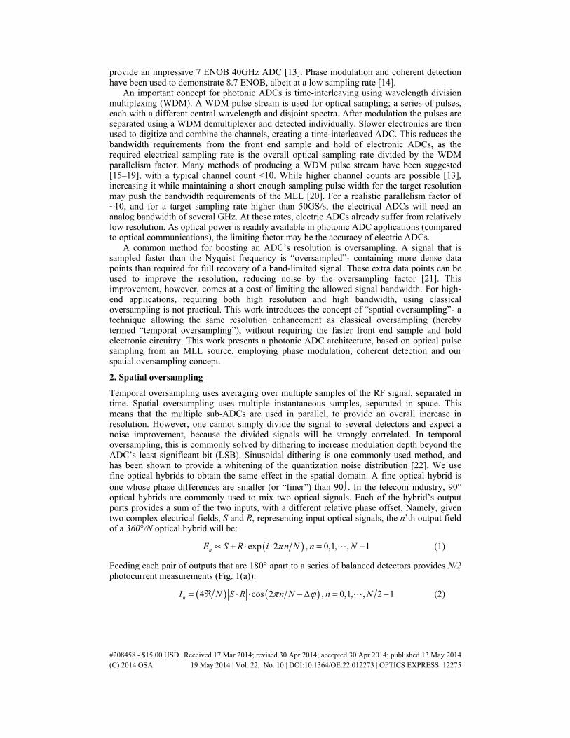
Fig. 1. (a) layout of a photonic ADC with information encoded on the optical phase, self-coherent detection with an optical hybrid supporting spatial oversampling. (b) Discernible phase states in the I/Q plane using 3 bit ideal quantizers and for N = 4 (i), 8 (ii), 16 (iii).
Denoting the I/Q noise terms i and q respectively, and using the fact that εn are independent, the I/Q noise variances become:
( )( )
2/2 12 2
20
var( ) cos 22 4var
var( ) sin 2
N
n
i n Nq n NN N
πσ σ
π
−
=
= ⋅ = (10)
As i and q have equal variances, the phase SNR can be easily obtained:
#208458 - $15.00 USD Received 17 Mar 2014; revised 30 Apr 2014; accepted 30 Apr 2014; published 13 May 2014(C) 2014 OSA 19 May 2014 | Vol. 22, No. 10 | DOI:10.1364/OE.22.012273 | OPTICS EXPRESS 12277

224
NSNRϕ πσ
= ⋅ (11)
The π2 factor in Eq. (11) comes from assuming the input phase is distributed equally across the [-π, π] range. We learn from Eq. (11) that the SNR improves by 3dB for every doubling of N, corresponding to half an ENOB improvement. In terms of overall ENOB performance of the photonic ADC with spatial oversampling, Eq. (11) leads to:
( )12 22log log 4ENOB B Nπ= + + (12)
The second term in Eq. (12) shows the resolution improvement of using phase modulation (compared to amplitude modulation), and the third term is attributed to spatial oversampling. As the minimal required ports is N = 4 (90° hybrid), N/4 (with N≥4) becomes the oversampling factor. This result is identical to temporal oversampling, where doubling the oversampling factor adds half an ENOB of resolution [16].
It is worthy to contemplate a simpler alternative method to achieve spatial oversampling- Using a single standard 90° optical hybrid and a series of power splitters at its outputs, splitting the signal to N output points, can achieve similar results. In the detection noise limited case, the noise at each detection point can be considered as independent even if the noiseless quantities are identical, hence averaging over these measurements will provide the same noise reduction as provided by a fine optical hybrid. However, this approach does not contribute in the quantization noise limited case, providing no improvement at all. For intermediate cases, where the ENOB is only slightly lower than the number of bits, using a single 90° hybrid and power splitters will provide some improvement, but considerably less than our fine optical hybrids.
3. Interferometric oversampling system design
Many ways exist to implement a fine optical hybrid [26–28]. Our optical hybrids are based on the star-coupler design [29], as it is highly suitable for large port counts and, respectively, a high oversampling factor (Fig. 2(a)). The two inputs are placed symmetrically about the optical axis of a confocal slab lens, separated by distance d. The field at the input plane may be expressed as the two input signals’ amplitude and position convolved with the waveguides' mode, which is assumed to be Gaussian.
( ) ( ) ( )2 2( ) exp 2 2E S d R dξ ξ δ ξ δ ξ= − Δ ⊗ ⋅ + + ⋅ − (13)
where ξ denotes the spatial coordinate of the curved input plane, Δ the waveguide mode width, and δ is the Dirac delta function. At the curved output plane of the slab lens the Fourier transforms of the input signals are interfered. The power at the curved output plane is:
( ) ( )( )2
2 2
22 cos 2 expx
xP x R S S R f xW
π ϕ ∝ + + ⋅ + Δ ⋅ −
(14)
where x is the spatial coordinate of the curved output plane, ( )0 02xf n d Lλ= ,
( )0 04W L nπ λ= Δ , L is the slab lens radius, and n0 the refractive index. Placing the output
waveguides within the [-1/(2fx), 1/(2fx)] range determines the output interference relations. For the case of a 360°/N optical hybrid, the N output waveguides will be placed at:
( ) ( )2 1 2 1, ,n xx n N N f n N= − − ⋅ = (15)
To accommodate higher output port counts, we can increase the slab lens size L. As we use short optical pulses, the path lengths of the two interfering arms must be
matched and phase-stabilized. Otherwise, the signal and reference pulses might have poor temporal overlap, and no phase information will be detected. This bars the use of off-the-shelf
#208458 - $15.00 USD Received 17 Mar 2014; revised 30 Apr 2014; accepted 30 Apr 2014; published 13 May 2014(C) 2014 OSA 19 May 2014 | Vol. 22, No. 10 | DOI:10.1364/OE.22.012273 | OPTICS EXPRESS 12278
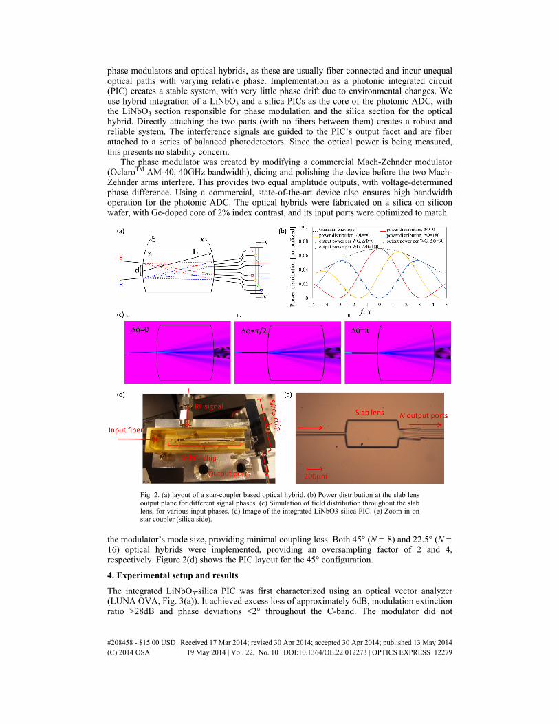
phase modulators and optical hybrids, as these are usually fiber connected and incur unequal optical paths with varying relative phase. Implementation as a photonic integrated circuit (PIC) creates a stable system, with very little phase drift due to environmental changes. We use hybrid integration of a LiNbO3 and a silica PICs as the core of the photonic ADC, with the LiNbO3 section responsible for phase modulation and the silica section for the optical hybrid. Directly attaching the two parts (with no fibers between them) creates a robust and reliable system. The interference signals are guided to the PIC’s output facet and are fiber attached to a series of balanced photodetectors. Since the optical power is being measured, this presents no stability concern.
The phase modulator was created by modifying a commercial Mach-Zehnder modulator (OclaroTM AM-40, 40GHz bandwidth), dicing and polishing the device before the two Mach-Zehnder arms interfere. This provides two equal amplitude outputs, with voltage-determined phase difference. Using a commercial, state-of-the-art device also ensures high bandwidth operation for the photonic ADC. The optical hybrids were fabricated on a silica on silicon wafer, with Ge-doped core of 2% index contrast, and its input ports were optimized to match
Fig. 2. (a) layout of a star-coupler based optical hybrid. (b) Power distribution at the slab lens output plane for different signal phases. (c) Simulation of field distribution throughout the slab lens, for various input phases. (d) Image of the integrated LiNbO3-silica PIC. (e) Zoom in on star coupler (silica side).
the modulator’s mode size, providing minimal coupling loss. Both 45° (N = 8) and 22.5° (N = 16) optical hybrids were implemented, providing an oversampling factor of 2 and 4, respectively. Figure 2(d) shows the PIC layout for the 45° configuration.
4. Experimental setup and results
The integrated LiNbO3-silica PIC was first characterized using an optical vector analyzer (LUNA OVA, Fig. 3(a)). It achieved excess loss of approximately 6dB, modulation extinction ratio >28dB and phase deviations <2° throughout the C-band. The modulator did not
#208458 - $15.00 USD Received 17 Mar 2014; revised 30 Apr 2014; accepted 30 Apr 2014; published 13 May 2014(C) 2014 OSA 19 May 2014 | Vol. 22, No. 10 | DOI:10.1364/OE.22.012273 | OPTICS EXPRESS 12279
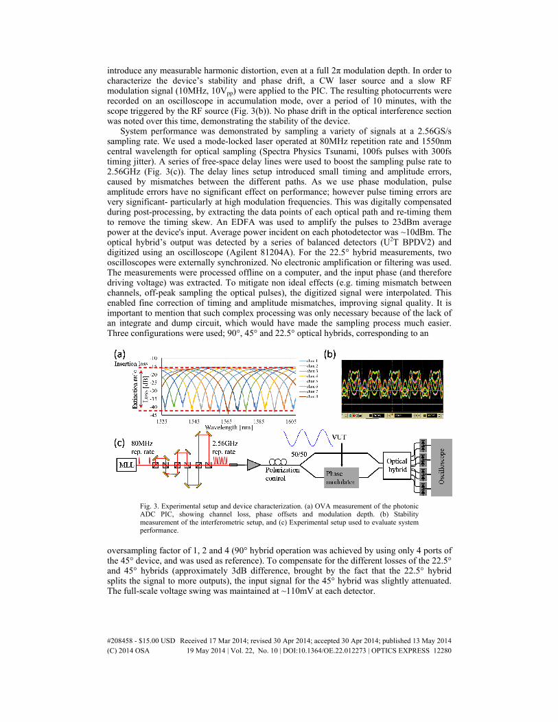
introduce any measurable harmonic distortion, even at a full 2π modulation depth. In order to characterize the device’s stability and phase drift, a CW laser source and a slow RF modulation signal (10MHz, 10Vpp) were applied to the PIC. The resulting photocurrents were recorded on an oscilloscope in accumulation mode, over a period of 10 minutes, with the scope triggered by the RF source (Fig. 3(b)). No phase drift in the optical interference section was noted over this time, demonstrating the stability of the device.
System performance was demonstrated by sampling a variety of signals at a 2.56GS/s sampling rate. We used a mode-locked laser operated at 80MHz repetition rate and 1550nm central wavelength for optical sampling (Spectra Physics Tsunami, 100fs pulses with 300fs timing jitter). A series of free-space delay lines were used to boost the sampling pulse rate to 2.56GHz (Fig. 3(c)). The delay lines setup introduced small timing and amplitude errors, caused by mismatches between the different paths. As we use phase modulation, pulse amplitude errors have no significant effect on performance; however pulse timing errors are very significant- particularly at high modulation frequencies. This was digitally compensated during post-processing, by extracting the data points of each optical path and re-timing them to remove the timing skew. An EDFA was used to amplify the pulses to 23dBm average power at the device's input. Average power incident on each photodetector was ~10dBm. The optical hybrid’s output was detected by a series of balanced detectors (U2T BPDV2) and digitized using an oscilloscope (Agilent 81204A). For the 22.5° hybrid measurements, two oscilloscopes were externally synchronized. No electronic amplification or filtering was used. The measurements were processed offline on a computer, and the input phase (and therefore driving voltage) was extracted. To mitigate non ideal effects (e.g. timing mismatch between channels, off-peak sampling the optical pulses), the digitized signal were interpolated. This enabled fine correction of timing and amplitude mismatches, improving signal quality. It is important to mention that such complex processing was only necessary because of the lack of an integrate and dump circuit, which would have made the sampling process much easier. Three configurations were used; 90°, 45° and 22.5° optical hybrids, corresponding to an
Fig. 3. Experimental setup and device characterization. (a) OVA measurement of the photonic ADC PIC, showing channel loss, phase offsets and modulation depth. (b) Stability measurement of the interferometric setup, and (c) Experimental setup used to evaluate system performance.
oversampling factor of 1, 2 and 4 (90° hybrid operation was achieved by using only 4 ports of the 45° device, and was used as reference). To compensate for the different losses of the 22.5° and 45° hybrids (approximately 3dB difference, brought by the fact that the 22.5° hybrid splits the signal to more outputs), the input signal for the 45° hybrid was slightly attenuated. The full-scale voltage swing was maintained at ~110mV at each detector.
#208458 - $15.00 USD Received 17 Mar 2014; revised 30 Apr 2014; accepted 30 Apr 2014; published 13 May 2014(C) 2014 OSA 19 May 2014 | Vol. 22, No. 10 | DOI:10.1364/OE.22.012273 | OPTICS EXPRESS 12280
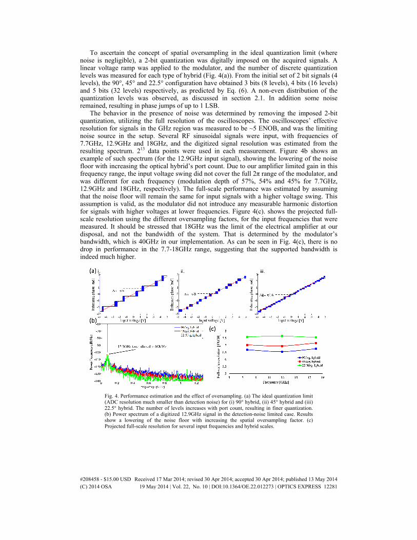
To ascertain the concept of spatial oversampling in the ideal quantization limit (where noise is negligible), a 2-bit quantization was digitally imposed on the acquired signals. A linear voltage ramp was applied to the modulator, and the number of discrete quantization levels was measured for each type of hybrid (Fig. 4(a)). From the initial set of 2 bit signals (4 levels), the 90°, 45° and 22.5° configuration have obtained 3 bits (8 levels), 4 bits (16 levels) and 5 bits (32 levels) respectively, as predicted by Eq. (6). A non-even distribution of the quantization levels was observed, as discussed in section 2.1. In addition some noise remained, resulting in phase jumps of up to 1 LSB.
The behavior in the presence of noise was determined by removing the imposed 2-bit quantization, utilizing the full resolution of the oscilloscopes. The oscilloscopes’ effective resolution for signals in the GHz region was measured to be ~5 ENOB, and was the limiting noise source in the setup. Several RF sinusoidal signals were input, with frequencies of 7.7GHz, 12.9GHz and 18GHz, and the digitized signal resolution was estimated from the resulting spectrum. 213 data points were used in each measurement. Figure 4b shows an example of such spectrum (for the 12.9GHz input signal), showing the lowering of the noise floor with increasing the optical hybrid’s port count. Due to our amplifier limited gain in this frequency range, the input voltage swing did not cover the full 2π range of the modulator, and was different for each frequency (modulation depth of 57%, 54% and 45% for 7.7GHz, 12.9GHz and 18GHz, respectively). The full-scale performance was estimated by assuming that the noise floor will remain the same for input signals with a higher voltage swing. This assumption is valid, as the modulator did not introduce any measurable harmonic distortion for signals with higher voltages at lower frequencies. Figure 4(c). shows the projected full-scale resolution using the different oversampling factors, for the input frequencies that were measured. It should be stressed that 18GHz was the limit of the electrical amplifier at our disposal, and not the bandwidth of the system. That is determined by the modulator’s bandwidth, which is 40GHz in our implementation. As can be seen in Fig. 4(c), there is no drop in performance in the 7.7-18GHz range, suggesting that the supported bandwidth is indeed much higher.
Fig. 4. Performance estimation and the effect of oversampling. (a) The ideal quantization limit (ADC resolution much smaller than detection noise) for (i) 90° hybrid, (ii) 45° hybrid and (iii) 22.5° hybrid. The number of levels increases with port count, resulting in finer quantization. (b) Power spectrum of a digitized 12.9GHz signal in the detection-noise limited case. Results show a lowering of the noise floor with increasing the spatial oversampling factor. (c) Projected full-scale resolution for several input frequencies and hybrid scales.
#208458 - $15.00 USD Received 17 Mar 2014; revised 30 Apr 2014; accepted 30 Apr 2014; published 13 May 2014(C) 2014 OSA 19 May 2014 | Vol. 22, No. 10 | DOI:10.1364/OE.22.012273 | OPTICS EXPRESS 12281
5. Conclusion and discussion
We proposed and demonstrated the concept of spatial oversampling, a mathematical equivalent to classic temporal oversampling. The concept trades the excess bandwidth of temporal oversampling for increased parallelism, allowing resolution improvement without bandwidth loss. Spatial oversampling has been shown to both increase the number of quantization levels (dominant effect when using low resolution ADCs) and lower the noise floor (dominant effect when using high resolution ADCs). Oversampling factors of 2 and 4 were demonstrated with 45° and 22.5° optical hybrids, corresponding to a resolution increase of 0.5 and 1 ENOB, compared to a standard 90° optical hybrid. Based on this concept, we demonstrated quantization of RF signals, with frequencies up to 18GHz. A maximal full-scale resolution of 7.6 ENOB was achieved.
This performance improvement does come at a cost of increasing system complexity and the amount required hardware. While high oversampling factors using discrete components are not practical, combining this technology with integrated electronic circuitry (e.g. on a silicon photonics platform) can make it feasible for commercial systems.
It should be noted that the results presented here are by no means the limit of this technique. Modulation frequencies were limited by the electrical amplifier we used, and overall resolution was limited by the relatively low ENOB of the oscilloscopes at our disposal. Using designated integrate and dump circuits will also greatly improve fidelity. The spatial oversampling technique continues to be an effective method for increasing the conversion fidelity when higher performing (lower ENOB) electrical ADC are employed.
#208458 - $15.00 USD Received 17 Mar 2014; revised 30 Apr 2014; accepted 30 Apr 2014; published 13 May 2014(C) 2014 OSA 19 May 2014 | Vol. 22, No. 10 | DOI:10.1364/OE.22.012273 | OPTICS EXPRESS 12282