Embed Size (px)
Citation preview

1 Copyright © 20xx by ASME
Proceedings of IMECE2007 2007 ASME International Mechanical Engineering Congress and Exposition
November 11-15, 2007, Seattle, Washington, USA
IMECE2007-42752
A ONE-DIMENSIONAL MODEL CAPTURING SELECTIVE ION TRANSPORT EFFECTS IN NANOFLUIDIC DEVICES
Brice T. Hughes Mechanical Engineering Dept. &
Nano Tech Center Texas Tech University
Lubbock, TX 79409 [email protected]
Jordan M. Berg Mechanical Engineering Dept. &
Nano Tech Center Texas Tech University
Lubbock, TX 79409 [email protected]
Darryl L. James Mechanical Engineering Dept. &
Nano Tech Center Texas Tech University
Lubbock, TX 79409 [email protected]
Akif Ibraguimov
Dept. of Mathematics & Statistics
Texas Tech University Lubbock, TX 79409
Shaorong Liu Dept. of Chemistry &
Biochemistry Texas Tech University
Lubbock, TX 79409
Henryk Temkin Electrical Engineering Dept. &
Nano Tech Center Texas Tech University
Lubbock, TX 79409
ABSTRACT This paper presents a numerical model of one-dimensional,
steady-state, multi-species, ion transport along a channel of variable width and depth. It is intended for computationally efficient simulation of devices with large variations in characteristic length scale—for example those incorporating both micro- and nanochannels. The model represents both volume charge in the fluid and surface charge on the channel walls as equivalent linear charge densities. The relative importance of the surface terms is captured by a so-called “overlap parameter” that accounts for electric double-layer effects, such as selective ion transport. Scale transitions are implemented using position-dependent area and perimeter functions. The model is validated against experimental results previously reported in the literature. In particular, model predictions are compared to measurements of fluorescent tracer species in nanochannels, of nanochannel conductivity, and of the relative enhancement and depletion of negatively and positively charged tracer species in a device combining micro- and nanochannels. Surface charge density is a critical model parameter, but in practice it is often poorly known. Therefore it is also shown how the model may be used to estimate surface charge density based on measurements. In two of the three experiments studied the externally applied voltage is low, and excellent results are achieved with electroosmotic terms neglected. In the remaining case a large external potential (~ 1 kV) is applied, necessitating an additional adjustable parameter to capture convective transport. With this addition, model performance is excellent.
INTRODUCTION As fluidic devices shrink into the nanometer regime, the
ratio of channel surface area to volume increases and surface forces that are typically negligible at the millimeter or micrometer scale can become dominant. These effects may be exploited to create entirely new functionalities. A wide variety of devices and applications are reported in the literature, as surveyed for example in [1,2]. Specific applications include DNA analysis [3,4], analyte separation [5–8], power generation [9–14], and flow control [15]. Fabrication of nanofluidic devices is still a delicate art, and experiments are complicated by both small detection volumes, and by practical issues such as fouling [1]. Thus reliable and efficient numerical models to reduce reliance on trial-and-error could significantly facilitate device development.
Efficient numerical simulation of nanofluidic devices is made challenging by the large range of scales encountered. It is not unusual, for example, that a nanochannel have a depth of tens of nanometers, a width of tens or hundreds of micrometers, and a length of several millimeters, or even centimeters. Standard finite-element or finite-volume approaches lead to large meshes, long solution times, and high demands on computational resources. Devices with multiple feature scales, such as those combining micro- and nanochannels, compound this difficulty. Thus most numerical models consider only one or two dimensions. Many such studies reported in the literature focus on simulation of properties in the smallest dimension—typically the channel depth [16–18]. However in many devices performance is determined by transport along the channel

2 Copyright © 20xx by ASME
length—typically the largest dimension. Accordingly, the goal of this paper is to develop and validate a one-dimensional model of species transport only along the channel length, but that nonetheless incorporates important physics due to the nanoscale dimension. Furthermore, to reflect the practical requirements of making external connections to nanochannels, as well as of storing, mixing, and collecting fluid, it is desired that the one-dimensional model handle transitions between channels of greatly different cross-sections.
Daiguji, Karnik, and coworkers have previously reported a two-dimensional simulation of through-channel properties, to examine effects of surface charge density variations, and predict the power generation and current rectification of a nanofluidic device [19–22]. However this model does not allow large area changes at micro- to nanochannel interfaces. Pennathur and Santiago present numerical and analytical models for analyte separation [5], however, these models also do not take into account micro- to nanoscale interfaces.
The one-dimensional, steady-state model developed below captures selective ion transport effects due to the electric double layer (EDL). It accomplishes this by representing both volume charge in the fluid and surface charge on the channel walls as equivalent linear charge densities. The relative importance of the surface terms is captured by a so-called “overlap parameter.” When the overlap parameter is large, the EDL thickness is large compared to a characteristic cross-channel dimension. When the overlap parameter is small, the EDL thickness is negligible compared to the channel depth.
Scale transitions are accommodated using position-dependent area and perimeter functions. The use of a one-dimensional model eliminates the problem of a high aspect ratio two-dimensional mesh, but rapid variations in area and/or perimeter require that the one-dimensional mesh be dense in those regions. To obtain convergence in such cases it was necessary to use continuation methods, that is, to gradually build the solution up from a less drastic starting geometry.
The one-dimensional model is validated against experimental results previously reported in the literature. In particular, the model predictions are compared to measurements of fluorescent tracer species in nanochannels, of nanochannel conductivity, and of the relative enhancement and depletion of negatively and positively charged tracer species in a device combining micro- and nanochannels [10,23].
Surface charge density is a critical parameter in this model, but in practice it is often poorly known. Therefore the paper also shows how the one-dimensional model may be used to estimate surface charge density based on measurements. In two of the three experimental studies considered the externally applied voltage is low, and excellent results are achieved without including electroosmotic terms. In the remaining case a large external potential (~ 1 kV) is applied, necessitating an additional adjustable parameter to capture convective transport. With this addition, model performance is excellent.
MODEL EQUATIONS The one-dimensional model is developed from the partial
differential equations of electrokinetic flow. Poisson’s equation is used to model the electrostatic potential and is coupled to the Nernst-Planck equation, which is used to model ionic concentrations for n species in solution. Throughout this section superscript * denotes a dimensional quantity and ~ denotes a dimensional operator.
The dimensional Poisson’s equation is
!
" ˜ # 2$* =
F
%s&
0
zini
i
' (1)
where φ* is the electric potential in volts, F is Faraday’s constant in C/mol, zi is the valence of ionic species i, ni is the concentration of species i, in mol/m3, κs is the dielectric constant of the solvent, and e0 is the permittivity of free space in C2/J-m. Equation (2) is the Nernst-Planck equation for species i.
**~~
* unnzRT
DFnDj iiiiii
+!"!"= # , (2)
where, *ij is the flux of species i in mol/m2-s, Di is the diffusion coefficient for species i in m2/s, R is the universal gas constant in kJ/mol-K, T is the absolute temperature in K, and u* is the mass average velocity of the bulk.
In a model of dimension two or higher, the surface charge density of the channel walls would appear as a boundary condition; however in the one-dimensional case the only boundaries are the channel entrance and exit. If the surface charge is to be considered it must be transferred into the domain and explicitly included in Poisson’s equation (1). This is accomplished by representing the surface charge density as an equivalent volume charge density term, ρv*, which is then included as a source term in the one-dimensional Poisson’s equation:
!
"d2#*
dx*2
=1
$s%0
{F zini
i
& + 'v*} . (3)
The added charge density term ρv* is found by equating the total charge in a fluid control volume with a specified specified surface charge density and no volume charges to one with only a volume charge density and no charged surfaces. Denoting the surface charge density by ρa*, the channel perimeter by P, and the channel cross-sectional area by A we obtain
!
"v* # "
a* P A( ) .
The one-dimensional Nernst-Planck equation is
!
j i*
= "Di
dni
dx*"DF
RTzini
d#*
dx*
+ niu* . (4)
Equations (3) and (4) are normalized with the following parameters:
!
" #" * "0
,
!
"i# z
iniI ,
!
u " u * uHS
,
!
x " x * L
!
,
!
" # RT F $0
,
!
" # $s%0RT F I , and
3 Copyright © 20xx by ASME
!
"i# u
HSL D
i, where the ionic strength, I is defined as
!i
iinz2
2
1 , the Helmholtz-Smoluchowski velocity, uHS, is
defined as sxs
E !"#$0
% , L is the nanochannel length, λ is the Debye length, Ex is the externally applied field, ηs is the solvent viscosity and ζ is the zeta potential. Note here that the normalized concentrations χi contain the valence zi, and so are signed, i.e., positive for cations and negative for anions.
The entire normalized system, including the normalized forms of the one-dimensional Poisson’s equation, Nernst-Planck equation, and conservation of mass, is as follows:
!"#
$%&
+=' (i
iya
xdx
d)µ*
µ
+,22
2
(5)
!
ji "L
DiIji* = #
1
zi
d$ i
dx#1
%$ i
d&
dx+' i
zi$ iu
(
) *
+
, - (6)
!
d
dx(Aji ) = 0 (7)
where
( )
RTI
PAl
l
baa
yy
x
0* !"##
$$µ
$µ
%
%%
%
The parameter µy is deserving of special comment. A/P is Dh/4, where Dh is the hydraulic diameter. This is a convenient geometry-independent measure of channel depth, equal to the diameter for a circular channel, or twice the depth for a shallow rectangular channel. Thus µy is 4λ/Dh. A large value indicates significant overlap between the channel double layers. A small value indicates negligible interaction between double layers. Hence we refer to µy as the overlap parameter.
Also of note is the average bulk velocity u appearing in (6). To the best of our knowledge, accurate numerical prediction of this term requires computing cross-channel ion profiles. However our goal is to avoid a two-dimensional analysis. Equating the average electrostatic and viscous body forces results in the Helmholtz-Smoluchowski velocity, uHS, given above. This is suitable in principle for a one-dimensional approach, but our experience suggests that it is not a good approximation to the bulk velocity when the channel varies in geometry. Therefore we take the following approach to handling the bulk velocity. We begin by assuming that it is negligible. This is reasonable when the externally-applied potential is small, and is in agreement with observations by Li [24] and Daiguji et al. [19]. When the applied external potential is large, we include the mass averaged bulk velocity as an adjustable parameter. As will be seen, it may be necessary to also treat the surface charge density as an adjustable parameter. In this case, rather than simultaneously choose values for both parameters we first pick the surface charge density based on measurements in the absence of an applied external field. Then we use that surface charge density value to subsequently
estimate u. The Helmholtz- Smoluchowski velocity provides a useful check on the plausibility of the result; u should not exceed uHS [5,25]. In the validation cases considered below, very good agreement was found between simulation and experiment without considering the bulk velocity, except when the external applied voltage was very high.
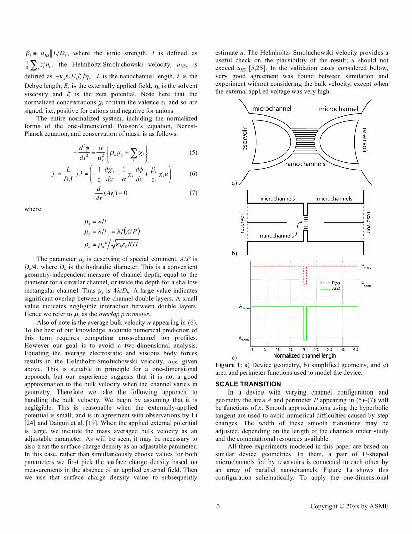
a)
b)
c) Figure 1: a) Device geometry, b) simplified geometry, and c) area and perimeter functions used to model the device.
SCALE TRANSITION In a device with varying channel configuration and
geometry the area A and perimeter P appearing in (5)–(7) will be functions of x. Smooth approximations using the hyperbolic tangent are used to avoid numerical difficulties caused by step changes. The width of these smooth transitions may be adjusted, depending on the length of the channels under study and the computational resources available.
All three experiments modeled in this paper are based on similar device geometries. In them, a pair of U-shaped microchannels fed by reservoirs is connected to each other by an array of parallel nanochannels. Figure 1a shows this configuration schematically. To apply the one-dimensional

4 Copyright © 20xx by ASME
model (5)–(7), the geometry is first simplified as shown in Fig. 1b. Finally, the simplified geometry is summarized by functions A(x) and P(x), as shown in Fig. 1c. Multiple parallel channels are handled by summing the individual areas and perimeters.
In particular, we model the three regions of the simulated device using the following transition functions:
!!"
#$$%
& ''=
(entryxx
xD tanh2
1
2
1)(1 (8)
!!"
#$$%
& ''!"
#$%
& '=
((
xxxxxD
entryexit tanh2
1tanh2
1)(2 (9)
!"
#$%
& ''=
(
xxxD
exittanh2
1
2
1)(3 (10)
Parameter δ is the transition width. Equations (8), (9), and (10) represent the left microchannels, the nanochannels, and the right microchannels, respectively. The area function is then constructed as follows:
!
A(x) = Amicro
D1 (x) +D3 (x){ } + Anano
D2 (x) (11)
where, Amicro and Anano are the total areas of the microchannel and nanochannel regions, respectively. The perimeter function is created in the same manner.
As described above, the bulk velocity u appearing in (6) is treated as an adjustable parameter in cases where a large external field is applied. When the area varies the bulk velocity will not be constant, so this term is modified by the area function by applying continuity for an incompressible flow:
!
u(x) " u*(x) u
HS
= u Anano
uHS
A(x) (12)
where
!
u is the adjustable parameter. Substituting (11) and (12) into (5)–(7) and defining µy = λP(x)/A(x) yields the final model equations,
!"#
$%&
+=' (i
iya
x
xdx
d)µ*
µ
+,)(
22
2
(13)
!
ji (x) = "1
zi
d# i
dx"1
$# i
d%
dx+&
zi
# i
u Anano
uHS A(x)
'
( ) )
*
+ , , (14)
( ) 0)()( =xAxjdx
di . (15)
SIMULATION RESULTS & MODEL VALIDATION We compare the results obtained through numerical
solution of (13)–(15) against three experimental results reported in the literature. In [23] Pu et al. suggest that EDL effects in nanochannel flows may be used to provide preferential ion transport. We model their device and compare our simulation results to two sets of measurements reported in [23]. The first is a fluorescence-based measurement of the concentration of a tracer species (fluorescein) in the nanochannel. The second is a
measurement of the relative enhancement and depletion of tracer species at the two ends of the nanochannel. Liu et al. use a similar device in [10] to determine the effect of channel geometry and bulk ionic concentrations on nanochannel conductivity. The third experimental validation of our model is a comparison of numerically predicted conductivities to the experimental results reported in [10].
These experiments are considered in individual detail below. Here we discuss elements common to all three. In each case (13)–(15) are solved numerically using the non-linear solver included in the commercial software package COMSOL Multiphysics [34]. Table 1 lists simulation parameters common to all of the cases.
Table 1: Common simulation parameters [26] Parameter Value Parameter Value
T 300 K ks 78.54 zNa 1 DNa 1.3×10⁻⁹ m2/s zBO4 –2 DBO4 1.0×10⁻⁹ m2/s zfluor –1 Dfluor 5.4×10⁻¹⁰ m2/s zH 1 DH 9.3×10⁻⁹ m2/s
zClO4 –1 DClO4 1.8×10⁻⁹ m2/s χi(0) χi,bulk χi(xmax) χi,bulk
Subscripts: Na, sodium; BO4, borate; fluor, fluorescein; H, hydrogen; ClO4, perchlorate.
Also common to the three cases is the need to apply continuation to obtain convergence. In all cases the Debye length λ is much smaller than the channel length, l. Thus the term µx = λ/l appearing in (13) is very small, and so (13) is singularly perturbed. Singularly perturbed problems are characterized by dynamics on multiple length scales [27,28]. These problems often present numerical difficulties, which may be resolved by first solving the equations at a more tractable parameter value, i.e., µx ≈ 1. A series of simulations is carried out, with the parameter value changed a small amount each time, and the solution from one step used as the initial guess for the next, until a solution for the desired parameter value is achieved. Typically 500 simulation steps were required for convergence, a process that took up to 4 hours on a AMD Athlon MP 2400+ with 3.0 GB of RAM.
Table 2: Boundary conditions for nanochannel concentration experiments from [23]
Parameter Symbol Value Device length L0 41 mm
Nanochannel length L 1 mm Applied external potential (dim) φ0* 0 V
Potential at x = 0 (non-dim) φ(0) 0 Potential at x = xmax (non-dim) φ(xmax) 0
Nanochannel Concentration Experiments: The devices used in [23] by Pu et al. consist of two reservoirs connected by a series of micro- and nanochannels. A U-shaped microchannel is connected to each reservoir, and parallel nanochannels

5 Copyright © 20xx by ASME
connect the two microchannels, as in the schematic of Fig. 1a. Each microchannel is 100 µm deep by 750 µm wide by 20 mm long. The U-channels are connected to each other by eight parallel nanochannels 60 nm deep by 100 µm wide by 1 mm long. The reservoirs are filled with identical buffer solutions containing fluorescein as a tracer species.
Figure 2: Effect of buffer concentration on tracer concentration for a range of surface charge densities. By using a range of surface charge densities, the experimental data was bracketed and interpolated between to obtain an estimated surface charge density. Triangles denote the average fluorescein concentration recorded by Pu et al. Tables 1 and 2 give simulation parameters and boundary conditions.
While the main goal of [23] is to examine the ion enhancement/depletion phenomenon under a strong externally-applied potential, fluorescence-based measurements to examine the effect of the sodium tetraborate buffer solution concentration on the fluorescein concentration inside the nanochannels are also reported. These experiments used no applied potential. The device itself was modeled as in Fig. 1. The boundary conditions at the reservoirs were buffer solution of sodium tetraborate with concentrations varying from 30 µM to 30 mM and fluorescein tracer with a fixed concentration of 30 µM. Simulation parameters and boundary conditions are listed in Tables 1 and 2. The simulation requires as a parameter the surface charge density ρa*. However this value is not well known. Therefore runs were made at each buffer concentration for surface charge densities of –2, –20 and –200 mC/m2. An interpolated value of –10.2 mC/m2 was then picked based on the best fit to the data. This is comparable to previously reported values [31,32]. Figure 2 shows the results.
The hypothesis presented in [23] is that the negatively charged fluorescein ions are excluded from the nanochannel (along with the negatively charged buffer ions) by the zone of negative potential associated with the EDL. As the buffer concentration decreases the EDL thickness increases, and the exclusion effect also increases. From Fig. 2 it is evident that the model accurately captures this behavior without the need to
explicitly model the EDL. In the absence of an external field there is no bulk velocity, so no error is introduced by omitting
!
u . If an accurate value for surface charge density is available a priori then no parameter fitting is required. However since the surface charge density is difficult to measure directly, this application of the one-dimensional model is potentially useful as a method for obtaining this important quantity.
Enhancement/Depletion Experiments: In [23] Pu et al. also examine the ion enhancement-depletion effect arising from Donnan exclusion [1,29]. The same device is used as for the nanochannel tracer ion concentration measurements, but a potential of up to 1 kV is applied across the reservoirs to induce flow of the ion species and bulk solution. Under the externally applied field, both negatively and positively charged ions deplete in the microchannel near the anode, and both negatively and positively charged ions accumulate in the microchannel near the cathode. This is explained by the selective transport of counter-ions through the nanochannel while co-ions are screened out by the Donnan exclusion effect.
Table 3: Boundary conditions for enhancement/depletion experiments from [23]
Parameter Symbol Value Device length L0 41 mm
Nanochannel length L 1 mm Applied external potential (dim) φ0* 1 kV
Potential at x = 0 (non-dim) φ(0) 0 Potential at x = xmax (non-dim) φ(xmax) 1
The effect is quantified using fluorescence intensity measured in the microchannel immediately adjacent to the nanochannel on both ends. The results are compared to the fluorescence signature in the microchannels with no applied field, which should correspond to the bulk tracer species concentration (in contrast to the value in the nanochannel discussed in the previous section). This allows the concentration of the tracer species in the microchannel to be inferred. In [23] only the maximum enhancement/depletion, corresponding to an applied potential of 1 kV, is reported. Tables 1 and 3 give the model simulation parameters used.
The surface charge density is required in this simulation as well, but since it has been estimated in the previous section for the same experimental conditions, that value of –10.2 mC/m2 is used again here. Unlike the previous section, the bulk velocity cannot be assumed negligible. To bound this term and to normalize the velocity term in (14) we must compute the Helmholtz-Smoluchowski velocity. This in turn requires a value for the zeta-potential, ζ. Rather than treat ζ as a new parameter, we can estimate it based on the surface charge density for various buffer and tracer concentrations. by using the the Grahamme equation [33]:
2
1
,0
* 1exp2!"
!#$
!%
!&'
(()
*
++,
-.//0
1223
4.= 5 6
i B
i
iBsaTk
eznTk
789: (16)

6 Copyright © 20xx by ASME
For the buffer and tracer concentrations reported in [23], and the surface charge density value of –10.2 mC/m2 extracted from the experimental data, we solve (16) numerically using the MATLAB function fzero [35]. This gives a ζ of approximately –110 mV, corresponding to a Helmholtz-Smoluchowski velocity of ~ 2 mm/s.
Figure 3: Normalized potential, tracer concentration, and buffer concentration profiles for the nanofluidic device. Concentrations are signed —positive for cations, negative for anions. The shaded region represents the nanochannel region. Tables 1 and 3 give boundary conditions and simulation parameters.
Calculating ion enhancement and depletion following [23], we define as follows an enhancement factor, EF, for species at concentrations greater than their bulk value, and a depletion factor, DF, for species at a concentration below their bulk value:
!
EF =C final "Cbulk
Cbulk
(17)
final
finalbulk
C
CCDF
!= (18)
In [23] Pu et al. report an EF of approximately 100 and a DF of approximately 500. The simulation results are shown in Fig. 3, with the bulk velocity adjusted to best match the measured enhancement/ depletion result. The numerical results of Fig. 3 correspond to an EF of 126 and a DF of 500. The resulting value of bulk velocity is 17 µm/s.
The simulated enhancement/depletion values match the reported measured values well. However the estimated bulk velocity is so much smaller than the Helmholtz-Smoluchowski velocity that it raises the question of whether this parameter significantly affects the result. In fact, the concentration profiles are quite sensitive to the value of bulk velocity, as can be seen in Fig. 4, where concentration profiles are computed for bulk velocities of 0 µm/s, 17 µm/s, and 25 µm/s.
Figure 3 shows that at steady state the enhancement/ depletion effect is manifested throughout the entire length of the microchannels. The potential profile suggests that in the left microchannel, on the cathode side, the large build up of ions due to enhancement increases the microchannel conductance. Thus we see almost no potential rise on this side between the reservoir and the nanochannel. In the right hand microchannel, on the anode side, depletion makes the microchannel less conductive, hence the potential increases with a much steeper slope. This result suggests that accurate modeling of this effect at the device level should include not just the nanochannel, but the rest of the fluidic system as well.
Figure 4: Simulated signed concentration of the tracer species showing sensitivity to bulk velocity.
Figure 5: Normalized species flux throughout the device. The flux jumps at the nanochannel due to the area change between the micro- and nanochannels, but the mass flow rate of each species, A(x)ji(x), is constant.
The ultimate purpose of the model presented here is not to reproduce existing measurements, but to make predictions that

7 Copyright © 20xx by ASME
are useful for device design. As an example, a device such as was considered in this section might be used for selective ion transport. The results shown in Fig. 3 may now be used to predict the differential flux between species. Figure 5 shows a transport rate imbalance for this nanofluidic device, with cations experiencing preferential transport over anions. The predicted transport rate of cations is 26.9 fmol/s toward the cathode and that of anions is 7.32 fmol/s toward the anode. These values may be used to evaluate the suitability of a particular device for a potential application, or they may be used comparatively, for design optimization.
Nanochannel Conductivity Experiments: In [10] Liu et al. use devices similar those in the previous sections to demonstrate the increased proton conductivity of nanochannel structures. In this device, reservoirs terminate each end of the U-channel instead of both ends of a U-channel terminating into the same reservoir. Each U-shaped microchannel is 100 µm deep by 1 mm wide by 20 mm long. The pair of U-shaped microchannels is connected by an array of 55 parallel channels. In [10] these channel depths are varied from 50 nm to 250 µm to study the resulting effect on conductivity. We refer to these 55 parallel channels as the “nanochannel array” with the understanding that the deeper structures are not, strictly speaking, nanochannels.
Table 4: Boundary conditions for nanochannel conductance experiments from [10]
Parameter Symbol Value Nanochannel length L 1 mm
Applied external potential (dim) φ0* 1 V Potential at x = 0 (non-dim) φ(0) 0
Potential at x = xmax (non-dim) φ(xmax) 1
In [10] instantaneous conductance measurements were made for two different concentrations of a perchloric acid buffer solution across nanochannel arrays of various depths. The conductivity was calculated from the measured conductance using the known length and area of the nanochannel array. Because the measurements were made rapidly, and the system was not allowed to come to steady state, we consider the ion concentrations in the microchannels to be constant at the bulk reservoir concentration and model only the nanochannel region. The parameters and boundary conditions used in the simulation are given in Tables 1 and 4. It is stated that the surface has been treated to increase the charge density, but the value itself is unknown. Therefore we again use this parameter to fit the simulation results to the data. Current, i, can be calculated from the dimensional ionic flux by
!
i = zi ji * AFi" ; where, zi is the valence, ji* is the dimensional
flux, A is the area function and F is Faraday’s constant. The calculated ionic current and externally applied potential drop is used to find the conductance, K, and the conductivity by the equation
!
"H +
,app= KL A( ) 1 n
H +( ) , where, L is the nanochannel
length, A is the area function, and +Hn is the bulk proton
concentration. The result is referred to as the “apparent proton conductivity” but it includes contributions from all charged species. Figure 6 shows the simulation results at the optimal values of surface charge density, compared to the experimental data reported in [10].
Figure 6: Nanochannel proton apparent conductivity for a buffer of 10 µM and 1 mM HClO4. The triangles represent the average proton apparent conductivity recorded in [10] by Liu et al. for 10 µM HClO4 and the squares represent the average for 1 mM HClO4. Tables 1 and 4 give simulation parameters and boundary conditions.
The simulation gives good results, but to do so the two cases required substantially different estimates of surface charge density. These were –1 mC/m2 for the 10 µM HClO4 buffer and –40 mC/m2 for the 1 mM HClO4 buffer. Both of these are within the range reported in the literature [31,32]. The large difference between the cases is still a subject of interest, but we note that the observed trend, in which the effective surface charge density decreases with buffer concentration, is consistent with observations reported in the literature [32]. Because of the low external field applied, the bulk velocity has minimal effect on the results. CONCLUSIONS A one-dimensional, steady-state numerical model has been developed to predict multi-species ion transport in fluidic devices incorporating nanochannels. Application of the model to three experiments reported in the literature by Pu et al. [23] and Liu et al. [10] show that the model can capture effects attributable to the EDL without requiring simulation of cross-channel potentials or species profiles. If the surface charge density is not known a priori it must be fit to data. If the externally applied voltage is high enough, the bulk velocity must also be fit to data. This model directly predicts transport performance, and promises greater computational efficiency than two-dimensional simulations, especially across greatly varying length scales.

8 Copyright © 20xx by ASME
ACKNOWLEDGMENTS This work was partially supported by NSF grant CHE-
0514706 and the J. F. Maddox Foundation.
REFERENCES 1. Eijkel, Jan C.T.; van den Berg, A. Microfluidics and Nanofluidics 2005, Vol. 1, Iss.3, 249-267 2. Hu, G.; Li, D.; Chemical Engineering Science 2007, 62: 3443-3454 3. Guo, LJ; Cheng, X; Chou, C. Nano Letters 2004, 4, 1, 69-73 4. Tegenfeldt et al. Analytical and Bioanalytical Chemistry 2004, 378: 1678-1692 5. Pennathur, S., Santiago, J. G., Anal. Chem. 2005, 77: 6772–6781 6. Pennathur, S., Santiago, J. G., Anal. Chem. 2005, 77: 6782–6789 7. Yuan et al. Electrophoresis 2007, 28: 595-610 8. Garcia et al. Lab Chip 2005, 5: 1271-1276 9. Daiguji et al. Electrochemistry Communications. 2006, 8: 1796-1800 10. Liu et al. Nano Letters 2005, 5, 7, 1389-1393 11. van der Heyden et. al. Nano Letters 2007, 7, 4, 1022-1025 12. Yang et al. Journal of Micromechanics and Microengineering 2003, 13: 963-970 13. van der Heyden, FHJ; Stein, D; Dekker, C; Physical Review Letters 2005, 95: 1161104 14. van der Heyden et al. Nano Letters 2006, 6, 10, 2232-2237 15. Karlsson et al. Langmuir 2002, 18: 4186-4190 16. Conlisk et al. Anal. Chem. 2002, 74: 2139-2150 17. Zheng et al. Electrophoresis 2003, 24: 3006-3017 18. Conlisk, A. T. Electrophoresis 2005, 26: 1896-1912 19. Daiguji et al. Nano Letters 2004, 4, 1, 137-142 20. Karnik et al. Nano Letters 2005, 5, 5, 943-948 21. Daiguji et al. Nano Letters 2005, 5, 11, 2274-2280 22. Karnik et al. Nano Letters 2007, 7, 3, 547-551 23. Pu et al. Nano Letters 2004, 4, 6, 1099-1103 24. Li, Dongqing. Electrokinetics in Microfluidics, 1st ed., 2004, Elsevier Academic Press, London 25. Santiago, J.G. Anal. Chem. 2001, 73, 2353-2365 26. Dean, J.A. Lange’s Handbook of Chemistry, 12th ed., 1979, McGraw-Hill, Blacklick 27. Lin, C.C.; Segel, L.A. Mathematics Applied to Deterministic Problems in the Natural Sciences, 1988, SIAM, Philadelphia 28. Bender, C.M.; Orszag, S.A. Advanced Mathematical Methods for Scientists and Engineers: Asymptotic Methods and Perturbation Theory, 1999, Springer Science, New York 29. Hiemenz, P.C.; Rajagopalan, R. Principles of Colloid and Surface Chemistry, 3rd ed., 1997, Marcel Dekker, New York 30. Sjoback et. al. Spectrochimica Acta A, 1995, 51:L7-21 31. Sonnefeld, J. Journal of Colloid and Interface Science, 1996, 183: 597-599 32. Behrens, S.H.; Grier, D.G. Journal of Chemical Physics, 2001, 115, 14: 6716-6721 33. Berli, Claudio L.A.; Piaggio, Maria V.; Deiber, Julio A.; Electrophoresis 2003, Vol. 24, 1587-1595
34. COMSOL Multiphysics User’s Guide Version 3.2, COMSOL AB. 2005 35. MATLAB User’s Guide Version 7.1, The Mathworks Inc., Nattick, MA, 2005