Embed Size (px)
Citation preview
International Journal of Advanced Research in
Electrical and Electronics Engineering
Volume: 1 Issue: 1 08-Jun-2013,ISSN_NO: 2321-4775
1
A Novel Approach for Low-EMI and UPF Uninterruptible
Power Supply
R.Dhanasekaran and M.Murugan
Research Scholar Post Graduate Student
Department of Electrical and Electronics,
Government College of Technology, Anna University,
Coimbatore-641 013,Tamil Nadu, INDIA [email protected] and [email protected]
Abstract
A novel line interactive UPS
configuration is investigated that offers the
characteristics of an on-line or inverter
preferred UPS that features low-EMI and
draws Unity Power Factor (UPF) without the
addition of a pre-regulator at a reduced cost.
This new UPS is based on combination of two
full bridge VSI converters, one series with the
input, and other parallel to the load. The UPS
acts as a line conditional and output voltage
stabilizer. The series converter sees only a
small percentage of the input voltage.
Therefore small kVA rating, which results
reduced system cost compared conventional
on-line system cost compared conventional
on-line system and a new high frequency dc-
dc converter is proposed, which is based on a
half bridge series resonant converter. The
converter features Zero Voltage turn on,
snubbed turn off at reduced current for the
switching device and operating at switching
frequency higher than 20kHz. The efficiency
of the converter is very high under full load
and low load conditions, so total component
converter structure exhibits high efficiency.
Index Terms-- UPS, ZCS, ZVS, EMI .
I. INTRODUCTION
On-line UPS find wide applications
today, in critical loads like computer,
hospitals and airline reservation system need
Uninterruptible Power Supply. UPS provide
protection against power outage as well as
voltage regulation during power line over voltage
and under voltage condition. However it may
generate EMI and input power factor can be very
poor. EMI is the degradation in the performance of a device, or
equipment caused by an electromagnetic
disturbance. Power factor also has another serious
and undesirable effect on the power supply.
Therefore we have to reduce EMI and improve
the power factor is important. Traditionally quick
solutions to EMI and low power factor have been
brought about by introducing filters and pre-
regulator to existing equipment [1]. This had the
effect of increasing the cost of the system and
output link voltage making reduction of EMI
even more difficult. This thesis describes a UPS
topology specifically structured to have both
Unity Power Factor and Low- Electro Magnetic
Interference. The design is based on the principle
of Zero Current Switching (ZCS) and Zero
Voltage Switching (ZVS) as well as
incorporating internal waveform shaping
modules.
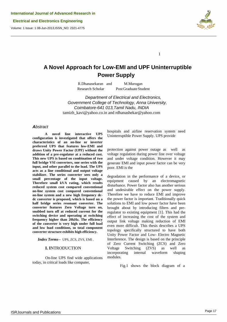
Fig.1 shows the block diagram of a
ISRJournals and Publications Page 17

International Journal of Advanced Research in
Electrical and Electronics Engineering
Volume: 1 Issue: 1 08-Jun-2013,ISSN_NO: 2321-4775
typical unity power factor On-line UPS with
galvanic isolation. The design includes a
pre-regulator on the input after the mains
rectifier, which shapes the current waveform
by high frequency modulation to obtain
Unity Power Factor. In the process, the
rectified input voltage is converted to a dc
voltage. This dc voltage is inverted to a high
frequency transformer, which also provides
galvanic isolation. The secondary voltage is
rectified to charge the battery and supply the
output dc link voltage. This voltage is
inverted by a pulse-width modulation
inverter to supply 230V at 50Hz, to the
load.
ISRJournals and Publications Page 18
International Journal of Advanced Research in
Electrical and Electronics Engineering
Volume: 1 Issue: 1 08-Jun-2013,ISSN_NO: 2321-4775
AC supply Load
Rectifier Pre-regulator H.F.Inv Rectifier PWM Inv
Fig.1.Block Diagram of Conventional UPS
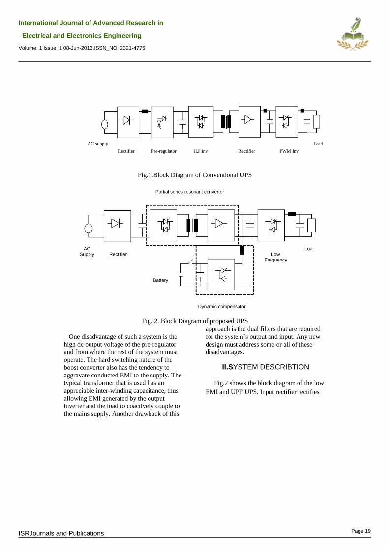
Partial series resonant converter
AC Loa Supply Rectifier Low
Frequency
Battery
Dynamic compensator
Fig. 2. Block Diagram of proposed UPS
approach is the dual filters that are required
One disadvantage of such a system is the
high dc output voltage of the pre-regulator
and from where the rest of the system must
operate. The hard switching nature of the
boost converter also has the tendency to
aggravate conducted EMI to the supply. The
typical transformer that is used has an
appreciable inter-winding capacitance, thus
allowing EMI generated by the output
inverter and the load to coactively couple to
the mains supply. Another drawback of this
for the system’s output and input. Any new
design must address some or all of these
disadvantages.
II. SYSTEM DESCRIBTION
Fig.2 shows the block diagram of the low
EMI and UPF UPS. Input rectifier rectifies
ISRJournals and Publications Page 19
International Journal of Advanced Research in
Electrical and Electronics Engineering
Volume: 1 Issue: 1 08-Jun-2013,ISSN_NO: 2321-4775
the main input voltage to dc voltage. Then
a dc-to- dc converter, the Partial Series Resonant Converter (PSRC) [2], to a high
frequency ac voltage, which passes through a transformer to provide galvanic isolation,
inverts the dc voltage. The pulsed dc voltage is inverted to 50Hz, 230V ac by a low
frequency inverter that supplies the load. Any reactive power from the load is
absorbed by a bi-directional dc-to-dc
converter connected in parallel to the
capacitor (C4), which acts as a compensator
and with typical voltage and current waveform. The second function of this bi- directional inverter is to charge the battery and, in the event of a mains failure, to provide power for the load. This converter will be referred to as “dynamic compensator”.
ISRJournals and Publications Page 20
International Journal of Advanced Research in
Electrical and Electronics Engineering
Volume: 1 Issue: 1 08-Jun-2013,ISSN_NO: 2321-4775
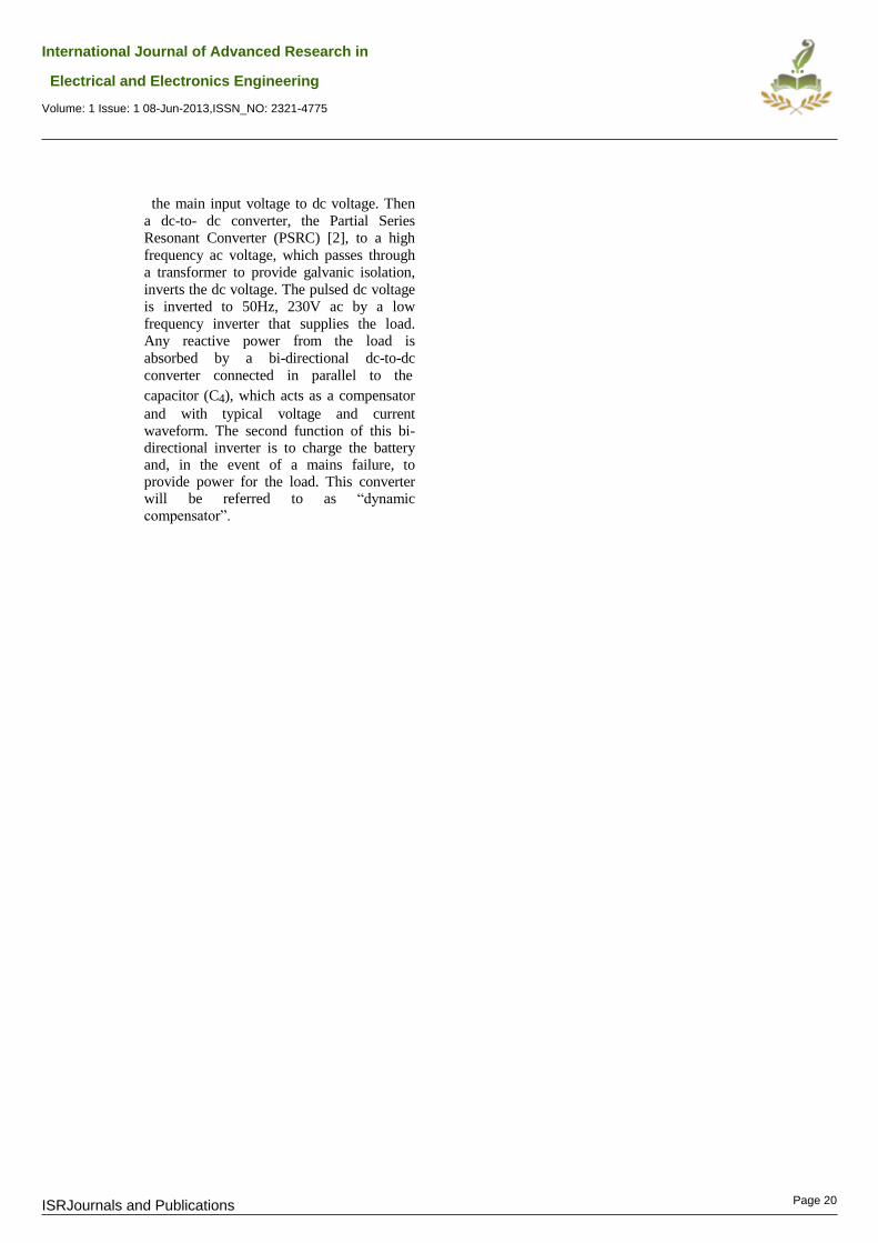
3
Fig.3 Power Circuit of Low EMI & UPF UPS voltage of 100Hz. This is achieved by small
capacitor (C1) after the diode bridge, which
is typically 1µF.
III. POWER CIRCUIT AND
OPERATION
The power circuit consists following four
main sections:
1. An input rectifier
2. A dc-to-dc ZCS-PSRC,
including the high frequency
rectifier
3. A dynamic compensator
4. An output rectifier
A. Input Rectifier
The input rectifier converts the
230V, 50 Hz ac voltages to a pulsating DC
B.Partial Series Resonant Converter
PSRC is a soft switching partial
resonant dc-to-dc converter. It is a half
bridge series resonant converter, which is
having only two switches, and resonance
occurs only for a part of each cycle and a
ISR Journals and Publications
Page 1
ISRJournals and Publications Page 21

International Journal of Advanced Research in
Electrical and Electronics Engineering
Volume: 1 Issue: 1 08-Jun-2013,ISSN_NO: 2321-4775
discrete energy pulse is transferred to the transformer every half cycle, rendering a variable frequency controller controlling the output power of the PSRC, and its ability to draw only positive generating current pulses
from the capacitor (C1). This allows the use
of a very small capacitance on the input, which translates to an improved power factor.
A transformer can be included to
provide the output voltage of desired
magnitude as well as the electrical isolation
between input and output. The transformer
of the PSRC can be constructed in such a
way to exhibit a very low inter-winding
capacitance. This is done by winding the
primary and secondary windings in such
manner that a complete air-gap is formed
between these two windings. This feature
traps conducted EMI generated by the
output inverter, dynamic compensator, and
even the load connected to the output of the
UPS. The air-gap produces a series
inductance that forms part of the circuit. The
PSRC converter itself does not generate
excessive EMI, due to slow dv/dt’s and
small commutation currents [3].
ISRJournals and Publications Page 22
International Journal of Advanced Research in
Electrical and Electronics Engineering
Volume: 1 Issue: 1 08-Jun-2013,ISSN_NO: 2321-4775
C. Dynamic Compensator
This converter has several functions,
namely the following
1. The converter manages the reactive power
that the load may generate by compensating for the load current drawn
by output inverter to the current drawn by the PSRC.
2. It delivers active power in the event of a
mains failure, from the battery
connected at capacitor (C5). It then operates as a buck converter modulated by a full wave rectified sine wave.
3. During the ON periods, the additional
energy is used to charge the capacitor
(C5), and during the OFF periods, it is used to continue to supply energy to the load.
4. The converter charges the battery placed
across the capacitor (C5) when operating
as a boost converter, by drawing energy from the PSRC in such a manner as to maintain unity power factor on the mains supply.
The dynamic compensator is the only hard switching topology in the circuit. This is due to the difficulty in designing a steady state interface between ac and dc voltages using soft switching techniques. The converter is a bi -directional half bridge dc-to-dc converter made up of a combination of a buck converter with
capacitor (C5) as its source and a boost
converter with capacitor (C4) as its source.
If the switches cannot conduct as a result of current flow direction, the corresponding diode will conduct. The battery can be charged or brought into function by means of an additional switch. The UPS requires a battery voltage higher than the peak line
voltage in this configuration. This can be achieved by using a high voltage battery followed by an additional dc-to-dc converter to step up the voltage.
D. Output Inverter
The function of this converter is to
invert the 100Hz pulsated dc voltage to a
sinusoidal ac voltage of 230V, 50Hz. It
switches at 50Hz under zero voltage
ISRJournals and Publications Page 23
International Journal of Advanced Research in
Electrical and Electronics Engineering
Volume: 1 Issue: 1 08-Jun-2013,ISSN_NO: 2321-4775
c 1
V r
4 conditions without the need for resonant components or snubbers, ensuring high efficiency. It is also possible to use slow switches with a low on-state voltage drop, thus keeping conduction losses to a minimum. During the resonant current reversal period, the inverter effectively disconnects the load from the voltage across
the capacitor (C4) by turning Q5 and Q7 ON
or, alternatively, Q6 and Q8, and maintains
the current flow through the load.
IV. CONVERTER ANALYSIS
The UPS is comprised of three
controlled sub converter. The switching and
the operation of the sub converters are
explained in this section. A .PSRC
The voltage limit across the resonant
capacitors which is introduced by D7 and D8,
also limits the voltage stresses, which is an
important improvement regarding cost and
reliability, especially at high power levels.
Energy stored in the resonant capacitors is
given by
given by Pout t Ec .2 f
Pout tCr .V 2 t. f (2)
For power level below a certain level,
the converter is periodically turned ON and
OFF in bursts or multiplies, hence burst
control, of the 50Hz mains supply,
maintaining full sinusoidal cycles of the
50Hz mains voltage during the ON and OFF
1
E c 2 C
2
t c 1
(1)
When some of the energy contained
in C2 and C3 is fed back to the supply, that
is commutation of the phase arm before the entire energy pulse is transferred to the output, will not be valid, and a larger switching frequency for a given output power will be obtained and is transferred to output during each half switching [3,6]. This result in the output power of the PSRC is
ISRJournals and Publications Page 24

International Journal of Advanced Research in
Electrical and Electronics Engineering
Volume: 1 Issue: 1 08-Jun-2013,ISSN_NO: 2321-4775
2 Resonant Current Reversal
periods. This is ensuring minimum harmonic
distortions of the line current drawn from the
mains supply and, thus, maintains a high
power factor. Since the power level is low, it
should not play an important role on the
flicker value it would generate. The voltage
limit across the resonant capacitors which is
introduced by D7 and D8, also limits the
voltage stresses, which is an important
improvement regarding cost and reliability,
especially at high power levels. B.Dynamic Compensator
The operation of the dynamic
compensator is comprised of two functions,
namely, current compensation and the
resonant current reversal.
1.Current Reversal
In this mode, the current flows in
the inductor L2 during the positive and
negative half cycles and the compensating current is given by
In case of a reactive or non linear
load, the load current Iload(t) will not be
equal to zero during a voltage zero crossing. When the load produces a reactive current, the currents during mains zero voltage crossing. Therefore the compensating
current Icomp(t) will change abruptly from
i comp
(t) i
PSRC
(t) − i ld
(t) (3)
For this discussion, the high frequency ripple caused by the PSRC and the phase arm of the dynamic compensator is averaged out, so as to exclude the effects of the high frequency ripple. This
compensating current Icomp (t) flows in the
inductor. Due to the nature of the output inverter, this current is discontinuous whenever the output voltage passes through zero. The current amplitude remains constant, but the polarity reverses.
ISRJournals and Publications Page 25

International Journal of Advanced Research in
Electrical and Electronics Engineering
Volume: 1 Issue: 1 08-Jun-2013,ISSN_NO: 2321-4775
5
L 2 C 4
(8) positive to negative. One method to reverse this current is by means of a resonant cycle.
This is achieved by a careful choice of C4
and L2, the main criteria being the allowable
voltage overshoots across C4, as the value
for C4 is fixed to the allowable ripple voltage of the converters during normal operation.
The value of the output capacitor C4
determines the main value of the voltage ripple. There are two sources for the ripple voltage, firstly, the PSRC and secondly, the
dynamic compensator. The value of C4 is given by
The current reversal period is small
(typically 4% of a 50Hz) and contributes
very little to the total harmonic distortion
on the mains supply current. The dead time
of the input current is as a result of a current
reversal in the dynamic compensator. The
dynamic compensator used not only results
Q Q C4 PSRC COMP (4)
∆ VC4
The voltage across C4 during the resonant period is given by
VC (t) I L 2
.Sin( t ) C
4 trans . 4
L C 2. 4 (5)
The peak voltage overshoots during the
resonant period id given by
VC 4
I trans
. L 2
C 4 (6)
and the current in the inductor L2
during the resonant phase arm is given by
Icomp (t) I
trans
.COS( t
L2 .C4 ) the resonant period is given by
(7)
t π
ISRJournals and Publications Page 26

International Journal of Advanced Research in
Electrical and Electronics Engineering
Volume: 1 Issue: 1 08-Jun-2013,ISSN_NO: 2321-4775
V
in cost savings, but also results in an
improved dynamic response of the UPS as
the load changes
C.Output Inverter
The inverter is fed by a 100Hz
pulsed DC voltage VC4. The inverter switches at 50Hz, alternatively switching the
diagonal pairs Q5 and Q8 ON while Q6 and
Q7 remain OFF for the positive cycle and
vice versa for the negative cycle. The switching occurs at the zero voltage crossing of the mains supply, thereby reconstructing the sinusoidal voltage that will be supplied to the load. During resonant reversal period,
switches Q6 and Q8 are turned ON, while Q5
and Q7 remain OFF. This allows for the
inductor current Icomp(t) to be reversed and the load current to continue flowing. Output
filtering comprised of L3 and C6 filters out
the high frequency on C4 and smooth out the
zero crossing transition on the output voltage [7]. The filtered output of the inverter is very low harmonic distortion, even though most loads are highly nonlinear and, hence, inject larger harmonic currents into the UPS. The output voltage harmonic content is specified by means of a term called Total Harmonic Distortion (THD), which was defined by
∝ 2
∑
V.CONTROL AND OPERATION
The frequency of the PSRC is varied
to control the output power of the converter.
The switching frequency of the PSRC is
kept constant within a 50Hz cycle, so as not
to cause harmonic distortion of the current
waveform drawn from the main supply.
% THD 100
h
h 2
V 1
Typically, THD is specified to be less than
5%; each harmonic voltage as a ratio of V1
is specified to be less than 3% [8].
ISRJournals and Publications Page 27
International Journal of Advanced Research in
Electrical and Electronics Engineering
Volume: 1 Issue: 1 08-Jun-2013,ISSN_NO: 2321-4775
6 Equation (2) shows that the output power of
the PSRC is proportional to the switching
frequency. As the switching frequency is
increased and, if the output voltage remains
relatively constant, the current drawn from
the supply will also increase. As a result, the
power delivered to the load will also
increase. Therefore, if during a 50Hz cycle
the switching frequency changed, then the
input current will change proportional to the
switching frequency, thus producing a
current distortion. The switching frequency
can thus be modulated, to further improve
power factor and current wave shapes.
The controller circuit is used to maintain
constant voltage across the capacitor C5,
which is across the battery. The voltage VC5
across C5 is measured and, if it rises above a certain level, then the controller cuts back the frequency of the PSRC. If the voltage drops below a certain level, then the controller increases the frequency of the PSRC, therefore output power of the PSRC is changed, so this change in power will
ultimately control the changes in VC5, thus maintaining a relatively constant voltage
across C5.
During a power failure, the operation of the system changes. The dynamic compensator now has to deliver power to the load. The PSRC is no longer in operation, and the voltage-controlled oscillator, therefore, shutdown in order to ensure a soft start upon the mains supply being restored. The system reduces to that of a step down converter sourced by the battery
placed across C5. The controller operates in
the same manner as in normal conditions and will still maintain the voltage waveform
VC4 across C4, thereby retaining the pulsed
voltage. This ensures low output EMI, even during mains failure conditions.
VI. SIMULATION AND RESULTS
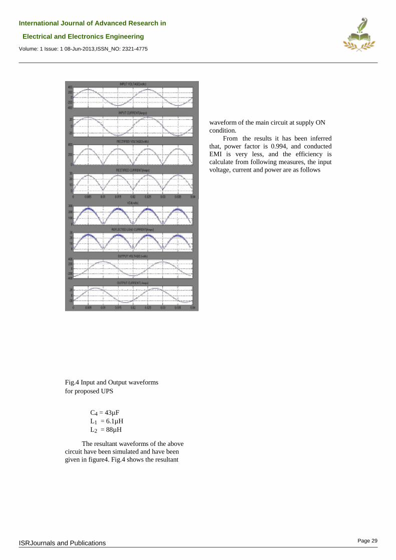
The design parameter values of the
above circuit are
C1 = 1µF C2 = 220nF C3 = 220nF
ISRJournals and Publications Page 28
International Journal of Advanced Research in
Electrical and Electronics Engineering
Volume: 1 Issue: 1 08-Jun-2013,ISSN_NO: 2321-4775
waveform of the main circuit at supply ON
condition.
From the results it has been inferred
that, power factor is 0.994, and conducted
EMI is very less, and the efficiency is
calculate from following measures, the input
voltage, current and power are as follows
Fig.4 Input and Output waveforms
for proposed UPS
C4 = 43µF
L1 = 6.1µH
L2 = 88µH
The resultant waveforms of the above
circuit have been simulated and have been
given in figure4. Fig.4 shows the resultant
ISRJournals and Publications Page 29
International Journal of Advanced Research in
Electrical and Electronics Engineering
Volume: 1 Issue: 1 08-Jun-2013,ISSN_NO: 2321-4775
Vin = 229.8 V
Iin = 17.78 A
Pin= 4080 W
7 Amps
Ild(t) - reflected load current in Amps
Icomp(t) - compensation current in Amps QPSRC -- charge of PSRC into C4 (C)
QCOMP -- charge of dynamic compensator
∆ Vc4 -- maximum output voltage ripple on C4 (V)
The output voltage, current and power
are as follows:
Vload=208 V
Iload=19.1 A Pload=3950 W
The efficiency of the entire
system under normal operating conditions
is measured as 96.2%.
VII. CONCLUSION
A new UPS configuration has been
described that features unity power factor,
transformer isolation through a high-
frequency link in the circuit. The concept
was developed for generating lower
conducted EMI, not only due to soft
switching, but containing the frequency
content of switching waveforms, particularly
those closed to the input and output of the
UPS. A single phase 230V, 50Hz, simulated
circuit, load up to 3.2kW, has been
presented, and measurements indicate the
low EMI is possible, and a Power Factor of
0.996 was measured, by simulated
waveforms in MATLAB software
NOMENCLATURE
Pout (t) - output power of the PSRC in watt
f - operating frequency of the PSRC in
Hertz
C4 -- output capacitance (F)
Cr - resonant capacitors (C2+C3) in
Farads
Vc1(t) - input across C1 in volts.
IPSRC(t) - output current of the PSRC in
ISRJournals and Publications Page 30

International Journal of Advanced Research in
Electrical and Electronics Engineering
Volume: 1 Issue: 1 08-Jun-2013,ISSN_NO: 2321-4775
VC4 -- peak overshoot voltage across C4 in volts
Itrans -- amplitude of inductor current to be
reversed in Amps
L2 -- value of inductor in Henry
tr -- the resonant current reversal period
in seconds.
V1 - the fundamental frequency rms value of the output voltage
Vh -- the rms magnitude at harmonic of order h.
REFERENCES [1] Widodo Sulistyono, Prasad Enjeti, “A Series
Resonant AC to DC Rectifier with High-
Frequency Isolation”, Proc.of pwercon.,Vol.10.
1995pp.1-7. . [2] Marinus Berg and Jan Ferreira, , “ A Family of
Low-EMI Unity Power Factor Converters” ,
IEEE Tans, Power Elect., Vol.13.No.3, May
1998pp.547-555
[3] F.Kamran and G.Habetler, October 1995, “ A
Novel On-line Uninterruptible Power Supply
with Universe Filtering Capabilities”, IEEE
Trans., Power Elect.,Vol.13.No.3, pp.410-418.
[4] Philip C.Theron and Jan Ferreira, ,” The Zero
Voltage Switching Partial Series Resonant
Converter”, IEEE Trans, Ind.Appl., Vol.31.No.4,
August 1995pp.879-886
[5] De Rooij and Jan Ferreira, “A Novel Unity
Power Factor Low-EMI Uninterruptible Power
Supply”, IEEE Trans, Ind.Appl., Vol.34.No.4,
August 1998,pp.870-876.
[6] Fred C.Lee, , “High Frequency Quasi-Resonant
Converter Techlogies”, IEEE
Proceedinngs, Vol.76.No.4 April 1988,
pp.377-389.
ISRJournals and Publications Page 31

International Journal of Advanced Research in
Electrical and Electronics Engineering
Volume: 1 Issue: 1 08-Jun-2013,ISSN_NO: 2321-4775
8
[7] Mohan, Undeland and Robbins, ,” Power
Electronics”, John Wiley& Sons, New
York,2001
[8] Chang Wu and Hurng Jou, ,” A New
Uninterruptible Power Supply Scheme
provides Harmonic Suppression and Input
Power Factor Correction”, IEEE Trans.,
Ind.Elect., Vol.42.No.6., December
1995,pp.629-635.
[9] Chang Wu and Hurng Jou, ,” A New
Uninterruptible Power Supply Scheme
provides Harmonic Suppression and Input
Power Factor Correction”, IEEE Trans.,
Ind.Elect., Vol.42.No.6., December
1995,pp.629-635.
[10] www.mathworks.com
Powered by TCPDF (www.tcpdf.org)
ISRJournals and Publications Page 32