Embed Size (px)
Citation preview

ARTICLE IN PRESS
Nuclear Instruments and Methods in Physics Research A 605 (2009) 293–300
Contents lists available at ScienceDirect
Nuclear Instruments and Methods inPhysics Research A
0168-90
doi:10.1
� Corr
Dodeca
E-m1 In
journal homepage: www.elsevier.com/locate/nima
A new multianodic large area photomultiplier to be used in underwaterneutrino detectors
S. Aiello a, A. Amore b, M. Anghinolfi c, M. Battaglieri c, A. Bersani d,c, M. Brunoldi d, L. Caponetto a,R. De Vita c, K. Fratini c, A. Grimaldi a, V. Kulikovskiy e, E. Leonora a, D. Lo Presti b,a, G. Mini d,S. Minutoli c, P. Musico c, M. Osipenko c, G. Ottonello c, D. Piombo c, N. Randazzo a, G. Ricco d,c,M. Ripani c, A. Rottura c, G.V. Russo b,a, A. Savasta b, D. Sciliberto a, E. Shirokov e, V. Sipala b,a,M. Taiuti d,c,�, S. Urso a, S. Zavatarelli c,1
a INFN Sezione Catania, Via S. Sofia 64, 95123 Catania, Italyb Dipartimento di Fisica e Astronomia, Universita di Catania, Via S. Sofia 64, 95123 Catania, Italyc INFN, sezione di Genova, Via Dodecaneso 33, I-16146 Genova, Italyd Dipartimento di Fisica dell’Universita di Genova, Via Dodecaneso 33, 16146 Genova, Italye Institute of Nuclear Physics, Moscow State University, 119899 Moscow, Russia
a r t i c l e i n f o
Article history:
Received 22 August 2008
Received in revised form
18 February 2009
Accepted 30 March 2009Available online 8 April 2009
Keywords:
Photomultiplier
Neutrino astronomy
Deep sea detector
02/$ - see front matter & 2009 Elsevier B.V. A
016/j.nima.2009.03.235
esponding author at: Dipartimento di Fisica d
neso 33, 16146 Genova, Italy. Tel.: +39 010 353
ail address: [email protected] (M. Taiuti
cooperation with the KM3NeT Consortium.
a b s t r a c t
In this article we describe the properties of a new 10-in. hemispherical photomultiplier manufactured
by Hamamatsu. The prototype has a segmented photocathode and four independent amplification
stages. The photomultiplier is one of the main components of a newly designed direction-sensitive
optical module to be employed in large-scale underwater neutrino telescopes. The R&D activity has
been co-funded by the INFN and the KM3NeT Consortium. The prototype performance fully meets with
the design specifications.
& 2009 Elsevier B.V. All rights reserved.
1. Introduction
One important component of an underwater neutrino tele-scope is the photodetector required to collect the Cherenkov lightproduced by the ionizing particles that originate from theinteraction of the neutrino [1–4]. To efficiently cover 1 km3
detection volume it would be necessary to deploy � 104
photomultipliers whose main requirements are a relatively largephotocathode area, high gain, low noise, low after pulse rate andgood timing resolution for single photon detection, the exactvalues depending on the detector design. The current minimumrequirements for such detectors, taken from the KM3NeTConceptual Design Report [5], are reported in Table 1.
The aim of the European KM3NeT [6] Consortium is to definethe Technical Design Report of the km3 detector to be deployed inthe Mediterranean Sea. Several new ideas are being developed to
ll rights reserved.
ell’Universita di Genova, Via
6203; fax: +39 010 313358.
).
improve the performance of the optical modules, e.g. theprototyping activity in progress at CERN [7], aimed at applyingthe ideas that originated the Philips ‘‘SMART’’ XP2600 [8] and thelater QUASAR-370 [9] to the production of a large area, high singlephoton resolution detector; or the work being carried on atNIKHEF with the idea of segmenting the photocathode area inorder to count the number of photons, by replacing a single 10-in.PMT with at least 12 3-in. PMTs [10].
Monte Carlo simulations show that if it were possible toidentify the Cherenkov light direction, reconstruction efficiencywould improve in particular for short tracks related to low energy(below 10 TeV) neutrinos or to tracks that partially cross thedetector. As an example, in Fig. 1 we report the effect of theinformation on the direction of the detected Cherenkov light onthe response of a km3 detector a la NEMO [12,13].
In the KM3NeT research framework we have proposed theimplementation of this feature by means of a multianodic 10-in.photomultiplier coupled to a light guide system so thatall the Cherenkov light arriving from the same direction isfocused on a well-defined sector of the photocathode. The basicworking principles have been discussed in Ref. [14]. Theconceptual design is based on a multi-anodic position sensitive

ARTICLE IN PRESS
2Log (E/GeV)
Effe
ctiv
e A
reas
Rat
io
1
1.2
1.4
1.6
1.8
2
2.2
2.4
2.5 3 3.5 4 4.5 5 5.5 6 6.5 7
Fig. 1. The ratio of the effective areas of the NEMO detector equipped with
direction-sensitive optical modules and the standard NEMO detector.
R
x
R
x
Fig. 2. Left: behaviour of the classical optical module: all the Cherenkov light
coming from a specific direction illuminates the whole photocathode surface.
Right: the mirrors concentrate the light coming from a specific direction onto a
single sector of the photocathode surface.
Fig. 3. The picture of the interior of the dark box with the moving system and the
photomultiplier with the mu-metal cage.
Table 1KM3NeT technologies detector requirements.
Time resolution (for a single photon,
photomultiplier + electronics)
o2 ns
Position resolution o40 cm
Charge dynamic range � 100=25 ns
Two-hit time separation o25 ns
Coincidence acceptance 450%
False coincidences Dominated by random coincidences from
marine background photons
Dark noise rate o20% of the 40K rate
Failure rate of the optical modules o10% over 10 years without major
maintenance
The table is taken from Ref. [5].
S. Aiello et al. / Nuclear Instruments and Methods in Physics Research A 605 (2009) 293–300294
10-in. photomultiplier coupled to a set of mirrors. The mirrors arerealized with 3M Radiant Mirror Films glued onto 2 mm Plexiglasfoils. The 3M films are multi-layer polymeric films with areflectivity larger than 95% in the wavelength interval400–700 nm [15]. Fig. 2 shows how the side view of the opticalmodule changes with the mirrors: all photons arriving from thesame direction are focused by the mirror system onto a singlesector of the multi-anodic photomultiplier. In this way the angularacceptance of the optical module is divided into four with only asmall overlap along the symmetry axis of the photomultiplier. The
result is greater accuracy in the evaluation of the direction of thedetected light is increased.
Large area multianodic photomultipliers are not commerciallyavailable and, therefore, we contacted the leading companiesin the field in order to investigate the feasibility of producingsuch a device. In this paper we present the performances ofthe two prototypes of a 10-in. 4-anodic photomultiplier manu-factured by Hamamatsu. The two samples (ZF0021 and ZF0025)are of the same shape as the 10-in. Hamamatsu R7081. Likethe Hamamatsu R7081, the amplification chain includes 10dynode stages. The photomultiplier hosts four separatedynode chains with common voltages. To perform the teststhe photomultiplier was connected to a resistive voltagedivider produced according to the specifications provided byHamamatsu.
2. Testing facility
The testing facility used to measure the characteristicsof the large area photomultipliers is based on a light-tightdark box, with dimensions 2:0� 1:7� 1:5 m3, equipped with aframe designed to host the photomultiplier, a moving systemrequired to scan the photocathode surface with the lightsource and a PMT used as a monitor to check the stability of thelight source. The light source, located outside, is a 410 nmPICOQUANT pulsed laser [16], with a pulse width of 60 ps, wholefrequency can vary in the range of 0–40 MHz using an externalgenerator. For a precise calibration of the source in singlephotoelectron condition, we used a DEP Hybrid PhotoDiodePP0270K. The laser optical power range was calibrated using tanOPHIR PD-300 bolometer [17], to measure the linearity of thephototube.
The light pulses are brought into the dark box by a 50mmmultimode optical fibre, and then split into two fibres toilluminate the PMT under test and the reference PMT. Inorder to study the characteristics of the photomultiplier’sresponse locally, the fibre is mounted on a moving systemthat allows the entire photocathode area to be scanned with a5 mm diameter single-photon pulsed beam. The moving systemis constituted by a semicircular guide capable of rotatingvertically in the angular interval 0–1801 and a frame holding theoptical fibre that can move from one extremity of the guide to the

ARTICLE IN PRESS
S. Aiello et al. / Nuclear Instruments and Methods in Physics Research A 605 (2009) 293–300 295
other. The movement of the two elements, obtained with twoindependent motors controlled by a PC, allows the wholehemispherical photocathode surface to be scanned with theextremity of the optical fibre continually pointing toward thecentre of the semicircular guide. A picture of the interior ofthe dark box is shown in Fig. 3.
A custom software developed in LabView controls thesequence of all the operations, in particular the source movementand the data acquisition. On the basis of the geometriccharacteristics of the PMT, the software calculates the distributionof the measured points on the photocathode surface, making it
HV [V]1400
Gai
n [#
] 108
A1A2A3A4
1450 1500 1550 1600 1650 1700 1750 1800
Fig. 4. The gain for each anode of the ZF0021 as a function of the applied HV. The
behaviour of A1 and A2 is almost the same and the points overlap.
Table 2Summary of the ZF0021 photomultiplier gain properties according to the power
law G ¼ G0 þ G1 � ðHV ½V �=1400Þm.
Anode A1 A2 A3 A4
G0 [�107] 0.04 0.85 0.00 0.19
G1 [�107] 3.5 3.0 3.8 2.5
m 7.23 7.83 7.66 7.63
Fig. 5. Typical single photon pulse shape distribution.
possible to choose the number of points and the angular step ofthe scan.
A more detailed description of the testing facility and of themeasurements reported in this paper can be found in Refs. [18,19].
3. Prototype performances
3.1. PMT gain
The gain of the photomultiplier was measured by studying thechange in position of the single-photon peak for each anode as afunction of the HV value using a calibrated charge ADC. The resultfor the ZF0021 sample is presented in Fig. 4: the experimentalpoints have been fitted using the power law G ¼ G0 þ G1�
ðHV ½V �=1400Þm. Three anodes (A1, A2 and A3 according to theHamamatsu numbering) behave similarly; the fourth anode A4has a smaller gain (� �25% at 1500 V). The dependence on the HVvalue is approximately the same. The parameters of the fit forsample ZF0021 are given in Table 2. Similar behaviour wasobserved with the ZF0025 where the A4 anode shows a gain �20% smaller. According to Hamamatsu this common behaviour isaccidental and is related to the quality of the dynodes [20].
The typical single photon pulse shape distribution is reportedin Fig. 5.
3.2. Overall response
In this section we report the response of the photomultiplierwhen the whole photocathode surface was uniformly illuminatedwith a plane-wave pulsed beam. The applied voltage was 1550 Vcorresponding to a nominal gain of � 5� 107. All measurementswere performed at room temperature. To entirely illuminate thephotocathode with a plane-wave pulsed beam the photomulti-plier was positioned away from the light source, at a calibrateddistance of 0.70 m.
The linearity was measured for each anode separately. Eachanode shows rather good linearity up to 100 photoelectrons asshown in Fig. 6 for anode A1 in the ZF0025 sample.
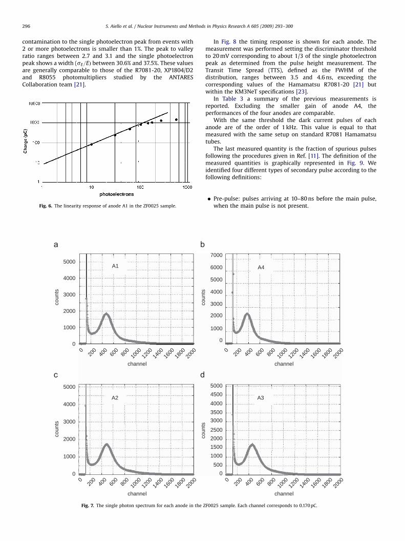
In Fig. 7 the pulse height is shown for each anode in theZF0025 sample when illuminated with a flux such that the
Each division on the x axis corresponds to 20 ns.
ARTICLE IN PRESS
S. Aiello et al. / Nuclear Instruments and Methods in Physics Research A 605 (2009) 293–300296
contamination to the single photoelectron peak from events with2 or more photoelectrons is smaller than 1%. The peak to valleyratio ranges between 2.7 and 3.1 and the single photoelectronpeak shows a width (sE=EÞ between 30.6% and 37.5%. These valuesare generally comparable to those of the R7081-20, XP1804/D2and R8055 photomultipliers studied by the ANTARESCollaboration team [21].
Fig. 6. The linearity response of anode A1 in the ZF0025 sample.
A1
A2
coun
tsco
unts
channel
channel
5000
4000
3000
2000
1000
5000
4000
3000
2000
1000
0
2000
1800
1600
1400
1200
100080
060
040
020
00
2000
1800
1600
1400
1200
100080
060
040
020
000
Fig. 7. The single photon spectrum for each anode in the Z
In Fig. 8 the timing response is shown for each anode. Themeasurement was performed setting the discriminator thresholdto 20 mV corresponding to about 1/3 of the single photoelectronpeak as determined from the pulse height measurement. TheTransit Time Spread (TTS), defined as the FWHM of thedistribution, ranges between 3.5 and 4.6 ns, exceeding thecorresponding values of the Hamamatsu R7081-20 [21] butwithin the KM3NeT specifications [23].
In Table 3 a summary of the previous measurements isreported. Excluding the smaller gain of anode A4, theperformances of the four anodes are comparable.
With the same threshold the dark current pulses of eachanode are of the order of 1 kHz. This value is equal to thatmeasured with the same setup on standard R7081 Hamamatsutubes.
The last measured quantity is the fraction of spurious pulsesfollowing the procedures given in Ref. [11]. The definition of themeasured quantities is graphically represented in Fig. 9. Weidentified four different types of secondary pulse according to thefollowing definitions:
�
counts
coun
ts
5
4
3
2
1
7
6
5
4
3
2
1
4
3
2
1
F00
Pre-pulse: pulses arriving at 10–80 ns before the main pulse,when the main pulse is not present.
A4
A3
channel
channel
000
000
000
000
000
000
000
000
000
000
000
000
0
500
500
500
500
500
2000
1800
1600
1400
1200
100080
060
040
020
00
2000
1800
1600
1400
1200
100080
060
040
020
00
0
25 sample. Each channel corresponds to 0.170 pC.

ARTICLE IN PRESS
A1
A2
A4
A3
channel8000700060005000400030002000
channel8000700060005000400030002000
channel8000700060005000400030002000
channel8000700060005000400030002000
coun
ts
4000
3000
2000
1000
0
4500
3500
2500
1500
500
coun
ts
5000
4000
3000
2000
1000
0
4500
3500
2500
1500
500
coun
ts
4000
3000
2000
1000
0
4500
3500
2500
1500
500
coun
ts
5000
4000
3000
2000
1000
0
Fig. 8. The timing distribution of the single photon for each anode in the ZF0025 sample. Each channel corresponds to 25 ps.
Table 3Summary of the ZF0025 photomultiplier properties at a HV of 1550 V.
Anode A1 A2 A3 A4
P=V 3.03 3.09 2.95 2.75
Gain [�107] 5.0 5.4 5.0 3.9
RSE (%) (sigma) 33.6 30.6 37.3 35.2
TT (ns) 105 106 106 105
TTS (ns) (FWHM) 4.6 4.0 3.5 4.2
Fig. 9. The adopted definition of pre- and after pulses.
0 1000 2000 3000 4000 5000 6000 7000 8000 9000Ch TAC
even
ts
0
2
10
12
14
8
6
4
Range TAC = 200 ns
After pulses type 1 = 1.569%
Fig. 10. The time distribution of the Type 1 After pulse for anode A1 in the ZF0025
sample.
S. Aiello et al. / Nuclear Instruments and Methods in Physics Research A 605 (2009) 293–300 297
�
Late pulse: pulses arriving at 10–80 ns after the main pulse,when the main pulse is not present. � After pulse 1: spurious pulses arriving at 10–80 ns after themain pulse.
�
After pulse 2: spurious pulses arriving at 80 ns–16ms after themain pulse.Late pulses and After pulses 1 differ in that the former arebelieved to arise from photoelectron backscattering on the first

ARTICLE IN PRESS
0 1000 2000 3000 4000 5000 6000 7000 8000 9000Ch TAC
even
ts
0
10
50
60
70
80
40
30
20
range TAC = 20 us
after pulses type 2 = 10.873%
Fig. 11. The time distribution of the Type 2 After pulse for anode A1 in the ZF0025
sample.
Table 4Summary of spurious pulses for sample ZF0025.
Anode A1 A2 A3 A4
Pre-pulses (%) 0.05 0.18 0.24 0.05
Late pulses (%) 7.74 7.96 7.14 6.50
After pulses 1 (%) 1.57 1.91 1.68 1.22
After pulses 2 (%) 10.87 12.53 13.49 10.41
Fig. 12. The reference system adopted in the measurements. In the top-right the
hemispherical surface of the photocathode is shown: the photomultiplier is
aligned along the y-axis and the top of the photocathode corresponds to y ¼ 90�
and f ¼ 90� . The circle represents the shape of the photomultiplier as seen from a
point along the y-axis. The correspondence between the angles and the four
anodes is also shown.
S. Aiello et al. / Nuclear Instruments and Methods in Physics Research A 605 (2009) 293–300298
dynodes, and the latter are believed to originate from theionization of the residual gas atoms and the atoms adsorbed bythe first dynode surface.
A typical distribution of After pulses 1 and 2 is reported inFigs. 10 and 11, respectively. A summary of the spurious pulses is givenin Table 4. The values represent the ratio of the number of spuriouspulses to the number of main pulses, expressed as percentages.
3.3. The local response
To be used in a direction-sensitive optical module the multi-anodic photomultiplier should be able to identify precisely theposition of the photocathode emission point. Therefore theresponse of the photomultiplier was studied for each anodeindividually, by illuminating the photocathode area with a single-photon pulsed beam with 5 mm-diameter. A scan of the photo-cathode surface was performed using a 324-points grid.
The angle definition adopted to represent the results is shownin Fig. 12. In Fig. 13 the area of the single photon peak is reportedfor each anode. The area includes all the events with a chargecorresponding to more than 1/3 photoelectrons. The largestmeasured values are represented in red and the smallest, equalto less than 2% of the largest measured value, in blue. Comparingthe response of the four anodes it is evident that each anode issensitive to approximately one-fourth of the photocathode areawith small differences in the shape of the transition regionbetween the various quarters.
In Fig. 13 it can also be observed that each anode shows aresidual sensitivity (in the order of few %) to the remainingphotocathode area. This could affect the performance of thedirection-sensitive optical module. Therefore we investigated theorigin of the effect in more detail using the oscilloscope tomonitor the shape of the four anode signals when the centre ofthe photocathode sector connected to anode A1 is illuminated. InFig. 14 the shape of the signals is reported. The effect is shown fora laser intensity corresponding to an average of 15 photo-electrons, but it is the same for the whole dynamic rangestudied. The figure shows that, in coincidence with the regularunipolar signal, the coupling between the dynodic chainsgenerates three oscillating parasitic outputs. The parasiticsignals have amplitudes of approximately 16% of the regularsignal and a charge � 3% of the good one. Therefore the residualsensitivity that appears in Fig. 13 is largely related to thoseparasitic signals that exceed the thresholds of the acquisitionsystem. We expect to reduce the cross-talk by analysing thedifferent shapes of the parasitic signals and work is currently inprogress on the design of an electronic board dedicated to thistask.
It is worth noting that if the measurements reported in Fig. 13are compared with the typical surface of the standard photo-cathode as reported in Fig. 15 the result is that the effectivephotocathode area extends up to the geometrical limit of thephotomultiplier hemisphere, while the standard 10-in.photomultiplier shows a reduced surface. From purelygeometrical considerations we have estimated that theprototype could collect up to 20% more light.
We are presently developing an optical module equipped withthe 4-anodic prototype in order to measure how the directionalityand the larger sensitive area could improve the performance ofthis device. The results will be reported and discussed in a furtherpaper.
4. Conclusions
We tested two prototypes of a large area (10-in.) hemisphericalmultianodic photomultiplier manufactured by Hamamatsu. Themeasurements show good linearity up to 100 photoelectrons, again higher than 107 and a gain uniformity better than 10% with

ARTICLE IN PRESS
Fig. 13. The local response of the photocathode to a single photoelectron for each anode of the ZF0025 prototype.
Fig. 14. The effect of the coupling between the four ZF0025 dynodic chains. C1 represents the active anode. C2, C3 and C4 are plotted in a �10 expanded scale to enhance
the effect. Each division on the x axis corresponds to 10 ns.
S. Aiello et al. / Nuclear Instruments and Methods in Physics Research A 605 (2009) 293–300 299
only one anode that differs by � 25% due to the quality of thedynodes. The prototype performances are fully in line with theKM3NeT specification. By scanning the photocathode surface witha thin light beam we verified that there is less than 3% cross-talkbetween the prototype anodes. The cross-talk is mainly generated
by the capacitive coupling of the four dynodic chains and could befurther reduced with a pulse shape analysis using a dedicatedelectronics. Finally the shape of the first dynode allows thephotocathode surface to be enlarged providing 20% more collectedlight compared to a standard Hamamatsu 10-in. photomultiplier.

ARTICLE IN PRESS
�220 MIN.
245±
530
5 M
AX
.
20 PIN BASEJEDEC No. B20-102
R136.7
�84.5±2.0
�253±5
φ = 0° φ =180°
Fig. 15. The section of the Hamamatsu photomultiplier at y ¼ 90�. The dashed line
represents the typical coverage of the photocathode for the standard 10-in. The
points corresponding to f ¼ 0� and 180� are also shown. The drawing has been
taken from Hamamatsu data sheets [22]. The meaning of y and f is given in Fig. 12.
S. Aiello et al. / Nuclear Instruments and Methods in Physics Research A 605 (2009) 293–300300
Acknowledgements
The authors wish to thank Hamamatsu Photonics for their helpin producing the prototypes of the multianodic large area
photomultiplier. This work was supported in part by the ItalianIstituto Nazionale di Fisica Nucleare and the KM3NeT DesignStudy, funded by the EU through FP6, Contract no. 11937.
References
[1] P. Amram, et al., ANTARES Collaboration, Nucl. Instr. and Meth. A 484 (2002)369 [arXiv:astro-ph/0112172].
[2] K. Hanson, O. Tarasova, IceCube Collaboration, Nucl. Instr. and Meth. A 567(2006) 214.
[3] R.I. Bagduev, et al., Nucl. Instr. and Meth. A 420 (1999) 138 [arXiv:astro-ph/9903347].
[4] E.G. Anassontzis, et al., NESTOR Collaboration, Nucl. Instr. and Meth. A 479(2002) 439.
[5] hhttp://www.km3net.org/CDR/CDR-KM3NeT.pdfi.[6] hhttp://www.km3net.orgi.[7] A. Braem, C. Joram, J. Seguinot, P. Lavoute, C. Moussant, Nucl. Instr. and Meth.
A 570 (2007) 467.[8] P.C. Bosetti, An Optical Sensor for DUMAND II, Proc. 23rd ICRC (Calgary), vol.
4, 1993, p. 534.[9] B.K. Lubsandorzhev, BAIKAL and TUNKA Collaboration, Nucl. Instr. and Meth.
A 442 (2000) 368.[10] P. Kooijman, Nucl. Instr. and Meth. A 567 (2006) 508.[11] B.K. Lubsandorzhiev, R.V. Vasiliev, Y.E. Vyatchin, B.A.J. Shaibonov, Nucl. Instr.
and Meth. A 567 (2006) 12 [arXiv:physics/0601157].[12] E. Migneco, et al., Nucl. Instr. and Meth. A 567 (2006) 444.[13] M. Anghinolfi, et al. INFN Note INFN-TC-08-2, available at hhttp://
www.lnf.infn.it/sis/preprint/i, 2008.[14] M. Taiuti, Nucl. Instr. and Meth. A 525 (2004) 137.[15] M. Brunoldi, et al., INFN Note INFN-TC-07-9, available at hhttp://www.lnf.infn.
it/sis/preprint/i, 2007.[16] hhttp://www.picoquant.com/i.[17] hhttp://www.ophiropt.com/i.[18] A. Savasta, Thesis, Universitiy of Catania (in Italian), 2007.[19] E. Leonora, Nucl. Instr. and Meth. A 602 (2009) 217.[20] Private communication.[21] J.A. Aguilar, et al., ANTARES Collaboration, Nucl. Instr. and Meth. A 555 (2005)
132 [arXiv:physics/0510031].[22] Photomultiplier tubes and assembly for scintillation counting & high energy
physics, Hamamatsu catalog.[23] KM3NeT conceptual design report for a deep-sea research infrastructure
incorporating a very large volume neutrino telescope in the mediterraneansea hhttp://www.km3net.org/design.phpi.