Embed Size (px)
Citation preview

A Motorola MC68008 Op-codecompatible VHDL Microprocessor
David LynchSN : 00019640
Supervisor : Michael ManzkeB.A (Mod) Computer Science Final Year Project
April, 2004

Abstract
The goal of this project is to implement a Motorola 68008 op-code compatible mi-croprocessor capable of functioning on an FPGA. The CPU is to be specified fully inVHDL and is designed to emulate the functionality of the MC68008 in terms of in-struction set decoding, operand addressing and bus operation. The ultimate targetdevice is a custom designed FPGA-Board used in education of Computer Scienceand Engineering Students in TCD. As a result of this a large emphasis has beenplaced on structured, correct design flow and specification as well as readability ofthe code.

Acknowledgments
I would like to thank Michael Manzke, my project supervisor for all the help andsupport given throughout the project. Appreciation is also extended to Ross Bren-nan for support on his FPGA board and bus-interfacing. Lastly I would like tothank John McCarthy, my Integrated Systems Design lecturer for help in masteringthe use of the Xilinx platform and companion tools.1.
1This document has been typeset using LATEX
i

Contents
1 Introduction 11.1 Current Project . . . . . . . . . . . . . . . . . . . . . . . . . . . . . . 1
1.1.1 Computer Architecture Coursework . . . . . . . . . . . . . . 11.1.2 The FPGA Design . . . . . . . . . . . . . . . . . . . . . . . . 4
1.2 Motivation . . . . . . . . . . . . . . . . . . . . . . . . . . . . . . . . . 61.3 Design Approach . . . . . . . . . . . . . . . . . . . . . . . . . . . . . 7
1.3.1 VHDL Programming . . . . . . . . . . . . . . . . . . . . . . . 81.4 Motorola 68000 Microrocessor Overview . . . . . . . . . . . . . . . . 9
2 Hardware Design 132.1 Overview . . . . . . . . . . . . . . . . . . . . . . . . . . . . . . . . . . 132.2 Functional Unit . . . . . . . . . . . . . . . . . . . . . . . . . . . . . . 14
2.2.1 The Arithmetic and Logic Unit . . . . . . . . . . . . . . . . . 152.2.2 The Shifter . . . . . . . . . . . . . . . . . . . . . . . . . . . . 182.2.3 Control Registers . . . . . . . . . . . . . . . . . . . . . . . . . 19
2.3 Data Storage and Movement . . . . . . . . . . . . . . . . . . . . . . . 212.3.1 Register File . . . . . . . . . . . . . . . . . . . . . . . . . . . . 212.3.2 Data Bus and Address Bus Selection . . . . . . . . . . . . . . 232.3.3 The IPL control Module . . . . . . . . . . . . . . . . . . . . . 24
2.4 The Bus Interface . . . . . . . . . . . . . . . . . . . . . . . . . . . . . 242.4.1 Implementation . . . . . . . . . . . . . . . . . . . . . . . . . . 252.4.2 Read and Write Cycles . . . . . . . . . . . . . . . . . . . . . . 262.4.3 Interrupt Acknowledge and Bus Error Cycles . . . . . . . . . . 272.4.4 Bus Interface Hardware . . . . . . . . . . . . . . . . . . . . . 30
2.5 Sequencing and Control . . . . . . . . . . . . . . . . . . . . . . . . . 302.5.1 Control Path Registers . . . . . . . . . . . . . . . . . . . . . . 312.5.2 Micro-sequencing . . . . . . . . . . . . . . . . . . . . . . . . . 322.5.3 Instruction Decoding . . . . . . . . . . . . . . . . . . . . . . . 362.5.4 The Control Word . . . . . . . . . . . . . . . . . . . . . . . . 39
3 Micro-programming the design 423.1 Control Word Generation . . . . . . . . . . . . . . . . . . . . . . . . 423.2 System Control Programming . . . . . . . . . . . . . . . . . . . . . . 43
3.2.1 Memory Access . . . . . . . . . . . . . . . . . . . . . . . . . . 433.2.2 RESET Handler . . . . . . . . . . . . . . . . . . . . . . . . . . 443.2.3 Fetch-Decode-Execute Sequence . . . . . . . . . . . . . . . . . 45
ii

3.3 The MOVE instruction . . . . . . . . . . . . . . . . . . . . . . . . . . 463.3.1 Decoding . . . . . . . . . . . . . . . . . . . . . . . . . . . . . 463.3.2 Fetch using Addressing Modes . . . . . . . . . . . . . . . . . . 473.3.3 Write Back . . . . . . . . . . . . . . . . . . . . . . . . . . . . 47
3.4 The MULU instruction . . . . . . . . . . . . . . . . . . . . . . . . . . 483.4.1 The Shift-and-Add Algorithm . . . . . . . . . . . . . . . . . . 483.4.2 Other Instructions . . . . . . . . . . . . . . . . . . . . . . . . 49
4 Testing and Conclusions 504.1 Design Testing and Development Progress . . . . . . . . . . . . . . . 50
4.1.1 Synthesis . . . . . . . . . . . . . . . . . . . . . . . . . . . . . 514.1.2 A 68008 demonstration . . . . . . . . . . . . . . . . . . . . . . 52
4.2 Conclusions . . . . . . . . . . . . . . . . . . . . . . . . . . . . . . . . 554.2.1 Skills Acquired and Lessons Learned . . . . . . . . . . . . . . 564.2.2 Further Work . . . . . . . . . . . . . . . . . . . . . . . . . . . 57
Bibliography 57
Appendix A, CWORD Guide 59
Appendix B, Design Hierarchy 62
iii

List of Figures
1.1 The 68008 package . . . . . . . . . . . . . . . . . . . . . . . . . . . . 21.2 The Leon Core. Source : ESA[5] . . . . . . . . . . . . . . . . . . . . . 51.3 The 68000 System Register . . . . . . . . . . . . . . . . . . . . . . . . 10
2.1 Functional Unit Block Diagram . . . . . . . . . . . . . . . . . . . . . 142.2 ALU Block Diagram . . . . . . . . . . . . . . . . . . . . . . . . . . . 162.3 BIN control CSA. BIN Feeds the Y input of the adder array . . . . . 172.4 68000 Shifting. Source : MC68000 Programmers Reference . . . . . . 182.5 VHDL Rotate Right using case for combinatorial logic . . . . . . . . 192.6 The System Register . . . . . . . . . . . . . . . . . . . . . . . . . . . 202.7 Register File and Control . . . . . . . . . . . . . . . . . . . . . . . . . 222.8 Bus Interface Block Diagram . . . . . . . . . . . . . . . . . . . . . . . 252.9 Sample Read Operation State flow (Simplified) . . . . . . . . . . . . . 262.10 Setting outputs for the idle state . . . . . . . . . . . . . . . . . . . . 272.11 Bus Read Cycle . . . . . . . . . . . . . . . . . . . . . . . . . . . . . . 282.12 Bus Write Cycle . . . . . . . . . . . . . . . . . . . . . . . . . . . . . . 282.13 Auto-vector peripheral bus cycle . . . . . . . . . . . . . . . . . . . . . 292.14 CROM and Control Address Register . . . . . . . . . . . . . . . . . . 302.15 Microsequencer Block Diagram . . . . . . . . . . . . . . . . . . . . . 322.16 Micro-Branching Flow . . . . . . . . . . . . . . . . . . . . . . . . . . 342.17 Effective Address Field . . . . . . . . . . . . . . . . . . . . . . . . . . 372.18 MOVE.B #5,(A0) Instruction . . . . . . . . . . . . . . . . . . . . . . 372.19 Instruction encoding for group 0000 . . . . . . . . . . . . . . . . . . . 382.20 Instruction Decoder and mapping ROM . . . . . . . . . . . . . . . . 392.21 CWORD Formats . . . . . . . . . . . . . . . . . . . . . . . . . . . . . 40
3.1 Generating a CWORD to Add D0 to D1 . . . . . . . . . . . . . . . . 433.2 The Fetch-Decode-Execute Cycle . . . . . . . . . . . . . . . . . . . . 453.3 MOVE Instruction Form . . . . . . . . . . . . . . . . . . . . . . . . 46
4.1 The Virtual Board Simulation Setup . . . . . . . . . . . . . . . . . . 524.2 Multiplication of 2D Matrices . . . . . . . . . . . . . . . . . . . . . . 524.3 A timing diagram for the first 9ns of operation . . . . . . . . . . . . . 544.4 The final write back . . . . . . . . . . . . . . . . . . . . . . . . . . . 554.5 RAM contents after the program has finished . . . . . . . . . . . . . 56
iv

List of Tables
1.1 68k Pin Description . . . . . . . . . . . . . . . . . . . . . . . . . . . . 21.2 Addressing Modes [1] . . . . . . . . . . . . . . . . . . . . . . . . . . . 101.3 Data Transfer Instructions [1] . . . . . . . . . . . . . . . . . . . . . . 111.4 Program Flow Control Instructions . . . . . . . . . . . . . . . . . . . 11
2.1 Functional Unit Operation Select . . . . . . . . . . . . . . . . . . . . 152.2 SR Load Control . . . . . . . . . . . . . . . . . . . . . . . . . . . . . 212.3 Internal Register Map . . . . . . . . . . . . . . . . . . . . . . . . . . 222.4 Destination and Source Selection in the Register File . . . . . . . . . 232.5 BI Select . . . . . . . . . . . . . . . . . . . . . . . . . . . . . . . . . . 292.6 MCA Selection . . . . . . . . . . . . . . . . . . . . . . . . . . . . . . 332.7 CCOND Possible Branching Conditions and CCR Codes . . . . . . . 352.8 Decoding an EA . . . . . . . . . . . . . . . . . . . . . . . . . . . . . . 372.9 CWORD Field Function . . . . . . . . . . . . . . . . . . . . . . . . . 41
3.1 Memory Access CROM Locations . . . . . . . . . . . . . . . . . . . . 43
v

Chapter 1
Introduction
This chapter serves as an introduction to the Motorola 68008 VHDL1 CPU project.The background and motivations behind such a project are outlined. In doing so,current project-board design is introduced along with the improved board designas proposed and implemented by Ross Brennan, together with arguments for thecontinued use of the MC68008 in an educational context. This chapter also exploresthe design approach taken and reasons for such an approach.
1.1 Current Project
This project branches directly from the final year project completed by Ross Bren-nan entitled, The Design and Evaluation of an FPGA based Microprocessor ProjectBoard [2]. The core objective of Brennan‘s project was to explore the possibil-ity and feasibility of introducing configurable hardware devices into Architecturecourses taken by Computer Science students and Computer Engineering Studentswith a view to upgrading the project system-boards to take advantage of recenthardware advances.
1.1.1 Computer Architecture Coursework
As a coursework section in the Computer Architecture I module of the B.A. (Mod)Computer Science degree at TCD. Students are required to build a functioningmicroprocessor system using core components. By completing such a project stu-dents become acquainted with the fundamentals of CPU-to-peripheral interaction,bus operation, asynchronous communication and board-level programming. Theproject is centred on the Motorola MC68008 processor with which students are re-quired to interface two 8k static RAM chips, an 8k EEPROM and a Rockwell R6551Asynchronous communications adapter. Wire wrap is used to connect the devicestogether after they have been placed on a purpose built system board.
The MC68008 processor is a 16-bit CISC2 design released in late 1982 as areplica of the MC68000 except with a reduced data-bus width of 8-bits. This reduc-tion was implemented in order to preserve compatibility with legacy 8-bit devices.
1Very High Speed Integrated Circuit Hardware Description Language2Complex Instruction Set Computer
1

As an early CISC computer the 68000 strikes a nice balance between a powerfulinstruction set, advanced memory addressing capability and simplicity of interface.Largely due to the absence of legacy instruction support, floating point arithmetic,or multi-media extensions commonly found in todays processors, this balance is verydesirable in an educational context, particularly when introducing junior freshmenstudents to low-level programming.
The MC68008 possesses a 20-bit address bus, allowing 1MB of in total ad-dressable memory space. An 8-bit bi-directional data bus allows the MC68008 tocommunicate external on-board devices using asynchronous bus protocols definedby Motorola. The package is described in Fig. 1.1 and the pin functions detailed inTable 1.1.
Figure 1.1: The 68008 package
Pins Description FunctionA19 : A0 Address BusD7 : D0 Data Bus/DTACK Bus Read Acknowledge Asynchronous bus control
/AS Address-on-bus/DS Data StrobeR/W Read Write/VPA Valid Peripheral Address Peripheral Control
E Peripheral Clock Synchronisation/IPL[2:0] Interrupt Level External Interrupt Control/BERR Bus Error System Control/RESET Reset Signal/HALT Processor Halt/BR Bus Request Bus Arbitration Control/BG Bus Grant
Table 1.1: 68k Pin Description
2

Components Used
• 1 x Motorola MC68008 Microprocessor
• 1 x R6551 Serial Interface
• 1 x 2764 8k EPROM
• 2 x HM6116P 2Kx8-bit Static RAM
• miscellaneous components including A 7404 Hex Inverter, 7407 Hex Buffer,74LS73 J-K Flip Flops, Dual 4-bit binary counter and a resistor pack.
Students are given access to a pre-designed project board. This board has a5V power supply and a parallel interface for connection with a logic state analyser.A 14.7465Mhz Crystal Oscillator is also integrated to provide clock signals for theACIA3 and the MC68008. The board acts as a basis on which to place the 5V TTLpin packages supplied. Once placed in the pin-holders students use copper wire wrapto connect the pin packages together.
The project stages
• Verify the board is generating a 15MHz clock signal using an oscilloscope.
• Use the 4-bit counter and the resistor pack to generate an 8Mhz clock signalfor the MC68008 and a 1Mhz clock signal for the ACIAs.
• Use the hex-inverter package, and Schmitt triggers to create a debounce circuitwhich ensures the RESET signal is kept asserted for at least 3 clock cycles.This ensures correct reset of internal circuitry and the peripherals.
• Memory map the RAM chips, the EEPROM and the ACIA using the GAL4 togenerate appropriate chip-enable signals depending on the processor AddressStrobe (/AS), Data Strobe (/DS) and Address Bus (A19 : A0). The studentsuse PALASM to generate equations which are then programmed to the GALchip.
• Program the EEPROM to provide the processor with a means of testing thebus interface. A suggested approach is through repeated JMP instructionexecution.
• Establish and verify the functionality of the RAM. This can be done with asimilar loop to the above, with the additional use of the MOVE instruction totest the memory space where each of the RAM chips resides.
• Use the JK Flip flop package provided to generate correct VPA and IPL sig-nalling to enable the ACIA to operate as a peripheral component. Use thesesignals to provide an EEPROM program to handle interrupts generated by theACIA and create a transparent link with a PC using a hyper-terminal session.
3Asynchronous Communications Device4General Array Logic — A simple programmable device
3

• Upon successful completion of the above, the students are then asked to createa simple monitor program using the EEPROM and 68k Assembly language.
1.1.2 The FPGA Design
FPGA devices are re-programmable and offer unparalleled flexibility for hardwarespecification. With recent advances in re-programmable logic devices, such as de-creased FPGA device scale and increased speed as well as the evolution of synthesissoftware tools like Xilinx Foundation[13] it has become increasingly more feasible todevelop fully-specified CPUs within a programmable hardware paradigm. The opensource movement has seen a spiral in such core implementations.[4]
The advantages of using an FPGA implementation are numerous. The stu-dent is no longer only exposed to bus interfacing, but allowed to examine howsuch a device may be logically implemented using a hardware description language.Furthermore, the flexibility of the FPGA design allows students to compare andcontrast specific technologies. For example, the student may wish to switch off theon-chip cache of a microprocessor to measure performance, or, switch between aRISC and CISC CPU to use different instruction sets, all without having to re-wirethe microprocessor board set up. Lastly, an FPGA design could replace the 68008pin-packages which are obsolete in their current form and are becoming increasinglydifficult to replace.
Board Hardware
Ross Brennan prototyped a replacement project board that was centred on a XilinxVirtex-II XV1000-256 FPGA. As 1 Million Gate Device, this FPGA would provideample basis in which to situate a RISC HDL-CPU 5 as well as space for additionalstudent design or a second CPU. The RAM and GAL components used in theoriginal project are still used here, although adapted to LL3V voltage operation tosuit the Xilinx FPGA voltages6. A PROM has also been added to the design. Thisfeature allows on-board programming of the FPGA on power up. As the FPGA isbased on SRAM technology the programming is lost at power down. The PROMprovides a quick way to program the FPGA with a selected architecture withouthaving to connect the system to a synthesis tool. [2, R. Brennan]
When the HDL design is synthesized, a bit file is generated by the synthesistool. This is then downloaded onto the FPGA using an interface port. However,because the FPGA is based on SRAM, the programmed design is lost at power-down. The PROM remedies this by providing the FPGA with a bit file at power on.The PROM may also contain different designs, e.g. the bit-files for a RISC designand a MC68008 design allowing the user to change between the two without havingto synthesize and download a new design from scratch.
5The proposed RISC design would use 80% of these resources at full-specification6The original packages are 5V TTL
4

LEON CPU Core
The LEON[5] core is a fully featured SPARC V8[12] compatible Core specified inVHDL and developed by the European Space Agency. It has a 32-bit data bus,floating point units, on-chip caches and a memory control unit. This core was chosenbecause it is an OpenSource VHDL implementation that is highly configurable, thuslending itself to the ideal educational environment described above.
Figure 1.2: The Leon Core. Source : ESA[5]
In order for the LEON to suffice as a replacement for the MC68008 pin-packagemodifications were necessary. The main objective was to emulate the simplicityof MC68008 bus interaction and to ensure compatibility with the currently usedRAM, ROM and GAL devices. The LEON was cut down to those componentsonly necessary for the function of the CPU. Although the LEON is capable of a58Mhz clock speed [2, Brennan], an 8Mhz clock has been provided. Caches werealso removed from the design as caching would inhibit the ability of the student touse an oscilloscope and logic state analyser to monitor bus activity. If the executed
5

program, such as the JMP loop, was read from memory once, it would be cachedin one bus cycle. Subsequent bus cycles would not occur, thus causing difficultywhen testing for correct bus function. Likewise, The Memory Management unitwas removed. The internal UARTS also needed to be removed as interfacing anasynchronous communications device to the processor is a core requirement of theComputer Architecture project therefore use of internal serial communication isnot required. For the same reason, internal reset circuitry was removed. The LEONdata-bus was reduced to 8-bits, to preserve component compatibility. It is calculatedthat an approx 95% decrease in performance would result from the changes, howeverit is noted here that the result is not a disadvantage for the student. A functionalsystem is much more desirable than a fast system in and educational context. [2]
1.2 Motivation
There are several purposes to this project. The main purpose is to provide a VHDL68008 microprocessor for the above project board. As described by Brennan andManzke [3], a 68008 HDL CPU would provide students with a CPU on-which theycould learn assembly programming using a small, simple but powerful instructionset. More importantly once the processor had a bus interface capable of being usedon the existing project board, it opens possibilities for expanding FPGA based mi-croprocessor boards to allow users to configure various parts of the design to theirparticular needs and use different architectures within the same physical hardwareparadigm. The 68008 CPU could also help preserve the use of the Motorola pro-cessor as a teaching tool. It is currently heavily used in Computer Science andComputer Engineering hardware modules due to its simplicity when compared toother processors. However, as the processor ages, it has become more and moredifficult to obtain replacement 5VTLL packages when necessary. An FPGA designmay eventually be a cheaper and simpler way of maintaining 68000 resources withinthe college.
Also, a motivation is to provide students of Computer Architecture with anunderstandable implementation of a micro-programmed CISC architecture as im-plemented using VHDL. Currently, Junior Freshmen studying for the B.A. (Mod)are exposed to digital fundamentals such as adder design and multiplexer designusing primitive digital logic gates. Senior Freshmen are exposed to multiple-cycleCPU design and more complex primitives such as Arithmetic Logic Units (ALU).It would be very desirable for students of these courses to be able to break down aCPU implementation into its core components and examine the design. A VHDLdesign programmed in an efficient and modular manner allows a user to examinea core component, completely ignoring the surrounding implementation. Thereforestudents can not only see where a primitive component may be used, but also howsuch a primitive may be implemented using a hardware specification language.
6
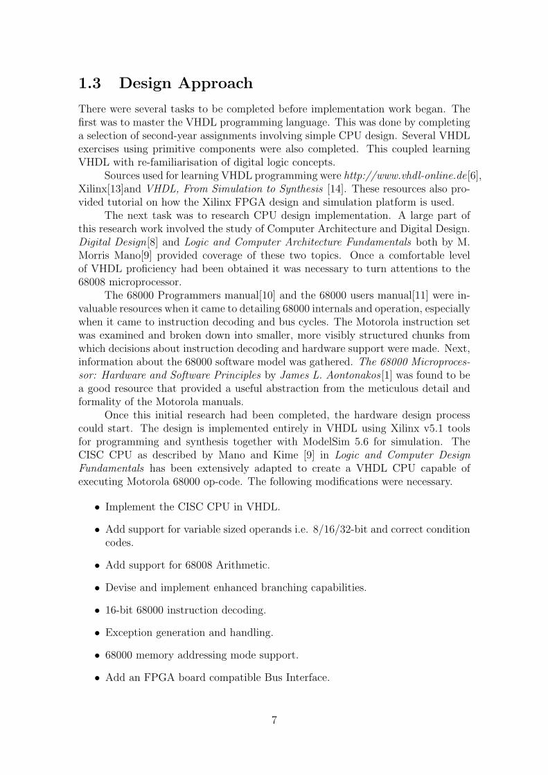
1.3 Design Approach
There were several tasks to be completed before implementation work began. Thefirst was to master the VHDL programming language. This was done by completinga selection of second-year assignments involving simple CPU design. Several VHDLexercises using primitive components were also completed. This coupled learningVHDL with re-familiarisation of digital logic concepts.
Sources used for learning VHDL programming were http://www.vhdl-online.de[6],Xilinx[13]and VHDL, From Simulation to Synthesis [14]. These resources also pro-vided tutorial on how the Xilinx FPGA design and simulation platform is used.
The next task was to research CPU design implementation. A large part ofthis research work involved the study of Computer Architecture and Digital Design.Digital Design[8] and Logic and Computer Architecture Fundamentals both by M.Morris Mano[9] provided coverage of these two topics. Once a comfortable levelof VHDL proficiency had been obtained it was necessary to turn attentions to the68008 microprocessor.
The 68000 Programmers manual[10] and the 68000 users manual[11] were in-valuable resources when it came to detailing 68000 internals and operation, especiallywhen it came to instruction decoding and bus cycles. The Motorola instruction setwas examined and broken down into smaller, more visibly structured chunks fromwhich decisions about instruction decoding and hardware support were made. Next,information about the 68000 software model was gathered. The 68000 Microproces-sor: Hardware and Software Principles by James L. Aontonakos [1] was found to bea good resource that provided a useful abstraction from the meticulous detail andformality of the Motorola manuals.
Once this initial research had been completed, the hardware design processcould start. The design is implemented entirely in VHDL using Xilinx v5.1 toolsfor programming and synthesis together with ModelSim 5.6 for simulation. TheCISC CPU as described by Mano and Kime [9] in Logic and Computer DesignFundamentals has been extensively adapted to create a VHDL CPU capable ofexecuting Motorola 68000 op-code. The following modifications were necessary.
• Implement the CISC CPU in VHDL.
• Add support for variable sized operands i.e. 8/16/32-bit and correct conditioncodes.
• Add support for 68008 Arithmetic.
• Devise and implement enhanced branching capabilities.
• 16-bit 68000 instruction decoding.
• Exception generation and handling.
• 68000 memory addressing mode support.
• Add an FPGA board compatible Bus Interface.
7

The CPU has been built in an incremental fashion starting with the registerfile. Each individual module has been programmed and tested under a behaviouralsimulation to verify functionality and post-synthesis simulation to verify the resultcould operate on an FPGA. The design approach taken is in-line with the VHDLdesign flow specified in VHDL From Simulation To Synthesis [14]. Firstly, thehardware was specified and programmed. Secondly, a behavioural simulation wasperformed to verify functionality of the design. Next, a post-synthesis simulation wascarried out to verify the design still functions correctly in the target environment.This design flow was applied to every component of the project from full-adder upto CPU package.
1.3.1 VHDL Programming
The design is implemented wholly in VHDL, mainly to maintain compatibility withthe existing LEON design on the FPGA board. Also, second year Computer Sciencestudents are exposed to VHDL programming and it makes sense to maintain thistrend in hardware education within the course. It is also argued here that VHDL isa more reader-friendly language than the alternative, Verilog.
VHDL is a hardware specification language that infers a hardware model byreducing a hardware design specified in a software model to primitive components.This automatic hardware compilation is a very powerful way, although not alwaysresource-optimal way, of creating a functional hardware designs from a specificationwithout having to wire primitive gates manually.
RTL Style
A key requirement for this project is synthesizability7 of design. Not only would asynthesizable design be downloadable to the target project board but would provethat a somewhat efficient and modular design is in place. In hardware design spec-ification for FPGA it is a necessity to keep the hardware that may be generatedas a result of coding in mind. In doing this the synthesis tool is helped greatlywith inferring an efficient, functional design free of undesirable side effects such asunwanted latches and multi-sources.
Although VHDL supports many language constructs and methodologies onlya subset of it is synthesizable. The only VHDL language constructs (aside fromdeclaration constructs) used in the design are process, case,if,then,else,and concur-rent signal assignment. This project adheres to these constraints not only to createan efficient, synthesizable design, but a readable one capable of being modified andenhanced in the future. With this in mind a Register Transfer Level of abstractionhas been kept consistent throughout the design. As a result both synchronous andcombinatorial logic has been defined through use of concurrently running processes.The Xilinx synthesis tool will deduce synchronous logic for processes that rely on aglobal clock. Otherwise, the synthesis tool will try to infer combinatorial logic. Thecode listing below shows an example of using a process to infer a multiplexer.
7A synthesizable design is capable of being implemented correctly on an FPGA or other targetdevice
8

Care has been taken to avoid the inference of unwanted latches at every stageof the project thus ensuring the Model is always in a known state during operation.In fact, the only use of latches is in the bus interface when latching lower order bytesof a higher order operation. Wherever data needs to be stored, registers have beeninstantiated and wired manually using port-maps.
−− Source : Contro l . vhd−− I n f e r a mu l t i p l e x e r to manage the MicroCCR load enab l eManage T CCR : process (TC)begin
case TC i swhen ’ 0 ’ =>
T CR Load Enable <= ’0 ’ ;when ’ 1 ’ =>
T CR Load Enable <= ’1 ’ ;when others =>
T CR Load Enable <= ’X’ ;end case ;
end process ;
1.4 Motorola 68000 Microrocessor Overview
The 68000 is internally a 32-bit CPU. Eight 32 bit data registers, numbered D0-D7,are provided for data manipulation. In addition, 32-bit address registers A0-A6 aredesigned to hold memory addresses in order to aid data movement within the systemand increase the complexity of memory addressing modes. Register A7 is a specialcase of such a register. It is known as the system stack pointer (SSP) when handlingsystem control instructions (i.e. in supervisor mode), and user stack pointer (USP)in user programming mode (i.e. executing user code). A 32 bit program counter, ofwhich the lower 24-bits are valid (20 in the 68008,due to its decreased address bussize), provides memory addressing for the currently executing instruction. A 16-bitsystem register holds information necessary for system functions such as branchingcondition codes and interrupt information. Figure 1.3 shows a graphical outline ofthe system register contents. The lower 8-bits, or user byte, hold condition codessuch as overflow which are generated by the functional unit. The higher order byte,or the system byte, holds the current interrupt level priority mask used in peripheralcontrol, the trace bit (whether or not to call a trace exception after each instruction)and the supervisor bit which is set when performing system control tasks.
Twelve addressing modes are available, detailed in table 1.2. Direct modeaddressing transfers the data to or from any of the data or address registers. Indirectaddressing is performed using an address register which contains the address inmemory that that data to be manipulated resides. Post increment, pre-decrementand displacement variations of indirect addressing are implemented as modes usefulduring loop instructions and stack manipulation. Immediate addressing involvesspecifying an operand directly i.e. by encoding it in an extension to a core instructionword. Absolute addressing is similar with the exception that the immediate dataspecifies a location in a specific part of memory.
9

Figure 1.3: The 68000 System Register
Mode UseData Register Direct Data register holds dataAddress Register Direct Address register holds dataAddress Register Indirect Using data pointed to by an ArAddress Register Direct with Post-Increment Increment the Ar after fetch/writeAddress Register Indirect with Pre-Decrement Decrement the Ar before fetch/writeAddress Register Direct with Displacement Data at X+/-(Ar)Address Register Direct with Index Data at X+/-(Ar)+/-(Dn or An)Absolute Short A 16-bit address specifies dest/srceAbsolute Long A 32-bit address specified dest/srcePC Indirect with displacement Data at PC +/- (Dn or An)PC Indirect with index Data at PC +/- (An) +/- (Dn or An)Immediate Data encoded in instruction
Table 1.2: Addressing Modes [1]
The Motorola 68000 family instruction set is very much a CISC entity. The68000 boasts powerful and numerous addressing modes and multiple-cycle instruc-tions such as multiply and divide. Such features are not found in comparable RISCprocessors, such as the SPARC-II, which is a load/store architecture with a mini-mal instruction set. The eighty-one (counting branch as one and omitting no-op)instructions available to the 68000 programmer can be grouped loosely into fourcategories. Data Transfer Group, Arithmetic, Logical and Bit-manipulation group,program control group and system control group.[1] The data transfer group includesinstructions to move data between memory and the processor and also between inter-nal registers. There are also instructions, such as LINK and PEA that aid memorymanipulation and the use of stack data structures. A complete list of this groupingis shown in table 1.3.
As is typical of a CISC instruction set, arithmetic instructions are plentiful.The 68000 is capable of manipulating 8, 16 or 32 bit signed operands. Instruc-tions include ADD, SUB, MULU (Multiply Unsigned), DIVS (Divide Signed),TAS(Test and Set) and CMP(Compare). The 68000 is also capable of performing simplearithmetic on binary coded decimal. Shift operations are also available to the pro-grammer. ASd (Arithmetic Shift) and LSd (Logical Shift) as well as ROd (Rotate)are the main shift instructions.
10
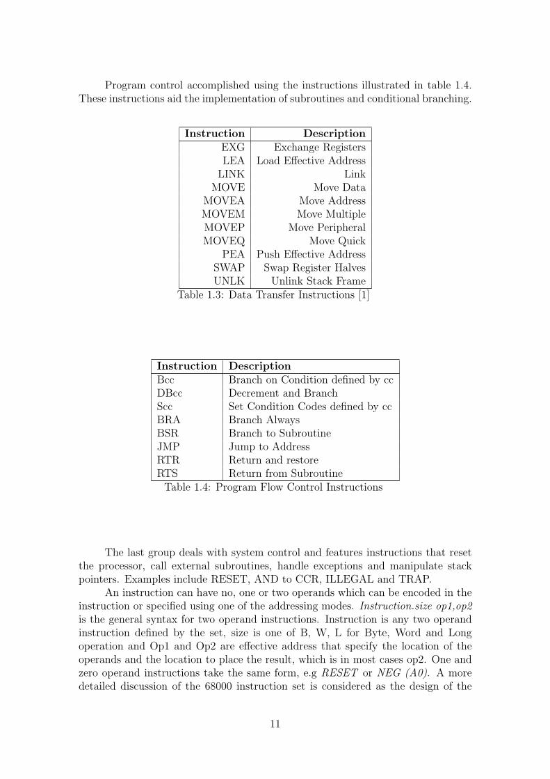
Program control accomplished using the instructions illustrated in table 1.4.These instructions aid the implementation of subroutines and conditional branching.
Instruction DescriptionEXG Exchange RegistersLEA Load Effective Address
LINK LinkMOVE Move Data
MOVEA Move AddressMOVEM Move MultipleMOVEP Move PeripheralMOVEQ Move Quick
PEA Push Effective AddressSWAP Swap Register HalvesUNLK Unlink Stack Frame
Table 1.3: Data Transfer Instructions [1]
Instruction DescriptionBcc Branch on Condition defined by ccDBcc Decrement and BranchScc Set Condition Codes defined by ccBRA Branch AlwaysBSR Branch to SubroutineJMP Jump to AddressRTR Return and restoreRTS Return from Subroutine
Table 1.4: Program Flow Control Instructions
The last group deals with system control and features instructions that resetthe processor, call external subroutines, handle exceptions and manipulate stackpointers. Examples include RESET, AND to CCR, ILLEGAL and TRAP.
An instruction can have no, one or two operands which can be encoded in theinstruction or specified using one of the addressing modes. Instruction.size op1,op2is the general syntax for two operand instructions. Instruction is any two operandinstruction defined by the set, size is one of B, W, L for Byte, Word and Longoperation and Op1 and Op2 are effective address that specify the location of theoperands and the location to place the result, which is in most cases op2. One andzero operand instructions take the same form, e.g RESET or NEG (A0). A moredetailed discussion of the 68000 instruction set is considered as the design of the
11

VHDL CPU instruction decoder is explained in chapter 2. An exact dissection ofthe instruction set can be found in the Motorola 68000 Programmers Manual [10].
12

Chapter 2
Hardware Design
Although implemented in VHDL this project is essentially hardware based. Thischapter explores in detail the 68008 is terms of the hardware implemented to createthe functioning model. Firstly, the functionality of the design is explained followedby how such a design is implemented on the VHDL platform. Initially the designof the data-path including functional unit and register file is considered. Next, BusInterfacing as well as sequencing and control hardware are examined. Where codelistings occur, the source file is quoted and can be found on the accompanying CDin either the 68000-VHDL folder (Xilinx 5.1i) or the X 6800-VHDL folder (Xilinx4.1). Appendix B contains a listing of these files.
2.1 Overview
The hardware design follows loosely the outline of a CISC CPU as detailed in Logicand Computer Design Fundamentals [9, Mano, Kime Pgs: 511 to 542]. However,extensive modifications were necessary to make an MC68008 op-code compatibleCPU and to ensure a Bus Interface was implemented that could support the CPUon an FPGA board. The data-path is modified to perform arithmetic on 8-bit, 16-bitand 32-bit signed or unsigned integers. It was also necessary to add support for thecorrect generation of condition codes as specified by Motorola [11]. The control pathis modified to cater for 16-bit Motorola instruction decoding, the addressing modesoutline earlier and CPU interrupt and exception handling. Control ROM capacity isincreased and the control word expanded to 64 bits. More complex sequencing hasalso been added, to cater for branching within micro-programs and the insertion ofwait stages when interfacing the CPU with peripherals. All internal data transferoccurs through a 32 bit bus. The lower order byte of this bus is valid for a byte(8-bit) operation and the lower order word is valid for word (16-bit) operation. Theremaining bits are either 0 or to be ignored. If a register is being written usinga byte or word operation the lower 8 or 16 bits are the only ones affected by theoperation. An overview of the hardware put in place is found in the schematic onthe following page.
13

2.2 Functional Unit
Figure 2.1: Functional Unit Block Diagram
It is necessary to be able to perform the essential arithmetic and shift oper-ations in this module. Condition code generation must also be considered. TheFunctional Unit consists of two main components, an ALU and a shifter. Two in-puts, A and B feed the ALU operands while The B input feeds the shifter. A sizecontrol input signal is also needed to distinguish between operation sizes. This isparticularly important for the rotate instructions of the shifter and for correct con-dition code generation. In keeping with the Motorola instruction set 00 representsa byte operation, 01 a word operation and 10 a long-word operation. The ALU andshifter are fed simultaneously and each generates a result and appropriate conditioncodes. It is then the function of MUX F and MUX FC to choose the correct condi-tion codes to send to out of the functional unit and to the condition code registers.An operation control inputs selects the desired ALU function. This is detailed intable 2.1. F Select is a 7 bit word that controls the entire operation of the unit. Bit6 is fed to MUX F and MUX FC to distinguish between ALU and shift operations.Bits 5 and 4 respectively carry the extend bit (X) and the carry bit (C) from the
14

system register to the shifter. Bits 3 down to 0 choose ALU operation, and bits 2down to 0 select a shifter operation. A 32-bit result is always generated, however thecorrectness of the generated result is dependant on the size of the operation. Thisis also true for the condition codes generated. The operations supported providefunctionality identical to the Motorola instructions add, subtract, logic and shift op-erations and a basis on which to perform more complex operations such as multiply,divide and add binary coded decimal through the use of micro-programming.
F Select Function00000 Transfer A00001 Increment A00010 A + B00011 A + B + 100100 Negate B00101 Decrement A00110 A B (A + (/B + 1))00111 Transfer A0100x A and B0101x A or B0110x A xor B0111x Negate A1x000 Arithmetic Shift Right1x001 Arithmetic Shift Left1x010 Rotate Right1x011 Rotate Left1x100 Rotate Right with extend (ROXR)1x101 Rotate Left with extend (ROXL)1x110 Logical Shift Right1x111 Logical Shift LeftTable 2.1: Functional Unit Operation Select
This block is also responsible for generation of the negative (N) and zero (Z)condition codes. The Z condition is generated by examining the result and setting aflag if the lower order 8, 16 or 32 bits are all zero. In twos complement arithmetic, themost significant bit determines the sign. If it is 1 then the integer can be interpretedas negative.[8]
2.2.1 The Arithmetic and Logic Unit
The ALU is 32-bits wide and controlled by a 4 bit select input (GSELECT) and a 2bit size input (SZ). Bit 3 of the control signal chooses between logical and arithmeticoperation within the unit. The arithmetic has been implemented using an array offull adders. Following Digital Design [8, Mano pgs 119-120] a HDL description has
15

encapsulated the functionality of a 1 bit adder, correctly generating a sum and carryout given a carry in and inputs X and Y and Z. This full adder was then instantiated32 times using the generate VHDL synthesis function. This function allows multipleinstantiations of the same entity using a loop counter. Other than the first carry in,which is zero, each carry out is fed into the carry in of the more significant adder.
Figure 2.2: ALU Block Diagram
Performing operations
Addition is performed by feeding each individual bit of A and B in to the X and Yinputs of the full adders. The carry will propagate from LSB to MSB and be set inthe most significant carry out. Subtraction is performed by the twos complementmethod. The B operand in first negated, and then incremented to obtain its twoscomplement form and the fed into the Y inputs. The A input is fed as normal intothe X inputs When decrementing A, a twos complement minus 1 is sent into the Yinputs of the full adders. Similarly, for single operand operations such as transfer azero is applied to the Y inputs.
The logic is implemented by feeding each input into the gates in question.These gates are automatically generated by the synthesis tool given correct HDL
16

−− Source : ALU32. vhdBIN <=LongZero when G SELECT=”0000” else −− Transfer A
LongOne when G SELECT=”0001” else −− Increment AB IN when G SELECT=”0010” else −− Add B to AB IN+1 when G SELECT=”0011” else −− A + B + 1Not B IN when G SELECT=”0100” else −− !BMinus1 when G SELECT=”0110” else −− Decrement A(not B IN)+1 when G SELECT=”0101” else −− 2 s Compliment o f BLongZero ;
Figure 2.3: BIN control CSA. BIN Feeds the Y input of the adder array
specification. For example, AOUT <= AIN xor BIN is the VHDL statement that willperform exclusive-or on the inputs AIN and BIN
Condition Codes
The MC68008 uses 5 condition codes to perform branching functions. Overflow, orV, is set when a sign change occurs on an operand. In twos complement arithmetic,which relies on a modulo numbering system, this flag can be generated by an XORon the MSB entered to functional unit input with the MSB of the desired operationresult. A 1 will indicate the sign has changed. The Carry or C flag indicates a carryout of an addition or a borrow out of a subtraction. The C flag is set when themost significant carry of an ALU operation is 1 except for subtraction. The borrowin subtraction is only set if the input operand A is greater than input operand B,otherwise carries generated by twos complement subtraction are ignored and C is0. Extend or X is set to the value of C for arithmetic functions only and is simplyfed out as a replica of the C signal. It remains unassigned for logical operations.The position of the most significant bit of the result in the ALU is dependant onthe size input. When generating Carry and Overflow condition codes for Word andByte operations it is necessary to consider the 16th and the 8-th input and carrybits respectively. Any output more significant than these should be discarded asthey are not guaranteed to be correct.
Implementation and Example
To implement the above two multiplexers decide what enters the X input and whatenters the Y input of the adder array. These MUXs are controlled by G Select. 1for increment, -1 for decrement and (not B) + 1 for subtract are three of the choicesfor the Y input. When only one input is required a Zero is sent through B to theadder array. A bit-vector of 32 bits is used to store the carries, which then can beoperated on using concurrent assignments. A MUX decides which result to send tothe ALU output.
In an example operation we feed 2 into input A and 3 into input B. Subtractionis desired so GSELECT is set to 0110. Twos complement of B is fed from the MUXinto the adder array while A is fed directly. The size of the operation is set to byte
17

(00). Since 2-3 is -1 the output is 11111111 or -1 in byte twos complement form.Carry is set because a borrow has occurred, similarly a sign change has occurred onA and therefore the V flag is set.
2.2.2 The Shifter
The Motorola supports arithmetic shift through ASL and ASR, logical shift throughLSL and LSR, bitwise rotation through ROL and ROR and rotation with the extendbit (X) acting as an expansion to the operand in question through ROXL and ROXR.Arithmetic shifting influences the C and X condition codes. When shifting left theMSB sets carry and extend. A zero is shifted in from the right. Shifting right, theLSB sets the carry and the MSB is shifted in from the left. When rotating the carryis set to be the bit that has been rotated from the MSB to the LSB or LSB to theMSB, the extend bit is not effected unless rotating with extend. In this instance Xis set from C but acts as the LSB or MSB of the operation. Logical shift is exactlythe same as arithmetic shift except 0 is filled in from the left when shifting right.This functionality is encapsulated in the following diagrams.
Figure 2.4: 68000 Shifting. Source : MC68000 Programmers Reference
Implementation and example
The VHDL CPU shifter takes carry in and extend in from the system register.Depending on the size of the operation, combinatorial logic will shift the input leftor right and produce a result. A requirement of shifting is that writing to the systemregister is enabled. This is to ensure condition codes are set correctly and correctoperation of the ROXL instruction. The shifting operations have been implementedin VHDL using combinatorial logic. An example listing is found in figure 2.4. Thiscode piece ensures proper rotation under each operand size. The shifter code causesthe Xilinx synthesis tool to infer a set of multiplexers that generates a barrel-shiftercapable of shifting and left or right once per clock cycle.
18

−− Source : S h i f t e r . vhd−− Rotate Right s e t t i n g carryout to be the ro t a t ed b i tcase SZ i swhen ”00” =>
S OUT(6 downto 0) <= S IN (7 downto 1 ) ;S OUT(7) <= S IN ( 0 ) ;C OUT <= S IN ( 0 ) ;X OUT <= ’0 ’ ;V OUT <= ’0 ’ ;S OUT(31 downto 8) <= ”000000000000000000000000” ;
when ”01” =>S OUT(14 downto 0) <= S IN (15 downto 1 ) ;S OUT(15) <= S IN ( 0 ) ;C OUT <= S IN ( 0 ) ;X OUT <= ’0 ’ ;V OUT <= ’0 ’ ;S out (31 downto 16) <= ”0000000000000000” ;
when ”10” | ”11” =>S OUT(30 downto 0) <= S IN (31 downto 1 ) ;S OUT(31) <= S IN ( 0 ) ;C OUT <= S IN ( 0 ) ;V OUT <= ’0 ’ ;X OUT <= ’0 ’ ;
when others =>S OUT(31 downto 0) <= 32 X ;V OUT <= ’X’ ;C OUT <= ’X’ ;X out <= ’X’ ;
end case ;
Figure 2.5: VHDL Rotate Right using case for combinatorial logic
In an example using the shift-and-add method of multiplication, we are re-quired to shift left and shift right at different stages. Given two byte operands00001000 and 00000011 we are to obtain the result 00011000. Firstly, 00000011 isshifted right one, setting C. This is accomplished by F Select 10110. The carry flagis set and we can branch to the addition part of the algorithm given that code. Nextwe shift 00001000 left one to get the next partial addition. This is accomplishedusing F Select 10111.
2.2.3 Control Registers
The microprocessor uses two registers to control the flow of micro-program anduser-program execution. In order to maintain compatibility with existing 68000code the system register has been designed to match it. As with the 68000 the userbyte contains the condition codes, X,N,Z,V,C. The system byte contains supportfor seven levels of interrupts in IPL2,1 and 0. This holds the current interrupt level
19

and is used in processing external interrupts after every instruction. The S bit, orsupervisor bit, is designed to inform the system whether or not it is executing in useror supervisor mode. In the 68000 programming model certain instructions, such asRESET, may only be executed in supervisor mode. This bit is set when executingsystem level operations such as handling exceptions. The trace bit (T) is set whenthe CPU is operating in trace mode. A trace exception loads in the trace vectorhandler which may contain code to push the system registers to a stack. This isuseful in debugging software as the programmer can see exactly what is containedin all the system registers after every instruction execution.
Figure 2.6: The System Register
The second control register is the Micro-CCR. This register is 4 bits wide andis identical to the SR for bits 0 to 3. The function of the Micro-CCR is to provide aseparate means of tracking conditions generated by micro-instructions. In Microcodethat performs multiple cycle operations it may be necessary to consider conditioncodes generated without affecting the condition codes in the system register. Thisdistinction is illustrated by taking the example above. In a micro-coded shift and addmultiplication we can branch to an addition micro-subroutine if the bit in questionis a 1. This could be done by shifting and using the carry as explained earlier.However, since unsigned multiplication in the 68000 will never produce a carry oroverflow, it is necessary to ensure that the system register carry is not set. Thus,the Micro-CCR provides the codes necessary.
Implementation
The system register is implemented as a 16-bit positive edge triggered register. Loadcontrol of the SR is implemented using combinatorial logic in VHDL and s controlledby the CWORD field MC. Motorola instructions will set condition codes in one of5 ways. Either the SR remains unchanged, C,V,Z,N are changed, C,V,Z,N,X arechanged, Z is changed only, N is changed only or the SR is loaded from the internaldata bus. Also, the trace and supervisor bits must be modifiable and the interruptpriority mask must be changeable. The Micro-CCR has simpler loading logic. TCis the CWORD field that dictates whether or not the CCR is loaded with the codesthat are provided by the functional unit.
20

MC Function0000 Not Loading SR0001 Changing C,V,Z,N0010 Changing C,V,Z,N,X0011 Changing Z only0100 Changing N only0101 Set IPL Mask0110 Set Trace Bit0111 Clear Trace Bit1000 Set supervisor Bit1001 Clear Supervisor Bit1111 Load SRTable 2.2: SR Load Control
2.3 Data Storage and Movement
The processor overview diagram shows how data is moved within the processor.There is an internal 32-bit data-bus that circulates data to the register file, throughthe ALU and to the control-path. MUX D is responsible for choosing betweenexternal data and data from the ALU and placing it on the internal data-bus whereit feeds the rest of the processor. It is controlled by the CWORD field MD andwhen set to 1 reads external data from the Bus Interface.
2.3.1 Register File
The register file contains a bank of 32 registers. Each register is 32-bits wide andis has a load control dependant on the CWORD SZ field. When the size is bytethe lower order 8 bits are loaded and the rest of the register remains unchanged.This is also the case for word writes, except the lower order 16-bits are considered.The register file contains the registers D0-D7, A0-A6 the System Stack Pointer andthe User Stack Pointer (A7). It also contains an internal bank of registers onlyaddressable by micro programs. A Memory Data register and Memory Addressregister are provided to allow the creation of a memory read and memory writemicro-routines. A micro-program can simply place the data that should be writtento memory and the address to where it is to be written into these registers and branchto a micro-routine. The RRW field of the CWORD controls whether a register iswritten or not.
In the Motorola 68000 each instruction will contain at least one effective ad-dress (EA) which will act as a source or destination for operand fetching and writeback. In the same vein as the memory registers EA Data and EA Address areprovided to allow the exploitation of common operand addressing modes within in-structions. The vector address register stores the base address of a to-be-executed
21

Figure 2.7: Register File and Control
exception handler. The remainder of the register file consists of temporary registersT0 to T8 and a Zero provider. The temporary registers are to be used in the storingof intermediate results of micro-operations and micro-programs. The Zero registersimply provides a constant zero for clearing registers.
Register AddressD0-D7 00xxxA0-A7 01xxxSystem Stack Pointer 10000EA Address 10001EA Data 10010Memory Address 10011Memory Data 10100T0 T8 10100 11100Vector Address Register - 11110 Zero Provider 11111
Table 2.3: Internal Register Map
Register Addressing and Selection
Register writing is controlled by an RW signal. A 5 bit destination control is providedto choose a register to write. There are two output ports from the register file tocater for the input of 2 operands into the ALU and to cater for simultaneous selectionof an address register and a data register for placement onto the data and addressbusses.
Since destination and source selection is encoded in a 68000 instruction wordthe register file must be capable of being controlled by the CWORD and by theinstruction currently being executed.
22

The multiplexer FUCTL,FBCTL and SZCTL dictate which entity is control-ling the register file and how. When SZCTL is set to 0 then the CWORD fieldSZ controls the size of an operation. When SZCTL is set to 1 the SZ field is con-trolled by the 68000 instruction word bits 7 and 8, the bits that specify the differentoperation sizes in the 68000 instruction set.
FUCTL feeds the register destination and port A output selection while FBCTLcontrols the B output selection. These multiplexers are instrumental in generatingthe correct register file addresses for destination and selection. When FUCTL andFUBCTL select lines are 000 the CWORD field ASEL,BSEL and DEST controlregister file addressing and all 32 registers are accessible. In a typical 68000 twooperand instruction the instruction bits 3:0 and 11:9 control destination and sourceregisters. When FUBCTL and FUCTL are not 000 these are the bits that controldestination and source selection.
The maximum number of registers addressable with 3 bits is 7. It is thereforenecessary to modify these bits in order to enable access to the Address Registers,located from register 8 to 15. When FUBCTL and FUCTL selections are 001 and 010a 1 is concatenated onto the instruction bits 3:0 and 11:9 to allow the instructionto access a total of 16 registers. It is noted that it is still not possible for theinstruction to access registers reserved for internal operation, this can only be doneby the CWORD. The CWORD must be aware of the addressing mode in order toappend the 1 to any instruction address and access the address registers. Table 2.3gives a list of data registers while Table 2.4 defines FUBCTL and FUCTL operation.
Binary FUCTL FBCTL000 BSEL from CWORD DEST/ASEL from CWORD001 IR[11:9] to B Out IR[11:9] to A Out and Data Reg. Destination010 IR[3:0] to B Out IR[3:0] to A out and Data Reg. Destination011 IR[11:9] to B Out IR[11:9] to A out and Addr. Reg. Destination100 IR[3:0] to B Out IR[3:0] to A out and Addr. Reg. Destination
Table 2.4: Destination and Source Selection in the Reg-ister File
2.3.2 Data Bus and Address Bus Selection
It is necessary in any CPU to provide a means of selecting what is put on the databus and the address bus. This function has been tied into what operands are selectedfor entry into the Functional Unit. MUX A controls the address bus and input A ofthe ALU while MUX B controls the data bus and the B input of the ALU.
MUX A and B assignments
Controlled by the CWORD field MA, this multiplexer has 4 inputs. Firstly, itprovides a means of transferring what is selected on the A port, and the B port of
23

the into the ALU and the address bus. This is done through input 0, A out and 3,B out. This allows any register to be used for addressing, any register to be passedto the ALU or through the ALU to the IR or PC and back into the register file.The second input is the PC. The program counter needs to be placed on the addressbus during instruction fetching and immediate operand fetching. The last input toMUX A is a vector address input. It is necessary to load the PC with a vectoraddress when executing and exception handler routine. MUX A provides a meansby which this address can be transferred from the vector decoder into the registerfile.
Mux B is fed the B output of the register file. The next input is the displace-ment register. This register is used in conjunction with the PC input of MUX Awhen executing instructions that adjust the PC using a 32-bit displacement. Thecurrent IPL mask is also an input to MUX B as it is necessary to compare it withthe requested IPL when processing interrupts. Lastly, the entire system register hasbeen specified as an input. This is to allow for any arithmetic manipulation of theSR that may be deemed necessary and allows the SR to be directly put on the databus when saving the SR during interrupt processing.
MUXes A and B are implemented in code using processes to infer combinatoriallogic.
2.3.3 The IPL control Module
This module is a small entity that stores a pending interrupt request. If multipleinterrupts are requested between interrupt handling then this module will latch thehighest value request. In practical terms this is done using a comparator connectedto the IPL pins and a 3 bit register. This hardware is inferred using the VHDLconstructs detailed below. The signal MUXI is connected to an insanitation of a3-bit positive edge triggered register.
−− Source : Contro l . vhdIPLControl : process (P IPL w , SIG R out )begin
i f P IPL w < SIG R out thenMUX I <= P IPL w ;
elseMUX I <= SIG R out ;
end i f ;end process ;
2.4 The Bus Interface
It is necessary for any CPU to communicate with memory and peripheral devices.As outlined in the introduction, any CPU that is to be put on the FPGA boardmust use a bus interface compatible with the existing bus implementation. The businterface protocols as defined by Motorola for 68008 8-bit operation are compatiblewith the ROM, RAM and ASIC and therefore are sufficient for this purpose. Thisdesign does not strictly follow the timing of the Motorola 68008 bus cycle as defined
24

in the Programmers Manual [10], as it contains certain cycles that are not applicablein this design context (such as empty clock cycles). The atomic Read-Modify-Writecycle has been omitted here as it is only deemed useful in multiprocessor situationswhen using the Test and Set instruction in creating locks. There is scope, however,to add this in at a later time. Similarly bus arbitration cycles have been omitted.However, the strobe generation, insertion of wait states and data bus operation areidentical.
Figure 2.8: Bus Interface Block Diagram
2.4.1 Implementation
To provide abstraction from the CROM, the bus interface has been designed as aseparate entity capable of performing independent bus cycles. Control signals /DS(Data Strobe), /AS (Address Strobe) are generated as necessary. It receives addressdata and operand data from MUXes A and B. The bus interface is connected directlyto the address bus, and through a tri-state buffer to the data bus. A separate tri-state buffer module is used for the data-bus as its abstraction makes it easier tohandle bi-directional communication. The address bus is simply placed in Hi-Zwhen it is not being used and would not benefit from such an abstraction. Whendata is read from the data bus it is passed to MUX D and enters the data andcontrol paths. Due to the fact that data bus is only 8-bits wide the bus interfaceneeds extended functionality to handle reads and writes of words and long words.This essentially entails the BI being capable of multiple read and write cycles in asingle operating mode.
The bus cycles generate signals in a finite sequence and it was decided that aVHDL finite state machine would be the simplest and most readable way of designingsuch an interface. The bus interface is implemented in VHDL using a two-processstate machine. The first process handles clocking. On the positive edge of eachclock cycle it updates a CurrentState register with a NextState register. The secondprocess generates the combinatorial logic to handle state changes. The bus interfaceadvances states depending on assigned inputs and outputs.
25

Figure 2.9: Sample Read Operation State flow (Simplified)
When BIE is high the module is either performing a write cycle, a read cycleor an interrupt acknowledge cycle depending on the input field BI. While theseoperations are being performed the CAR address remains constant and the micro-sequencer only advances the CAR when the bus interface generates a finished signal(PDTACK). The reason for this implementation is to allow for the insertion of waitstages in bus cycles. Since it can not be certain how many wait states will beinserted, simple micro-program NOPs will not suffice and the progression of themicro-program must be blocked until the bus cycle has completed. Any form ofread or write cycle must use the third form of the CWORD, as outline later in thisdocument.
2.4.2 Read and Write Cycles
In order to perform a read cycle BIE is set to enable. It is necessary to choose anoperation using the BI input and provide the bus interface with a pointer to thelocation of the base byte i.e. an address. According to the operation size the businterface will start at state RO and generate the bus signals as indicated in figure2.11. The BI stays in the state R1 until DTACK is pulled low by the peripheraldevice, indicating data is on the bus. The lower byte is then latched in R2 byensuring the tri-state buffer output enable is pulled low in order to read the datadriven by the peripheral device. If the operation is a read-byte operation thenPDTACK is pulled low, causing the CAR to be incremented and the data to readto the CPU registers. In order for PDTACK to effect the CAR in such a way itis necessary for the wait-for-DTACK condition to be set in the CCOND field andthe address of the next micro-instruction to be specified using the 3rd form of the
26

−− Source : BusIn ter face . vhdi f ENABLE= ’0 ’ then−− Wait T i l l We’ re Asked .
ADDR OUT <= ”ZZZZZZZZZZZZZZZZZZZZ” ; −− Not us ing A BusDATA BUS OUT <= ”00000000” ; −− Or data busD OE <= ’0 ’ ; −− d i s a b l e t r i s t a t e outputLatchInt <= ’0 ’ ; −− not l a t c h i n g i n t e r r u p t l e v e lP nBERR <= ’1 ’ ; −− no bus error excep t i onP nHALT w <= ’1 ’ ; −− no h a l tp nDTACK <= ’1 ’ ; −− no dtack to the microsequencerL LByte <= ”00000000” ; −− not l a t c h i n g any by t e sL HByte <= ”00000000” ;H LByte <= ”00000000” ;H HByte <= ”00000000” ;OpSize <= Byte ; −− d e f a u l t o p s i z eRnW <= ’1 ’ ; −− not wr i t i n gnAS <= ’1 ’ ; −− no address on busnDS <= ’1 ’ ; −− no data from usNextState <= i d l e ; −− wai t f o r enab l e
Figure 2.10: Setting outputs for the idle state
CWORD. If the operation is word or long-word then this cycle is repeated 2 or4 times each time incrementing the address pointer and latching the higher orderbytes. PDTACK is not pulled low until the full operation is complete. This way aread-byte or read-longword operation does not have to enable the bus interface 2 or4 times, it is done independently.
In performing a write cycle the CPU sends the address and data to be writteninto the bus interface and selects a write operation and again waits on PDTACK.The strobes are set in as illustrated in figure 2.12 and the write cycle begins. Likethe read cycle the data is written in one-byte increments. When writing to the databus, the tri-state buffer is set to output enable causing the data bus to be drivenout of the high-impedance state.
2.4.3 Interrupt Acknowledge and Bus Error Cycles
68008 supports 3 levels of interrupts, however in keeping with the 68000 7 levelsare supported by the project hardware. Interrupts are processed at the end ofevery instruction, and those generated during an instruction execution are labelledas pending by the IPL control module and processed after the execution. Whenhandling interrupts the bus interface must perform an interrupt acknowledge cycle.When instructed to do so by the control word the Bus Interface module will start aninterrupt acknowledge cycle as illustated with figure 2.13. /AS and /DS are pulledlow, R/W high and the requested interrupt level is fed into the bus interface and onto the address bus lines A0 to A2. If the peripheral wishes to request its own vectornumber /DTACK is pulled low and the vector number is placed on the data bus. It
27

Figure 2.11: Bus Read Cycle
Figure 2.12: Bus Write Cycle
is now up to the micro-program to load and execute the appropriate vector.When opting for auto-vectoring, i.e. when the interrupting device requests
a pre-defined vector address, the peripheral pulls /VPA low instead of /DTACK.The bus interface will generate one of seven vector address and send it to the CPUto be loaded into the Vector Register. The vector handler can now be loaded andexecuted.
The last function performed by the bus interface is Bus Error control. If thebus error flag is pulled low by an external device during a bus cycle then PBERRis pulled low and a bus error exception is generated. During this error handlingFAULTIN is pushed high. If a second bus error occurs during bus fault exceptionprocessing then a double bus fault has occurred and the processor enters the haltstate only to be restarted by reset. This in done by pulling PHALT low.
28

Figure 2.13: Auto-vector peripheral bus cycle
BI Input Function000 Read Byte001 Read Word010 Read Long-Word011 Write Byte100 Write Word101 Write Long-word110 Interrupt Acknowledge111 Reserved for Read-Modify write
Table 2.5: BI Select
29

2.4.4 Bus Interface Hardware
All Bus Interface hardware is inferred automatically with the exception of an 8-bitregister which is a temporary storage register designed to hold the interrupt vector.Latches are used to store intermediate read cycle values, such as the first three bytesof a long-word memory read.
2.5 Sequencing and Control
The most complex section of the CPU hardware design is the control path. Thecontrol path contains logic to generate control signals for the data path and isresponsible for program sequencing and specifying how operands are manipulatedin the design.
There are two common design approaches when considering control unit de-sign. Hardwiring is physically implementing control using a state machine designedwith often complex logic. Hardwired design involves considering the states neces-sary to provide functionality in the data-path and subsequently deducing a statemachine capable of providing this functionality. This approach is the fastest andmost hardware-economical approach to the design. However, this approach is alsoa very inflexible way of creating a design. Specifying hardware control for a CISCinstruction set, which by definition has complexity built in at processor level, isa difficult task. Moreover, once the design has been implemented it is difficult toexpand control without re-wiring the control design in order to add in new states.
Figure 2.14: CROM and Control Address Register
Micro-programming is a less hardware-economical but more flexible approach.An on chip control ROM is used to provide control signals to the data-path. Thecontrol words are provided by an address kept in a Control Rom Address Register.This register is combined with program flow logic to provide Micro-program flowfunctionality. The CROM can be programmed to provide the functionality necessaryan can be easily modified and expanded without modification of the surrounding ar-chitecture [9, Mano, Kime] This is the methodology that has been used in the CPUdesign. It is felt that a micro-programmed design would be easier to understand for
30

anybody wishing to examine the design as it is based on a simple hardware specifi-cation. Also, and more importantly, a CROM design would be reprogrammable andexpandable in future giving the design an increased adaptability. Since the FPGAis based on SRAM look-up tables for interconnection of primitive components thereis no performance advantage in opting for a hardwired approach. A motivation ofthis project is to show how a CISC design may be implemented. The fact thatMicro-coding is used in CISC designs such as the Pentium IV and the 68008 wasanother deciding factor in choosing micro-coding over hardwired control[7]
2.5.1 Control Path Registers
A Motorola instruction consists of a single 16-bit word plus an optional set of exten-sion words that are used to specify addressing mode information and displacementinformation in branching. As a result a 16-bit instruction register is provided and isloaded with the information on the internal data bus when the CWORD field IL ishigh. This register is the outputted to the instruction decoder which is responsiblefor CAR address generation.
The program counter is a 32-bit register, 20 bits of which generates a validmemory address for instruction and immediate operand fetching. It is implementedusing a register and combinatorial logic that generates a load signal depending onthe PL CWORD field. The PL can be incremented in one clock cycle by setting PLto be 01. When PL is 00 the register holds its value. If a 11 is set the PC is loadedwith whatever data is on the internal data-bus. This is necessary to facilitate useof jumping and branch instructions that apply a displacement to the PC.
−− Source : Control . vhdPCControl : p roc e s s (PL w , PCout w , PCInc out , Data In )begincase PL w i s
when ”00” =>MUX P <= PCout w ; −− Hold PC
when ”01” =>MUX P <= PCInc out ; −− Increment PC
when ”10” =>MUX P <= Data In ; −− Load PC
when ”11” =>MUX P <= Data In ; −− Load PC
when othe r s =>MUX P <= ”XXXXXXXXXXXXXXXXXXXXXXXXXXXXXXXX” ;
end case ;end proce s s ;
When processing branching instructions such as BRA or BCC a signed exten-sion word of 32-bits is used to specify a displacement to be added to, or subtractedfrom the PC. In order to facilitate this addition or subtraction in a quick manner,without having to use a temporary register in the file, a displacement register hasbeen provided. Fed into MUX B, it is possible to select the displacement register asa B input to the functional unit, together with the PC into the A input from MUX
31

A and perform the subtraction or addition and subsequent write back to the PC ina single clock cycle.
2.5.2 Micro-sequencing
A micro-sequencer is the lynchpin of any micro-programmed architecture. It isresponsible for the generation of the next CAR address thus defining the next set ofcontrol signals to be applied to the data-path.
Figure 2.15: Microsequencer Block Diagram
The CROM has been designed as 4096 words deep, meaning a 12-bit address isrequired. This gives ample space for micro-coding the 68008 instruction set providedthe micro-programs are written in a modular fashion and take advantage of common
32

operations between code. For example, the micro-code for a memory write willbe the same for every instruction write-back, therefore it makes sense to re-usecommonly invoked micro-addresses. A 12-bit Control Address Register (CAR) holdsthe address of the currently executing microinstruction. The loading of the CARis controlled by the CAR increment register and multiplexers MEX, MCA, MNA,MCD and B/SEL. At every stage the CAR increment register contains the valueCAR + 1. The CAR is loaded on the positive edge of the clock, so it is necessary tomake the CAR increment register negative edge triggered, to allow for propagationthrough the register and back to the CAR in a single clock cycle when a CARincrement is desired. The CWORD field MCA controls the multiplexer that loadsthe CAR. Table 2.6 details the effect of this field on the CAR.
MCA Function000 Increment CAR001 Load From MicroStack010 Load From Single Branch Register011 Load CAR from Instruction Decoder100 Load CAR using Motorola Conditions
Table 2.6: MCA Selection
The Micro-Stack and SBR
To aid the use of micro-routines a Micro-Stack architecture has been implemented.There are 5 registers provided in which are placed return addresses when imple-menting branching within the micro-routine. Registers BR0 to BR3 are part of theMicro-Stack and provide 4 levels of branching within micro-routines. The Micro-sequencer contains a two bit counter, the Micro-Stack pointer, which controls theloading and selection of these four registers. When calling a micro-subroutine theMSPI field must be set to 01 in order to increment the stack pointer. In the nextclock cycle BRLoadControl must be set to 01. This causes the next CAR address+ 1 to be placed into a specified load register. It is now possible to load the CARwith a micro-routine address specified by next address. During the execution ofthe sub-routine, the micro-stack can be used again for the same purpose. Whenreturning from a subroutine it is necessary for the micro-routine to load the CARwith a return address. This is done by setting BRControl to 11 and MCA to 01.The address popped off the stack is equal to the calling address + 1. The callingmicro-program must now decrement the stack pointer by setting MSPI to 11 beforeit can continue processing. This micro-architecture mimicks how a stack may be im-plemented in software. A pointer holds the location of the next point on a stack. Amicro-stack operation i.e. push or pop, is an atomic micro-operation but in practiceat this low level takes two clock cycles, once to ensure the pointer is at the correctlocation, one to perform a push.
This implementation provides a very powerful means of branching within mi-
33

crocode. For example, when an instruction is decoded the CAR is loaded with anaddress for the micro-program that must be executed. This micro-program will mostof the time need to fetch operands on which to perform operations. If an effectiveaddress is designated as the source, one of the addressing modes must be used tofetch this operand. With the micro-stack implementation it is possible for an in-struction micro-program to branch to an addressing mode micro-routine, e.g. fetchaddress register indirect, which will place the result in the EA Data register. Whenfinished fetching operands the instruction and continue execution and write-back.
The Single Branch Register, or SBR is a branching register that is not part ofthe stack. Its intended use is for memory access. Since a memory access will nevercontain a branch, it is spared the need to use up 3 cycles manipulating the stackpointer and micro-stack. Instead it simply loads and unloads the Single Branch DataRegister as necessary. This also means that even micro-routines with addresses atthe top of the stack may use the Bus Interface for memory reading and writing. SLloads the SBR and when MCA is 10 the CAR is loaded with the value in the SBR.
Figure 2.16: Micro-Branching Flow
Conditional Branching
MNA, MCD and the Next-Address input allow conditional loading of the CAR. Itis necessary to support a variety of conditional load conditions that may arise fromboth the Micro-CCR and the User Byte of the SR. When the MCA is set to 100
34

the inputs CCOND and ACC decide what to load the register with next. Table 2.7details the operational values of the 5 bit CWORD field CCOND. When performinga branch in a micro-routine it is necessary to provide the micro-sequencer with anaddress to load if the branch is taken. If the condition chosen is high at the timespecified, and the allow condition (ACC) field is 1 then the CAR is loaded with abranch address from the NA field. If the condition is a zero at the time specifiedthen the CAR is simply incremented.
Value Description00000 Branch Carry Set (Micro CCR)00001 Branch Overflow Set (Micro CCR)00010 Branch Zero Set (Micro CCR)00011 Branch Negative (Micro CCR)00100 Branch Carry Clear (Micro CCR)00101 Branch Overflow Clear (Micro CCR)00110 Branch Positive (Micro CCR)00111 BCS Motorola (C)01000 BVS Motorola (V)01001 BEQ Motorola (Z)01010 BMI Motorola (N)01011 BCC Motorola (/C)01100 BVC Motorola (/V)01101 BNE Motorola (/Z)01110 BPL Motorola (/N)10011 Wait for Bus Interface Finished Set10110 BHI Motorola (/C*/Z) Branch Higher10111 BLS Motorola (C + Z ) Branch Low or Same11000 BGE Motorola (N*V + /N*/V) Branch greater than or equal11001 BLT Motorola (N*/V + /N*V) Branch Less than11010 BGT Motorola (N*V*/Z + /N*/V*/Z) Branch Greater Than11011 BLE Motorola (Z + N*/V + /N*V ) Branch Lest than or equal11100 Force Load of NA
Table 2.7: CCOND Possible Branching Conditions andCCR Codes
In the shift-and-add multiplication example detailed previously it was sug-gested that the multiplicand be shifted left one place setting the carry to be a 1if the LSB is a 1. It was suggested that a branch be taken if the carry is notset to avoid adding a partial product un-necessarily. The following describes howthis is implemented using the micro-sequencer and the Micro-CCR Carry and Zeroconditions.
ADDRESS CCOND MCA NA DESCRIPTION
35

$4 0000 000 N/A −− S h i f t the mu l t i p l i e r l e f t$5 1010 100 $7 −− Branch i f Carry Clear to $7$6 0000 000 N/A −− Otherwise add p a r t i a l product$7 0000 000 N/A −− S h i f t the sum of product s l e f t$8 0000 000 N/A −− Sub t rac t 1 from a loop counter$9 1010 100 $4 −− Branch Zero Clear to the s t a r t$10 1010 100 $11 −− Write Back Operation us ing BI$11 0101 100 $24 −− Jump to f e t c h next i n s t r u c t i o n
There is one exception to this general application. When CCOND is set towait for DTACK, the current CAR address is reloaded, rather than CAR + 1. Thisis designed to allow the bus interface to complete its cycle fully. In this instancethe next CAR address must be specified by using the Next-Address input. Whenperforming a bus cycle that requires the insertion of wait stages it is necessary tohave the address of the next instruction to be executed in the next-address field.
Handling Bus Error and Halt Exceptions
The final multiplexer feeding the CAR is concerned with the loading of exceptionhandlers. There are three possible exception handler addresses that may be loadedinto the CAR. If a Bus Error occurs, the bus interface will generate the exceptionsignal. This causes the CAR to be loaded with the bus error exception handler. Thishandler can simply load the vector register with the bus error vector number. Thisloading in necessary since if the BI is active, the car NA will remain stationary. Theonly other exception that is supported using this method of loading is the HALThandler. A programmer may wish to push information to the stack before enteringthe halt mode.
An Internal Exception field IE has been placed in the CWORD for futureuse. The use of this function is to enable the generation of exceptions within micro-programs. The Motorola generates exceptions upon the results of certain operations.For example a divide by zero will cause and exception handler to be run. Similarlyif the TRAP instruction is called a handling program must be loaded. The IE fieldallows these software exception handlers to exploit commonality. Each exceptionmay place its exception handler address on the stack and push high the IE field.This IE field may load an exception handler that pulls this vector address off thesystem stack and processes as necessary.
2.5.3 Instruction Decoding
An MC68000 Instruction consists of at least one 16-bit word. In order to facilitatevarious addressing modes there may be up to 11 extension words. These words maycontain information such as immediate operands, source and destination effectiveaddress information or branching displacement information.
An instruction may specify zero, one or two effective addresses within an in-struction word. An effective address is a 6-bit substring of the full instruction word.It provides information as to the source and/or destination of operands as well asthe addressing mode that is used in order to fetch those operands. The majority of
36

instructions will use a single effective address which may specify the destination ofthe operation or the source operand.
Figure 2.17: Effective Address Field
The mode field of the effective address gives information as to the addressingmode of the effective address. The register field will either specify a register in whichthe operands or information about the operands is contained. It may also containinformation relating to addressing mode. Table 2.8 shows how the effective addressmay be decoded.
MODE REGISTER DESCRIPTION000 xxx Data Register Direct001 xxx Address Register Direct010 xxx Address Register Indirect011 xxx Address Register Indirect with Postincrement100 xxx Address Register Indirect with Pre Decrement101 xxx Address Register Indirect with Displacement110 xxx Address Register Indirect with Index111 000 Absolute Short111 001 Absolute Long111 010 PC indirect with Displacement111 011 PC indirect with Index111 100 Immediate
Table 2.8: Decoding an EA
When using the immediate addressing mode the immediate data is specified inan extension word. When using the displacement or index addressing modes the ex-tension words will contain the displacement that is needed to perform the necessaryoperation. Figure 2.18 shows how a MOVE instruction is encoded and stored inmemory. The MOVE is the only instruction that may have two effective addresses.Other instructions must store the results in destinations specified elsewhere in theinstruction.
Figure 2.18: MOVE.B #5,(A0) Instruction
37

Bits 15 down to 6 of a 68000 instruction are used for decoding the instructiontype. Bits 15 down to 12 can be used to form a loose grouping of instructions. Forexample, 0000 in bits 15 down to 12 will indicate that the instruction is either an im-mediate instruction, such as ANDI, or a bit manipulation instruction such as BTST.As detailed in figure 2.19 it is possible to break up the remainder of the instructionin to well defined pieces in order to work out what instruction is being executed. Infig 2.19 bit 7 differentiates between Bit Manipulation and immediate instructions.Bits 11-8 specify the sub-group of these instructions and the remainder specifiesoperand size and effective address. For example when 8 is 0 and OPC is 000 we aredealing with an ORI instruction, a member of the immediate instruction functionalgroup. Not all instruction formations are as regular but a similar breakdown can beapplied to the majority of instructions.
The form 1111 of the leading 4 bits is reserved for interrupt processing, but theremainder will specify one of several instruction groupings such as the Immediate/Bit-manipulation grouping. The accompanying CD-ROM contains an excel spread sheetwhich is a guide to the instruction groupings proposed and used in this project.
Figure 2.19: Instruction encoding for group 0000
If the instruction is a two operand instruction, bits 11 down to 9 will alwaysspecify a register number. How this number is interpreted depends on the instruc-tion. For example, ADD (ea),Dn will interpret this register as the source for thesecond operand in the addition, and also the destination for result write-back. Inthis instance the EA will specify the source operand. Size is encoded in one of twoways. Bits 7 and 6 (SZ) contain size information for applicable instructions exceptin the case of MOVE where bits 13 and 12 (SZ2) dictate operation size.
The Instruction Decoder
A mapping ROM with an address manipulated by combinatorial logic is used toprovide the CAR with CROM addresses depending on the operation desired. Theselect input ISEL controls the operation of the decoder and allows decoding of dif-ferent parts of the instruction such as the EA and the main op-code. The instructiondecoder will provided CAR addresses in one of four ways. Firstly, it will provide theCAR address for the execution of one particular instruction. In this instance theCWORD field ISEL is set to 000. The mapping ROM address is constructed fromthe instruction word bits 15 down to 6 concatenated with a 0. All mapping ROMaddresses that start with 0 are responsible for the decoding of the function of aninstruction. For example mapping ROM location 00000001000 contains the CARaddress that will run the micro-program dealing with the ANDI instruction.
When the ISEL input is 001 the instruction decoder is performing a decodeon an EA and is using this EA to fetch operands. 100—SZ—EA is fed into themapping ROM giving the location of the required address. For example, location
38

Figure 2.20: Instruction Decoder and mapping ROM
100—00—010000 will contain the CAR address for a byte-operand fetch using theaddress register indirect addressing mode.
ISEL 010 is identical to the above operation except it performs decoding on bits11 down to 6 for a move instruction. Locations for such CAR addresses are producedby the word 101&SZ2&EA. 011 and 100 operate in a similar fashion except they areresponsible for supplying the CAR with addresses necessary for operand write backwhen the effective address is a destination.
The locations of thee words in mapping ROM and CROM memory are donein Xilinx through the use of constants. For example, the write micro-routine.
−− Source : CROM4096x64 . vhd−− Dec lara t ionconstant Read Byte Wait : s t d l o g i c v e c t o r (63 downto 0) := . . .constant Read Byte Latch : s t d l o g i c v e c t o r (63 downto 0) := . . .constant Read Byte Return : s t d l o g i c v e c t o r (63 downto 0) := . . .−− Mappingwhen ”111111110011” => output <= Read Byte Wait ;when ”111111110100” => output <= Read Byte Latch ;when ”111111110101” => output <= Read Byte Return ;
2.5.4 The Control Word
The CROM is a 4096 deep ROM that produces control words of 64-bits in length.It is possible to restrict the size of the word to 64-bits by defining the word threeforms shown in figure 2.21. The first form of the word is intended for operation ofthe system that does not involve jumping or branching. In this instance bit AA is0 and bits 22 down to 17 influences loading of control path registers.
In order to use the functional unit and the system control registers it is neces-sary to use this form of the CWORD. The second form of the word sees the inclusionof an 8 bit vector number. This form is only used for the decoding of an 8-bit vector
39

Figure 2.21: CWORD Formats
number which is subsequently loaded into the Vector Address register for executionof an exception vector. The third form of the control word sees the inclusion of theCCOND field and the next address field. The CCOND field selects the conditionfor branching and the next address specifier will give the next address if a branchis taken. The functional unit field have been used in this instance since when func-tional operation is used in a micro-program it will always occur before the branchand never in the same clock cycle.
Table 2.9 gives a breakdown of the function each field performs. Appendix Agives a full list of the valid values of each field.
40

FIELD BIT NUMBERS FUNCTIONBSL 2:0 Bus Interface Operation SelectBE 3 Bus Interface EnableFI 4 Processing a Bus FaultFBC 7:5 R/File Port Control SelectFUC 10:8 R/File A Port/Destination Control SelectMCA 13:11 MicroSequencer CAR Address Source SelectMP 15:14 MicroStack Pointer ControlACC 16 Allow Condition Codes to effect CARPL 18:17 Program Counter Load ControlDP 19 Displacement Register Load EnableIL 20 Instruction Register Load EnableCCOND 21:17 Branch Condition SelectSL 22 Single Branching Register Load EnableD 61—24:23 Instruction Decoder Function SelectASEL 29:25 Register File Port A SelectBSEL 34:30 Register File Port B SelectDEST 39:35 Register File Destination selectSZ 41:40 Operation Size SelectSS 42 CWORD/Instruction for SizeMC 46:43 System Register Load ControlFS 51:47 Functional Unit Operation SelectVector No 51:44 8-bit Vector numberNext Address 61:59—51:43 Next Address LoaderMA 53:52 Mux A SelectMB 5:54 Mux B SelectMD 56 Mux D SelectTC 57 Micro-CCR Load EnableRW 58 Register File Read WriteBR 60:59 MicroStack Load/Unload ControlIE 62 Generate Internal ExceptionAA 63 Allow Next Address field
Table 2.9: CWORD Field Function
41

Chapter 3
Micro-programming the design
Once all needed hardware was in place and individually tested was necessary to con-sider micro-coding. This chapter explores the micro-programs necessary to controlthe system by specifying how micro-program algorithms may be implemented usingthe hardware in place.
3.1 Control Word Generation
Micro-coding a 64-bit word is a tedious, error prone task when done by hand. Tocombat this tedium and to decrease the chance of errors during CPU operation asimple Visual Basic application has been developed to automatically generate controlwords given specified inputs. The generator has been programmed in Visual basicbecause of its ability to quickly generate forms and automatic generation of essentialMFC code.
The application contains a series of drop-down boxes detailing possible valuesfor each control word field. The user specifies the desired value for each field andthe application constructs the appropriate CWORD, which then can be copied tothe Xilinx application or ROM bit file.
Operation is intuitive for programming a CWORD of the standard form. How-ever, when programming branching and vector addresses there are some necessaryomissions. In keeping with the CWORD format, the fields Micro-Stack Control(BR),Function Select, SR Load Control, SQ, IR Load, Displ Load and PC load must allremain blank. Allow CC must be set to conditions for a conditional branch. Thisfield can be ignored when supplying a vector number to the vector address regis-ter. Next address locations and vector numbers can be inputted into the providedtext-boxes. Although not yet implemented, it is intend that a drop-down list ofcommonly used next CAR addresses, such as instruction fetch and memory accesseswill be able to provide next address values. Similarly, it is intended the complete68008 memory addressing list be added.
42

Figure 3.1: Generating a CWORD to Add D0 to D1
3.2 System Control Programming
In order for the system to function correctly a number of system control micro-programs must be implemented. These micro-programs provide a skeleton set ofmicro-routines on which actual micro-programs can be constructed.
3.2.1 Memory Access
Since the first instruction of any program will be held in memory the first micro-program necessary is one that will control memory access. All memory accesses inthe system are implemented using the memory access micro-routines. It is intendedthat these routines be called from micro-programmes that require memory access,such as memory operand fetch or instruction fetch. There are routines for memorywrite and read of each size of operand.
12-bit Hex Address RoutineFF3 Read ByteFF0 Read WordFC0 Read Long-WordFC8 Write ByteFCA Write WordFCC Write Long-Word
Table 3.1: Memory Access CROM Locations
43

Each of the memory reads takes three micro-instructions while the memorywrites take two. The number of clock cycles taken depends on the size of the buscycle and the number of wait stages inserted by the bus interface.
The reserved memory address register provides the Bus Interface with a lo-cation from which to read a memory address. If the operation is a write then theresult is placed in the reserved memory data register.
The first micro-instruction sets the bus interface to enable and waits for thePDTACK signal. For example when reading a byte, the BIE field is set to 1 and theBI field is set to 000 for a read. The third CWORD form is used and the branchcondition is PDTACK. The next address is fed from the CWORD and is set to FF4in order to load the next micro-instruction when the data has been received fromthe peripheral device. MCA is set to next address in this instance. For memoryread an address must be provided from the register file. Similarly source data mustbe provided for a write. MUX A must be set to transfer an address and MUX Bmust transfer the necessary data to the bus interface
Upon assertion of PDTACK the second micro-instruction is loaded. This in-struction is responsible for the reading of data from the bus interface. The memorydata register must be selected as the destination register and the register file mustbe set to CWORD control (FUCTL = 000, FUBTL = 000). Register write mustalso be enabled. The size field must be set to 00 for byte and the SS field mustindicate that size selection is under CWORD control. The last micro-instruction iscommon to all memory access subroutines and is a return from routine instruction.This instruction simply loads the CAR with the value located in the single branchingregister, thus returning to the calling micro-program.
3.2.2 RESET Handler
When the 68008 is powered on for the first time, or is reset it must initialise the PCand the system stack pointer. The first long-word of memory, location 0, will containthe initial system stack pointer. The second long-word will contain the initial PC.
In the 68008 VHDL model the PC is reset to 0 by the nRESET signal. Ittherefore makes sense to use the PC as a pointer to retrieve the initial stack pointerand the initial PC. Branching to the memory micro-routine is not used in thisinstance as we intend to us the PC as a memory address pointer. Ten instructionsare required the first of which is located at CROM location 0.
We must initialise the bus interface and wait for PDTACK as if performing amemory read. On the next micro-instruction we are required to load the SSP. This isdone by setting the register read field to write and selecting system stack pointer asthe destination. The same must be done for user stack pointer, as, although in theorythe same register, they are represented in hardware by two different registers. ThePC is then incremented 4 times by setting PL to load for 4 consecutive instructions.
The next bus interface cycle required field is a read-long word for the PC. Thisaccomplished using the initial PC as a source like before. On the next instructionit is necessary to set the PL field to Load and MUX D to External in order for itto latch data fed from the bus interface. The final instruction simply jumps to thelocation of the Instruction Fetch micro-routine.
44

3.2.3 Fetch-Decode-Execute Sequence
All processors need to perform this cycle in order to fetch and execute instructions.Located at CROM location 0x00F the instruction fetch micro-programme operatesin exactly the same way as the initial PC fetch routine except a 16-bit word isfetched and the IL field must be set to load instead of PL.
Once the instruction register has been loaded the PC is incremented twice topoint to the potential location of the next instruction in memory. It is now desirableto jump to instruction decode. In order to do this the third CWORD form must beused and the location of the ID routine, or 0x808, must be fed to the next-addressmicrosequencer port. MCA is set to Load Next Address, ACC to Conditions andthe condition field CCOND must be set to NALOAD. The CAR is now loaded withthe ID routine.
Figure 3.2: The Fetch-Decode-Execute Cycle
The ID routine itself is a simple jump. MCA is set to Instruction Decoder andthe ISEL field is set to Opcode. The instruction decoder will decode the instructionand provide a location for its execution which is then fed into the CAR.
The processor is now in the execution phase. Due to the varied nature ofthe location of operands in the 68008 instruction set, and to the fact that notall instructions may access all addressing modes, each execution micro-program isresponsible for the fetching and write back of all operands as well as instructionexecution.
Interrupts
Once write back has been completed it is necessary to check for interrupts. Anyinterrupt requested during execution is processed by the IPL control module. Ifmultiple interrupts are requested during an instruction, the highest level one isconsidered only.
The CWORD field SQ allows the register file to be loaded with the valueemanating from the IPL control. Temporary register T0 is loaded with this value.On the next clock cycle this register becomes an A input to the ALU by settingASEL to T0 and MUX A to 00. MUX B IPL select will provide the ALU inputwith the current interrupt level. A subtraction is performed and the MicroCCR isset using the appropriate signals for TC and FS.
45

If the result of the operation is negative the current interrupt level is higherand the interrupt is rejected. This is accomplished by setting MCA to Next Addressand the condition in question set to branch not negative from MicroCCR. If N is setit will cause a jump over the instruction that deals with processor interrupts andback to instruction fetch for the next instruction.
If this jump is not taken then a jump to interrupt processing will take place.The procedure is as follows
• Save the status register to the system stack.
• Save the PC to the system stack.
• Perform an interrupt acknowledge cycle using the Bus Interface.
• Obtain vector and load to PC.
• Return from interrupt (RTI) is called and original PC and Stack Pointer arerestored.
3.3 The MOVE instruction
This section explains in detail how the MOVE instruction is implemented and definesthe process by which all micro-programs should be written. It includes details ofthe addressing mode fetch and write-back micro-routines implemented to date. TheMOVE micro-program is located at 0xC20 in the CROM and is 7 words deep.
3.3.1 Decoding
In order to provide the CAR with the correct address for the MOVE instructionit is necessary to place that address in the decoder mapping ROM. Since we aredecoding a main instruction, the MSB of the mapping ROM address is 0. TheMotorola programmers manual specifies the first two bits of an instruction to be 00.We firstly want to deal with word operands, therefore the next two bits are 11. TheMOVE instruction form is shown again in figure 3.3. It is necessary to place 0xC20,or the MOVE micro-program address, at locations 00011xxxxxx of the mappingROM in order for correct decoding to be performed for all addressing modes for thedestination.
Figure 3.3: MOVE Instruction Form
46

3.3.2 Fetch using Addressing Modes
Once the MOVE instruction micro-program address has been decoded the micro-sequencer will start executing the MOVE micro-program itself. As previously ex-plained, it is necessary to fetch the source operand for the operation. As a result thefirst 2 instructions of the MOVE routine simply increment the MicroStack pointerby setting MSPI to 01 and push a return address on the MicroStack by setting theBRLoad field to 01. It is necessary to decode the source effective address for aMOVE so 101 is fed into DSEL field.
Five forms of operand fetch addressing modes have been implemented in micro-coding and hardware support exists for the remainder. These are Data RegisterDirect (CROM location 0x03F), Address Register Direct (0x041), Address RegisterIndirect (0x043) and Immediate (0xE00).
All addressing mode micro-routines will use at least one of the registers re-served for effective addresses and the memory read and write registers. Taking theImmediate addressing mode as an example it is possible to show how a typical fetchmicro-routine will operate.
Immediate operand fetch will move the data encoded in an instruction exten-sion word to the Effective Address Data register. An immediate operand of length16-bits is located in memory at the address immediately following the core instruc-tion word. The instruction op-code for an immediate fetch is encoded in the lowereffective address. Motorola uses 111 for mode and 100 for the register field to in-dicate an immediate data addressing mode. Instruction decoder mode Fetch forMove is used and therefore the micro-routine address must be located at address10111111001. When source effective address decoding has taken place the Imme-diate micro-routine is in execution. A Bus read cycle for a word operation mustbe performed. As before the DTACK condition is fed into the CCOND field, AAis set to 1, bit 16 is set to 1 and the next address (the location of the next micro-instruction) is fed into the NA field. After the bus cycle the register Effective Data iswritten. The PC must now be incremented twice following which the micro-routinewill return to the MOVE instruction by setting BRLoad to 11 and MCA to 001.
MOVE3 is concerned with setting the correct condition codes. It is necessaryto circulate the Effective data Register around the ALU using the Transfer functionin order to set the correct condition all condition codes except eXtend are affected.MUX A simply reads the register circulates as the A input of ALU and MC is setto allow all codes except X to be set.
3.3.3 Write Back
Most instructions give the option of using the effective address as a destinationinstead of a source. The MOVE instruction allows both to be an EA. In either casea write-back micro-routine must be called.
Write back routines have been implemented for the MOVE instruction only.These include Data Register Direct (CROM location 0xE05), Address Register Di-rect (0xE07), Address Register Indirect (0xE09), Address Register Indirect withPost Increment (0xE11) and Address Register Direct with Pre-Decrement (0xE18).
Decoding is performed by setting ISEL to 100. The address for the write-back
47
micro-routine must be put in its correct mapping ROM place for EA write back ona MOVE instruction. ”111” & SZ2 & EA2 is the address string that will determinethis. SZ2 is instruction bits 13 down to 12. EA2 is the destination effective addressin a move instruction and consists of bits 11 down to 6. For example, data registerdirect write back for a MOVE.W instruction must be located at mapping ROMaddresses 11111000xxx.
The write back routine will expect to find data to be written back in theEffective data register. If an address is necessary then it is expected to be located inthe Effective Address register. All memory-modifiable addressing modes will movethis data to the Memory Data and Memory Address register before branching to aBus-write cycle.
3.4 The MULU instruction
The MULU instruction performs a multiply on two, at maximum, 16-bit unsignednumbers and stores the result. This instructions micro-coded implementation isexplored in order to give an example of how one might implement a complex in-struction that requires multiple-clock cycles to execute. Operand fetch and writeback for MULU are performed in a similar way to that of the MOVE instructionand have not been considered here. The MULU instruction has been located atCROM 0xA0F and requires thirteen instructions six of which are repeated sixteentimes for a total of 97 clock cycles. It is noted here that a hardware multipliercan complete such a task in less clock cycles however micro-coding instructions thisway is consistent with the CISC design approach and is good way of testing correctfunction of the control and sequencing logic.
3.4.1 The Shift-and-Add Algorithm
The Shift-and-Add algorithm of binary multiplication is used in this example. Thismethod adds the multiplicand Y to itself X times, where X denotes the multiplier.[15,Zargham CH:2 S:2.5.2].
The first task of shift-and-add multiplication is to set up the temporary regis-ters necessary to perform the operation. The multiplicand is placed in T0 and themultiplier in T1. T3 is used as an accumulator register and stores the results ofpartial products at every stage of the multiply. A constant value of 16 is placed inregister T8. This will count the number of iterations necessary for the multiplication.
MUL4 shifts the multiplier right and allows the MicroCCR condition codesto be set. This is done by choosing logical shift right for the FS field and settingTC to 1. The result is stored back in register T1. MUL5 uses the branching formof the CWORD, sets Branch Carry Clear to be the condition in the CCOND field,bit-16 to be a 1, AA to be 1 and the location of MUL7 to be the next address. Ifthe MicroCCR has shifted a 1 into the carry then MUL6 will be executed. MUL6simply adds T0 to T3. If carry is clear then MUL6 is not executed and MUL7 isthe next address. MUL7 shifts T0 left one. MUL8 subtracts 1 from T8 and sets theMicroCCR again. MUL9 is a branching Micro-Instruction that returns to MUL4 if
48

T8 is not zero, otherwise proceeds to MUL10 which is responsible for operand writeback.
−− Source : CROM4096x64 . vhdconstant MULU S . . . −− Clear accumulator r e g i s t e rconstant MULU 0 . . . −− Move 8 to Temp 8constant MULU 1 . . . −− Move source to Temp 0constant MULU 2 . . . −− Move d e s t i n a t i o n to Temp 1constant MULU 3 . . . −− Move Temp 0 to Temp 2constant MULU 4 . . . −− Log i ca l S h i f t r i g h t T1 s e t t i n g MicroCCRconstant MULU 5 . . . −− Branch Carry Clear to MULU 7constant MULU 6 . . . −− Add Temp 0 to Temp 3 s t o r e in temp 3constant MULU 7 . . . −− Log i ca l S h i f t Le f t Temp 0constant MULU 8 . . . −− Sub t rac t 1 from Temp 8 s e t c . codesconstant MULU 9 . . . −− Branch i f Temp 8 not Equal to 0 to MULU 4constant MULU 10 . . −− wr i t e back to de s t . S e t t i n g codes
3.4.2 Other Instructions
Other instructions have been implemented in exactly the same way using the Micro-Word generator and using the following technique.
• Assign a CROM Location.
• Ensure correct decoding of the instruction suggested groupings.
• Use the Micro-Word Generator to generate micro-instructions.
Other implemented instructions to date are JMP, ADD, SUB (for Direct ad-dressing) and BMI (branch on minus).
49

Chapter 4
Testing and Conclusions
This chapter details what has actually been accomplished during the project by ex-ploring some test results and stepping through a demonstration of a 68000 assemblyprogram. Suggestions for further avenues of work on this project are also explored.
4.1 Design Testing and Development Progress
All design testing has been performed using ModelSim. A simulation on this plat-form allows the designer to isolate any wire, register or signal contained within thedesign. This very powerful tool was a vital component in debugging the operationof the VHDL CPU and
Each individual module has been tested using test-benches designed to verifythe functionality on all possible inputs, or when that is not feasible, a set of in-puts that practically verifies module operation. Top-level testing was accomplishedthrough strategic implementation of micro-code. As micro-coding the system for thefull instruction set is a time consuming task, a focus has been placed on using se-lected micro-coded applications to test the fully inter-connected system. As a resultthe micro-code in place to-date will verify the inter-operation of all the modules. Forexample, MULU will test branching and sequencing, MOVE the addressing modecapability and the bus interface and RESET the handling of exceptions.
Most of the problems encountered throughout this project were results of im-plementation mistakes. For example, an early implementation of the control pathattempted to specify the unit in such a way that the Xilinx synthesis tool would au-tomatically infer control logic. This proved to be an error-prone and unreliable wayof implementing control as the design was unnecessarily complex and hard to follow.It was at this early stage that the decision to keep to an RTL level of abstractionwas made.
Other problems stemmed from common mistakes such as incorrect behaviouralimplementation results. In an example the ALU was not generating proper resultsand condition codes for the subtract function. The ModelSim platform enabledexamination of each part of the design to isolate this problem to a programmingmistake.
As previously outlined, the project has been developed to a stage where allnecessary hardware needed for a VHDL op-code compatible CPU has been put in
50

place. All modules have been tested and confirmed operational under behaviouraland post-synthesis simulation. In addition a substantial subset of the micro-codingnecessary for full instruction set decoding has been completed and tested undersimulation.
4.1.1 Synthesis
A successful synthesis has been performed on the design using the Xilinx synthesistool targeting the Virtex-II VC1000-256fg FPGA. A synopsis of the synthesis reportcan be found below.
The design uses 3,131 slices of Virtex-II resources, or approximately 61% ofthe slice resources available to the FPGA. In comparison, the modified LEON coreutilises approximately 62
Design Summary:Number of errors: 0Number of warnings: 4
Number of Slices: 3,131 of 5,120 (61%)Number of Slices containingunrelated logic: 0 of 3,131 (0%)
Total Number Slice Registers: 1,267 of 10 ,240 (12%)Number used as Flip Flops: 1,233
Number used as Latches: 34Total Number 4 input LUTs: 5,547 of 10 ,240 (54%)
Number used as LUTs: 5,495Number used as a route -thru: 52Number of bonded IOBs: 105 of 172 (61%)Number of Tbufs: 20 of 2,560 (1%)Number of GCLKs: 1 of 16 (6%)
Total equivalent gate count for design: 47 ,675Additional JTAG gate count for IOBs: 5,040Mapping completed.
The gate count for the designs differ dramatically however, with the LEONcore using almost three times the number of gates used by the 68008 design. Thisis most probably due to the more complex pipelined logic of the LEON core, whichhas hardware such as a floating point unit which are not found in the 68008 model.
Implementation timings are shown below. The maximum clock period attain-able by the current design is 11.718Mhz. The FPGA project board has an 8Mhzclock port, therefore the design is more than capable of handing this clock speed.It is noted that it may be possible to increase this clock speed by examining thedesign for critical paths and re-organising the design to suit, however, as previouslyoutlined, the nature of the project requires the 68008 model to be functional ratherthat quick and work emphasis has been placed on this functionality to suit.
Minimum period: 85.342 ns (Max Frequency: 11.718 MHz)Minimum input arrival time before clock: 13.712 nsMaximum output required time after clock: 88.281 nsMaximum combinational path delay: 10.146 ns
51

4.1.2 A 68008 demonstration
Figure 4.1: The Virtual Board Simulation Setup
For demonstration purposes a 68008 project style environment has been mod-elled in VHDL. A 68008 has been instantiated within this model and a ROM andRAM compatible with the 68008 bus interface have both been memory mapped tothe specified locations through proper generation of chip enable signals as wouldbe done by a student in the Architecture project outlined in the introduction. TheROM has been loaded with an initial stack pointer, an initial PC and a demonstra-tion program.
Figure 4.2: Multiplication of 2D Matrices
A simple 2D matrix multiplication program has been written in 68000 assem-bly language and assembled using the 68kasm cross assembler. The first couple ofinstructions are placed to demonstrate branching at instruction level and the cor-rect generation of condition codes under a subtraction. 2 is subtracted from 1 and abranch is taken if the CCR correctly identifies the result is a negative number. Next,512, or the first location in RAM is placed in an address register with the view ofusing it as a stack pointer. The matrix multiplication routine will take the matricesoutlined in figure 4.2 and multiply them together yielding a result. When each resultis generated it is pushed onto the stack by using the move instruction which utilises
52

the indirect-with-post increment addressing mode to ensure correct stack operation.The following listing shows the program as implemented in assembler on the rightand shows the raw machine code as generated by the assembler on the left.
100000008 2 org $08
345 BEGIN
00000008 303C 0001 6 move.w #1,d00000000C 323C 0002 7 move.w #2,d100000010 343C 0003 8 move.w #3,d200000014 307C 0200 9 move.w #512,a000000018 9041 11 sub.w d1,d00000001A 6B00 0002 12 bmi MATRIX0000001E 303C 0001 14 MATRIX: move.w #1,d000000022 323C 0005 15 move.w #5,d100000026 C2C0 16 mulu d0,d100000028 343C 0002 17 move.w #2,d20000002C 363C 0007 18 move.w #7,d300000030 C6C2 19 mulu d2,d300000032 D641 20 add.w d1,d300000034 30C3 21 move.w d3 ,(a0)+00000036 303C 0001 23 move.w #1,d00000003A 323C 0006 24 move.w #6,d10000003E C2C0 25 mulu d0 ,d100000040 343C 0002 26 move.w #2,d200000044 363C 0008 27 move.w #8,d300000048 C6C2 28 mulu d2,d30000004A D641 29 add.w d1 ,d30000004C 30C3 30 move.w d3 ,(a0)+0000004E 303C 0003 32 move.w #3,d000000052 323C 0005 33 move.w #5,d100000056 C2C0 34 mulu d0,d100000058 343C 0004 35 move.w #4,d20000005C 363C 0007 36 move.w #7,d300000060 C6C2 37 mulu d2,d300000062 D641 38 add.w d1,d300000064 30C3 39 move.w d3 ,(a0)+00000066 303C 0003 41 move.w #3,d00000006A 323C 0006 42 move.w #6,d10000006E C2C0 43 mulu d0 ,d100000070 343C 0004 44 move.w #4,d200000074 363C 0008 45 move.w #8,d300000078 C6C2 46 mulu d2,d30000007A D641 47 add.w d1 ,d30000007C 30C3 48 move.w d3 ,(a0)+0000007E 55 ENDNo errors detectedNo warnings generated
53

This program executed successfully. The timing diagram below details thefirst few microseconds of the program operation. Cycle 1 shown in the diagram isthe microprogram run to fetch the initial SP and PC from the ROM. Note how theCAR will stay at location 001 until the bus interface has received and processed thesecond DTACK signal from the ROM. The data-bus and address bus show the databeing transferred from the ROM is pulled low. The initial SSP is 768 (the top ofthe RAM). The initial PC is the next thing to be fetched and this is set to 8 or thelocation of the first instruction.
Figure 4.3: A timing diagram for the first 9ns of operation
The second cycle highlighted sees the CAR perform the Fetch and decode stageof execution. At CROM location 0x009 the instruction fetch micro-program resides.The diagram demonstrates a word-sized bus interface read cycle. Once this hasbeen performed the IR is loaded with the first instruction, 303C is the first MOVEinstruction, and the CAR loaded with 0x808, the instruction decode micro-program.Next C20 is decoded and loaded to the CAR and the MOVE micro-program beginsexecution.
Figure 4.4 shows the final write back instruction performing a write-word buscycle. The stack pointer, A0, is also shown.
Figure 4.5 shows the final contents of the first few locations of RAM afterthe program has completed. The correct results have been placed in their correctlocations at this stage.
54

Figure 4.4: The final write back
4.2 Conclusions
The first motivation behind this project was to generate a Motorola 68008 CPUusing VHDL. The 68008 package is in place ready for instantiation in any VHDLdesign. All necessary hardware is in place and while full micro-coding has not beencompleted enough instructions exist to verify the validity and functionality of thishardware.
A requirement of the design was to be capable of download to the FPGAproject board. The design has been demonstrated as synthesizable and download-able to the FPGA. As required a compatible bus interface has been successfullyimplemented in VHDL. The 68008 CPU model, as demonstrated, is capable of ex-ecuting code as generated by the 68k cross assembler. While only a subset of theinstruction set is implemented the instructions that have been demonstrate there isa solid foundation on which to add the remainder.
A goal of the work currently being put into the FPGA board design is to havetwo co-existing CPU architectures on the one FPGA. When considering download-ability of the design it is necessary to take into account the fact that when the twoCPU designs are put side by side they take up more than the available resources forthe Virtex-II FPGA in use. It is noted here that a re-arrangement of hardware inthe 68008 design, perhaps omitting hardware duplicated for ease of operation e.g.the Displacement Register or the Vector Decoder could reduce the resources usedby the 68008. It may be also possible to exploit common hardware features of bothCPU‘s e.g. by having a common functional unit and only differing control paths.The results of both of these operations would remove replicated hardware acrossboth CPU models and decrease the resources taken up by both CPUs thus allowingthe designs to co-exist. Further reduction in the use of the most valuable resource,FPGA slices, may be accomplished by taking better advantage of the FPGA Se-lectRAM resources. The SelectRAM resources are dedicated on board RAM blocks
55

Figure 4.5: RAM contents after the program has finished
designed for the implementation of memory structures such as ROM. Modificationof the ROMs used in the 68008 may free up some slice resources and further reducethe size of the design.
The second motivation behind this design was to create a readable, well docu-mented design model with a view to teaching Computer Architecture students howsuch a design may be implemented in practical terms. In completing the project thedesign constraints outlined in the introduction have been adhered to and a modular,understandable design produced. Sufficient documentation exists for a student tounderstand and expand on the current design. Also, a basic software tool has beenprovided to ease the future micro-coding process.
To conclude, the main objectives of the project i.e. a functional, readableVHDL 68008-opcode compatible CISC implementation have been achieved to anextent allowable given the time constraints of the project.
4.2.1 Skills Acquired and Lessons Learned
The main skills acquired in implementing this project are proficiency in VHDLprogramming, knowledge of the HDL design flow including design specification andsimulation for FPGA. Also a more detailed knowledge of processor design has beenacquired together with a more in-depth insight into how a processor, such as the68008, is implemented in real terms.
There have been several lessons taken from the completion of this project.Firstly, I have learned that time management skills are important when balancinga large project with course-based study. Secondly, when building a substantialproject using an incremental prototype-functional-enhanced design technique is keyto generating an all-round functional design.
56

4.2.2 Further Work
Opportunities exist for further work both in the completion of the current designand the expansion of the current design. The first goal has to be the completion ofmicro-coding. Some suggestions for such a project include.
• Re-design of the MicroWord Generator program to include generation of com-ments, reverse-encoding of a control word and full inclusion of branching lo-cations.
• Design of an efficient memory map for the CROM
• Implementation of the full set of decoding.
• Efficient implementation of all complex instructions such as divide signed.
On the hardware side of the project further work suggested stems from makingthe implementation operable on the FPGA project board. Suggestions include
• Downloading of the current VHDL unit to the project board.
• Implement the supervisor/user programming model as defined by Motorola.
• Examine design efficiency and how it may be improved. For example, reduceFPGA slice resource use by using FPGA SelectRAM resources for CROM oran external dedicated ROM.
• Attempt to enable the co-existence of the LEON and the 68008 on the boardthrough optimisation of both designs and removal of common hardware.
• Attempt to exploit the complex hardware already built into the LEON unit, forexample using the LEON floating point unit to add floating point functionalityto the 68008 model.
• Devise a more efficient, user friendly manner of programming the CROM i.e.other than the use of constants. For example, exploring SelectRAM generationand initial value specification using the CoreGEN synthesis tool.
57

Bibliography
[1] Antonakos, J. The 68000 Microprocessor, Hardware and Software Principlesand Applications, forth ed. Prentice Hall, 1999.
[2] Brennan, R. The design and evaluation of an fpga based microprocessorproject board. Tech. rep., Department of Computer Science, Trinity CollegeDublin, 2003.
[3] Brennan, R., and Manzke, M. On the introduction of reconfigurable hard-ware into computer education. Workshop on Computer Architecture Education(2003).
[4] fpgacpu.org. Fpga-cpu open source group. Online, http://www.fpgacpu.org.
[5] Gaisler, J. Leon/amba vhdl model description. Tech. rep., European SpaceAgency: Control, Data and Power Division, 2000.
[6] Glaurt, W. Vhdl tutorial. http://www.vhdl-online.de.
[7] Hennessy, J., and Patterson, D. Computer Architecture, A QuantitativeApproach, third ed. Morgan Kaufmann, 2002.
[8] Mano, M. Digital Design, second ed. Prentice Hall, 1991.
[9] Mano, M., and Kime, C. Logic and Computer Design Fundamentals, secondupdated ed. Prentice Hall, 2001.
[10] Motorola Inc. Motorola M68000 Family Programmers Reference Manual.Available Online, http://www.motorola.com.
[11] Motorola Inc. Motorola M68000 Users Manual, ninth ed. Prentice HallPTR, ISBN: 0-13-566695-3 / 0135666953.
[12] Sparc. The SPARC V8 Architecture Manual, v80 ed. Available online,http://www.sparc.com/standards/V8.pdf.
[13] Xilinx. Xilinx foundation tool product guide. Available online,http://www.xilinx.com.
[14] Yalamanchili, S. Introductory VHDL, From Simulation to Synthesis, first ed.Prentice Hall, 2001.
[15] Zargham, M. Computer Architecture, Single and Parallel Systems, first ed.Prentice Hall, 1998.
58

Appendix A
Control Word Field Guide
Field Signal FunctionBI 000 Read Byte CycleBI 001 Read Word CycleBI 010 Read Long-Word CycleBI 011 Write Byte CycleBI 100 Write Word CycleBI 101 Write Long-Word CycleBI 110 Interrupt Acknowledge CycleBIE 1/0 Bus Interface EnableFAULTIN 1/0 Bus Fault processing flagMCA 000 Increment CARMCA 001 Load CAR from top of MicroStackMCA 010 Load CAR from single branching registerMCA 011 Load CAR from instruction decoderMSPI 00 Hold MicroStack pointer valueMSPI 01 Increment MicroStackMSPI 10 Increment MicroStackMSPI 11 Decrement MicroStackSL 1/0 Load the Single Branching Register with CAR + 1PL 00 Hold PC ValuePL 01 Increment PCPL 10 Load PCPL 11 UnusedDP 1/0 Load Displacement registerIL 1/0 Load Instruction registerREGISTER 00xxx D0 D7REGISTER 01xxx A0 A7REGISTER 10000 System Stack PointerREGISTER 10001 EA Address RegisterREGISTER 10010 EA Data RegisterREGISTER 10011 Memory Address RegisterREGISTER 10100 Memory Data RegisterREGISTER 10101 11101 Temporary Registers T0-T8REGISTER 11110 Vector Address RegisterREGISTER 11111 Zero ProviderMC 0000 No Condition Code Write
59

MC 0001 Set C,V,N,ZMC 0010 Set X,C,V,N,ZMC 0010 Allow Z to be set onlyMC 0011 Allow N to be set onlyMC 0100 Set the IPL bits from internal busMC 0101 Set Trace BitMC 0110 Clear Trace BitMC 0111 Set Supervisor BitMC 1000 Clear Supervisor BitMC 1111 Load SRFUC 000 CWORD Destination / A Port ControlFUC 001 Instruction[11:9] as Data register for A Port / Dest.FUC 010 Instruction[3:0] as Data Register for A Port / Dest.FUC 011 Instruction[11:9] as Addr. Register for A Port / Dest.FUC 100 Instruction[3:0] as Addr. Register for A Port / Dest.FBC 000 CWORD B-Port ontrolFBC 001 Instruction[11:9] as Data register for B PortFBC 010 Instruction[3:0] as Data Register for B PortFBC 011 Instruction[11:9] as Addr. Register for B PortFBC 100 Instruction[3:0] as Addr. Register for B PortMA 00 Register File A SelectMA 01 PC to Address BusMA 10 Vector Address from DecoderMA 11 Register File B SelectMB 00 Register File B SelectMB 01 SR[IPL]MB 10 System RegisterMB 11 Displacement RegisterTC 1/0 MicroCCR LoadNext Address 12-bits Next CAR AddressVector No 8-bits Vector Number from CWORDSQ 1/0 Load destination port with IPL controlAA 1/0 Allow next address to be specifiedACC 1/0 Allow condition codes to be specifiedIE 1/0 Generate Internal ExceptionCCOND 00000 B. Carry Clear (MicroCCR )CCOND 00001 B. V Clear (MicroCCR)CCOND 00010 B. Not Zero (MicroCCR)CCOND 00011 B. Positive (MicroCCR)CCOND 00100 B. Carry Set (MicroCCR)CCOND 00101 B. V. Set (MicroCCR)CCOND 00110 B. Zero (Micro CCR)CCOND 00111 B. Negative (Micro CCR)CCOND 01000 BCCCCOND 01001 BVCCCOND 01010 BNECCOND 01011 BPLCCOND 01100 BCSCCOND 01101 BVS
60

CCOND 01110 BEQCCOND 01111 BMICCOND 10011 Wait on DTACKCCOND 10110 BHICCOND 10111 BLSCCOND 11000 BGECCOND 11001 BLTCCOND 11010 BGTCCOND 11011 BLECCOND 11100 Next Address LoadSS 1/0 Set Size from Instruction / CWORDSZ 00 ByteSZ 01 WordSZ 10 LongDS 000 Decode OpcodeDS 001 Decode EA for FetchDS 010 Decode EA for Write BackDS 011 Decode EA for Fetch (MOVE)DS 100 Decode EA for Write Back (MOVE)MD 1/0 Load External Data / Data From ALURW 1/0 Register Write / ReadBR 00 MicroStack IdleBR 01 PushBR 10 PushBR 11 PopFS 00000 Transfer AFS 00001 Increment AFS 00010 A + BFS 00011 A + B + 1FS 00100 Negate BFS 00101 Decrement AFS 00110 A B (A + (/B + 1))FS 00111 Transfer AFS 0100x A and BFS 0101x A or BFS 0110x A xor BFS 0111x Negate AFS 1x000 Arithmetic Shift RightFS 1x001 Arithmetic Shift LeftFS 1x010 Rotate RightFS 1x011 Rotate LeftFS 1x100 Rotate Right with extend (ROXR)FS 1x101 Rotate Left with extend (ROXL)FS 1x110 Logical Shift RightFS 1x111 Logical Shift Left
61

Appendix B
Design Hierarchy
For demonstration and simulation purposes a Virtual Board has been constructedconsisting of an instantiation of the 68008 VHDL CPU, a ROM and a RAM. TheROM is memory mapped from memory locations 0-128 while the RAM is mappedfrom location 512-768.
The following outline shows the full hierarchy of the design from board levelto register level. The accompanying CD-ROM contains a Xilinx 4.1 project in theX 6800-VHDL folder and a Xilinx 5.1 project in the 68000-VHDL folder.
\- 68008 [MC68000.VHD]\- Bus Interface [BusInterface.VHD]\-Register_3bit [Register_3.vhd]
\- Control Path [Control.vhd]\- CROM4096x64 [CROM4096x64.vhd]\- Instruction Decoder [Instdecoder.vhd]\- ROM256x11 [BlockROM.vhd]
\- MicroSequencer [Microsequencer.vhd]\- Register_12bit [S_Reg_12.vhd]\- Register_CAR (CAR) [SReg_12CAR.vhd]\- Register_12bit_NegEdge [S_Reg_12neg.vhd]
\- Register_32bit_0 (PC) [R32.vhd]\- Register_32bit_0_NegEdge (PC + 1) [R32neg.vhd]\- Register_16bit (IR / DISPL) [Register_16.vhd]\- Register_3bit (IPL Pending) [Register_3.vhd]\- Vector Decoder [VectorDecoder.vhd]
\- Data Path [Datapath.vhd]\- Functional Unit [Functional_Unit.vhd]\- 32Bit ALU [ALU32.vhd]\- 1 bit Full Adder [FullAdder.vhd]
\- Shifter [Shifter.vhd]\- Register_4bit [Register_5.vhd] (MicroCCR)\- Register_16bit [RegisteR_16.vhd] (SR)\- Register File [RegisterFile.vhd]\- Register_32bit_Motorola [Register32.vhd]
\- Tri -State Buffer [tristatebus.vhd]\- RAM [RAMC.vhd]\- ROM [spblockrom.vhd]
62