Embed Size (px)
Citation preview
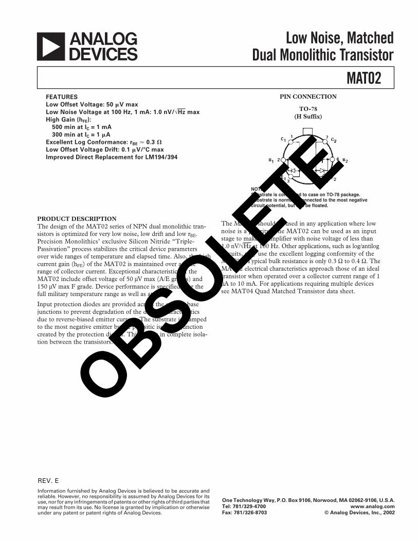
a Low Noise, MatchedDual Monolithic Transistor
MAT02FEATURES
Low Offset Voltage: 50 V max
Low Noise Voltage at 100 Hz, 1 mA: 1.0 nV/√Hz max
High Gain (hFE):
500 min at IC = 1 mA
300 min at IC = 1 A
Excellent Log Conformance: rBE 0.3 Low Offset Voltage Drift: 0.1 V/C max
Improved Direct Replacement for LM194/394
NOTESubstrate is connected to case on TO-78 package.Substrate is normally connected to the most negativecircuit potential, but can be floated.
PIN CONNECTION
TO-78(H Suffix)
PRODUCT DESCRIPTIONThe design of the MAT02 series of NPN dual monolithic tran-sistors is optimized for very low noise, low drift and low rBE.Precision Monolithics’ exclusive Silicon Nitride “Triple-Passivation” process stabilizes the critical device parametersover wide ranges of temperature and elapsed time. Also, the highcurrent gain (hFE) of the MAT02 is maintained over a widerange of collector current. Exceptional characteristics of theMAT02 include offset voltage of 50 µV max (A/E grades) and150 µV max F grade. Device performance is specified over thefull military temperature range as well as at 25°C.
Input protection diodes are provided across the emitter-basejunctions to prevent degradation of the device characteristicsdue to reverse-biased emitter current. The substrate is clampedto the most negative emitter by the parasitic isolation junctioncreated by the protection diodes. This results in complete isola-tion between the transistors.
Information furnished by Analog Devices is believed to be accurate andreliable. However, no responsibility is assumed by Analog Devices for itsuse, nor for any infringements of patents or other rights of third parties thatmay result from its use. No license is granted by implication or otherwiseunder any patent or patent rights of Analog Devices.
One Technology Way, P.O. Box 9106, Norwood, MA 02062-9106, U.S.A.
Tel: 781/329-4700 www.analog.com
Fax: 781/326-8703 © Analog Devices, Inc., 2002
REV. E
The MAT02 should be used in any application where lownoise is a priority. The MAT02 can be used as an inputstage to make an amplifier with noise voltage of less than1.0 nV/√Hz at 100 Hz. Other applications, such as log/antilogcircuits, may use the excellent logging conformity of theMAT02. Typical bulk resistance is only 0.3 Ω to 0.4 Ω. TheMAT02 electrical characteristics approach those of an idealtransistor when operated over a collector current range of 1µA to 10 mA. For applications requiring multiple devicessee MAT04 Quad Matched Transistor data sheet.
OBSOLETE

REV. E–2–
ELECTRICAL CHARACTERISTICS MAT02E MAT02F
Parameter Symbol Conditions Min Typ Max Min Typ Max Unit
Current Gain hFE IC = 1 mA1 500 605 400 605IC = 100 µA 500 590 400 590IC = 10 µA 400 550 300 550IC = 1 µA 300 485 200 485
Current Gain Match ∆hFE 10 µA ≤ IC ≤ 1 mA2 0.5 2 0.5 4 %Offset Voltage VOS VCB = 0, 1 µA ≤ IC ≤ 1 mA3 10 50 80 150 µVOffset Voltage ∆VOS/∆VCB 0 ≤ VCB ≤ VMAX
4 10 25 10 50 µVChange vs. VCB 1 µA ≤ IC ≤ 1 mA3 10 25 10 50 µV
Offset Voltage Change ∆VOS/∆IC VCB = 0 V 5 25 5 50 µVvs. Collector Current 1 µA ≤ IC ≤ 1 mA3 5 25 5 50 µV
Offset CurrentChange vs. VCB ∆IOS/∆VCB 0 ≤ VCB ≤ VMAX 30 70 30 70 pA/V
Bulk Resistance rBE 10 µA ≤ IC ≤ 10 mA5 0.3 0.5 0.3 0.5 ΩCollector-Base
Leakage Current ICBO VCB = VMAX 25 200 25 400 pACollector-Collector
Leakage Current ICC VCC = VMAX5, 6 35 200 35 400 pA
Collector-Emitter VCE = VMAX5, 6
Leakage Current ICES VBE = 0 35 200 35 400 pANoise Voltage Density en IC = 1 mA, VCB = 07
fO = 10 Hz 1.6 2 1.6 3 nV/√Hz fO = 100 Hz 0.9 1 0.9 2 nV/√Hz fO = 1 kHz 0.85 1 0.85 2 nV/√Hz fO = 10 kHz 0.85 1 0.85 2 nV/√Hz
Collector SaturationVoltage VCE(SAT) IC = 1 mA, IB = 100 µA 0.05 0.1 0.05 0.2 V
Input Bias Current IB IC = 10 µA 25 34 nAInput Offset Current IOS IC = 10 µA 0.6 1.3 nABreakdown Voltage BVCEO 40 40 VGain-Bandwidth Product fT IC = 10 mA, VCE = 10 V 200 200 MHzOutput Capacitance COB VCB = 15 V, IE = 0 23 23 pFCollector-Collector
Capacitance CCC VCC = 0 35 35 pF
NOTES1Current gain is guaranteed with Collector-Base Voltage (VCB) swept from 0 to VMAX at the indicated collector currents.2Current gain match (∆hFE) is defined as: ∆hFE =
3Measured at IC = 10 µA and guaranteed by design over the specified range of IC.4This is the maximum change in VOS as VCB is swept from 0 V to 40 V.5Guaranteed by design.6ICC and ICES are verified by measurement of ICBO.7Sample tested.
Specifications subject to change without notice.
100 (∆IB) (hFE min)IC
MAT02–SPECIFICATIONS(@ VCB = 15 V, IC = 10 A, TA = 25C, unless otherwise noted.)
OBSOLETE

ELECTRICAL CHARACTERISTICS MAT02E MAT02F
Parameter Symbol Conditions Min Typ Max Min Typ Max Unit
Offset Voltage VOS VCB = 0 70 220 µV1 µA ≤ IC ≤ 1 mA1
Average OffsetVoltage Drift TCVOS 10 µA ≤ IC ≤ 1 mA, 0 ≤ VCB ≤ VMAX
2 0.08 0.3 0.08 1 µV/°CVOS Trimmed to Zero3 0.03 0.1 0.03 0.3
Input Offset Current IOS IC = 10 µA 8 13 nAInput Offset
Current Drift TCIOS IC = 10 µA4 40 90 40 150 pA/°CInput Bias Current IB IC = 10 µA 45 50 nACurrent Gain hFE IC = 1 mA5 325 300
IC = 100 µA 275 250IC = 10 µA 225 200IC = 1 µA 200 150
Collector-Base ICBO VCB = VMAX 2 3 nALeakage Current
Collector-Emitter ICES VCE = VMAX, VBE = 0 3 4 nALeakage Current
Collector-Collector ICC VCC = VMAX 3 4 nALeakage Current
NOTES1Measured at IC = 10 µA and guaranteed by design over the specified range of IC.
2Guaranteed by VOS test (TCVOS ≅ V
TOS
for VOS VBE) T = 298K for TA = 25°C.
3The initial zero offset voltage is established by adjusting the ratio of IC1 to IC2 at TA = 25°C. This ratio must be held to 0.003% over the entire temperature range.Measurements are taken at the temperature extremes and 25°C.4Guaranteed by design.5Current gain is guaranteed with Collector-Base Voltage (VCB) swept from 0 V to VMAX at the indicated collector current.
Specifications subject to change without notice.
(VCB = 15 V, –25C ≤ TA ≤ +85C, unless otherwise noted.)
MAT02
–3–REV. E
WARNING!
ESD SENSITIVE DEVICE
CAUTIONESD (electrostatic discharge) sensitive device. Electrostatic charges as high as 4000 V readilyaccumulate on the human body and test equipment and can discharge without detection.Although the MAT02 features proprietary ESD protection circuitry, permanent damage mayoccur on devices subjected to high energy electrostatic discharges. Therefore, proper ESDprecautions are recommended to avoid performance degradation or loss of functionality.
ABSOLUTE MAXIMUM RATINGS1
Collector-Base Voltage (BVCBO) . . . . . . . . . . . . . . . . . . . . 40 VCollector-Emitter Voltage (BVCEO) . . . . . . . . . . . . . . . . . . 40 VCollector-Collector Voltage (BVCC) . . . . . . . . . . . . . . . . . . 40 VEmitter-Emitter Voltage (BVEE) . . . . . . . . . . . . . . . . . . . . 40 VCollector Current (IC) . . . . . . . . . . . . . . . . . . . . . . . . . . 20 mAEmitter Current (IE) . . . . . . . . . . . . . . . . . . . . . . . . . . . 20 mATotal Power Dissipation
Case Temperature ≤ 40°C2 . . . . . . . . . . . . . . . . . . . . . 1.8 WAmbient Temperature ≤ 70°C3 . . . . . . . . . . . . . . . . 500 mW
Operating Temperature RangeMAT02E, F . . . . . . . . . . . . . . . . . . . . . . . . . –25°C to +85°C
ORDERING GUIDE
VOS max Temperature PackageModel (TA = 25C) Range Option
MAT02EH 50 µV –25°C to +85°C TO-78MAT02FH 150 µV –25°C to +85°C TO-78
Operating Junction Temperature . . . . . . . . . . –55°C to +150°CStorage Temperature . . . . . . . . . . . . . . . . . . . –65°C to +150°CLead Temperature (Soldering, 60 sec) . . . . . . . . . . . . . 300°CJunction Temperature . . . . . . . . . . . . . . . . . . –65°C to +150°CNOTES1Absolute maximum ratings apply to both DICE and packaged devices.2Rating applies to applications using heat sinking to control case temperature.
Derate linearly at 16.4 mW/°C for case temperature above 40°C.3Rating applies to applications not using a heat sinking; devices in free air only.
Derate linearly at 6.3 mW/°C for ambient temperature above 70°C.OBSOLETE

MAT02
–4– REV. E
TPC 1. Current Gain vs.Collector Current
TPC 4. Base-Emitter-OnVoltage vs. Collector Current
TPC 7. Saturation Voltagevs. Collector Current
TPC 2. Current Gainvs. Temperature
TPC 5. Small Signal InputResistance vs. Collector Current
TPC 8. Noise VoltageDensity vs. Frequency
TPC 3. Gain Bandwidthvs. Collector Current
TPC 6. Small-Signal OutputConductance vs. Collector Current
TPC 9. Noise Voltage Densityvs. Collector Current
–Typical Performance Characteristics
OBSOLETE

MAT02
–5–REV. E
TPC 10. Noise Current Density vs. Frequency
TPC 13. Collector-to-Collector Leakage vs. Temperature
TPC 12. Collector-to-BaseLeakage vs. Temperature
TPC 15. Collector-BaseCapacitance vs. Reverse Bias Voltage
TPC 17. Emitter-Base Capacitance vs. Reverse Bias Voltage
TPC 16. Collector-to-Collector Capacitance vs. Reverse Bias Voltage
TPC 11. Total Noise vs. Collective Current
TPC 14. Collector-to-Collector Capacitance vs. Collector-to Substrate Voltage
OBSOLETE
MAT02
–6– REV. E
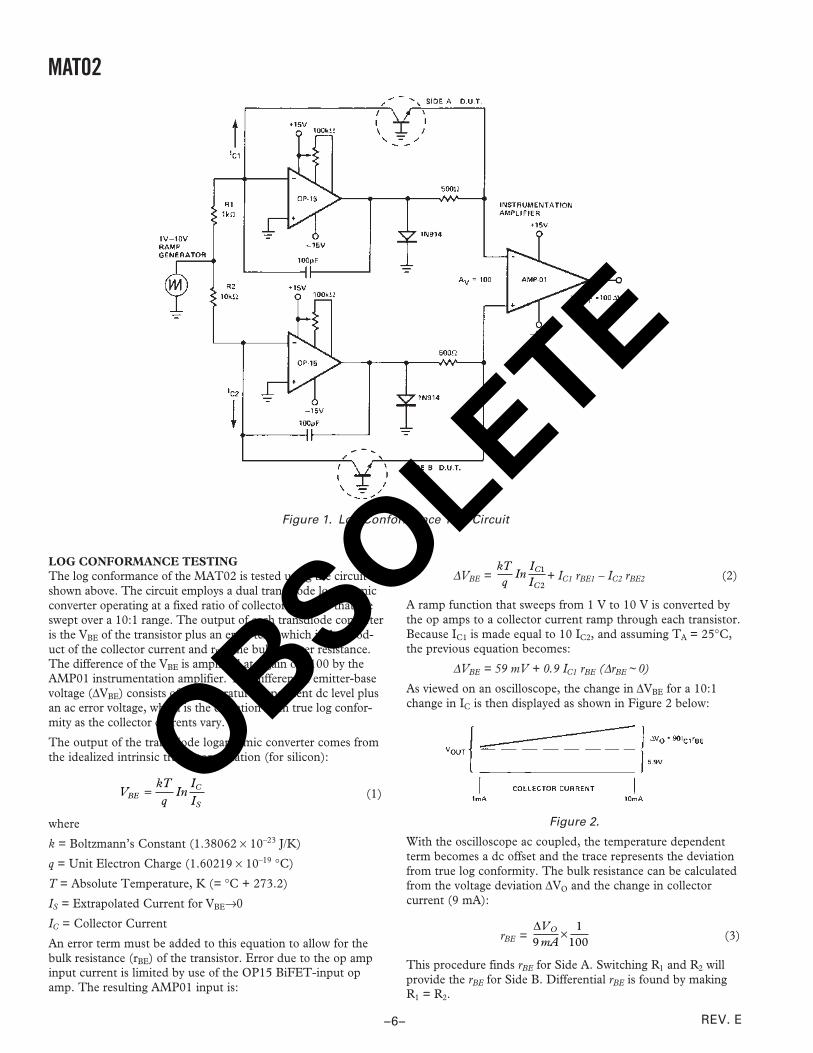
Figure 1. Log Conformance Test Circuit
LOG CONFORMANCE TESTINGThe log conformance of the MAT02 is tested using the circuitshown above. The circuit employs a dual transdiode logarithmicconverter operating at a fixed ratio of collector currents that areswept over a 10:1 range. The output of each transdiode converteris the VBE of the transistor plus an error term which is the prod-uct of the collector current and rBE, the bulk emitter resistance.The difference of the VBE is amplified at a gain of ×100 by theAMP01 instrumentation amplifier. The differential emitter-basevoltage (∆VBE) consists of a temperature-dependent dc level plusan ac error voltage, which is the deviation from true log confor-mity as the collector currents vary.
The output of the transdiode logarithmic converter comes fromthe idealized intrinsic transistor equation (for silicon):
VkTq
InIIBE
C
S= (1)
where
k = Boltzmann’s Constant (1.38062 × 10⁻²³ J/K)
q = Unit Electron Charge (1.60219 × 10⁻¹⁹ °C)
T = Absolute Temperature, K (= °C + 273.2)
IS = Extrapolated Current for VBE→0IC = Collector Current
An error term must be added to this equation to allow for thebulk resistance (rBE) of the transistor. Error due to the op ampinput current is limited by use of the OP15 BiFET-input opamp. The resulting AMP01 input is:
∆VBE =
kTq
InIC1
IC2+ IC1 rBE1 – IC2 rBE2 (2)
A ramp function that sweeps from 1 V to 10 V is converted bythe op amps to a collector current ramp through each transistor.Because IC1 is made equal to 10 IC2, and assuming TA = 25°C,the previous equation becomes:
∆VBE = 59 mV + 0.9 IC1 rBE (∆rBE ~ 0)
As viewed on an oscilloscope, the change in ∆VBE for a 10:1change in IC is then displayed as shown in Figure 2 below:
Figure 2.
With the oscilloscope ac coupled, the temperature dependentterm becomes a dc offset and the trace represents the deviationfrom true log conformity. The bulk resistance can be calculatedfrom the voltage deviation ∆VO and the change in collectorcurrent (9 mA):
rBE =
∆VO
9mA×
1100 (3)
This procedure finds rBE for Side A. Switching R1 and R2 willprovide the rBE for Side B. Differential rBE is found by makingR1 = R2.
OBSOLETE

MAT02
–7–REV. E
Figure 3. One-Quadrant Multiplier/Divider
APPLICATIONS: NONLINEAR FUNCTIONSMULTIPLIER/DIVIDER CIRCUITThe excellent log conformity of the MAT02 over a very widerange of collector current makes it ideal for use in log-antilogcircuits. Such nonlinear functions as multiplying, dividing,squaring and square-rooting are accurately and easily imple-mented with a log antilog circuit using two MAT02 pairs (seeFigure 3). The transistor circuit accepts three input currents (I1,I2 and I3) and provides an output current IO according toIO = I1I2/I3. All four currents must be positive in the log antilogcircuit, but negative input voltages can be easily accommodatedby various offsetting techniques. Protective diodes across eachbase-to-emitter junction would normally be needed, but thesediodes are built into the MAT02. External protection diodesare, therefore, not needed.
For the circuit shown in Figure 3, the operational amplifiersmake I1 = VX/R1, I2 = VY/R2, I3 = VZ/R3, and IO = VO/RO. Theoutput voltage for this one-quadrant, log-antilog multiplier/divider is ideally:
VO =
R3RO
R1R2
V XVY
V Z (VX, VY, VZ > 0) (4)
If all the resistors (RO, R1, R2, R3) are made equal, then
VO = VXVY/VZ
Resistor values of 50 kΩ to 100 kΩ are recommended assumingan input range of 0.1 V to +10 V.
ERROR ANALYSISThe base-to-emitter voltage of the MAT02 in its forward activeoperation is:
VBE =
kTq
InIC
IS + rBEIC, VCB ~ 0 (5)
The first term comes from the idealized intrinsic transistorequation previously discussed (see equation (1)).
Extrinsic resistive terms and the early effect cause departurefrom the ideal logarithmic relationship. For small VCB, all of
these effects can be lumped together as a total effective bulkresistance rBE. The rBEIC term causes departure from the desiredlogarithmic relationship. The rBE term for the MAT02 is lessthan 0.5 Ω and ∆rBE between the two sides is negligible.
Returning to the multiplier/divider circuit of Figure 1 and usingEquation (4):
VBE1A + VBE2A – VBE2B – VBE1B + (I1 + I2 – IO – I3) rBE = 0
If the transistor pairs are held to the same temperature, then:
kTq
In I II I
kTq
In I II IO
S A S A
S B S B
1 2
3
1 2
1 2= + (I1 + I2 – IO – I3) rBE (6)
If all the terms on the right-hand side were zero, then In(I1 I2/I3 IO) would equal zero, which would lead directly tothe desired result:
IO =
I1I2
I3, where I1, I2, I3, IO > 0 (7)
Note that this relationship is temperature independent. Theright-hand side of Equation (6) is near zero and the outputcurrent IO will be approximately I1 I2/I3. To estimate error,define ø as the right-hand side terms of Equation (6):
ø = In
I II I
qkT
S A S A
S B S B
1 2
1 2+ (I1 + I2 – IO – I3) rBE (8)
For the MAT02, In (ISA/ISB) and ICrBE are very small. For smallø, εØ ~ 1 + ø and therefore:
I1I2
I3IO = 1 + ø
(9)
IO ~
I1I2
I3 (1 – ø)
The In (ISA/ISB) terms in ø cause a fixed gain error of less than±0.6% from each pair when using the MAT02, and this gainerror is easily trimmed out by varying RO. The IOUT terms are
OBSOLETE

MAT02
–8– REV. E
more troublesome because they vary with signal levels and aremultiplied by absolute temperature. At 25°C, kT/q isapproximately 26 mV and the error due to an rBEIC term will berBEIC/26 mV. Using an rBE of 0.4 Ω for the MAT02 and assum-ing a collector current range of up to 200 µA, then a peak errorof 0.3% could be expected for an rBEIC error term when usingthe MAT02. Total error is dependent on the specific applicationconfiguration (multiply, divide, square, etc.) and the requireddynamic range. An obvious way to reduce ICrBE error is to re-duce the maximum collector current, but then op amp offsetsand leakage currents become a limiting factor at low input lev-els. A design range of no greater than 10 µA to 1 mA is generallyrecommended for most nonlinear function circuits.
A powerful technique for reducing error due to ICrBE is shown inFigure 4. A small voltage equal to ICrBE is applied to the transis-tor base. For this circuit:
VB =
RC
R2 V1 and ICrBE =
rBE
R1 V1 (10)
The error from rBEIC is cancelled if RC/R2 is made equal to rOUT R1.Since the MAT02 bulk resistance is approximately 0.39 Ω, anRC of 3.9 Ω and R2 of 10 R1 will give good error cancellation.
In more complex circuits, such as the circuit in Figure 3, it maybe inconvenient to apply a compensation voltage to each indi-vidual base. A better approach is to sum all compensation to thebases of Q1. The “A” side needs a base voltage of (VO/RO + VZ/R3) rBE, and the “B” side needs a base voltage of (VX/R1+VY/R2)rBE. Linearity of better than ±0.1% is readily achievable withthis compensation technique.
Operational amplifier offsets are another source of error. InFigure 4, the input offset voltage and input bias current willcause an error in collector current of (VOS/R1) + IB. A lowoffset op amp, such as the OP07 with less than 75 µV of VOS
and IB of less than ± 3 nA, is recommended. The OP193,micropower op amp, should be considered if low power con-
sumption or single-supply operation is needed. The value offrequency-compensating capacitor (CO) is dependent on theop amp frequency response and peak collector current. Typi-cal values for CO range from 30 pF to 300 pF.
Figure 4. Compensation of Bulk Resistance Error
FOUR-QUADRANT MULTIPLIERA simplified schematic for a four-quadrant log-antilog multiplieris shown in Figure 5. Similar to the previously discussed one-quadrant multiplier, the circuit makes IO = I1 I2/I3. The twoinput currents, I1 and I2, are each offset in the positive direction.This positive offset is then subtracted out at the output stage.Assuming ideal op amps, the currents are:
I V
RVR
I VR
VR
X R Y R1
1 22
1 2= + = +,
(11)
I V
RVR
VR
VR
I VRO
X Y R O
O
R= + + + =1 1 2
32
,
From IO = I1 I2/I3, the output voltage will be:
VO =
ROR2
R12
V XVY
V R(12)
Figure 5. Four-Quadrant Multiplier
OBSOLETE

MAT02
–9–REV. E
Collector current range is the key design decision. The inher-ently low rBE of the MAT02 allows the use of a relatively highcollector current. For input scaling of ±10 V full-scale and usinga 10 V reference, we have a collector-current range for I1 and I2
of:
–10 10 10 101 2 1 2R R
IR RC+
≤ ≤ +
(13)
Practical values for R1 and R2 would range from 50 kΩ to100 kΩ. Choosing an R1 of 82 kΩ and R2 of 62 kΩ provides acollector current range of approximately 39 µA to 283 µA. AnRO of 108 kΩ will then make the output scale factor 1/10 andVO = VXVY/10. The output, as well as both inputs, are scaled for±10 V full scale.
Linear error for this circuit is substantially improved by thesmall correction voltage applied to the base of Q1 as shown inFigure 5. Assuming an equal bulk emitter resistance for eachMAT02 transistor, then the error is nulled if:
(I1 + I2 – I3 – IO) rBE + ρVO = 0
The currents are known from the previous discussion, and therelationship needed is simply:
VO =
rBE
RO VO (14)
The output voltage is attenuated by a factor of rBE/RO and ap-plied to the base of Q1 to cancel the summation of voltage dropsdue to rBEIC terms. This will make In (I1 I2/I3 IO) more nearlyzero which will thereby make IO = I1 I2/I3 a more accurate rela-tionship. Linearity of better than 0.1% is readily achievable withthis circuit if the MAT02 pairs are carefully kept at the sametemperature.
Figure 6. Multifunction Converter
MULTIFUNCTION CONVERTERThe multifunction converter circuit provides an accurate meansof squaring, square rooting, and raising ratios to arbitrary pow-ers. The excellent log conformity of the MAT02 allows a widerange of exponents. The general transfer function is:
VO = VY
V Z
V X
m
(15)
VX, VY, and VZ are input voltages and the exponent “m” has apractical range of approximately 0.2 to 5. Inputs VX and VY areoften taken from a fixed reference voltage. With a REF01 pro-viding a precision 10 V to both VX and VY, the transfer functionwould simplify to:
VO = 10
V Z
10
m
(16)
As with the multiplier/divider circuits, assume that the transistorpairs have excellent matching and are at the same temperature.The In ISA/ISB will then be zero. In the circuit of Figure 6, thevoltage drops across the base-emitter junctions of Q1 provide:
RB
RB + KRAV A =
kTq
InIZ
IX(17)
IZ is VZ/R1 and IX is VX/R1. Similarly, the relationship for Q2 is:
RB
RB + 1– K( )RAV A =
kTq
InIO
I Y(18)
IO is VO/RO and IY is VY/R1. These equations for Q1 and Q2 canthen be combined.
RB + KRA
RB + 1– K( )RAIn
IZ
IX= In
IO
IY(19)
OBSOLETE

MAT02
–10– REV. E
Substituting in the voltage relationships and simplifying leadsto:
VO =
RO
R1VY
V Z
V X
m
, where
(20)
m =
RB + KRA
RB + 1– K( ) RA
The factor “K” is a potentiometer position and varies from zeroto 1.0, so “m” ranges from RB/(RA + RB) to (RB + RA)/RB.Practical values are 125 Ω for RB and 500 Ω for RA; thesevalues will provide an adjustment range of 0.2 to 5.0. A valueof 100 kΩ is recommended for the R1 resistors assuming a full-scale input range of 10 V. As with the one-quadrantmultiplier/divider circuit previously discussed, the VX, VY, andVZ inputs must all be positive.
The op amps should have the lowest possible input offsets. TheOP07 is recommended for most applications, although suchprogrammable micropower op amps as the OP193/OP293 offeradvantages in low-power or single-supply circuits. The micro-power op amps also have very low input bias-current drift, animportant advantage in log/antilog circuits. External offsetnulling may be needed, particularly for applications requiring awide dynamic range. Frequency compensating capacitors, onthe order of 50 pF, may be required for A2 and A3. AmplifierA1 is likely to need a larger capacitor, typically 0.0047 µF, toassure stability.
Accuracy is limited at the higher input levels by bulk emitterresistance, but this is much lower for the MAT02 than for othertransistor pairs. Accuracy at the lower signal levels primarilydepends on the op amp offsets. Accuracies of better than 1%are readily achievable with this circuit configuration and can bebetter than ±0.1% over a limited operating range.
FAST LOGARITHMIC AMPLIFIERThe circuit of Figure 7 is a modification of a standard logarith-mic amplifier configuration. Running the MAT02 at 2.5 mAper side (full-scale) allows a fast response with wide dynamicrange. The circuit has a 7 decade current range, a 5 decadevoltage range, and is capable of 2.5 µs settling time to 1% witha 1 V to 10 V step.
The output follows the equation:
VO =
R3 + R2
R2
kTq
InV REF
V IN(21)
The output is inverted with respect to the input, and is nomi-nally –1 V/decade using the component values indicated.
Figure 7. Fast Logarithmic Amplifier
LOW-NOISE 1000 AMPLIFIERThe MAT02 noise voltage is exceptionally low, only 1 nV/√Hzat 10 Hz when operated over a collector current range of 1 mAto 4 mA. A single-ended ×1000 amplifier that takes advantage ofthis low MAT02 noise level is shown in Figure 8. In addition tolow noise, the amplifier has very low drift and high CMRR. AnOP184 is used for the second stage to obtain good speed withminimal power consumption. Small-signal bandwidth is 4.0MHz, slew rate is 2.4 V/µs, and total supply current is approxi-mately 2.25 mA.
Figure 8. Low-Noise, Single-Ended × 1000 Amplifier
OBSOLETE

MAT02
–11–REV. E
Transistors Q2 and Q3 form a 2 mA current source (0.65 V/330 Ω ~ 2 mA). Each collector of Q1 operates at 1 mA. TheOP184 inputs are 3 V below the positive supply voltage (RLIC
~ 3 V). Input stage gain is gmRL, which is approximately 100when operating at IC of 1 mA with RL of 3 kΩ. Since theOP184 has a minimum open-loop gain of 500,000, totalopen-loop gain for the composite amplifier is over 50 million.Even at closed-loop gain of 1000, the gain error due to finiteopen-loop gain will be negligible. The OP184 features excellentsymmetry of slew-rate and very linear gain. Signal distortion isminimal.
Dynamic range of this amplifier is excellent; the OP184 has anoutput voltage swing of ±14.8 V with a ±15 V supply.
Input characteristics are outstanding. The MAT02F has offsetvoltage of less than 150 µV at 25°C and a maximum offset driftof 1 µV/°C. Nulling the offset will further reduce offset drift.This can be accomplished by slightly unbalancing the collectorload resistors. This adjustment will reduce the drift to less than0.1 µV/°C.
Input bias current is relatively low due to the high current gainof the MAT02. The minimum β of 400 at 1 mA for theMAT02F implies an input bias current of approximately 2.5 µA.This circuit should be used with signals having relatively lowsource impedance. A high source impedance will degrade offsetand noise performance.
This circuit configuration provides exceptionally low input noisevoltage and low drift. Noise can be reduced even further byraising the collector currents from 1 mA to 3 mA, but powerconsumption is then increased.
OBSOLETE
MAT02
–12– REV. E
C00
283–
0–4/
02(E
)P
RIN
TE
D IN
U.S
.A.
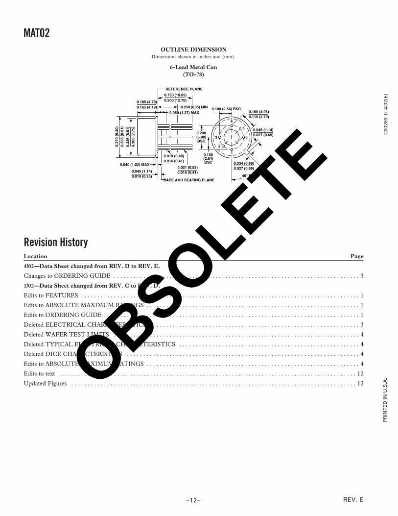
OUTLINE DIMENSIONDimensions shown in inches and (mm).
6-Lead Metal Can(TO-78)
0.250 (6.35) MIN
0.750 (19.05) 0.500 (12.70)0.185 (4.70)
0.165 (4.19)
REFERENCE PLANE
0.050 (1.27) MAX
0.019 (0.48)0.016 (0.41)
0.021 (0.53)0.016 (0.41)0.045 (1.14)
0.010 (0.25)
0.040 (1.02) MAX
BASE AND SEATING PLANE
0.33
5 (8
.51)
0.30
5 (7
.75)
0.37
0 (9
.40)
0.33
5 (8
.51)
0.034 (0.86)0.027 (0.69)
0.045 (1.14)0.027 (0.69)
0.160 (4.06)0.110 (2.79)
0.100 (2.54) BSC
5
2
6
4
3
1
0.200(5.08)BSC
0.100(2.54)BSC
45° BSC
Revision HistoryLocation Page
4/02—Data Sheet changed from REV. D to REV. E.
Changes to ORDERING GUIDE . . . . . . . . . . . . . . . . . . . . . . . . . . . . . . . . . . . . . . . . . . . . . . . . . . . . . . . . . . . . . . . . . . . . . . . . . . . 3
1/02—Data Sheet changed from REV. C to REV. D.
Edits to FEATURES . . . . . . . . . . . . . . . . . . . . . . . . . . . . . . . . . . . . . . . . . . . . . . . . . . . . . . . . . . . . . . . . . . . . . . . . . . . . . . . . . . . . . 1
Edits to ABSOLUTE MAXIMUM RATINGS . . . . . . . . . . . . . . . . . . . . . . . . . . . . . . . . . . . . . . . . . . . . . . . . . . . . . . . . . . . . . . . . . 1
Edits to ORDERING GUIDE . . . . . . . . . . . . . . . . . . . . . . . . . . . . . . . . . . . . . . . . . . . . . . . . . . . . . . . . . . . . . . . . . . . . . . . . . . . . . . 1
Deleted ELECTRICAL CHARACTERISTICS . . . . . . . . . . . . . . . . . . . . . . . . . . . . . . . . . . . . . . . . . . . . . . . . . . . . . . . . . . . . . . . . 3
Deleted WAFER TEST LIMITS . . . . . . . . . . . . . . . . . . . . . . . . . . . . . . . . . . . . . . . . . . . . . . . . . . . . . . . . . . . . . . . . . . . . . . . . . . . 4
Deleted TYPICAL ELECTRICAL CHARACTERISTICS . . . . . . . . . . . . . . . . . . . . . . . . . . . . . . . . . . . . . . . . . . . . . . . . . . . . . . . 4
Deleted DICE CHARACTERISTICS . . . . . . . . . . . . . . . . . . . . . . . . . . . . . . . . . . . . . . . . . . . . . . . . . . . . . . . . . . . . . . . . . . . . . . . 4
Edits to ABSOLUTE MAXIMUM RATINGS . . . . . . . . . . . . . . . . . . . . . . . . . . . . . . . . . . . . . . . . . . . . . . . . . . . . . . . . . . . . . . . . . 4
Edits to text . . . . . . . . . . . . . . . . . . . . . . . . . . . . . . . . . . . . . . . . . . . . . . . . . . . . . . . . . . . . . . . . . . . . . . . . . . . . . . . . . . . . . . . . . . . 12
Updated Figures . . . . . . . . . . . . . . . . . . . . . . . . . . . . . . . . . . . . . . . . . . . . . . . . . . . . . . . . . . . . . . . . . . . . . . . . . . . . . . . . . . . . . . . 12OBSOLETE