Embed Size (px)
Citation preview
Low Power, Low Area, Monolithic Oversampling
Digital to Analog Conversionby
Edward A. KeehrSubmitted to the Department of Electrical Engineering and Computer
Sciencein partial fulfillment of the requirements for the degree of
Master of Engineering in Electrical Engineering and Computer Science
at theMASSACH
MASSACHUSETTS INSTITUTE OF TECHNOLOGY OFi
September 2002 JUL
© Edward A. Keehr, MMII. All rights reserved. L
The author hereby grants to MIT permission to reproduce anddistribute publicly paper and electronic copies of this thesis document sAR~qM
in whole or in part.
Author .............................. ...........
Department of Electrical Engineering and Computer ScienceJune 19, 2002
Certified by......................James K. Roberge
Professor of Electrical Engineering-- '-Thesis Supervisor
C ertified by ........................ ........Sean J. Wang
S ior Engineer,.Qu lcomm, Inc.Ths'j pvisor
Accepted by......................Arthur C. Smith
Chairman, Department Committee on Graduate Students
USETTS INTITUTEECHNOLOGY
3 1 2002
BRARIES
Low Power, Low Area, Monolithic Oversampling Digital to
Analog Conversion
by
Edward A. Keehr
Submitted to the Department of Electrical Engineering and Computer Scienceon June 19, 2002, in partial fulfillment of the
requirements for the degree ofMaster of Engineering in Electrical Engineering and Computer Science
Abstract
This thesis project examines the design of a monolithic audio-band digital-to-analog(D/A) converter with the objective of achieving a high signal-to-noise ratio, low ana-log die area consumption, and low static power dissipation. Issues relating to systemdesign, digital signal processing, sigma-delta modulation, D/A topology selection,and switched-capacitor filter design are covered. The Direct Charge Transfer filteringtechnique in particular is analyzed in detail, confirming its suitability and superiorityover traditional switched-capacitor filtering techinques for the given project require-nents. The end result of this project was the design of a D/A converter that achievedan SNR of 92dB with an analog die area consumption of 0.187mm 2 and a static powerdissipation of 2.2mW in a 0.25pm CMOS process with a 2.5V supply voltage.
Thesis Supervisor: James K. RobergeTitle: Professor of Electrical Engineering
Thesis Supervisor: Sean J. WangTitle: Senior Engineer, Qualcomm, Inc.
2
Acknowledgments
I wish to acknowledge the support and the assistance of the many people both at Qual-
comm, Inc. and the Massachusetts Institute of Technology that contributed to this
thesis and made this project a professional and academic experience beyond compare.
First, I would like to acknowledge the support of my friend and direct project su-
pervisor Sean Wang, who provided countless hours of mentoring in order to help me
make the leap from the textbook to real world design. As a supervisor, Sean struck
a keen balance between pointing my project in the right direction and providing key
design hints where necessary, while constantly forcing me to question my work such
that I obtained a deeper understanding of what I was doing than would have other-
wise been the case.
I would like to acknowledge the support of Seyfi Bazarjani, who took a chance by
selecting me to run this project and who provided invaluable assistance in helping me
surmount my initial hurdles in understanding sigma-delta modulation and simulation
of sigma-delta modulators.
I would like to acknowledge the support of Levent Aydin, who explained the
system-level aspects of D/A converters and whose sigma-delta modulator simulation
I built upon to produce the system-level simulation of my choice of D/A architecture.
Levent also provided invaluable advice with respect to the postfilter droop compen-
sation technique used in the interpolation filtering chain.
I would like to acknowledge Samir Gupta's keen and well-timed interjection that
the number of interpolation filter taps was "not an issue".
Finally, I would like to acknowledge Professor James Roberge, who accepted the
3

duty of reading this report and who provided the final word on several debates sur-
rounding this project.
4
Contents
1 Introduction
1.1 M otivation . . . . . . . . . . . . . . . . . . . . . . . . . . . . . . . . .
1.2 O bjective . . . . . . . . . . . . . . . . . . . . . . . . . . . . . . . . .
2 D/A Conversion Overview
2.1 General D/A Conversion Procedure . . . . . . . . . . . . . . . . . . .
2.1.1 D/A Code Topologies . . . . . . . . . . . . . . . . . . . . . . .
2.1.2 D/A Medium Topologies . . . . . . . . . . . . . . . . . . . . .
2.1.3 Discrete Time - Continuous Time Interface . . . . . . . . . . .
2.1.4 Analog Postfiltering . . . . . . . . . . . . . . . . . . . . . . . .
2.2 Nyquist Converters . . . . . . . . . . . . . . . . . . . . . . . . . . . .
2.3 Oversampling D/A Converters . . . . . . . . . . . . . . . . . . . . . .
2.3.1 Sigma-Delta Modulator Concepts . . . . . . . . . . . . . . . .
2.3.2 Analog Postfilter . . . . . . . . . . . . . . . . . . . . . . . . .
2.4 D/A Converter Metrics . . . . . . . . . . . . . . . . . . . . . . . . . .
2.4.1 Static Metrics . . . . . . . . . . . . . . . . . . . . . . . . . . .
2.4.2 Frequency Domain Metrics .
2.5 Oversampling D/A Optimization Strategies
2.5.1 Gain and Noise . . . . . . . . . . . .
2.5.2 Linearity and Overload . . . . . . . .
5
13
13
14
16
17
17
19
20
21
22
24
28
31
33
33
35
37
37
38
.
.
.
.
3 Digital Interpolation and Noise Shaping 40
3.1 Digital Quantization Noise . . . . . . . . . . . . . . . . . . . . . . . . 41
3.1.1 Uniform Quantization . . . . . . . . . . . . . . . . . . . . . . 41
3.1.2 Quantization Noise Linearization Approximation . . . . . . . . 44
3.1.3 Calculation of Quantization Noise Power . . . . . . . . . . . . 46
3.1.4 Quantization Noise Power with Oversampling . . . . . . . . . 47
3.2 Digital Interpolation Filtering . . . . . . . . . . . . . . . . . . . . . . 49
3.2.1 Upsampling . . . . . . . . . . . . . . . . . . . . . . . . . . . . 49
3.2.2 FIR Image-Reject Filtering . . . . . . . . . . . . . . . . . . . . 51
3.2.3 Multistage Interpolation . . . . . . . . . . . . . . . . . . . . . 54
3.2.4 Postfilter Droop Correction . . . . . . . . . . . . . . . . . . . 58
3.2.5 Digital Zero Order Hold Interpolation . . . . . . . . . . . . . . 62
3.3 Sigma-Delta Noise Shaping . . . . . . . . . . . . . . . . . . . . . . . . 63
3.3.1 Advantage of Multi-Order Sigma-Delta Modulation . . . . . . 65
3.3.2 Single Bit vs. Multibit Modulation . . . . . . . . . . . . . . . 68
3.3.3 Implementation of a Sigma-Delta Modulator . . . . . . . . . . 70
3.3.4 Alternative Architectures . . . . . . . . . . . . . . . . . . . . . 77
4 Oversampled D/A Converter Topologies
4.1 Current-Mode Topologies . . . . . . . . . . . . . . . . . . . . . . . . .
4.1.1 Calibrated Current-Mode Topologies . . . . . . . . . . . . . .
4.1.2 Current Mode with Dynamic Element Matching . . . . . . . .
4.1.3 Current Mode Semidigital Filter . . . . . . . . . . . . . . . . .
4.2 Switched-Capacitor D/A and Postfilter Topologies . . . . . . . . . . .
4.2.1 Calibrated Switched-Capacitor Topology . . . . . . . . . . . .
4.2.2 Pseudo-Passive Serial D/A Converter . . . . . . . . . . . . . .
4.2.3 Switched-Capacitor with Dynamic Element Matching and Di-
rect Charge Transfer . . . . . . . . . . . . . . . . . . . . . . .
4.3 Dynamic Element Matching Techniques . . . . . . . . . . . . . . . . .
81
82
83
90
93
96
97
102
112
114
6
4.3.1 Random Element Selection . . . . . . . . . . . . . . . . . . . . 115
4.3.2 Data Weighted Averaging . . . . . . . . . . . . . . . . . . . . 117
4.3.3 Implementation of DWA Circuitry . . . . . . . . . . . . . . . . 120
4.4 Clock Jitter at the DT-CT Interface . . . . . . . . . . . . . . . . . . . 122
5 Switched-Capacitor Postfiltering 125
5.1 Switched-Capacitor Theory . . . . . . . . . . . . . . . . . . . . . . . 126
5.1.1 Switched-Capacitor/Resistor Equivalence . . . . . . . . . . . . 126
5.1.2 Equivalent Resistor-Capacitor/Switched-Capacitor Circuits . . 127
5.1.3 Switched-Capacitor Design Considerations . . . . . . . . . . . 129
5.1.4 Direct Charge Transfer . . . . . . . . . . . . . . . . . . . . . . 138
5.1.5 Correlated Double Sampling . . . . . . . . . . . . . . . . . . . 143
5.1.6 Correlated Double Sampling and the DCT Technique . . . . . 146
5.2 Switched-Capacitor Lowpass Filters . . . . . . . . . . . . . . . . . . . 148
5.2.1 Switched-Capacitor Biquad Filter Analysis . . . . . . . . . . . 149
5.2.2 Direct Charge Transfer Filter Analysis . . . . . . . . . . . . . 155
5.3 Opamp Design for Switched-Capacitor Filters . . . . . . . . . . . . . 157
5.3.1 Topology Choice . . . . . . . . . . . . . . . . . . . . . . . . . 157
5.3.2 Assigning Overdrive Voltages to Key Transistors . . . . . . . . 158
5.3.3 G ain . . . . . . . . . . . . . . . . . . . . . . . . . . . . . . . . 160
5.3.4 Bandwidth . . . . . . . . . . . . . . . . . . . . . . . . . . . . . 161
5.3.5 Phase M argin . . . . . . . . . . . . . . . . . . . . . . . . . . . 161
5.3.6 Input-Referred Noise . . . . . . . . . . . . . . . . . . . . . . . 164
5.4 Hand Design for Noise Budget . . . . . . . . . . . . . . . . . . . . . . 167
5.4.1 Switched-Capacitor Noise Contributions . . . . . . . . . . . . 168
5.4.2 Input Current and Opamp Noise Power . . . . . . . . . . . . . 169
5.4.3 Output Load and Output Stage Current . . . . . . . . . . . . 171
5.4.4 Power/Area Comparison . . . . . . . . . . . . . . . . . . . . . 173
7
6 Analog Postfilter Implementation and Simulation Results
6.1 Analog Implementation ......................
6.1.1 Architectural Considerations . . . . . . . . . . .
6.1.2 Opamp Device Sizing and DC Operating Point
6.1.3 CMOS Switch Sizes . . . . . . . . . . . . . . . .
6.1.4 Clock Generator . . . . . . . . . . . . . . . . .
6.2 Circuit Simulation . . . . . . . . . . . . . . . . . . . .
6.2.1 Differential AC Performance . . . . . . . . . . .
6.2.2 Common Mode Feedback Loop AC Performance
6.2.3 Transient Simulation Results . . . . . . . . . . .
6.2.4 Final Noise Calculations . . . . . . . . . . . . .
6.2.5 Final Power and Area Calculation Results . . .
. . . . . . . . 175
. . . . . . . . 175
. . . . . . . . 182
. . . . . . . . 183
. . . . . . . . 184
. . . . . . . . 186
. . . . . . . . 186
. . . . . . . . 190
. . . . . . . . 192
. . . . . . . . 193
. . . . . . . . 195
7 Conclusion
7.1 Sum m ary . . . . . . . . . . . . . . . . . . . . . . . . . . . . . . . .
7.2 Recommendations for Further Investigation . . . . . . . . . . . . .
196
196
197
8
175
List of Figures
2-1 Block Diagram of Generic D/A Converter . . . . . . . . . . . . . . . 17
2-2 Signal Spectra of Nyquist Converter after DT-CT Conversion . . . . . 23
2-3 Oversampling D/A Converter Block Diagram . . . . . . . . . . . . . 25
2-4 Signal Spectra at Various Points in the Oversampling D/A Converter 26
2-5 Analog Postfilter Image Reject Requirements for Oversampling Con-
verters . . . . . . . . . . . . . . . . . . . . . . . . . . . . . . . . . . . 27
2-6 Sigma-Delta Modulator Concept . . . . . . . . . . . . . . . . . . . . . 29
2-7 Sigma-Delta Modulator Block Diagram . . . . . . . . . . . . . . . . 30
2-8 Oversampling Advantage . . . . . . . . . . . . . . . . . . . . . . . . . 31
2-9 Non-ideal D/A Converter Transfer Function . . . . . . . . . . . . . . 33
2-10 Effect of Gain Positioning on System Noise Performance . . . . . . . 38
3-1 Input/Output Relation and Input/Error Relation for a Uniform Quan-
tizer . . . . . . . . . . . . . . . . . . . . . . . . . . . . . . . . . . . . 42
3-2 Theoretical Quantizer Output Error Probability Density Function . . 45
3-3 16 Bit Quantization Error Power Spectral Density for Sinusoidal Input 46
3-4 Discrete-Time and Frequency Domain Depictions of Upsampling . . . 51
3-5 Digital Implementation of FIR Interpolation Filter . . . . . . . . . . 52
3-6 Multistage Interpolation Block Diagram . . . . . . . . . . . . . . . . 54
3-7 Generic PSD for Consecutive Upsamplings by 2 and Interpolation . . 55
3-8 SNR Degradation in Multistage Interpolation Filtering . . . . . . . . 58
3-9 Filter Droop Compensation on the Complex Z-Plane . . . . . . . . . 59
9
3-10
3-11
3-12
3-13
3-14
3-15
3-16
3-17
3-18
3-19
3-20
3-21
3-22
4-1 Fully Differential Current to Voltage Conversion with Filtering
Calibrated Current-Mode DAC Element . . . . .
Current Mode Semidigital Filter Block Diagram .
Current Mode Semidigital Filter . . . . . . . . . .
Switched-Capacitor Calibration Technique . . . .
Pseudo-Passive Serial D/A Converter . . . . . . .
Serial DAC FIR Reconstruction Filter . . . . . .
Direct-Charge Transfer Concept . . . . . . . . . .
Four-bit SC D/A Converter with DCT Postfilter .
Dynamic Element Matching Concept . . . . . . .
Conceptual Operation of DWA Algorithm . . . .
DFT of DWA Mismatch Error Noise . . . . . . .
. . . . . . . . 85
. . . . . . . . 93
. . . . . . . . 95
. . . . . . . . 97
. . . . . . . . 102
. . . . . . . . 104
. . . . . . . . 113
. . . . . . . . 114
. . . . . . . . 116
. . . . . . . . 118
. . . . . . . . 119
SNR Measurements for DWA from MATLAB Behavioral Simulation
Behavioral Description of DWA Algorithm . . . . . . . . . . . . . .
120
121
10
Signal Band Frequency Response of Compensating Filter . . . . . . .
Frequency Response of D/A Converter Chain with Compensating Filter
Discrete Time Operation of Digital Zero Order Hold . . . . . . . . . .
Block Diagram of Generic D/A Converter . . . . . . . . . . . . . . .
Theoretical Power Spectral Density Functions for Lth Order Modula-
tors with 1-bit Quantization . . . . . . . . . . . . . . . . . . . . . . .
Maximum Amplitude of Input Sinusoid, as Fraction of Digital Full Scale
Behavioral Model of Second Order Sigma-Delta Modulator . . . . . .
Simulated Postfilter Output-Referred In-band SQNR . . . . . . . . .
Quantization Noise Spectrum at Output of D/A Converter . . . . . .
Waveform at Output of D/A Converter . . . . . . . . . . . . . . . . .
Quantization Noise Spectrum at Output of Postfilter . . . . . . . . .
Gate Level Implementation of Second Order Sigma-Delta Modulator .
Error Feedback Modulator Structure . . . . . . . . . . . . . . . . . .
63
64
64
65
67
71
72
74
75
76
78
79
80
83
4-2
4-3
4-4
4-5
4-6
4-7
4-8
4-9
4-10
4-11
4-12
4-13
4-14
4-15 Digital Circuitry Implementation of DWA Algorithm . . . . . .
4-16 Effect of Clock Jitter on a Multi-Level DT-CT Zero Order Hold
5-1 Switched-Capacitor Equivalence with Resistor . . . . . . . . . .
5-2 First Order Active-RC Lowpass Filter . . . . . . . . . . . . . . .
5-3 First Order Switched Capacitor Filter . . . . . . . . . . . . . . .
5-4 Switched Capacitor Noise Derivation . . . . . . . . . . . . . . .
5-5 Clock Switching Scheme to Reduce Distortion . . . . . . . . . .
5-6 Direct Charge Transfer . . . . . . . . . . . . . . . . . . . . . . .
5-7 Direct Charge Transfer Over Process Variation . . . . . . . . . .
5-8 Direct Charge Transfer Parasitic Insensitivity . . . . . . . . . .
5-9 Direct Charge Transfer Noise Analysis . . . . . . . . . . . . . .
5-10 Correlated Double Sampling for a Switched-Capacitor Integrator
5-11 Correlated Double Sampling for Direct Charge Transfer . . . . .
5-12 Correlated Double Sampling SWITCAP Simulation for DCT . .
5-13 Switched-Capacitor Low Q Lowpass Biquad Filter . . . . . . . .
5-14 Schematic of Two-Stage Miller Compensated Opamp . . . . . .
6-1
6-2
6-3
6-4
6-5
6-6
6-7
122
. . . 123
. . . 126
. . . 128
. . . 129
. . . 130
. . . 134
. . . 139
. . . 140
. . . 141
. . . 142
. . . 144
. . . 146
. . . 149
. . . 152
. . . 159
Cadence Schematic of DCT Postfilter . . . . . . . . . . . . . . . . . .
Hand Drawn Schematic of DCT Postfilter . . . . . . . . . . . . . . .
Switched-Capacitor Common Mode Feedback Averaging Circuit . . .
Clock Generation Circuitry Schematic . . . . . . . . . . . . . . . . .
D/A Converter Capacitor Array Switch Timing Diagram . . . . . . .
AC Performance for Opamp 1 Swept Over Differential Output Swing
AC Performance for Opamp 2 Swept Over Differential Output Swing
11
176
177
181
185
187
189
190
List of Tables
2.1 Binary and Thermometer Digital Code Representations . . . . . . . . 18
3.1 Common Signal Digital Number Representations . . . . . . . . . . . . 43
3.2 Peak SQNR for Various OSR/Bit Combinations . . . . . . . . . . . . 72
6.1 Opamp 1 Device Sizes . . . . . . . . . . . . . . . . . . . . . . . . . . 183
6.2 Opamp 2 Device Sizes . . . . . . . . . . . . . . . . . . . . . . . . . . 184
6.3 Sw itch Sizes . . . . . . . . . . . . . . . . . . . . . . . . . . . . . . . . 184
6.4 Waveform Metrics for Clock Generation Circuitry . . . . . . . . . . . 186
6.5 AC Performance for Opamp 1, Beta=0.7 for Phase 2 . . . . . . . . . 188
6.6 AC Performance for Opamp 2, Beta=0.66 for Phase 1 . . . . . . . . . 188
6.7 AC-CMFB Performance for Opamp 1 . . . . . . . . . . . . . . . . . . 191
6.8 AC-CMFB Performance for Opamp 2 . . . . . . . . . . . . . . . . . . 191
6.9 Settling Performance for DCT/CDS Postfilter . . . . . . . . . . . . . 193
12
Chapter 1
Introduction
1.1 Motivation
During the course of the last two decades, digital systems have found their way into
every corner of human civilization. The speed and robustness of digital technology
has led to its replacement of analog technologies and to the development of wholly
digital systems. Of current relevance to today's economy is the prevalence of digi-
tal mobile communications systems. Digital signal processing techniques allow us to
compress and encode the human voice in such a way as to vastly increase the capacity
of our communication networks. The robustness of digital signal transmissions allows
us to reduce the power requirements of such systems, resulting in ever smaller and
cheaper mobile communications systems.
Despite the power of digital systems, the fact remains that the world around us
is analog in nature, and thus signals between the two domains must be converted
from one to another. Hence, at the endpoints of any digital system, we find either an
analog-to-digital (A/D) or a digital-to-analog (D/A) converter providing the interface
from the analog world to the digital domain. Although the bulk of the processing
performed in today's systems is done in the digital domain, the performance of such
13
systems is largely dominated by the performance of the A/D and the D/A convert-
ers. While a digital system can be made arbitrarily precise by changing the number
of bits, the A/D and D/A converters must limit the noise and distortion that they
introduce to the incoming and outgoing signals to acceptable levels through careful
circuit design.
It can be said in general that to improve the analog noise performance of an A/D
or a D/A converter, the power consumption and die area of the converter analog cir-
cuitry must increase. However, today's telecommunication markets demand chipsets
that are ever more efficient in terms of power and area consumption. In addition to
dominating the noise performance of a system, A/D and D/A conversion circuitry
often contribute significantly to these metrics. Thus, designing A/D and D/A con-
verters with optimal power and area consumption for a given noise figure can help
maximize the profit margin and marketability for a chipset.
1.2 Objective
The design of contemporary data converters is a nontrivial one because of the con-
straints placed upon the designer. Cost and reliability considerations often require
the monolithic integration of the converter onto a single mixed-signal die, precluding
the use of off-chip components and filters. Furthermore, the A/D and D/A convert-
ers are often integrated onto the same die as some of the digital signal processing
circuitry. The CMOS silicon processes used for such dies are optimized for speed
and component density in digital designs, rather than the component matching and
noise performance needed for robust analog performance. Typical CMOS processes
provide device matching precision on the order of 8-10 bits, far less than the 16-20
bits required in most DSP A/D and D/A converter applications.
14
Oversampling converters using sigma-delta (EA) modulation do not necessarily
require the use of matched elements to produce a linear output. By increasing the
speed of the analog circuitry operation, the incoming signal can be quantized to an
arbitrarily low number of output bits while pushing the added quantization noise
to higher frequencies. With a low number of quantization bits, analog component
matching problems become much easier to deal with. This tradeoff between oper-
ating speed and resolution is attractive for applications requiring a relatively small
bandwidth, such as digital audio.
The goal of this project was to research and design a power and area efficient mono-
lithic oversampling D/A converter. The project specifications were to accept a 16-bit
Nyquist-sampled digital PCM signal and to deliver an output signal for a differential
voltage swing of 3.25Vpp with a peak SNR of 90dB in a 0.25pum CMOS technol-
ogy with a supply voltage of 2.5V. Digital interpolation filtering is to be performed
off-chip in DSP software, and hence its area and power dissipation are negligible for
this design. An additional requirement for this design was that the entire D/A chain
have a variable bandwidth, although the key specifications are those for the widest
bandwidth (24kHz). The final analog design design delivered an output signal with
an SNR of 91.71dB, a power consumption of 2.2mW, and an area consumption of
0.187mm2
15
Chapter 2
D/A Conversion Overview
According to Nyquist's sampling theorem, a continuous-time signal can be exactly
reconstructed from its samples, provided that the signal is bandlimited and that the
continuous-time signal is sampled at twice the bandlimiting frequency [1]. Therefore,
an ideal discrete-to-continuous time (DT-CT) converter would convert discrete-time
samples into continuous-time impulses which would then be passed through an ideal
sinc reconstruction filter to obtain the desired output waveform. Unfortunately, nei-
ther of these processes exist in an ideal sense, and we are forced to engineer another
solution to perform discrete-to-continuous time conversion.
A physically realizable approximation to the ideal DT-CT converter is the digital-
to-analog (D/A) converter. A D/A converter takes as its input a sequence of digital
code words and, based on each binary word, generates an analog voltage or current
level proportional to the value of the code word. This voltage or current level is typ-
ically held constant between sampling instants and is then passed through a lowpass
reconstruction filter to reject spectral images arising as a result of the interpolation,
smoothing the output waveform in the time domain.
16
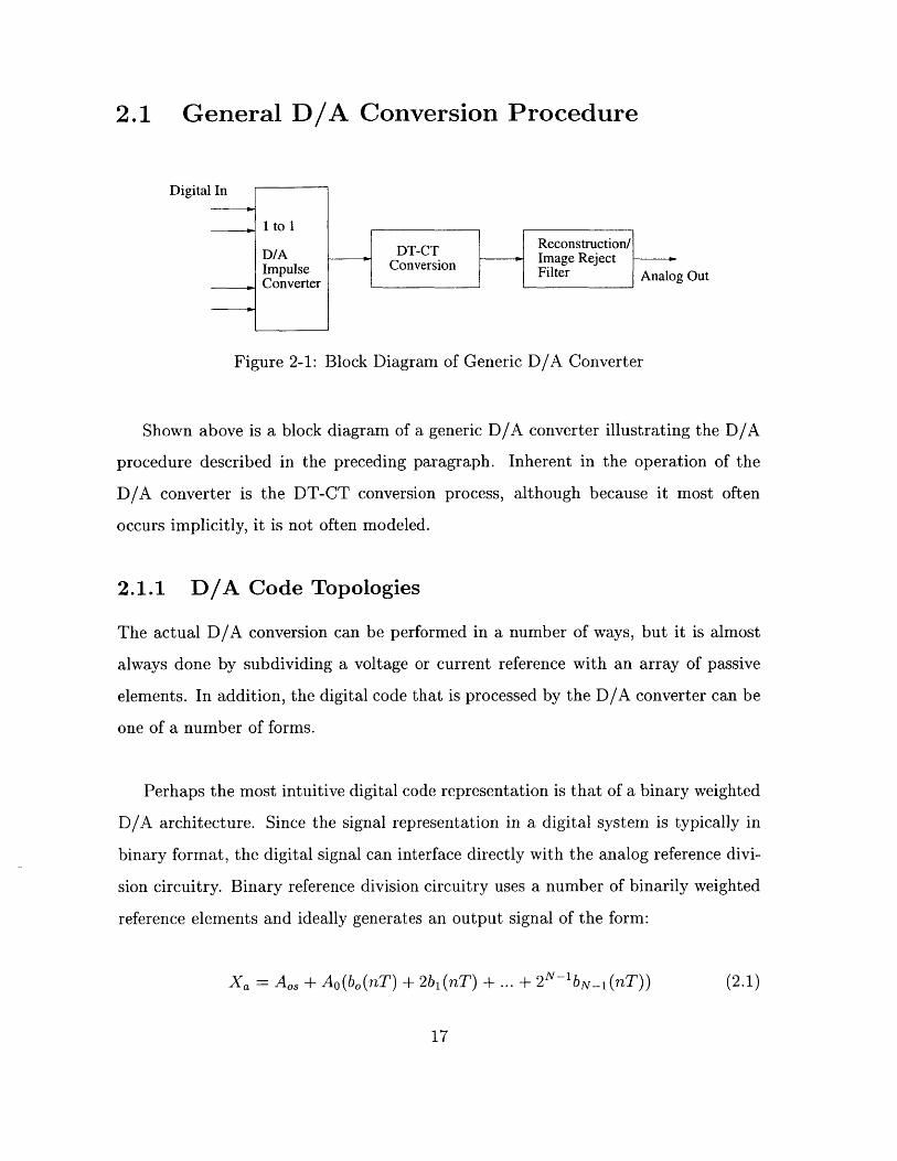
2.1 General D/A Conversion Procedure
Digital In
,I to I
D/A DT-CT Reconstruction/
Im ulseConversion - Image Reject -pe Filter Analog Out
.------ Converter
Figure 2-1: Block Diagram of Generic D/A Converter
Shown above is a block diagram of a generic D/A converter illustrating the D/A
procedure described in the preceding paragraph. Inherent in the operation of the
D/A converter is the DT-CT conversion process, although because it most often
occurs implicitly, it is not often modeled.
2.1.1 D/A Code Topologies
The actual D/A conversion can be performed in a number of ways, but it is almost
always done by subdividing a voltage or current reference with an array of passive
elements. In addition, the digital code that is processed by the D/A converter can be
one of a number of forms.
Perhaps the most intuitive digital code representation is that of a binary weighted
D/A architecture. Since the signal representation in a digital system is typically in
binary format, the digital signal can interface directly with the analog reference divi-
sion circuitry. Binary reference division circuitry uses a number of binarily weighted
reference elements and ideally generates an output signal of the form:
Xa = A,, + A0(b,(nT) + 2b 1(nT) + ... + 2N- 1 bN- 1 (nT)) (2.1)
17
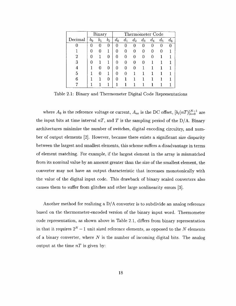
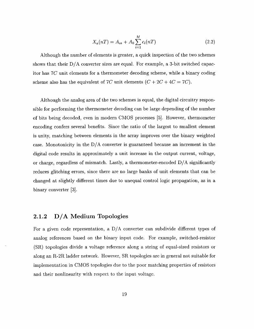
Binary Thermometer CodeDecimal bo b1 b2 do d1 d 2 d3 d4 d5 d 6
0 0 0 0 0 0 0 0 0 0 01 0 0 1 0 0 0 0 0 0 12 0 1 0 0 0 0 0 0 1 13 0 1 1 0 0 0 0 1 1 14 1 0 0 0 0 0 1 1 1 15 1 0 1 0 0 1 1 1 1 16 1 1 0 0 1 1 1 1 1 17 1 1 111 11 11 1
Table 2.1: Binary and Thermometer Digital Code Representations
where AO is the reference voltage or current, A,, is the DC offset, [b (nT)]'-' are
the input bits at time interval nT, and T is the sampling period of the D/A. Binary
architectures minimize the number of switches, digital encoding circuitry, and num-
ber of output elements [2]. However, because there exists a significant size disparity
between the largest and smallest elements, this scheme suffers a disadvantage in terms
of element matching. For example, if the largest element in the array is mismatched
from its nominal value by an amount greater than the size of the smallest element, the
converter may not have an output characteristic that increases monotonically with
the value of the digital input code. This drawback of binary scaled converters also
causes them to suffer from glitches and other large nonlinearity errors [3].
Another method for realizing a D/A converter is to subdivide an analog reference
based on the thermometer-encoded version of the binary input word. Thermometer
code representation, as shown above in Table 2.1, differs from binary representation
in that it requires 2N - 1 unit sized reference elements, as opposed to the N elements
of a binary converter, where N is the number of incoming digital bits. The analog
output at the time nT is given by:
18
M
Xa(nT) = A,, + AO Z ci(nT) (2.2)
Although the number of elements is greater, a quick inspection of the two schemes
shows that their D/A converter sizes are equal. For example, a 3-bit switched capac-
itor has 7C unit elements for a thermometer decoding scheme, while a binary coding
scheme also has the equivalent of 7C unit elements (C + 2C + 4C = 7C).
Although the analog area of the two schemes is equal, the digital circuitry respon-
sible for performing the thermometer decoding can be large depending of the number
of bits being decoded, even in modern CMOS processes [5]. However, thermometer
encoding confers several benefits. Since the ratio of the largest to smallest element
is unity, matching between elements in the array improves over the binary weighted
case. Monotonicity in the D/A converter is guaranteed because an increment in the
digital code results in approximately a unit increase in the output current, voltage,
or charge, regardless of mismatch. Lastly, a thermometer-encoded D/A significantly
reduces glitching errors, since there are no large banks of unit elements that can be
changed at slightly different times due to unequal control logic propagation, as in a
binary converter [3].
2.1.2 D/A Medium Topologies
For a given code representation, a D/A converter can subdivide different types of
analog references based on the binary input code. For example, switched-resistor
(SR) topologies divide a voltage reference along a string of equal-sized resistors or
along an R-2R ladder network. However, SR topologies are in general not suitable for
implementation in CMOS topologies due to the poor matching properties of resistors
and their nonlinearity with respect to the input voltage.
19
Switched-current (SI) topologies are quite suitable for implementation in CMOS
topologies, as current source arrays that are relatively insensitive to mismatch are easy
to design therein. In addition, the reference and summing elements (current source
references and I-V opamps) can be implemented in a robust manner. SI topologies
can be designed to operate at high frequencies and are often used in large-bandwidth
applications where very high speed in the D/A converter is required [2] [5]. Typically,
this class of D/A converter operates as a bank of thermometer or mixed (binary and
thermometer) encoded elements that are switched to the output summing node via
CMOS switches.
Switched-capacitor (SC) topologies subdivide an analog voltage reference by op-
erating on a two-phase system. On the first phase, the bits of the binary input word
determine which capacitors of the capacitor array will be charged to the reference
voltage Vef and which will be charged to ground such that the total charge on the
capacitors is proportional to the digital input word. On the second phase of operation,
the charges on the capacitors are combined, usually by discharging them to an opamp
virtual ground, where the total charge is integrated onto the opamp feedback capaci-
tor. Although the speed of the SC D/A is limited by the achievable opamp bandwidth
and the on resistance of the switches, it can present an attractive design option in that
the D/A converter will integrate nicely into an analog switched-capacitor postfilter.
2.1.3 Discrete Time - Continuous Time Interface
The most common DT-CT interface that is realized in D/A converters is a zero-order
hold. Zero-order hold (ZOH) operation occurs implicitly when the output of the D/A
converter is maintained at a constant level between sampling intervals. Although
ZOH operation is easily overlooked, it results in several nonidealities that affect the
20
operation of the overall D/A converter. For example, the continuous time frequency
response of the ZOH operation can be shown to be:
sin('f ) -iHo(f) =is e fs (2.3)
(7rf)/fs
For sampling frequencies near the Nyquist rate, the rolloff of this transfer function
severely attenuates in-band signal frequencies and must be compensated for in the
analog postfiltering scheme, posing an additional burden.
In addition, sampling time noise, commonly known as clock jitter, introduces dis-
tortion directly into the signal path by causing slight time displacements at the output
samples [6]. Although jitter-induced distortion is not technically noise, its effects are
often modeled as such, contributing to the overall signal-band noise performance of
the D/A converter [7].
2.1.4 Analog Postfiltering
The analog postfilter in the generic D/A converter compensates for the droop in the
zero-order-hold transfer function and rejects any out-of-band spectral images. Ideally,
the transfer function of this postfilter should be the inverse of the zero-order-hold
transfer function within the signal band and zero elsewhere [4]:
Hr(f) = e , f I < 2 (2.4)
Hr(f) = 0,|f > 2 (2.5)2
Of course, a filter with such a sharp cutoff is difficult to obtain in practice, a
limitation inherent in the design of Nyquist converters.
21
2.2 Nyquist Converters
Contrary to its namesake, a Nyquist D/A converter does not actually operate at the
Nyquist rate, but typically at a rate 1.5 to 10 times greater than required by the
Nyquist criterion in order to ease postfiltering requirements. The key characteristic
of a Nyquist converter, however, is that it generates a series of output analog values in
which each analog value has a one-to-one correspondence with a single digital input
value. The advantage of this setup is that the D/A conversion process is intuitive and
that the converter has a low speed of operation, reducing bandwidth requirements on
active devices that act as charge or current summers, as in the SC and SI topologies.
While Nyquist-rate converters can be implemented in an SR, SI, or SC topology,
they all generally require that the one-to-one digital-to-analog conversion be per-
formed to the overall precision of the converter. Since these one-to-one converters
almost invariably use matched elements to subdivide a reference voltage or current,
the overall precision of the converter is determined by the quality of the matching
in the available CMOS process. In general, this is no greater than 8-12 bits [8], but
can be improved through laser trimming of elements or error-correcting circuitry, the
first of which incurs a direct dollar cost, and the second of which can be expensive in
terms of power, area, and design time.
It was stated earlier that a Nyquist converter is typically operated at a sampling
rate 1.5 to 10 times greater than the Nyquist rate. To gain some appreciation as to
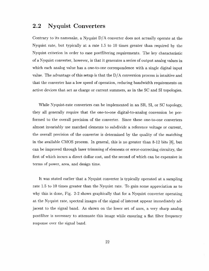
why this is done, Fig. 2-2 shows graphically that for a Nyquist converter operating
at the Nyquist rate, spectral images of the signal of interest appear immediately ad-
jacent to the signal band. As shown on the lower set of axes, a very sharp analog
postfilter is necessary to attenuate this image while ensuring a flat filter frequency
response over the signal band.
22
IP(x)I Baseband SpectralSignal ,,Images
fs12 fs 2fs 3fs 4fs f
IH(x)I A Frequency Response of Zero Order Hold
fs/2 fs 2fs 3fs 4fs f
Required Postfilter Rolloff Characteristic
|Y(x) I ZOH-Attenuated Baseband Signal
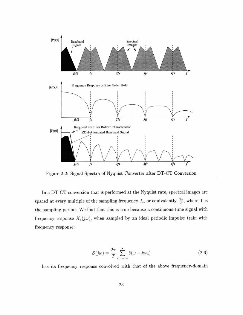
fs12 fs 2fs 3fs 4fs f
Figure 2-2: Signal Spectra of Nyquist Converter after DT-CT Conversion
In a DT-CT conversion that is performed at the Nyquist rate, spectral images are
spaced at every multiple of the sampling frequency fs, or equivalently, Lr, where T is
the sampling period. We find that this is true because a continuous-time signal with
frequency response Xc(jw), when sampled by an ideal periodic impulse train with
frequency response:
27SUWo) = T 6(w - kw,) (2.6)
k=-oo
has its frequency response convolved with that of the above frequency-domain
23

impulse train, resulting in a sampled signal with frequency response:
1XS(jW) = -X(jw) * S(jw) (2.7)
27r
where the convolution operation results in:
Xs(Jw) = Xc(j(w - kw,)) (2.8)Tk=-oo
We note that, if the bandwidth of signal is denoted as WN, the spectral images of
baseband signal do not overlap if the sampling frequency ws is greater than twice the
bandlimited frequency WN-
Ws - WN > WN, ws > 2 WN (2.9)
If Ws is even greater, these spectral images are spaced even farther apart. When
this is the case, the requirements on the rolloff of the analog reconstruction filter are
relaxed, as the attenuation of a lowpass filter increases at higher frequencies. In gen-
eral, a 40-60 dB attenuation of the spectral images is considered sufficient in digital
audio applications [9].
2.3 Oversampling D/A Converters
While Nyquist converters are suitable for applications in which the signal bandwidth
to be processed is on the same order of magnitude as the achievable clocking fre-
quency, contemporary CMOS processes are capable of operating at clock frequencies
much greater than many classes of analog signal, digital audio in particular. This
affords the analog designer the attractive design option to clock the D/A converter
much faster than the Nyquist rate, placing much of the filtering and element matching
24
burdens in the digital domain [3]. Oversampling converters commonly employ digital
noise shaping, also known as sigma-delta modulation, in order to reduce the number
of quantization bits at the D/A interface while shifting the majority of the additional
quantization noise out of the signal band. Reducing the number of D/A elements can
greatly ease the matching requirements for the D/A converter.
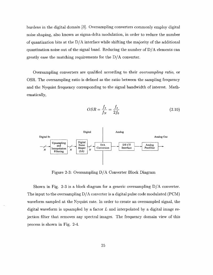
Oversampling converters are qualified according to their oversampling ratio, or
OSR. The oversampling ratio is defined as the ratio between the sampling frequency
and the Nyquist frequency corresponding to the signal bandwidth of interest. Math-
ematically,
OSR - S - S (2.10)fN 2fo
Digital Analog
Digital In Analog Out
Upsampling Digitaland Noise D/A DT-CT Analog
Interpolation N Shaper N Conversion Interface PostfilterN Filtering N (1A)NI
Figure 2-3: Oversampling D/A Converter Block Diagram
Shown in Fig. 2-3 is a block diagram for a generic oversampling D/A converter.
The input to the oversampling D/A converter is a digital pulse code modulated (PCM)
waveform sampled at the Nyquist rate. In order to create an oversampled signal, the
digital waveform is upsampled by a factor L and interpolated by a digital image re-
jection filter that removes any spectral images. The frequency domain view of this
process is shown in Fig. 2-4.
25
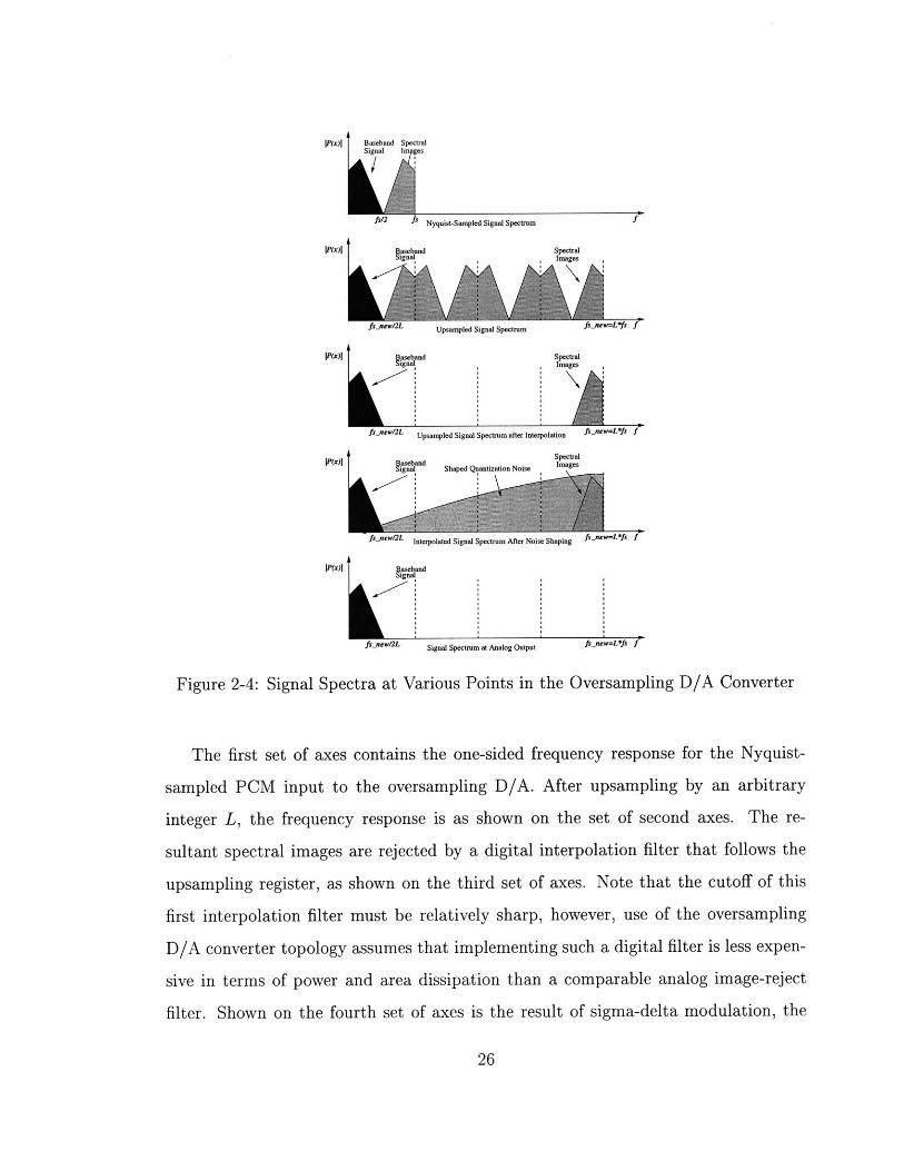
P(x)I Baseband Spectral
fs/2 s Nyquist-Sampled Signal Spectrum
PxI Baseand SpectralSignal, Images
fs new/2L Upsampled Signal Spectrum fs_new=Lfs f
IPWXI Baseband Setasignal Iae
fs-new/2L Upsampled Signal Spectrum after Interpolation fs-ne=LIs f
IP~x~ BaseasalSpectralignal Shaped Qtantization Noise
fsnew/2L Interpolated Signal Spectrum After Noise Shaping fs_e-=L*fs f
fs-new/2L Signal Spectrum at Analog Output fi-,ew=L*fs f
Figure 2-4: Signal Spectra at Various Points in the Oversampling D/A Converter
The first set of axes contains the one-sided frequency response for the Nyquist-
sampled PCM input to the oversampling D/A. After upsampling by an arbitrary
integer L, the frequency response is as shown on the set of second axes. The re-
sultant spectral images are rejected by a digital interpolation filter that follows the
upsampling register, as shown on the third set of axes. Note that the cutoff of this
first interpolation filter must be relatively sharp, however, use of the oversampling
D/A converter topology assumes that implementing such a digital filter is less expen-
sive in terms of power and area dissipation than a comparable analog image-reject
filter. Shown on the fourth set of axes is the result of sigma-delta modulation, the
26
addition of out-of-band shaped quantization noise to the signal, and on the fifth set
of axes is the signal spectrum at the output of the analog postfilter.
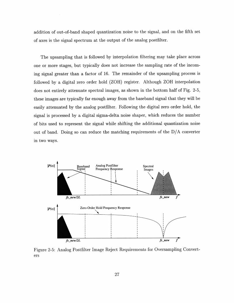
The upsampling that is followed by interpolation filtering may take place across
one or more stages, but typically does not increase the sampling rate of the incom-
ing signal greater than a factor of 16. The remainder of the upsampling process is
followed by a digital zero order hold (ZOH) register. Although ZOH interpolation
does not entirely attenuate spectral images, as shown in the bottom half of Fig. 2-5,
these images are typically far enough away from the baseband signal that they will be
easily attenuated by the analog postfilter. Following the digital zero order hold, the
signal is processed by a digital sigma-delta noise shaper, which reduces the number
of bits used to represent the signal while shifting the additional quantization noise
out of band. Doing so can reduce the matching requirements of the D/A converter
in two ways.
IP(X)I Baseband Analog Postfilter SpectralSignal Frequency Repne ,Images
fs-new/2L fsjnew f
IPWx)I Zero-Order Hold Frequency Response
fsjnewl2L fs-new f
Figure 2-5: Analog Postfilter Image Reject Requirements for Oversampling Convert-ers
27
The first of these is to reduce the number of quantizer bits at the sigma-delta
output to one, thus reducing the D/A converter to a two level output. Provided that
the two levels of the D/A converter are time invariant, the D/A converter is precisely
linear, containing only a gain error. Although linearity is guaranteed in this scheme,
quantizing the digital signal down to 1 bit introduces a large amount of quantization
noise, some of which may remain in the signal band if the oversampling ratio is not
large.
The second method of reducing the element matching burden is to use a multibit
D/A converter with a small (3-6) number of output bits. This reduces quantization
noise over the entire frequency range from the 1-bit case, but still keeps the number
of output elements relatively low such that D/A array linearization schemes become
feasible. To alleviate mismatch problems, the D/A converter elements are either cali-
brated [5] or swapped in a general class of pseudo random switching techniques known
as dynamic element matching (DEM) [12]. Although these techniques can make the
effects of element mismatch negligible, they become exponentially more costly to im-
plement as the number of sigma-delta output bits increases linearly.
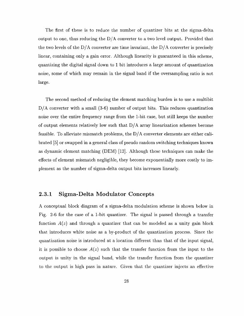
2.3.1 Sigma-Delta Modulator Concepts
A conceptual block diagram of a sigma-delta modulation scheme is shown below in
Fig. 2-6 for the case of a 1-bit quantizer. The signal is passed through a transfer
function A(z) and through a quantizer that can be modeled as a unity gain block
that introduces white noise as a by-product of the quantization process. Since the
quantization noise is introduced at a location different than that of the input signal,
it is possible to choose A(z) such that the transfer function from the input to the
output is unity in the signal band, while the transfer function from the quantizer
to the output is high pass in nature. Given that the quantizer injects an effective
28
noise signal e(n) into the modulator and that a signal x(n) enters the modulator at its
input, we can derive a signal transfer function S(z) and a noise transfer function N(z).
Y(z) _A(z)
S(Z ( A(z) (2.11)X(z) A(z)b1 + 1
Y(z) _ 1N(z) E(z) - 1 (2.12)
E(z) A(z)b + 1
we also have by superposition
Y(z) = S(z)X(z) + N(z)E(z) (2.13)
Quantizer (1-bit)
x(n) w(n) -- y(n)A(z)
Figure 2-6: Sigma-Delta Modulator Concept
We thus would like to choose A(z) such that it is large in the signal band If I < fo
such that S(z) approximates unity within this range and that N(z) approximates
zero in the same region, maximizing the inband signal-to-noise ratio. One such trans-
fer function that is easily implemented in digital circuitry is that of a discrete-time
integrator, specifically:
z- 1
A(z) 1 (2.14)Nn+ z-1
Note that the transfer function has a pole at dc (z=1) and decreases in magnitude
29
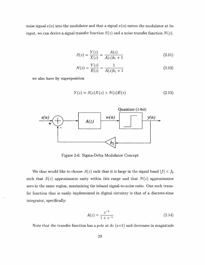
as z moves across the unit circle to z=-1. This implementation is shown in Fig. 2-7.
e(n)
x(n) ++wn
+4
y(n)
Figure 2-7: Sigma-Delta Modulator Block Diagram
Substituting in for A(z) and setting b1 to unity to simplify the analysis, we obtain
the transfer functions for this sigma-delta modulator.
S(z) = = (X(z)
Y(z)E(z)
Z- 1
1+z-_ = z -1z- 1
1+z'l+1
1_1 (1 - z 1 )
1+z-l+1
We see that the transfer function from the signal input to the output is merely a
delay, while the transfer function from the quantizer to the output is a discrete-time
differentiation, which is high-pass in nature. In the frequency domain, the transfer
function seen at the quantizer input is:
£~rL 2i~L-_ rf_ e fs - e C fs -( 1
N(f) = 1 - e fs - 2. 2j -e T, (2.17)
Taking the magnitude of both sides, we obtain:
IN(f)j = 2 sin (*) (2.18)
Equation 2.18 represents a high-pass transfer function. It follows that since the
30
(2.15)
(2.16)
C
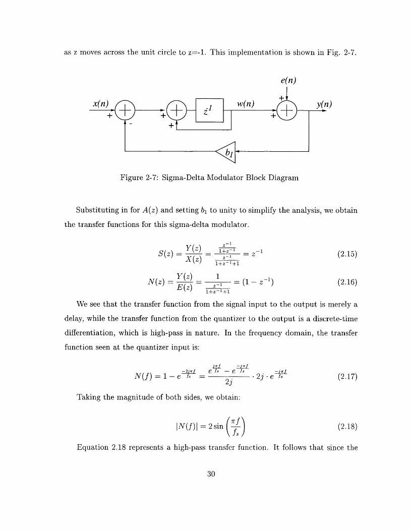
transfer function from the quantizer to the output is high-pass in nature, the larger
the oversampling ratio is made, the more confined the signal bandwidth fo will be
to the frequencies where the magnitude of the noise transfer function is very low.
This concept, illustrated below in Fig. 2-8 introduces one of the key design tradeoffs
inherent in low power, low area D/A converter design. Although increasing the OSR
decreases the amount of in-band quantization noise, the increased operating speed
imposes an additional burden on the analog postfilter, the burden depending on the
type of D/A converter and postfilter used.
IP(OI iSignal BandwidthShaped Quantization Noise
Figure 2-8: Oversampling Advantage
2.3.2 Analog Postfilter
Although the sigma-delta modulator ensures that most of the noise introduced by its
quantizer lies outside of the signal band, it is often to great advantage to filter out
this noise regardless of its effect (or lack thereof) on the signal. For example, un-
filtered D/A converter quantization noise could corrupt intermediate frequency (IF)
signal processing in adjacent RF circuitry. In addition, this noise could mix with
a high-frequency clock signal, resulting in intermodulation products that are mixed
down to baseband before reaching the output of the analog chip. Finally, in the case
31
of a discrete-time postfilter (some postfilters can be discrete-time and analog), the
reduction of out-of-band quantization noise improves the jitter performance of the
D/A converter [17] [40]. Therefore, a general rule of thumb is that the analog post-
filter for an oversampling converter must be of the same order or higher than that of
the sigma delta modulator. This ensures that the sigma-delta quantization noise as
a function of frequency does not rise faster than the increase in postfilter attenuation
as a function of frequency.
For typical values of oversampling ratios, which range from 64 to 512, the effect
of the zero order hold droop arising from the DT-CT conversion is negligible across
the signal band, as shown in Fig. 2-5. Thus, the analog postfilter does not need to
compensate for ZOH droop, as is required in the Nyquist converter. In addition, the
only spectral images that need to be suppressed by the analog postfilter occur at Kf0
where K is the total amount of upsampling that is followed by digital interpolation
filtering. However, it is typical that attenuating the out of band sigma-delta quanti-
zation noise is the more stringent requirement on the postfilter, as K is usually close
to an order of magnitude greater than unity.
Analog postfilters are either implemented in active-RC fashion or as a switched-
capacitor topology. The former are preferred in current-mode converters, as an active-
RC filter can also double as an I-V converter provided that the input resistor is re-
moved. Switched-capacitor postfilters are convenient to implement when the D/A
converter is already a switched-capacitor topology.
32
2.4 D/A Converter Metrics
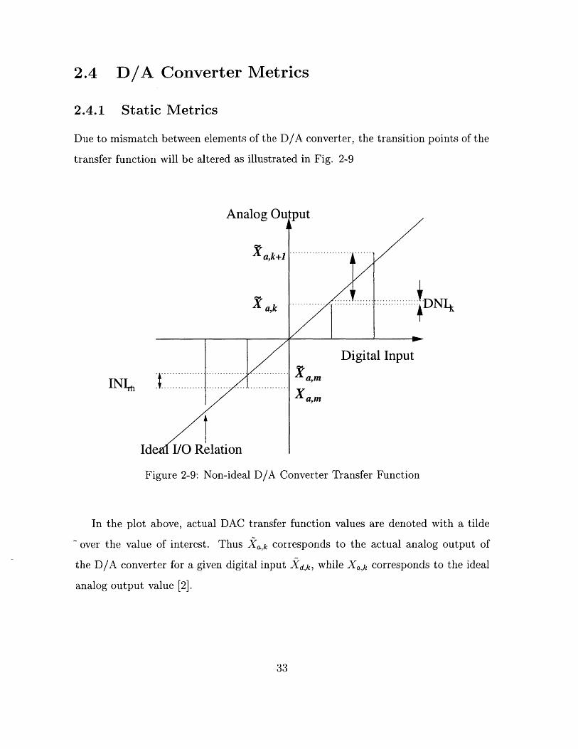
2.4.1 Static Metrics
Due to mismatch between elements of the D/A converter, the transition points of the
transfer function will be altered as illustrated in Fig. 2-9
Analog Output
Xa,k+1
a,k
I............. . ........ ......I ..... .......
IdLI/O LRelation
Digital InputX a,m
Xa,m
Figure 2-9: Non-ideal D/A Converter Transfer Function
In the plot above, actual DAC transfer function values are denoted with a tilde
over the value of interest. Thus Xa,k corresponds to the actual analog output of
the D/A converter for a given digital input Xd,k, while Xa,k corresponds to the ideal
analog output value [2].
33
DNI4
INI11
F
............. ......
........... .......'x ........
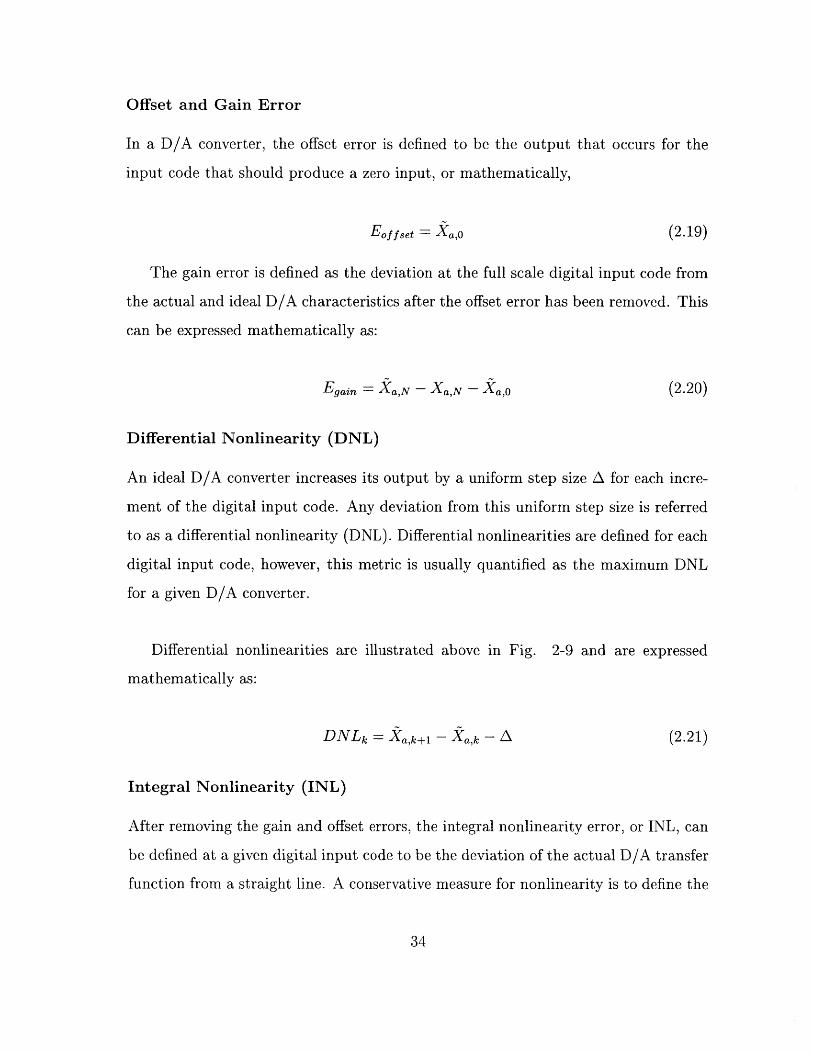
Offset and Gain Error
In a D/A converter, the offset error is defined to be the output that occurs for the
input code that should produce a zero input, or mathematically,
Eoffset = Xa, 0 (2.19)
The gain error is defined as the deviation at the full scale digital input code from
the actual and ideal D/A characteristics after the offset error has been removed. This
can be expressed mathematically as:
Egain X a,N - Xa,N - Xa,O (2.20)
Differential Nonlinearity (DNL)
An ideal D/A converter increases its output by a uniform step size A for each incre-
ment of the digital input code. Any deviation from this uniform step size is referred
to as a differential nonlinearity (DNL). Differential nonlinearities are defined for each
digital input code, however, this metric is usually quantified as the maximum DNL
for a given D/A converter.
Differential nonlinearities are illustrated above in Fig. 2-9 and are expressed
mathematically as:
DNLk = Xa,k+1 - Xa,k - A (2.21)
Integral Nonlinearity (INL)
After removing the gain and offset errors, the integral nonlinearity error, or INL, can
be defined at a given digital input code to be the deviation of the actual D/A transfer
function from a straight line. A conservative measure for nonlinearity is to define the
34
straight line to be the line connecting the analog output values Xa,N, Xa,O. Another
measure chooses the straight line to be the linear best-fit to the actual D/A transfer
function. The relationship between INL and DNL is given by:
k
INLk = ( DNLI (2.22)1-i
Monotonicity
A monotonic D/A converter is one in which the analog output level always increases
with an increment in the digital input code. In order words, the slope of the digi-
tal/analog characteristic is always positive or negative, but never both.
2.4.2 Frequency Domain Metrics
Although static D/A converter metrics are useful in quantifying the performance of
Nyquist-rate converters, most contemporary oversampling converters are quantified
using frequency domain metrics. This is because most oversampling converters em-
ploy calibration, DEM, or a two-level D/A to either significantly reduce or to eliminate
D/A nonlinearities altogether.
Since the dominant nonidealities of the oversampling converter are typically the
remaining in-band quantization noise, analog postfilter component noise, and analog
postfilter harmonic distortion, more useful metrics of performance include signal-to-
noise ratio (SNR) and total harmonic distortion. This performance is often deter-
mined by using a single-tone input sinusoid, but two-tone and multi-tone tests may
yield more useful information if intermodulation distortion is considered relevant to
the converter's operation.
35
Signal to Noise Ratio
Typically, the noise in an oversampling D/A converter is determined by applying a
sinusoidal signal at the input, then integrating the resultant output noise across the
signal bandwidth. For audio D/A converters, this integration is often performed tak-
ing the characteristics of the human ear into account, a process known as A-weighting.
The ratio between the rms power of the output sinusoid to this integrated noise power
is thus the signal to noise ratio, and is usually expressed in terms of decibels. In this
project, the SNR will be measured by integrating the unweighted noise from 20Hz to
20000kHz as an approximation to the A-weighting method.
SNR = 10 logo S Power (2.23)Integrated Noise Power
Total Harmonic Distortion
The total harmonic distortion (THD) is the ratio of the rms sum of the powers of the
single-tone harmonics to the power of the input fundamental tone.
THD _ 1 logo ( Sum of Harmonic Powers (.4Signal (Fundamental Tone) Power
THD = 10 logo ( (2.25)(k=2 I
where X 1 is the voltage level of the fundamental tone and Xk the rms voltage of
the kth harmonic component.
Other Measures
In addition to these two measurements, combinations or qualifications thereof are also
common metrics in oversampling D/A design.
36
Signal-to-quantization noise ratio, or SQNR, is computed the same as the signal-
to-noise ratio, except only digital quantization noise is included in the computation.
Signal-to-noise-and-distortion ratio (SNDR) is computed as the ratio between the
signal power and the sums of the integrated noise and the total distortion power over
a given signal bandwidth.
Dynamic range is defined as the ratio between the largest signal output magnitude
available from the D/A converter to the smallest signal that is resolvable above the
noise floor.
2.5 Oversampling D/A Optimization Strategies
Even without a priori knowledge of the performance of the individual blocks of the
oversampling D/A converter, a general strategy for optimizing the output-referred
SNR from a system level perspective can be described.
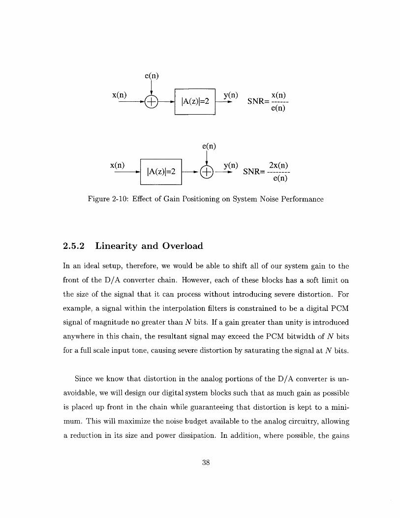
2.5.1 Gain and Noise
As the signal passes through each of the blocks described above, some amount of noise
is added to the signal, whether it be from digital truncation effects or thermal noise
from analog components. It can be seen quite readily that it is not optimal to place a
large gain after a dominant noise source, as this results in subsequent amplification of
the noise. Rather, if the gain, or part of it, can be placed before the dominant noise
source, the overall performance of the system will improve, as the signal is amplified
before the noise is added to it.
37
e(n)
x(n) y(n) x(n)IA(z)I=2 e--) SNR-
e(n)
x(n) y(n) 2x(n)jA(z)j=2 - SNR= ------
e(n)
Figure 2-10: Effect of Gain Positioning on System Noise Performance
2.5.2 Linearity and Overload
In an ideal setup, therefore, we would be able to shift all of our system gain to the
front of the D/A converter chain. However, each of these blocks has a soft limit on
the size of the signal that it can process without introducing severe distortion. For
example, a signal within the interpolation filters is constrained to be a digital PCM
signal of magnitude no greater than N bits. If a gain greater than unity is introduced
anywhere in this chain, the resultant signal may exceed the PCM bitwidth of N bits
for a full scale input tone, causing severe distortion by saturating the signal at N bits.
Since we know that distortion in the analog portions of the D/A converter is un-
avoidable, we will design our digital system blocks such that as much gain as possible
is placed up front in the chain while guaranteeing that distortion is kept to a mini-
mum. This will maximize the noise budget available to the analog circuitry, allowing
a reduction in its size and power dissipation. In addition, where possible, the gains
38

present in the analog blocks will be minimized to the extent that the signal does not
incur significant distortion within the analog circuitry.
39
Chapter 3
Digital Interpolation and Noise
Shaping
Unlike analog circuitry, whose accuracy is limited by physical factors such as ther-
mal noise and finite supply voltage, digital circuitry can be made arbitrarily precise,
assuming that an infinite number of bits are available to represent a digital signal.
Advances in process technology over the last twenty years have scaled down the di-
mensions of digital circuitry, enabling the implementation of large bit width signal
paths without incurring a severe cost in terms of circuit speed and die area [10]. In
order to achieve low power and area consumption in the analog portion of the D/A
converter, it is thus desirable to shift as much of the noise burden to the digital por-
tion as possible, inasmuch as it can be easily absorbed.
Furthermore, in many industry applications, part of the digital D/A converter
circuitry is implemented in a digital signal processing (DSP) core where specialized
digital architectures optimized for polyphase filtering handle a number of signal pro-
cessing operations. Although the digital filtering requirements of the D/A are likely
to only form a small fraction of the filtering load performed by the DSP, the bus
bit widths available to the outputs of the digital interpolation filters are usually de-
40
termined by system architecture considerations rather than D/A converter digital
accuracy requirements, resulting in an upper bound on the SNR available from the
digital portion of the converter.
3.1 Digital Quantization Noise
Because the quantization process is highly nonlinear, its exact analysis, although
necessary to precisely predict the performance of the D/A converter, is particularly
troublesome. When quantization is incorporated into a multiple feedback loop, as
in a sigma-delta modulator, the analysis becomes even more difficult. In order to
make this analysis tractable, various methods based on certain assumptions and ap-
proximations have been introduced and applied with successful results [14]. Even
in very practical circumstances where the simplifying assumptions regarding quanti-
zation have been completely violated, useful results can still be obtained, especially
given that a more precise analysis is either prohibitively difficult or impossible.
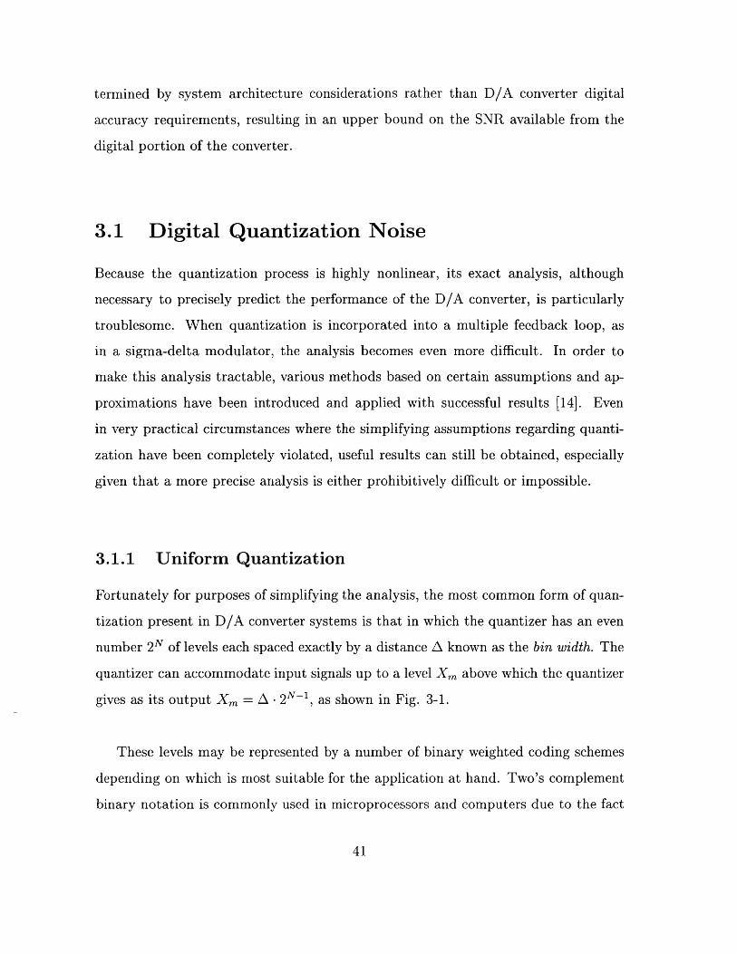
3.1.1 Uniform Quantization
Fortunately for purposes of simplifying the analysis, the most common form of quan-
tization present in D/A converter systems is that in which the quantizer has an even
number 2 N of levels each spaced exactly by a distance A known as the bin width. The
quantizer can accommodate input signals up to a level Xm above which the quantizer
gives as its output Xm = A - 2 N-1, as shown in Fig. 3-1.
These levels may be represented by a number of binary weighted coding schemes
depending on which is most suitable for the application at hand. Two's complement
binary notation is commonly used in microprocessors and computers due to the fact
41
3A
2A
A
-X,, -3A -2A -A
\ K NKN
Quantizer Out
Quantizer In
A 2A 3A Xm-A
-2A
-3A
Quantizer Error
K N N Quantizer InI N N\A
Figure 3-1: Input/Output Relation and Input/Error Relation for a Uniform Quantizer
that addition of positive and negative numbers can be performed by straightforward
addition without the use of specialized arithmetic blocks. Also, the subtraction of
two numbers is easily performed by complementing the bits of the number to be
subtracted, adding one LSB to create the two's complement of the number to be
subtracted, then finally adding the first of the two numbers in the subtraction op-
eration [3]. For the same reason, this representation is also commonly used in DSP
processors. As shown in Table 3.1, in the two's complement notation, the leftmost bit
is taken as the sign bit, where "0" denotes a positive integer, while a "1" denotes a
negative integer. The remaining binary digits denote the specific number or fraction
42
N N N \
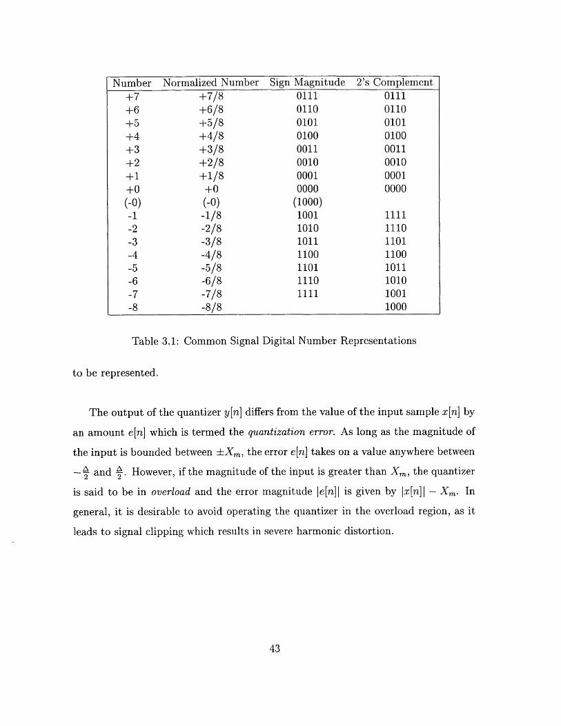
Number Normalized Number Sign Magnitude 2's Complement+7 +7/8 0111 0111+6 +6/8 0110 0110+5 +5/8 0101 0101+4 +4/8 0100 0100+3 +3/8 0011 0011+2 +2/8 0010 0010+1 +1/8 0001 0001+0 +0 0000 0000
(-0) (-0) (1000)-1 -1/8 1001 1111-2 -2/8 1010 1110-3 -3/8 1011 1101-4 -4/8 1100 1100-5 -5/8 1101 1011-6 -6/8 1110 1010-7 -7/8 1111 1001-8 -8/8 1000
Table 3.1: Common Signal Digital Number Representations
to be represented.
The output of the quantizer y[n] differs from the value of the input sample x[n] by
an amount e[n] which is termed the quantization error. As long as the magnitude of
the input is bounded between ±Xm, the error e[n] takes on a value anywhere between
- and . However, if the magnitude of the input is greater than Xm, the quantizer
is said to be in overload and the error magnitude Ie[n]I is given by jx[n] - Xm. In
general, it is desirable to avoid operating the quantizer in the overload region, as it
leads to signal clipping which results in severe harmonic distortion.
43
3.1.2 Quantization Noise Linearization Approximation
Although a uniform quantizer inherently introduces signal-dependent nonlinear errors
into the signal path, the classic study conducted by Bennett [11] developed a set of
conditions by which the quantization operation can be approximated by an additive
white noise source.
Bennett's theorem postulates that if the following conditions are met:
I. That the quantizer input is not in the overload region.
II. That the number of levels in the quantizer is asymptotically large.
III. That the spacing A between quantizer levels is asymptotically small.
IV. That the joint probability density function (pdf) of the input signal is
smooth at different sample times.
Then the quantization error sequence e[n] has the following properties:
Property 1. e[n] is statistically independent of the input signal u[n].
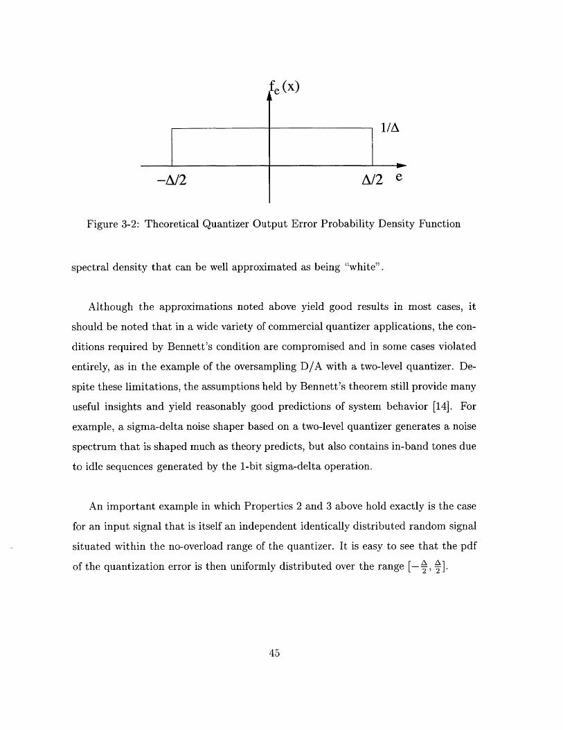
Property 2. The pdf of e[n] is uniformly distributed in [-, $]. It is an unbiased
estimator of the input signal, that is to say, E[y[n]] ~ E[x[n]], as shown
in Fig. 3-2.
Property 3. e[n] has a flat power spectral density (i.e. is "white").
The ability to replace a nonlinear quantizer with a linear noise source consider-
ably simplifies the analysis involved because the well-developed body of linear systems
theory can now be applied to digital blocks in a mixed-signal system. As shown in
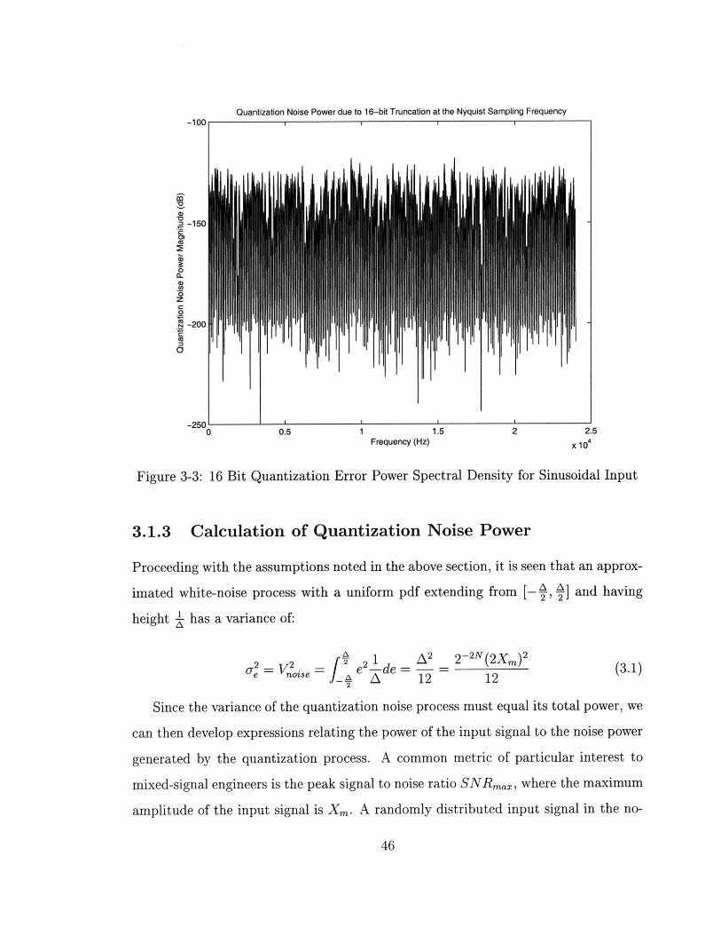
Fig. 3-3, quantization of a full scale sinusoid to 16 bits in MATLAB yields a power
44
~e(x
1/A
-A/2 A/2 e
Figure 3-2: Theoretical Quantizer Output Error Probability Density Function
spectral density that can be well approximated as being "white".
Although the approximations noted above yield good results in most cases, it
should be noted that in a wide variety of commercial quantizer applications, the con-
ditions required by Bennett's condition are compromised and in some cases violated
entirely, as in the example of the oversampling D/A with a two-level quantizer. De-
spite these limitations, the assumptions held by Bennett's theorem still provide many
useful insights and yield reasonably good predictions of system behavior [14]. For
example, a sigma-delta noise shaper based on a two-level quantizer generates a noise
spectrum that is shaped much as theory predicts, but also contains in-band tones due
to idle sequences generated by the 1-bit sigma-delta operation.
An important example in which Properties 2 and 3 above hold exactly is the case
for an input signal that is itself an independent identically distributed random signal
situated within the no-overload range of the quantizer. It is easy to see that the pdf
of the quantization error is then uniformly distributed over the range [-$, $].
45
Quantization Noise Power due to 16-bit Truncation at the Nyquist Sampling Frequency-100 1 1 - I
.- 150CCM
0a-
0
C0
.N-200
-2500
''lII
0.5Frequency (Hz)
1.5 2 2.5
x 104
Figure 3-3: 16 Bit Quantization Error Power Spectral Density for Sinusoidal Input
3.1.3 Calculation of Quantization Noise Power
Proceeding with the assumptions noted in the above section, it is seen that an approx-
imated white-noise process with a uniform pdf extending from [-A, 4] and having
height 1 has a variance of:
- 1 2 2-2N(2X )22 2 = e 2 de = 2 = _ 2_ m
or noise A z 12 12 (3.1)
Since the variance of the quantization noise process must equal its total power, we
can then develop expressions relating the power of the input signal to the noise power
generated by the quantization process. A common metric of particular interest to
mixed-signal engineers is the peak signal to noise ratio SNRma, where the maximum
amplitude of the input signal is Xm. A randomly distributed input signal in the no-
46
1
overload range thus has a signal power of:
V2gnai -(2Xm)2 (3.2)signal = 12
which gives an SNR of:
10 log1 o = 10 logio(2 2 N) = 6.02N dB (3.3)(VnOise)
A sinusoidal signal can be analyzed the same way. A full-scale sinusoidal signal
has a power of:
V2 X 2
signal =2 (3.4)
which gives a peak SNR of:
SNRmax = 10 log, 2" = 10 logo 2 2N = 6.02N + 1.76 dB (3.5)0 VOise (
Since a full-scale sinusoid results in the maximum SNR for a quantizer, we denote
this quantity as SNRmax.
3.1.4 Quantization Noise Power with Oversampling
Continuing to assume that the quantization process yields an error sequence e[n] that
can be modeled as white noise, for an oversampled system, the quantization error
power is spread uniformly across the frequency range [-, L J, where fs is a sampling
frequency much greater than the Nyquist rate. Since the resultant power spectral
density is equal to the variance of the error sequence e[n], the quantization noise
power per unit Hz frequency must be given by:
A2 1Se(f) = (3.6)
12 fs
47

In an oversampled D/A converter, the primary parameter of interest is not the
SNR per se, but the SNR across the signal bandwidth fo. Thus, to calculate the in-
band SNR, we first integrate the noise power spectral density across the signal band.
Remembering to integrate across both sides of the two-sided power spectral density,
we obtain:
2 A2 2fo A2 1e 12 fs 12 OSR
Again, assuming a sinusoidal input signal, which is commonly used to characterize
the noise performance of a D/A converter,
2 A2 2 2N (2Xm) 2
S - (3.8)8 8
Taking the logarithm ratio of the signal power to the error power yields:
SNRmax 10190 og 22N +l10o 10 1OSR =6.02N+1.76+0logiOOSR dB (3.9)
Thus, as the signal of interest is oversampled, the SNR increases by about 10dB
for every additional decade of oversampling. Equivalently, for each factor of four in-
crease in OSR, an additional bit of resolution is obtained. While this improvement
seems impressive, increasing the effective bit resolution through straight oversampling
quickly becomes expensive. For example, consider a 5-bit quantizer that we would
like to use to convert an oversampled signal with 16 bits of audio signal band resolu-
tion. This requires an oversampling ratio of 4,200,000, corresponding to a sampling
frequency of 201GHz, a rate not currently attainable with modern CMOS processes.
Fortunately, the use of sigma-delta modulation helps to achieve the desired signal
resolution without such a dramatic increase in sampling rate.
The reason for the improvement in SNR with the oversampling ratio is that more
48
samples are taken per unit time. Prior to the point where the system SNR is measured,
these samples are averaged out via low-pass filtering to reconstruct the baseband
signal. During this averaging, the baseband signal components add linearly because
they are self-correlated. However, the quasi-random quantization error has an impulse
autocorrelation function and thus adds as the square root of the sum of the squares
[3].
3.2 Digital Interpolation Filtering
3.2.1 Upsampling
The process by which the sampling frequency is increased in an oversampling converter
is colloquially referred to as interpolation but more accurately should be referred to as
upsampling followed by image-reject filtering. When a discrete-time signal is upsam-
pled by a factor L, each sample of the original signal is mapped to every Lth sample
in the new signal sequence, which runs at a sampling rate L times greater than that
of the original. The remainder of the samples retain a value of zero. Obviously, the
upsampling process produces some unwanted modification to the input signal. This
modification is best viewed in the frequency domain and is derived as follows:
The upsampling process can be expressed in the discrete time domain as:
X [in] x[n/L] if n = 0, ±L, ±2L, ... (3.10)0 otherwise
equivalently, we can express the above case statement as:
xU[n] = x[k]6[n - kL] (3.11)k=-oo
Given the discrete-time Fourier transform
49
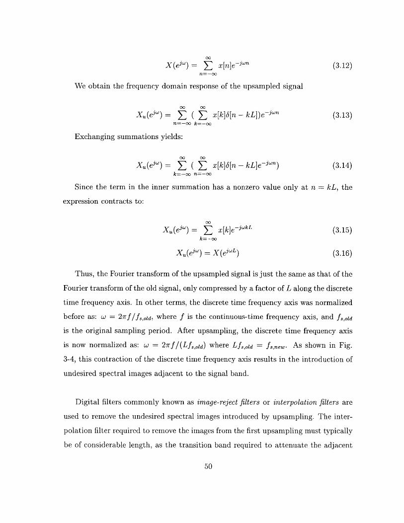
00
X(eiw) = E x[n]e-i" (3.12)n=-oo
We obtain the frequency domain response of the upsampled signal
Xu(eiw) = E ( E Z [k]6[n - kL])e-jon (3.13)n=-00 k=-oo
Exchanging summations yields:
Xu(eiw) = E ( E x[k]6[n - k Le-i") (3.14)k=-oo n=-oo
Since the term in the inner summation has a nonzero value only at n = kL, the
expression contracts to:
X )= S x[k]e-jwkL (3.15)k=-oo
Xu(e") - X(e L) (3.16)
Thus, the Fourier transform of the upsampled signal is just the same as that of the
Fourier transform of the old signal, only compressed by a factor of L along the discrete
time frequency axis. In other terms, the discrete time frequency axis was normalized
before as: w = 27f/fS,otd, where f is the continuous-time frequency axis, and fs,old
is the original sampling period. After upsampling, the discrete time frequency axis
is now normalized as: w = 27rf /(LfS,,Id) where Lf,Old = fs,new. As shown in Fig.
3-4, this contraction of the discrete time frequency axis results in the introduction of
undesired spectral images adjacent to the signal band.
Digital filters commonly known as image-reject filters or interpolation filters are
used to remove the undesired spectral images introduced by upsampling. The inter-
polation filter required to remove the images from the first upsampling must typically
be of considerable length, as the transition band required to attenuate the adjacent
50
00 0
IUpsamplingResults In
0000
x[n]Tf t o
xu[n]
Spectral ImageL Baseband Signal
IX(e') )L
0f
IXu(eW ) I Baseband Sig
fs/2 3fs/4 ,s
lna Spectral Images
0 fs/4 fs/2 3fs/4 fs
Figure 3-4: Discrete-Time and Frequency Domain Depictions of Upsampling
spectral image is very narrow. As a low-pass interpolation filter in effect performs
an averaging operation on the upsampled signal, the signal magnitude is reduced by
a factor of L for a filter with OdB gain. In order to maintain the filtered upsampled
signal at its original magnitude, the filter must have a gain of L associated with it.
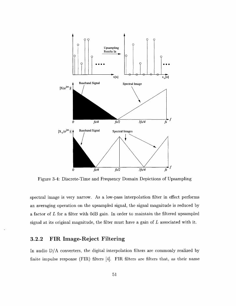
3.2.2 FIR Image-Reject Filtering
In audio D/A converters, the digital interpolation filters are commonly realized by
finite impulse response (FIR) filters [4]. FIR filters are filters that, as their name
51
If0
X\s/4
implies, have impulse responses that are bounded in time. In general, they are im-
plemented as shown in Fig. 3-5 as a bank of digital multipliers whose inputs are
separated by delay registers and whose outputs are summed to generate the filter
output.
DigitalFIR
Output
Figure 3-5: Digital Implementation of FIR Interpolation Filter
FIR filters are frequently used in audio applications because an FIR filter can be
easily designed to have linear phase, and thus constant group delay, which minimizes
phase distortion of the audio signal. To see how this can be accomplished, consider a
time-bounded filter of length M such that:
he[fl] = he[-n] (3.17)
Taking its discrete-time Fourier transform yields:
n=M/2 M/2
He (eiw) = E he[n]e-s'" = he[O] + Z 2he[lIcos(Wo) (3.18)n=-M/2 n=1
Since the filter is time-bounded and even, its discrete-time frequency response is
purely real and thus has zero phase. Of course, such a filter is not causal and is hence
impossible to implement. However, adding a time delay to the filter such as to make
it purely causal only has the effect of adding a linear phase to the frequency response:
52
h[n] he[n - M/2] (3.19)
H(ew) = He(ejw)ejwM/2 (3.20)
1H(ew)I = IHe(ejw)1 (3.21)
ZH(ejw) = -jwM/2 (3.22)
Contemporary design of optimal FIR filters is greatly aided by the use of filter
design software algorithms. One particularly effective and ubiquitous FIR design
algorithm was developed by Parks and McClellan[19] , which takes as its arguments
the desired filter passband edge wp, the desired filter stopband edge w, the number
of filter taps M, and the desired passband and stopband errors, denoted 61 and 62
respectively. The Parks and McClellan algorithm fixes wp, w, and M while letting 61
and 62 vary. The resulting optimal lowpass filter has an equiripple response in both
the passband and the stopband. Kaiser [20] performed a computational study of this
method and subsequently obtained a relation between the parameters of the filters,
with gives the number of taps as:
-10 log 1 (6162) - 13 (3.23)2.324Aw
where
AW = W, - WP (3.24)
for a lowpass filter.
Thus, for a given error specification in the passband and stopband, there exists
a tradeoff between the sharpness of the filter transition band and the number of the
taps in the filter. It is also evident that if a signal is interpolated by a large factor
L, the transition band of the interpolation filter must be incredibly sharp in order to
53
reject the spectral image immediately adjacent to the baseband signal.
3.2.3 Multistage Interpolation
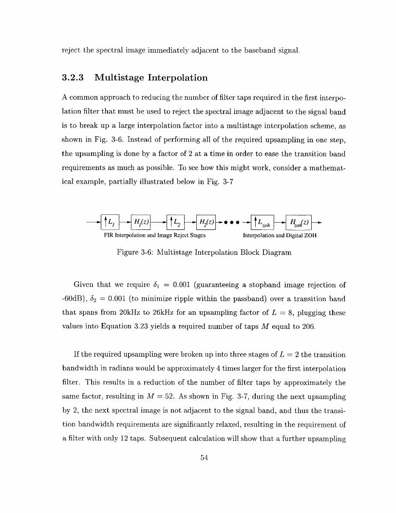
A common approach to reducing the number of filter taps required in the first interpo-
lation filter that must be used to reject the spectral image adjacent to the signal band
is to break up a large interpolation factor into a multistage interpolation scheme, as
shown in Fig. 3-6. Instead of performing all of the required upsampling in one step,
the upsampling is done by a factor of 2 at a time in order to ease the transition band
requirements as much as possible. To see how this might work, consider a mathemat-
ical example, partially illustrated below in Fig. 3-7
SL, - H,(z) L2 H2(z) so - LzOh Hz)
FIR Interpolation and Image Reject Stages Interpolation and Digital ZOH
Figure 3-6: Multistage Interpolation Block Diagram
Given that we require 61 = 0.001 (guaranteeing a stopband image rejection of
-60dB), 62 = 0.001 (to minimize ripple within the passband) over a transition band
that spans from 20kHz to 26kHz for an upsampling factor of L = 8, plugging these
values into Equation 3.23 yields a required number of taps M equal to 206.
If the required upsampling were broken up into three stages of L = 2 the transition
bandwidth in radians would be approximately 4 times larger for the first interpolation
filter. This results in a reduction of the number of filter taps by approximately the
same factor, resulting in M = 52. As shown in Fig. 3-7, during the next upsampling
by 2, the next spectral image is not adjacent to the signal band, and thus the transi-
tion bandwidth requirements are significantly relaxed, resulting in the requirement of
a filter with only 12 taps. Subsequent calculation will show that a further upsampling
54
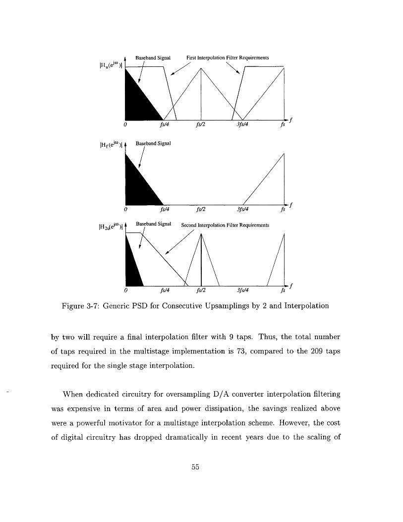
Baseband Sig
IHu(e )I
0 fs/4 fs/2
IHf (e") I Baseband Signal
0 fs/4 fs
H2 e )I Baseband Signal Second I
3fs/4
nterpolation Filter Requirements
0 fs/4 fs/2 3fs/4 fs
Figure 3-7: Generic PSD for Consecutive Upsamplings by 2 and Interpolation
by two will require a final interpolation filter with 9 taps. Thus, the total number
of taps required in the multistage implementation is 73, compared to the 209 taps
required for the single stage interpolation.
When dedicated circuitry for oversampling D/A converter interpolation filtering
was expensive in terms of area and power dissipation, the savings realized above
were a powerful motivator for a multistage interpolation scheme. However, the cost
of digital circuitry has dropped dramatically in recent years due to the scaling of
55
nal First Interpolation Filter Requirements
3fs/4 fs
Ifs/12
. IF
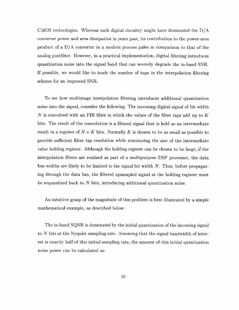
CMOS technologies. Whereas such digital circuitry might have dominated the D/A
converter power and area dissipation in years past, its contribution to the power-area
product of a D/A converter in a modern process pales in comparison to that of the
analog postfilter. However, in a practical implementation, digital filtering introduces
quantization noise into the signal band that can severely degrade the in-band SNR.
If possible, we would like to trade the number of taps in the interpolation filtering
scheme for an improved SNR.
To see how multistage interpolation filtering introduces additional quantization
noise into the signal, consider the following: The incoming digital signal of bit width
N is convolved with an FIR filter in which the values of the filter taps add up to K
bits. The result of the convolution is a filtered signal that is held as an intermediate
result in a register of N + K bits. Normally K is chosen to be as small as possible to
provide sufficient filter tap resolution while minimizing the size of the intermediate
value holding register. Although the holding register can be chosen to be large, if the
interpolation filters are realized as part of a multipurpose DSP processor, the data
bus widths are likely to be limited to the signal bit width N. Thus, before propagat-
ing through the data bus, the filtered upsampled signal at the holding register must
be requantized back to N bits, introducing additional quantization noise.
An intuitive grasp of the magnitude of this problem is best illustrated by a simple
mathematical example, as described below:
The in-band SQNR is dominated by the initial quantization of the incoming signal
to N bits at the Nyquist sampling rate. Assuming that the signal bandwidth of inter-
est is exactly half of this initial sampling rate, the amount of this initial quantization
noise power can be calculated as:
56

2 2 -2N 1Oeinitial 12 OSR (3.25)
but since OSR=1 for the Nyquist-sampled case
0- = -2 (3.26)einitial 12
For the case of the multistage interpolation architecture, quantization noise is
added after each of the upsampling and filtering operations, and thus at each sub-
sequent upsampling stage, the quantization noise is spread over a higher bandwidth.
Hence, the additional quantization noise due to requantization can be calculated as:
2-2N iaestagel = 12 2 (3.27)
2-2N 1+Oetage2 12 4 (3.28)
2-2N i+U1,etg 3 12 8 (3.29)
2 2 -2N 7e -ot = 12 8 (3.30)
The single stage interpolation scheme upsamples the signal by a factor of 8 prior
to filtering and quantization. It thus introduces a noise power of only
2 -2N 1Oetotal 12 8 (3.31)
These two techniques were evaluated in MATLAB for both the multistage and
single stage architectures. The single stage filter was derived by interpolating and
convolving the three filters in the multistage architecture. Thus, the two filter chains
perform exactly the same filtering operations. The results of the MATLAB simulation
are shown in Fig. 3-8 for a 16 bit sinusoidal input at 1171.875 kHz.
57
SNR=98.4ldB for full scale input
16 2 16 H (z) 16 t 2 16 H z 16 2 16 H() 16-
SNR=96.4ldB SNR=96.05dB SNR=96.0ldB
tI8 -- H(Z)
SNR=98.17dB
Figure 3-8: SNR Degradation in Multistage Interpolation Filtering
3.2.4 Postfilter Droop Correction
Because they are implemented in digital hardware, interpolation filters have an inher-
ently robust frequency response, that is to say, the frequency response of the digital
filter will always be exactly the same regardless of any non-critical process variations
within the digital circuitry. Thus, it is often desirable to correct any imperfections
in the analog domain of the D/A converter with compensatory filtering in the digi-
tal domain. Our goal of keeping the analog postfilter circuitry as simple as possible
serves to underscore this point. Although digital interpolation filtering has been pro-
posed to correct for zero order hold droop in D/A converters [18], discussed below is
a compensation technique that is more aggressive and is intended to compensate for
the passband droop induced by the cascade of two first-order filters.
A digital interpolation filter designed using an optimizing algorithm such as the
ones mentioned above produces a filter with a flat passband response containing a
negligible amount of ripple. In order to correct droop in the postfilter, which occurs
primarily in the 10-20kHz region of the passband, it is desirable to have the pass-
band response of the digital interpolation filter to slope upwards at at approximately
the same rate at which the magnitude of the analog postfilter droops in the passband.
This passband droop compensation can be done in an interactive fashion by first
generating the appropriate interpolation filter taps using one of the exchange al-
58
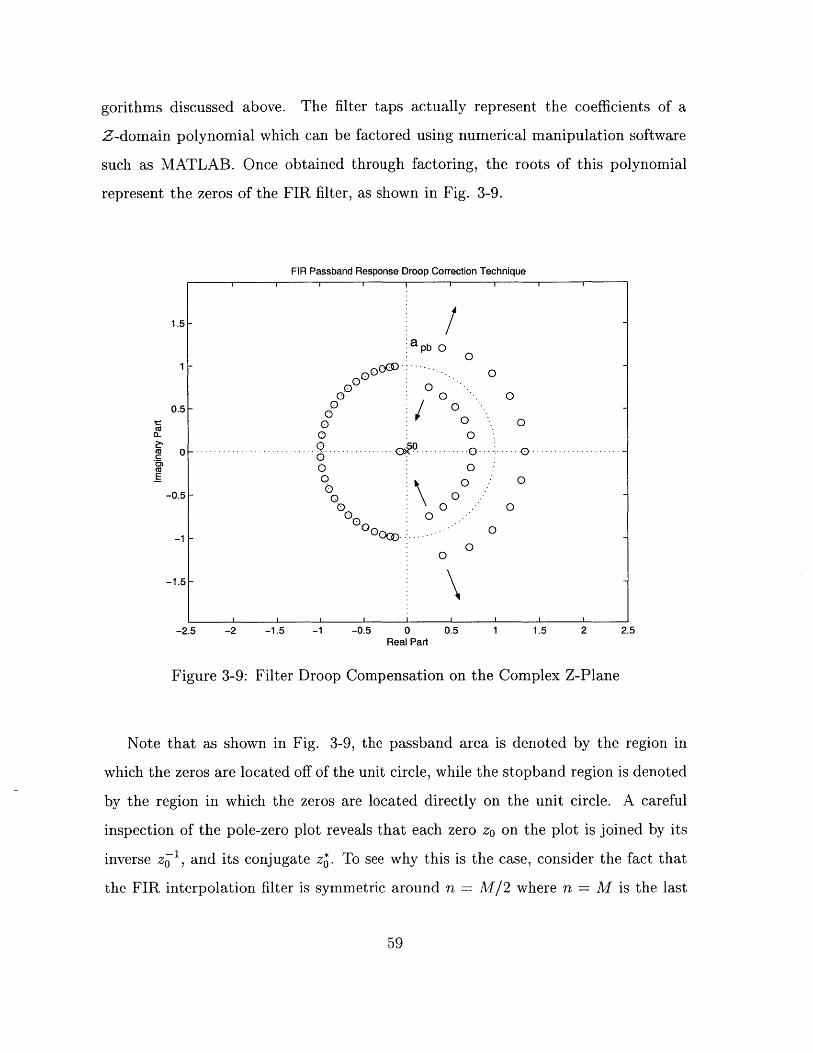
gorithms discussed above. The filter taps actually represent the coefficients of a
Z-domain polynomial which can be factored using numerical manipulation software
such as MATLAB. Once obtained through factoring, the roots of this polynomial
represent the zeros of the FIR filter, as shown in Fig. 3-9.
1.51-
0.51
C3(L
E
0
-0.5
-1
FIR Passband Response Droop Correction Technique
a-aPb 0
0
0 00 0
00 0 00 0*
00
0.. .. .b .. . .. ... . . . .
0
000
o 0 00
F 00 0
00
0
00
0
0
0 -
0
0
0
0
-1.5F
-2.5 -2 -1.5 -1 -0.5 0Real Part
0.5 1 1.5 2 2.5
Figure 3-9: Filter Droop Compensation on the Complex Z-Plane
Note that as shown in Fig. 3-9, the passband area is denoted by the region in
which the zeros are located off of the unit circle, while the stopband region is denoted
by the region in which the zeros are located directly on the unit circle. A careful
inspection of the pole-zero plot reveals that each zero z0 on the plot is joined by its
inverse z-1 , and its conjugate z*. To see why this is the case, consider the fact that
the FIR interpolation filter is symmetric around n = M/2 where n = M is the last
59
1
sample of the filter.
M
H(z)= Z h[n]n=o
(3.32)
but since the filter is symmetric, it is possible to also write
h[n] = h[M - n] (3.33)
and to substitute into the Z-transform equation
M
H(z) = Z h[M - n]Z-"n=O
(3.34)
substituting k = M - n yields
H(z) = h[k]zkz-M = z-MH(z-1 )k=M
(3.35)
Therefore, if zo is a zero, that is, H(zo) = 0, then the above relation holds that:
H(zo) = zoMH(zo1) = 0 (3.36)
Which means that if zo is nonzero, then zO- 1 must also be a zero.
One property of z-transforms holds that in general [4]:
h*[n] = H*(z*) (3.37)
However, since the FIR filter taps are all real,
h[n] = h*[n] (3.38)
and since the FIR filter is designed to have generalized linear phase, it is also true
that
60
H(z) = H eaz(z) -z(2)
H*(z) = Hreai (z) - z /2 = H(z) (3.40)
Thus, it holds that the z-transform of the FIR filter also yields:
H(z*) = H(z) (3.41)
Equation 3.41 implies that if zo is a zero, then z* also is a zero of the FIR filter
polynomial.
In order to perform the postfilter droop compensation, it is necessary to increase
the magnitude of the filter frequency response gradually starting from 10kHz and
peaking at approximately 17.5kHz. In order to do this, it is helpful to examine an
expression for the magnitude of the frequency response as a function of w as the
position of the frequency on the unit circle. This is given by:
JH(edw)12 = H(ejw)H*(ew) = H(z)H*(1/z*)z=ej (3.42)
Given the discussion above regarding the properties of the frequency response of
a generalized linear phase FIR filter, it is possible to write:
M
|H(e")12 = H(z)H(1/z) = |H(z) 2 _ zM = ]I (z - ak)21z=ej (3.43)k=1
Equation 3.43 implies that the magnitude of the FIR frequency response at a given
frequency is equal to the product of the position of that frequency mapped onto the
unit circle to each of the zeros in the Z-plane. In a system that has a frequency re-
sponse such as that of an FIR filter, the magnitude at any given frequency is largely
determined by those zeros closest to that frequency. For example, while moving along
the unit circle near the zero denoted apb in the FIR passband whose magnitude is
61
(3.39)
greater than unity and whose angle is most positive, the magnitude of the distance
of the frequency mapped to the unit circle to apb is much smaller than the distances
to the other zeros ak. In addition, moving slightly on the unit circle changes the
magnitude of the distance to apb while the magnitudes of the distances to other zeros
ak remain relatively unaffected.
Based on the above discussion, one method to increase the magnitude of the
frequency response at the frequencies close to passband edge would be to increase
the distance of the zero apb from the unit circle. This can be done by scaling the
magnitude, but leaving the angle unchanged, of the zero apb outside of the unit circle
by a factor (1 + 6). Of course, in order for the FIR filter to retain the property of
generalized linear phase, the zero 1/apb on the inside of the unit circle must have its
magnitude scaled by 1/(1 +6) in order to remain the inverse of the modified zero apb.
In addition, the magnitude of the zero a*b must be scaled by the factor (1 +6) and its
inverse zero scaled by 1/(1 + 6). The frequency response of the resultant FIR filter is
shown in Fig. 3-10. When placed in the D/A converter system, the overall frequency
response is corrected to have a relatively flat passband, as shown in Fig. 3-11.
3.2.5 Digital Zero Order Hold Interpolation
The remainder of the interpolation done after the final upsampling after the interpo-
lation filtering chain is performed by a digital zero-order hold register. As shown in
Fig. 3-12, the digital zero-order hold simply interpolates between upsampled values
by repeating the original sample P times. Like the zero-order hold mentioned in the
discussion on the DT-CT interface, this digital zero-order hold introduces a slight
frequency domain droop in the signal band; however, if the rate at which the signal
is upsampled is on the order of 10, this droop is negligible and could at any rate be
corrected by the same postfilter droop compensation technique discussed earlier. The
sinc filter response of the zero-order hold also attenuates the spectral images intro-
62
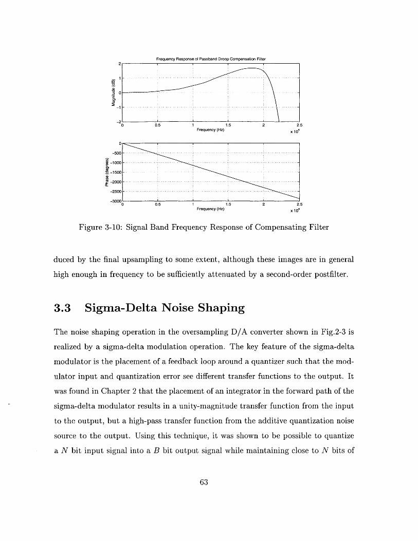
Frequency Response of Passband Droop Compensation Filter
0 -- -.-- -.-.---.- -. .-- -
a-2
0 0.5 1 1.5 2 2.5Frequency (Hz) x, 1
0
- 5 0 0 - - -.. . -. --.. . - - -.. . -. .-. -. .-.-.-.-.-.-.-.-.-.- -
-1000 -g- - a- Frequency - R-s-p-n-s- of Comensti - -
S -1500 -- -. - -.. . . . . . . . . . . . . . .-
0 -2 0 0 0 -. - -. . -. -.. . . . . -. . . .-..-.-.-..-.-.- -..-.- -
- 2 5 0 0 - -. . - - - . . . . . .-. ..- - -- - - - - - -- - - -. . .
->00 0.5 1.5 22.5Frequency (Hz) x 10
Figure 3-10: Signal Band Frequency Response of Compensating Filter
duced by the final upsampling to some extent, although these images are in general
high enough in frequency to be sufficiently attenuated by a second-order postfilter.
3.3 Sigma-Delta Noise Shaping
The noise shaping operation in the oversampling D/A converter shown in Fig.2-3 is
realized by a sigma-delta modulation operation. The key feature of the sigma-delta
modulator is the placement of a feedback loop around a quantizer such that the mod-
ulator input and quantization error see different transfer functions to the output. It
was found in Chapter 2 that the placement of an integrator in the forward path of the
sigma-delta modulator results in a unity-magnitude transfer function from the input
to the output, but a high-pass transfer function from the additive quantization noise
source to the output. Using this technique, it was shown to be possible to quantize
a N bit input signal into a B bit output signal while maintaining close to N bits of
63
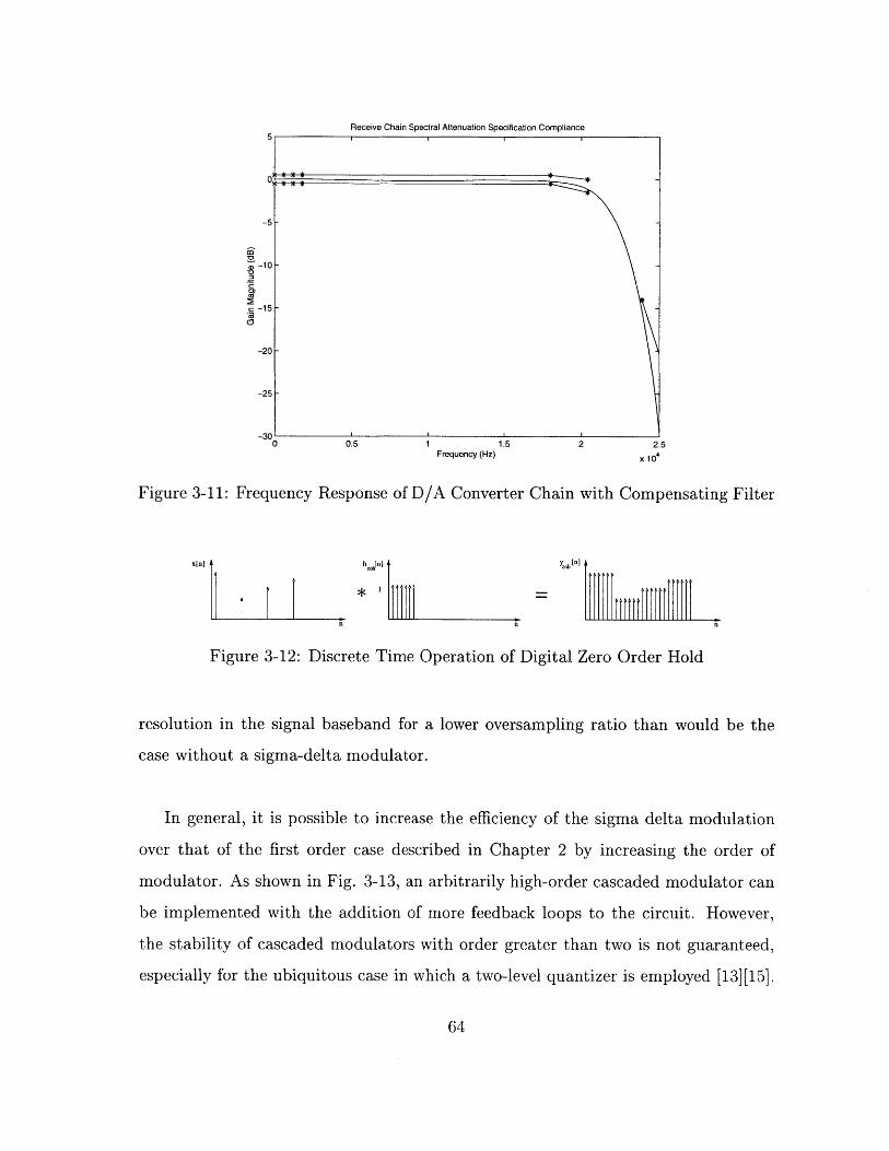
Receive Chain Spectral Attenuation Specification Compliance
-10-a
et - 10
c-15--
-20-
-25-
-3010 0.5 1 1.5 2 2.5
Frequency (Hz) x 10
Figure 3-11: Frequency Response of D/A Converter Chain with Compensating Filter
xtn h jn Y l[n]
Figure 3-12: Discrete Time Operation of Digital Zero Order Hold
resolution in the signal baseband for a lower oversampling ratio than would be the
case without a sigma-delta modulator.
In general, it is possible to increase the efficiency of the sigma delta modulation
over that of the first order case described in Chapter 2 by increasing the order of
modulator. As shown in Fig. 3-13, an arbitrarily high-order cascaded modulator can
be implemented with the addition of more feedback loops to the circuit. However,
the stability of cascaded modulators with order greater than two is not guaranteed,
especially for the ubiquitous case in which a two-level quantizer is employed [13][15].
64
0
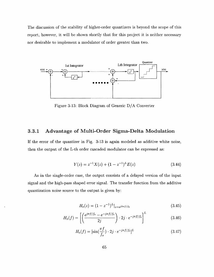
The discussion of the stability of higher-order quantizers is beyond the scope of this
report, however, it will be shown shortly that for this project it is neither necessary
nor desirable to implement a modulator of order greater than two.
Quantizer
1st Integrator Lth Integratorx + \ + y(n)
+ +
Z ++
Figure 3-13: Block Diagram of Generic D/A Converter
3.3.1 Advantage of Multi-Order Sigma-Delta Modulation
If the error of the quantizer in Fig. 3-13 is again modeled as additive white noise,
then the output of the L-th order cascaded modulator can be expressed as:
Y(z) = z-X(z) + (1 - z-)L E(z) (3.44)
As in the single-order case, the output consists of a delayed version of the input
signal and the high-pass shaped error signal. The transfer function from the additive
quantization noise source to the output is given by:
He(Z) = (1 - Zl-)L z=ej2f//fs (3.45)
He(f) [(e=fs. _-7rf/f. 2j - e-If-L (3.46)
He(f) = [sin( 2j e--f/fs]L (3.47)fS
65
Taking the magnitude of both sides, we obtain the high pass transfer function:
|He(f)I = (2sin(L)L (3.48)fS
Recalling that the power spectral density of the unshaped additive quantization
noise in an oversampled system is expressed as:
2 A 2
Se(f) = (3.49)12 fs
it is possible to obtain the power spectral density of the shaped noise by multiply-
ing the power spectral density of the unshaped quantization noise with the square of
the magnitude of the noise shaping function. The inband shaped noise power is then
obtained by integrating the power spectral density across the two-sided signal band.
This operation is expressed as:
Se(f)IHe(f) A2 1 2L
Pe =, S2 12 (H 2[2 sin( )]2 Ldf (3.50)
Assuming that fo << f8, it is possible to approximate that sin(7rf/f,) e wrf/f,
over the signal band. Performing the integral with the approximation noted above
yields:
P ,2) i 2L+l 7r2L
e 12 OSR 2L +1 (.1
Assuming that the maximum SNR is obtained with a sinusoidal input, it is possible
to develop an expression for the maximum SNR available to an Lth-order modulator
for a given oversampling ratio.
SNRmax = 10log(Ps/Pe) = 1010g0( 322N) + 101og 1 0 [2L + (OSR)2L+] (3.52)
SNRmax = 6.02N + 1.76 + 10 logiO(2L + 1) - 9.94L + 10(2L + 1) logio(OSR) (3.53)
66
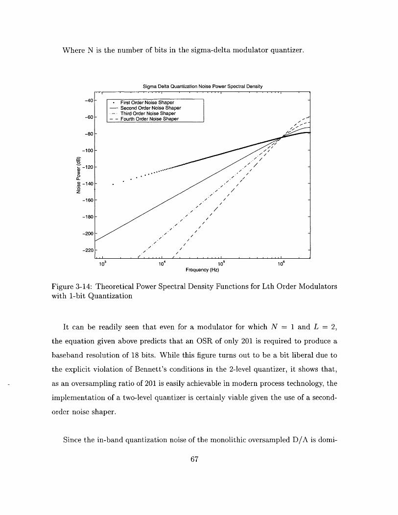
Where N is the number of bits in the sigma-delta modulator quantizer.
Sigma Delta Quantization Noise Power Spectral Density
-40*
-60
-80
-100
-120
0
0
- 160
-180
-200
-220
105
Frequency (Hz)106
Figure 3-14: Theoretical Power Spectral Density Functions for Lth Order Modulatorswith 1-bit Quantization
It can be readily seen that even for a modulator for which N = 1 and L = 2,
the equation given above predicts that an OSR of only 201 is required to produce a
baseband resolution of 18 bits. While this figure turns out to be a bit liberal due to
the explicit violation of Bennett's conditions in the 2-level quantizer, it shows that,
as an oversampling ratio of 201 is easily achievable in modern process technology, the
implementation of a two-level quantizer is certainly viable given the use of a second-
order noise shaper.
Since the in-band quantization noise of the monolithic oversampled D/A is domi-
67
- First Order Noise Shaper- Second Order Noise Shaper
- - Third Order Noise Shaper- -- Fourth Order Noise Shaper
--
//
.
- -
/ -
.I .1 . . . . ..:I. . . . . . . . I:|| r
10 3 10 4
nated by the initial quantization of the input signal to N bits, we only require that the
signal band resolution of the sigma-delta modulator be on the order of N +2 - N +3
such that the noise it introduces is negligible. In industry audio applications, a typ-
ical value for N is 16, meaning that a second order modulator operating at an OSR
on the order of 100 will satisfy the above condition. As will be discussed in Section
4.4, it is also required to operate at a high oversampling ratio to reduce the effects of
clock jitter at the DT-CT interface. Clock jitter contributes noise to the signal and
increases as the OSR decreases. Its effects also turn out to constrain the OSR to be
greater than 100. In addition, as the order of sigma-delta modulation is increased,
the amount of out-of-band noise also increases as a result of the noise shaping opera-
tion. This requires a higher order analog postfilter to attenuate. Since it is desirable
to minimize the order of the analog postfilter, it is hence also desirable to keep the
order of the sigma-delta modulator as small as possible while still meeting the design
objectives. As is evident, a sigma-delta modulator of order 2 represents a reasonable
compromise between the aforementioned objectives.
3.3.2 Single Bit vs. Multibit Modulation
Single-bit, or two-level, quantizers are a popular choice in contemporary D/A con-
verter design because of their inherent linearity. A misplacement of one level as a
result of device mismatch only changes the quantization range and DC offset, neither
of which are critical in a differential postfiltering application [13]. However, because
only having two levels of quantization with a step size A equal to its output range
seriously violates the conditions set forth to make the additive white quantization
noise approximation, the single-bit modulator has serious drawbacks.
First, consider the application of a DC input to a first-order modulator with a
two-level quantizer. We know that the gain of the digital integrator in the modulator
at DC is infinite and thus the average value of the output that is fed back to this in-
68
tegrator must equal the DC value of the input. In general, the sigma-delta modulator
will output a periodic sequence of is and -Is whose time-averaged value equals the
value of the DC input. Since the sequence is periodic, it has a small amount of power
concentrated at the frequency corresponding to the period of the sequence used to
represent the DC input. This concentration of frequency is referred to as tonal behav-
ior in the modulator and is extremely undesirable, as the human ear is very sensitive
to such tones. [3]. One way to reduce the effect of these tones is to deliberately add
a pseudorandom digital noise source in the sigma-delta modulator. This technique,
known as dithering, can add enough randomness to the quantizer input to break up
the periodic behavior of the quantizer output signal.
This additive pseudorandom digital noise source is normally placed immediately
before the quantizer such that the pseudorandom dither noise is shaped along with
the quantization noise. Although this technique can usually reduce the presence of
tones to acceptable levels, it increases the quantization noise floor of the modulator,
thus requiring a higher oversampling ratio to achieve a desired signal band resolution.
For a given order of sigma-delta modulation and a given oversampling ratio, multi-
bit topologies provide about 6dB more in-band SNR per bit over a 1 bit implemen-
tation. Because of their superior noise performance, multibit topologies have become
more popular in D/A architectures in recent years. Since they produce less in-band
noise than their single-bit, use of a multibit modulator permits the reduction of the
oversampling ratio while still maintaining the same SNR. As is described later in the
discussion on switched-capacitor filtering, reducing the oversampling ratio is critical
in achieving low analog die area consumption.
In addition, multibit D/A topologies more closely meet the Bennett quantization
noise approximation conditions. Because of this, multibit D/As realize a dramatic
69
reduction of in-band idle tones without the use of dither and achieve greater loop
stability for higher-order modulators. [13][17] However, multibit sigma-delta modu-
lators rely on multibit D/A architectures that consist of an array of passive elements.
As the matching of these elements corresponds to a resolution of 10-12 bits, some
form of dynamic element matching or element calibration is necessary to improve
the linearity of the D/A converter element array. In general, both techniques require
digital overhead circuitry that increases in complexity proportional to 2B. Since this
circuitry must be implemented in dedicated hardware on the analog die, it is desirable
to keep B small to minimize digital power and area consumption.
In the context of power and area optimizing the oversampling D/A converter it
is important to consider the maximum amplitude signal that can pass through the
sigma-delta modulator without overloading the quantizer. The attentive reader will
recall from Chapter 2 that if the gain of the noise shaper must decrease in order to
accommodate the signal, any noise introduced after the sigma-delta modulator will
have a more adverse effect on the SNR than it would if the signal magnitude at the
output of the sigma-delta were greater. In a sigma-delta modulator, the oscillation
of the signal within the modulator uses up some of the dynamic range of the circuit,
causing the quantizer to overload if the input amplitude is not limited. [13] Simu-
lation results from MATLAB shown in Fig. 3-15 give the maximum available input
amplitude as a function of number of quantizer bits for a second order cascaded mod-
ulator. As intuition might suggest, as the number of bits B increases, the dynamic
range asymptotically approaches unity.
3.3.3 Implementation of a Sigma-Delta Modulator
The sigma-delta modulator implemented in this project was first designed as a be-
havioral model, then implemented as an equivalent digital block in combinational
logic. The second-order modulator behavioral model was implemented as shown in
70
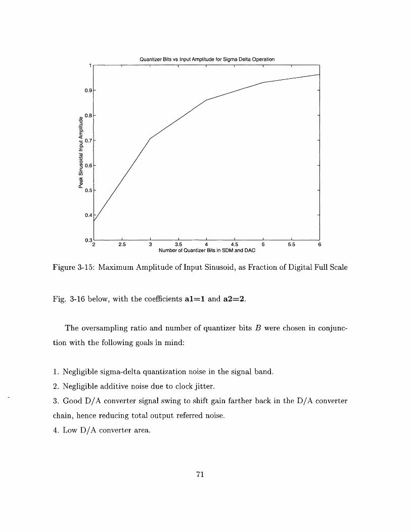
Quantizer Bits vs Input Amplitude for Sigma Delta Operation
0.9-
0.8-
E0.7-
0.
0.6 --CZ
0.5-
0.4-
S0.6
2 2.5 3 3.5 4 4.5 5 5.5 6Number of Quantizer Bits in SDM and DAC
Figure 3-15: Maximum Amplitude of Input Sinusoid, as Fraction of Digital Full Scale
Fig. 3-16 below, with the coefficients a1=1 and a2=2.
The oversampling ratio and number of quantizer bits B were chosen in conjunc-
tion with the following goals in mind:
1. Negligible sigma-delta quantization noise in the signal band.
2. Negligible additive noise due to clock jitter.
3. Good D/A converter signal swing to shift gain farther back in the D/A converter
chain, hence reducing total output referred noise.
4. Low D/A converter area.
71
1
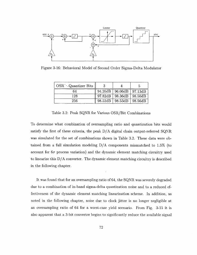
Limiter Quantizer
Figue 3 + y(n)
a~a 2
Figure 3-16: Behavioral Model of Second Order Sigma-Delta Modulator
OSR .Quantizer Bits 3 1 4 1 5 1 ]64 94.20dB 96.06dB 97.13dB128 97.82dB 98.36dB 98.50dB256 98.52dB 98.53dB 98.56dB
Table 3.2: Peak SQNR for Various OSR/Bit Combinations
To determine what combination of oversampling ratio and quantization bits would
satisfy the first of these criteria, the peak D/A digital chain output-referred SQNR
was simulated for the set of combinations shown in Table 3.2. These data were ob-
tained from a full simulation modeling D/A components mismatched to 1.5% (to
account for 6a- process variation) and the dynamic element matching circuitry used
to linearize this D/A converter. The dynamic element matching circuitry is described
in the following chapter.
It was found that for an oversampling ratio of 64, the SQNR was severely degraded
due to a combination of in-band sigma-delta quantization noise and to a reduced ef-
fectiveness of the dynamic element matching linearization scheme. In addition, as
noted in the following chapter, noise due to clock jitter is no longer negligible at
an oversampling ratio of 64 for a worst-case yield scenario. From Fig. 3-15 it is
also apparent that a 3-bit converter begins to significantly reduce the available signal
72
swing at the output of the sigma-delta modulator. (at the time of the sigma-delta
modulator design, it was thought that this signal swing would even be too small to
meet the overall signal swing requirements for a postfilter gain of unity). For a large
OSR and number of quantization bits, the vast majority of the noise introduced by
the sigma-delta modulator exists outside of the signal band, while the noise still in
the signal band is negligible compared to the quantization noise introduced by the
initial 16-bit and digital interpolation filtering quantizations.
Thus, a sigma-delta modulator with OSR=128 and B=4 was chosen to obtain
a close to optimal in-band SQNR and good signal swing, with the minimal OSR and
number of D/A converter components necessary to achieve this performance. Note
that the numbers given in Table 3.2 are greater than that given in Fig. 3-8 because
postfilter droop compensation in the interpolation filter chain magnifies the noise in
the lOkHz-2OkHz range, however, this noise is then attenuated by and equal amount
by the postfilter droop.
The behavioral model of the resultant sigma-delta modulator design, in addition
to the implemented version, accepts as its input the 16-bit output of the digital zero
order hold multiplied by 1.625. The area and power consumed by this multiplication
is minimal in that it consists of adding the 16-bit signal to itself, downshifted by 1
bit, and to itself again, this time downshifted by 3 bits. Since the sigma-delta modu-
lator has an input bit width of 17 bits, this corresponds to an effective attenuation of
the signal by 0.8125, but without introducing truncation noise. This is attenuation is
necessary so as to allow a full scale signal from the interpolation chain to pass through
the 4-bit sigma-delta modulator without causing the modulator to go into overload.
The performance of the digital interpolation chain terminated by the sigma-delta
modulator and analog postfilter is shown in Fig. 3-17, where the magnitude of the
73
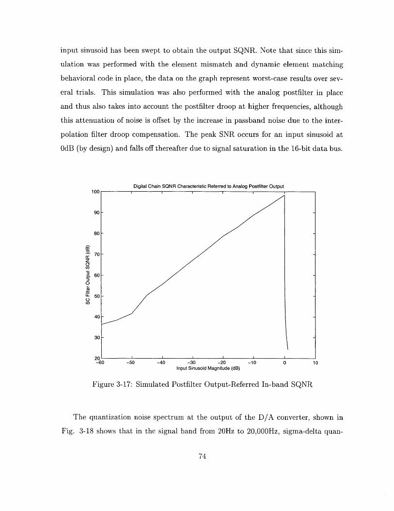
input sinusoid has been swept to obtain the output SQNR. Note that since this sim-
ulation was performed with the element mismatch and dynamic element matching
behavioral code in place, the data on the graph represent worst-case results over sev-
eral trials. This simulation was also performed with the analog postfilter in place
and thus also takes into account the postfilter droop at higher frequencies, although
this attenuation of noise is offset by the increase in passband noise due to the inter-
polation filter droop compensation. The peak SNR occurs for an input sinusoid at
OdB (by design) and falls off thereafter due to signal saturation in the 16-bit data bus.
Digital Chain SQNR Characteristic Referred to Analog Postfilter Output
Z
aC')
0
C')
1 UU
90
80
70
60
50
40
301-
-60 -50
Figure 3-17: Simul
-40 -30 -20 -10-40 -30 -20 -10
Input Sinusoid Magnitude (dB)
ated Postfilter Output-Referred
0
The quantization noise spectrum at the output of the D/A converter, shown in
Fig. 3-18 shows that in the signal band from 20Hz to 20,000Hz, sigma-delta quan-
74
10
In-band SQNR
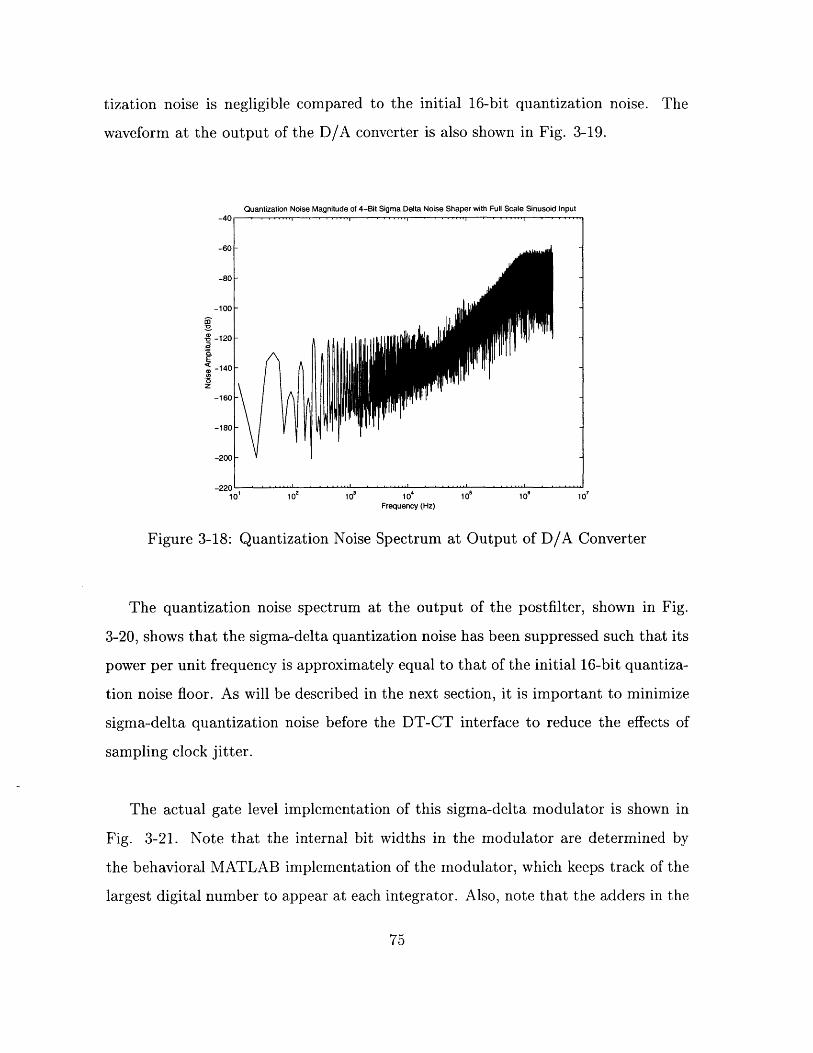
tization noise is negligible compared to the initial 16-bit quantization noise. The
waveform at the output of the D/A converter is also shown in Fig. 3-19.
Quantization Noise Magnitude of 4-Bit Sigma Delta Noise Shaper with Full Scale Sinusoid Input
10 10, 104Frequency (Hz)
10, 10 10
Figure 3-18: Quantization Noise Spectrum at Output of D/A Converter
The quantization noise spectrum at the output of the postfilter, shown in Fig.
3-20, shows that the sigma-delta quantization noise has been suppressed such that its
power per unit frequency is approximately equal to that of the initial 16-bit quantiza-
tion noise floor. As will be described in the next section, it is important to minimize
sigma-delta quantization noise before the DT-CT interface to reduce the effects of
sampling clock jitter.
The actual gate level implementation of this sigma-delta modulator is shown in
Fig. 3-21. Note that the internal bit widths in the modulator are determined by
the behavioral MATLAB implementation of the modulator, which keeps track of the
largest digital number to appear at each integrator. Also, note that the adders in the
75
-60
-80 -
-100
S-120
-140
V- 160
-180
-200
71,11
y - I
10
W1 1 11
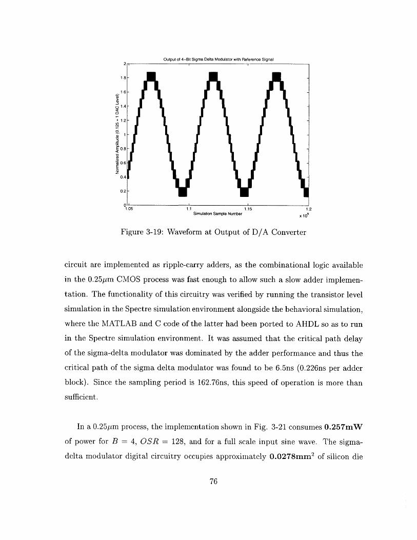
Output of 4-Bit Sigma Delta Modulator with Reference Signal
.2 - -
1.8-
1.6-
1.4
1.2 -
S6
0.4
0.2
1.05 1.1 1.15 1.2Simulation Sample Number x10
Figure 3-19: Waveform at Output of D/A Converter
circuit are implemented as ripple-carry adders, as the combinational logic available
in the 0.25pm CMOS process was fast enough to allow such a slow adder implemen-
tation. The functionality of this circuitry was verified by running the transistor level
simulation in the Spectre simulation environment alongside the behavioral simulation,
where the MATLAB and C code of the latter had been ported to AHDL so as to run
in the Spectre simulation environment. It was assumed that the critical path delay
of the sigma-delta modulator was dominated by the adder performance and thus the
critical path of the sigma delta modulator was found to be 6.5ns (0.226ns per adder
block). Since the sampling period is 162.76ns, this speed of operation is more than
sufficient.
In a 0.25pm process, the implementation shown in Fig. 3-21 consumes 0.257mW
of power for B = 4, OSR = 128, and for a full scale input sine wave. The sigma-
delta modulator digital circuitry occupies approximately 0.0278mm 2 of silicon die
76
area. In addition, one 15-bit adder and one 17-bit adder are required to perform the
multiplication by 1.625. These adders consume approximately 0.0085mm 2 of silicon
die area and consume approximately 0.1mW of power. One can expect the power
consumption of this circuitry to increase linearly with OSR.
3.3.4 Alternative Architectures
Before concluding this discussion, it is appropriate to note that the cascaded sigma-
delta modulator described above is not the only structure capable of realizing a noise
shaping operation. In Fig. 3-22 below, an error feedback structure is depicted [16].
Using the same linear Z-domain analysis used for the cascaded modulator, it can be
seen that the transfer function from the input x[n] to the output y[n] is unity, while
the transfer function from the quantizer to the output is equal to G(z) Thus, choosing
G(z) to be (1 - z-1)L by choosing the appropriate combination of delay blocks and
scaling coefficients for G(z) - 1 results in a transfer function identical to that of the
cascaded structure.
77
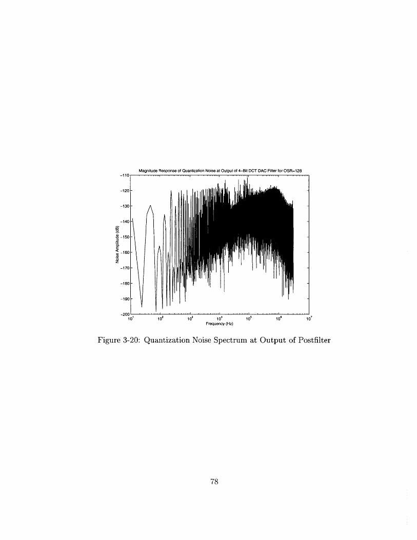
Magnitude Response of Quantization Noise at Output of 4-Bit DCT DAC Filter for OSR=128
- . I - i l i Ii -1i 1'-. -l " '
10' 10 10 104
Frequency (Hz)10, 10 10
Figure 3-20: Quantization Noise Spectrum at Output of Postfilter
78
-110
-120-
-130
-140
z
-150
-160
-170
-180
-1901
-9no
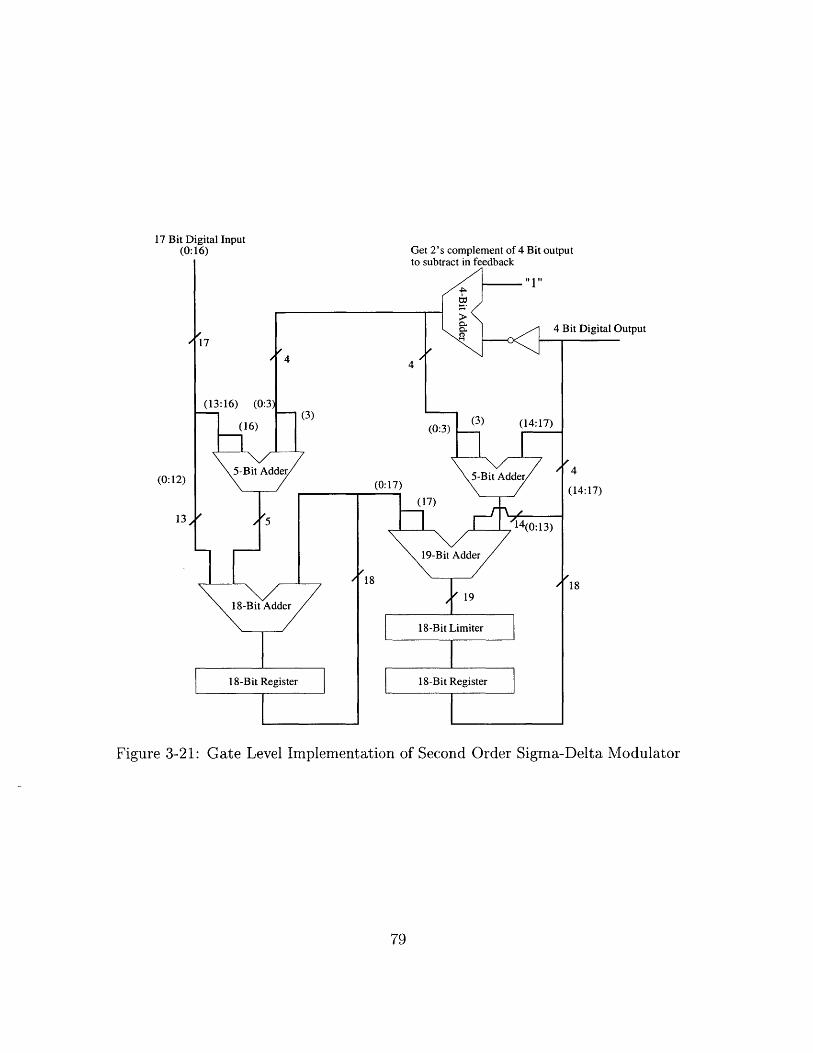
17 Bit Digital Input(0:16)
(0:12)
13 d
17
Get 2's complement of 4 Bit outputto subtract in feedback
4 BitDigital Output
44
(13:16) (0:3)(3)
(16) (
5-Bit Adder
5
18-Bit Adder
18-Bit Register
(:) (3) (14:17)
(0:17) 5-Bit Adder
(17)
14(0:13)
19-Bit Adder
18
19 /
18-Bit Limiter
18-Bit Register
Figure 3-21: Gate Level Implementation of Second Order Sigma-Delta Modulator
79
4
(14:17)
18
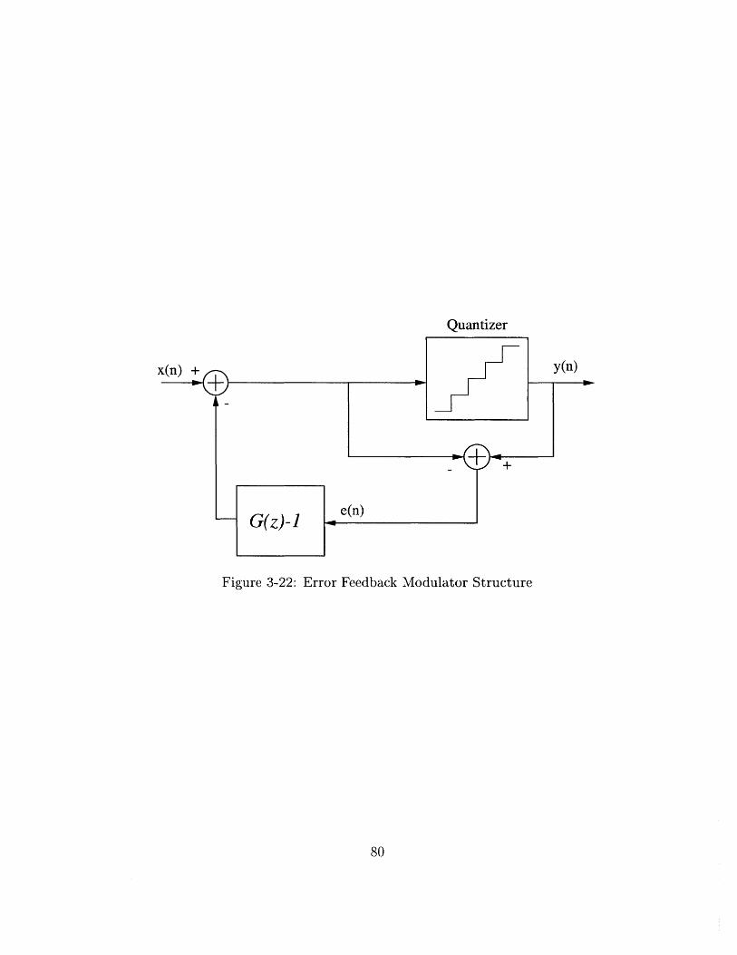
x(n) +
-G(z)-1 ~-
Quantizer
y(n)
~n)
Figure 3-22: Error Feedback Modulator Structure
80
Chapter 4
Oversampled D/A Converter
Topologies
Various literatures in the past have reported on the suitability of particular D/A ar-
chitectures for low power applications[5][21]. The optimal architecture, however, may
depend on a number of subtle requirements of the specific application. For example,
the D/A converter described in this document is constrained by a number of unique
factors.
The first of these is the requirement that the frequency response of the D/A con-
verter and its analog postfilter scale in bandwidth automatically with the frequency
of the incoming clock waveform. In order to optimize power usage, the D/A con-
verter and its postfilter should operate only at the bandwidth required to produce
the desired audio quality. Therefore, when the phone outputs voice quality audio,
the bandwidth should be 4kHz, while music quality audio should have a bandwidth
of 24kHz (although all noise measurements are specified over the 20Hz-2OkHz band).
The second requirement is that the output of the D/A converter chain postfilter be
a voltage signal, implying that the output of any current-mode D/A converter be
passed through an current-to-voltage converter. Finally, all of the DAC and post-
81
filter components must be implemented on-chip. As off-chip filtering introduces the
possibility of external noise coupling and adds cost in the form of additional discrete
components, it is undesirable in applications that demand good noise performance
and low board space consumption.
4.1 Current-Mode Topologies
Current-mode D/A topologies generate an analog output waveform by using the dig-
ital sigma-delta modulator output to switch an array of current sources to either
the D/A summing junction or to ground (or to the inverted summing junction in a
differential implementation as shown in Fig. 4-1). Current mode architectures have
become popular in many applications because the alternative, a switched-capacitor
D/A followed by an integrated switched-capacitor postfilter has a severe tradeoff be-
tween the noise power, capacitor area, and power dissipation. [12] The rationale is
that to achieve low kT/C noise in the postfilter, large capacitors are needed, consum-
ing area. In addition, opamps with high output stage current, and hence higher power
dissipation, are required to drive these larger capacitances [12]. It also has been re-
ported that for D/A converters requiring bandwidths in the MHz range, current-mode
converters provide superior dynamic performance over switched-capacitor topologies
[5].
Current-mode converters also retain their share of disadvantages. For example,
their current-mode output is susceptible to intersymbol interference [3], the condition
in which the rise and fall times of the output waveform are not equal. When this
is the case, the integral of the output waveform over a given output symbol's time
period will be dependent on the value of the previous symbol. Often, this drawback
requires particular attention in the design of the output elements [12] in order to
avoid serious distortion in the output waveform. In addition, attention must be paid
82
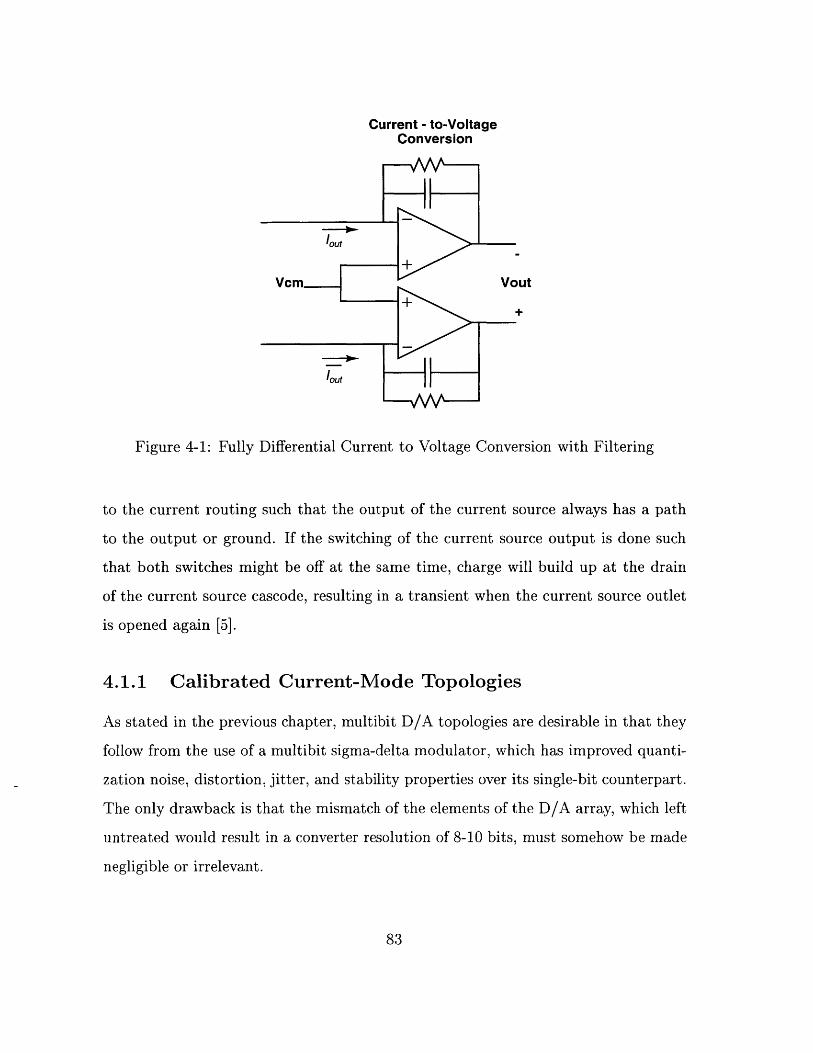
Current - to-VoltageConversion
VCM Vout
lout
Figure 4-1: Fully Differential Current to Voltage Conversion with Filtering
to the current routing such that the output of the current source always has a path
to the output or ground. If the switching of the current source output is done such
that both switches might be off at the same time, charge will build up at the drain
of the current source cascode, resulting in a transient when the current source outlet
is opened again [5].
4.1.1 Calibrated Current-Mode Topologies
As stated in the previous chapter, multibit D/A topologies are desirable in that they
follow from the use of a multibit sigma-delta modulator, which has improved quanti-
zation noise, distortion, jitter, and stability properties over its single-bit counterpart.
The only drawback is that the mismatch of the elements of the D/A array, which left
untreated would result in a converter resolution of 8-10 bits, must somehow be made
negligible or irrelevant.
83
For applications in which Dynamic Element Matching, the alternative lineariza-
tion method to be discussed later in this chapter, is not feasible, such as those which
cannot support the high oversampling ratio required for DEM to be effective, calibra-
tion techniques present an attractive alternative. A calibrated current-mode topology
consists of an array of 2B 1 switched current sources, whose routing switches accept
as their inputs the thermometer-encoded output bits of the B sigma-delta modulator
outputs. Each array element appears as shown in the simplified schematic below in
Fig. 4-2 and consists of both a fine current source and a coarse current source. The
coarse source will be biased such that its output is some fraction 1 - k of a reference
current Ief where k is typically less than 0.2. Of course, each of these coarse current
sources will be mismatched to the effect of 8-10 bits.
The fine current source is dynamically biased to conduct the difference of the
coarse current source and ',ef. Thus, on average, a fine current source will con-
duct klef immediately after dynamic biasing, or calibration. For each of the 2B + 1
cycles of operation, one of the array elements is taken out of the array of 2B func-
tioning elements to be calibrated. Taking its place will be the element that has just
been calibrated. During calibration, switch S2 will close and a reference current ref
will be forced into the parallel combination of the coarse and fine current sources.
(1 - k - mismatch)Iref will flow into the coarse current source, while the remain-
der flows into the fine current source, which is diode-connected in this configuration.
Based on the current flowing through it, a voltage develops on the gate-source capac-
itance of the fine current source such that when the array element is taken out of the
calibration configuration, the voltage remains on the gate of the fine current source.
Since this voltage remains roughly the same over the cycle of operation in which the
element is part of the D/A array, the overall element will conduct an amount of cur-
rent very close to Iref.
84
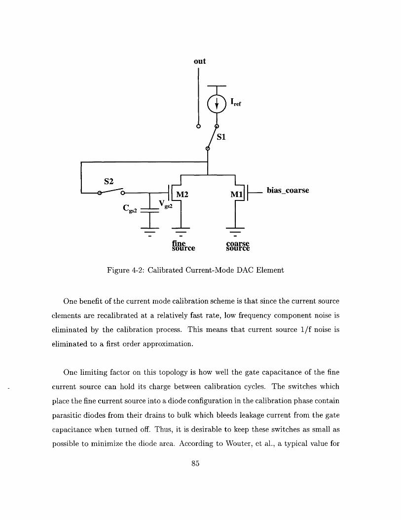
out
Iref
S1
S2
M2 Ml biascoarse
fine coarsesource source
Figure 4-2: Calibrated Current-Mode DAC Element
One benefit of the current mode calibration scheme is that since the current source
elements are recalibrated at a relatively fast rate, low frequency component noise is
eliminated by the calibration process. This means that current source 1/f noise is
eliminated to a first order approximation.
One limiting factor on this topology is how well the gate capacitance of the fine
current source can hold its charge between calibration cycles. The switches which
place the fine current source into a diode configuration in the calibration phase contain
parasitic diodes from their drains to bulk which bleeds leakage current from the gate
capacitance when turned off. Thus, it is desirable to keep these switches as small as
possible to minimize the diode area. According to Wouter, et al., a typical value for
85
this leakage current would be on the order of [213:
Ileak = O.0lWswitchLdiff A (4.1)
Assuming that the calibration of a current source is done at time t=0, the gate
voltage equals:
Vgs,leak -- V s- Ieak t (4.2)cgs
at any given time t until the next calibration cycle.
Another source of nonideality between array elements is charge injection from the
switches used to diode-configure the fine current sources. Although charge-cancelling
techniques can be used to lessen the effect of charge injection, in general about 1/10th
of the channel charge will still end up on the gate of the fine current source MOSFET.
In addition, it is reasonable to assume that for such a switch, the charge injected from
the switch will be mismatched on the order of 10%. This switch should be a CMOS
transistor to avoid threshold voltage effects, and the PMOS and NMOS transistors
should be sized the same so that their channel charges cancel to a large extent upon
switch turn-off.
Thus,
Aqch = 0.1 CoxWswitchLswitch Veffswitch (43)10
,AVgs,q - Aqch (4.4)Cgs
The changes in the gate voltage of the MOSFET are transformed into changes in
the fine current source drain current by its transconductance. Thus, we would like to
86
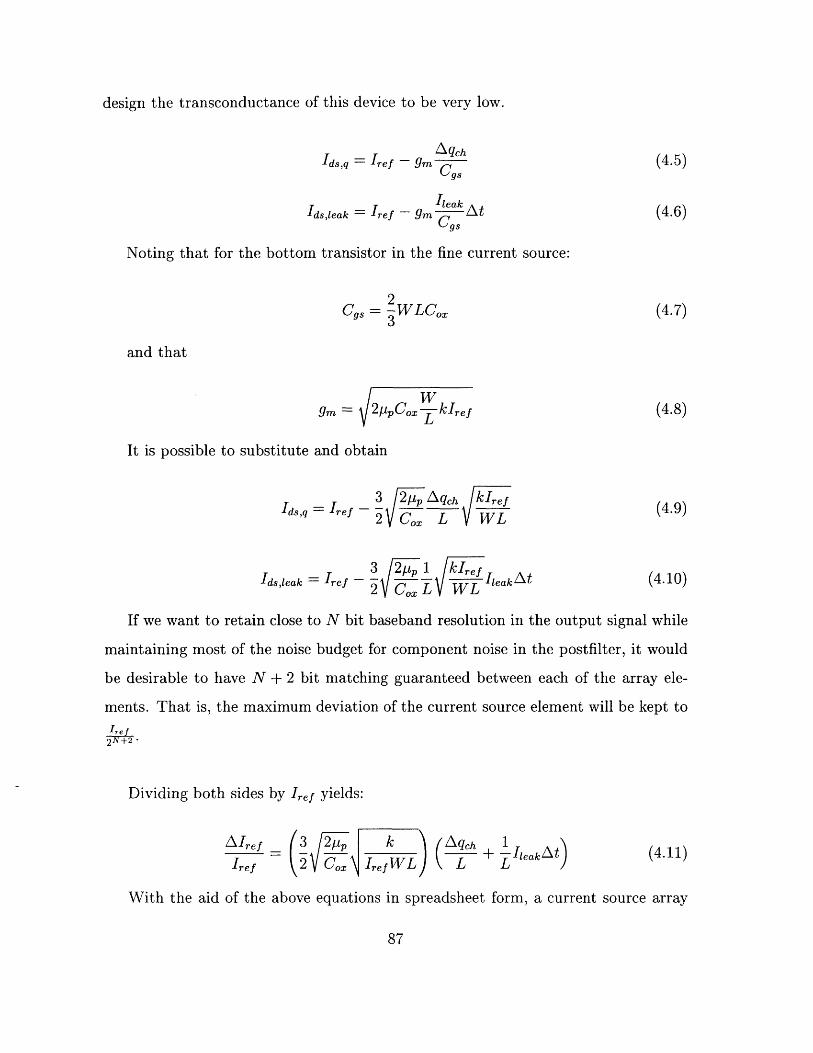
design the transconductance of this device to be very low.
Idsq = 'ref - gm Aqeh (4.5)Mcgs
Ids,leak = Iref - gm 'leak At (4.6)cgs
Noting that for the bottom transistor in the fine current source:
2Cgs = -WLCox (4.7)
3
and that
W9M = 2ppCox L kIref (4.8)
It is possible to substitute and obtain
3 2pp, /.qch krf(4.9)Ids,q= Iref -2c L WL
Ids,leak Iref - k 2 L ref Ileak At (4.10)
If we want to retain close to N bit baseband resolution in the output signal while
maintaining most of the noise budget for component noise in the postfilter, it would
be desirable to have N + 2 bit matching guaranteed between each of the array ele-
ments. That is, the maximum deviation of the current source element will be kept toIre!
Dividing both sides by Iref yields:
A-Tref 3 /2pp k Aqch If= (3 +Ie LeakJAt (4.11)
Iref 2 v Coxs Iren L L L
With the aid of the above equations in spreadsheet form, a current source array
87
with 16 elements (B=4), W=15pm, L=150pm, Co ,=0.006384y, jpp=0.0064223 ,
k=0.2, 2 B =16 , and with a minimum sized calibration switch of W=0.5pm, L=0.25pim,
and VeffO0.5V was designed. Note that for these parameters, the time constant of
the fine current source transistor is given by:
2T = Rswitch WLCox (4.12)
3
The resistance of this switch can be calculated as [32]:
Rswith ) 2Vdd = 26.6kQ (4.13)kn(Vdd - Vth,n) 2 + kp(Vdd - Vth,p| 2
Since 18 bits of component accuracy are desired over the operation of the con-
verter, the gate voltage of the fine current source should settle to about 20 bit accu-
racy, meaning that the calibration period for each element must be 14T=3.6ps and
that the time in between calibration periods At is 57.6jps. Thus, the total current
16Iref required to guarantee the aforementioned matching criterion would be 0.36PA,
resulting in a power dissipation of 0.89piiW and a transistor area consumption of 0.041
mm 2 even prior to any postfiltering.
It turns out, however, that thermal noise considerations prevent the implemen-
tation of a current source array with such a small total output current value. The
thermal noise voltage power referred to the output of the I-V converter following the
current source array is given by:
2 2Vn,T ~ 4kT-gm,totalRG (4.14)3
1.6VRout = 1.6V (4.15)
out,total
2 4kT|2.56 2 pCox20000V,T 13/2 (4.16)
out,total
88
where items denoted as total represent the composite value of the referenced quan-
tity for the entire current source array. Since the majority of the current flows through
the coarse current sources, the W/L and gm quantities in Equations 4.14 and 4.16
will be assumed to belong to them. Further assuming that the lengths of the transis-
tors are limited by layout considerations to be on the order of 250ptm, the minimum
achievable composite W/L ratio for B=4 is 0.032. For a reasonable thermal noise
voltage power of 2-10 10V2 , the total output current is required to be 2.76pA.
In terms of postfiltering for the calibrated current mode topology, there are two
options. The first option is to integrate the I-V conversion into an active-RC post-
filter as shown in Fig. 4-1. This option presents a problem in that the single ended
swing required is 1.6V. Since the current is already given as 2.76pA, this calls for a
resistor of size 0.58MQ. Since the -3 dB frequency of the postfilter must be scalable
down to 4000Hz, two 68.2pF capacitors are required. Such large resistors generate a
thermal noise voltage power of 2. 4kTRfo = 3.8 - 10- 1 0V 2 . When combined with the
thermal noise of the current source array, a composite noise approaching the limit of
the analog component noise budget is produced.
In addition to these noise sources, the 1/f and thermal noise contributed by the
I-V opamps and the components comprising the second order of postfiltering have
yet to be considered. In order to reduce the opamp 1/f noise, the transistors of the
input stage must be made large, which results in the addition of large load capaci-
tances (seen through the I-V feedback network) to the opamp, requiring a large power
dissipation at the output to drive. Finally, the I-V resistors consume a 0.05mm 2 of
die area while the capacitors consume 0.14mm 2 , which is a considerably large area
consumption considering that another order of postfiltering must be implemented on-
chip. Increasing the output current reduces the amount of thermal noise generated by
the D/A current source array and the I-V resistors, however, the requirement that the
89
system produce a pole at 4000Hz constrains either R or C to be rather large. Most
reported works solve this problem by implementing any active-RC filtering off-chip.
The second postfiltering option is to perform differential I-V conversion followed
by either a switched capacitor second order postfilter or some efficient second-order
Sallen-Key filter. The first of these techniques offers the advantage that the post-
filter bandwidth will scale automatically with clock frequency and requires no clock
frequency detection scheme to know when to alter its bandwidth. However, either
case requires a large number of opamps or capacitors and is hence not optimal from
a low-power, low area perspective.
4.1.2 Current Mode with Dynamic Element Matching
An alternative to calibration as a linearization scheme is the use of Dynamic Element
Matching. Many reported schemes for achieving dynamic element matching have
been reported [22][23][24] and some of these techniques will be discussed in detail
later in this chapter. For now, it is sufficient to argue the functionality of DEM by
claiming that if the output elements used in a given output symbol are chosen at ran-
dom, the total mismatch of the elements used at that time will also be random and
can be modeled as a pseudorandom white noise process. We will also assume for the
time being that this "noise" is negligible compared to the in-band noise introduced
by the initial PCM quantization provided that a certain level of mismatch is achieved
through proper sizing and biasing of the current sources.
In general, a current mode topology utilizing dynamic element matching uses an
array of nominally identical current sources that accepts the thermometer encoded
and randomly scrambled output of the sigma-delta modulator as inputs to its rout-
ing switches. Like the current-calibrated topology, an I-V conversion is required in
90
addition to postfiltering. Below, we will analyze the feasibility of implementing this
topology on-chip.
Suppose that a B-bit sigma-delta modulator is used. Then the output array
requires 2B current sources. The relative mismatch error of a current source is given
by [25]:
CrL~tVt )2(4.17)Iout (Vs - V2
Where avt is the threshold voltage variation and ao is the variation in the quantity
3 = -tpCC. These quantities are dependent on the process, and for the purposes of
this project can be given as:
5 - 10-'0 = + 0.1316 -0.001 (4.18)
vWW- L
u/# _0.71.-10-6
= 7 1W - + 0.0231) - 0.01 (4.19)
Note that for the threshold voltage expression, which is the dominant term in
the relative mismatch equation, the current source transistor width terms cancel out,
leaving the relative mismatch inversely proportional to the square root of the indi-
vidual transistor output current and inversely proportional to the transistor length.
MATLAB simulations show that for 6a process mismatch variation and for a
sampling rate of f,=6144000Hz, the relative mismatch must be less than or equal to
4.16-10-3. It turns out that if the lengths of the transistors are made large enough,
this number can be easily met even for very low output currents. Of course, we want
to take the overdrive voltage Veff of the transistor to be as large as possible while
keeping all devices in the current source array in saturation.
91
Although meeting mismatch specifications is easy in this case, there is no inherent
mechanism that cancels the 1/f noise generated by the transistor connected to small
signal ground in the cascode current source. The gate-referred 1/f voltage noise power
of a PMOS transistor integrated over the audio bandwidth is given by the expression:
2 20000 KVn,1/f - 1/0 WLCOxf 1.2828 (4.20)
2 1.3Kp (4.21)Vni/f WLCx
Since the current noise is of interest here, we must multiply the voltage noise by
the square of the total transconductance of the current source array:
2[zpCx W B(4.22)
S louteement2B
Finally, the output current noise must pass through a differential I-V converter.
Since all of the output current sources are either passing through the positive or neg-
ative branch, we can sum all of their output noise current powers and multiply them
by the square of the I-V converter output resistance, which is 1_6V Q, where:'out total
Iout,total 2BIout,element (4.23)
When combined with the expression for thermal noise in Equation 4.16, the
output-referred noise voltage power of the current sources is given by:
2 2 - 1.3 - 2.56Kpp 4kT2.56 2 p(COx24.24Ittota L 2 + 3/2
ou a out,total
Given that: Kp = 1.183 - 10- 2 3 V 2 F, W=0.5p-m, L = 250pm, Iout,total = 2.79/pA,
the output rms noise voltage power is: 2 - 10-' 0 V2, which is an acceptable figure
92
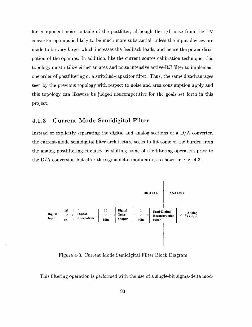
for component noise outside of the postfilter, although the 1/f noise from the I-V
converter opamps is likely to be much more substantial unless the input devices are
made to be very large, which increases the feedback loads, and hence the power dissi-
pation of the opamps. In addition, like the current source calibration technique, this
topology must utilize either an area and noise intensive active-RC filter to implement
one order of postfiltering or a switched-capacitor filter. Thus, the same disadvantages
seen by the previous topology with respect to noise and area consumption apply and
this topology can likewise be judged noncompetitive for the goals set forth in this
project.
4.1.3 Current Mode Semidigital Filter
Instead of explicitly separating the digital and analog sections of a D/A converter,
the current-mode semidigital filter architecture seeks to lift some of the burden from
the analog postfiltering circuitry by shifting some of the filtering operation prior to
the D/A conversion but after the sigma-delta modulator, as shown in Fig. 4-3.
DIGITAL ANALOG
16 16 Digital 1 Semi-Digital AnalogDigital , Digital Noise / Reconstruction OutputInput fn Interpolator Mfn Shaper Mfn Filter
Figure 4-3: Current Mode Semidigital Filter Block Diagram
This filtering operation is performed with the use of a single-bit sigma-delta mod-
93
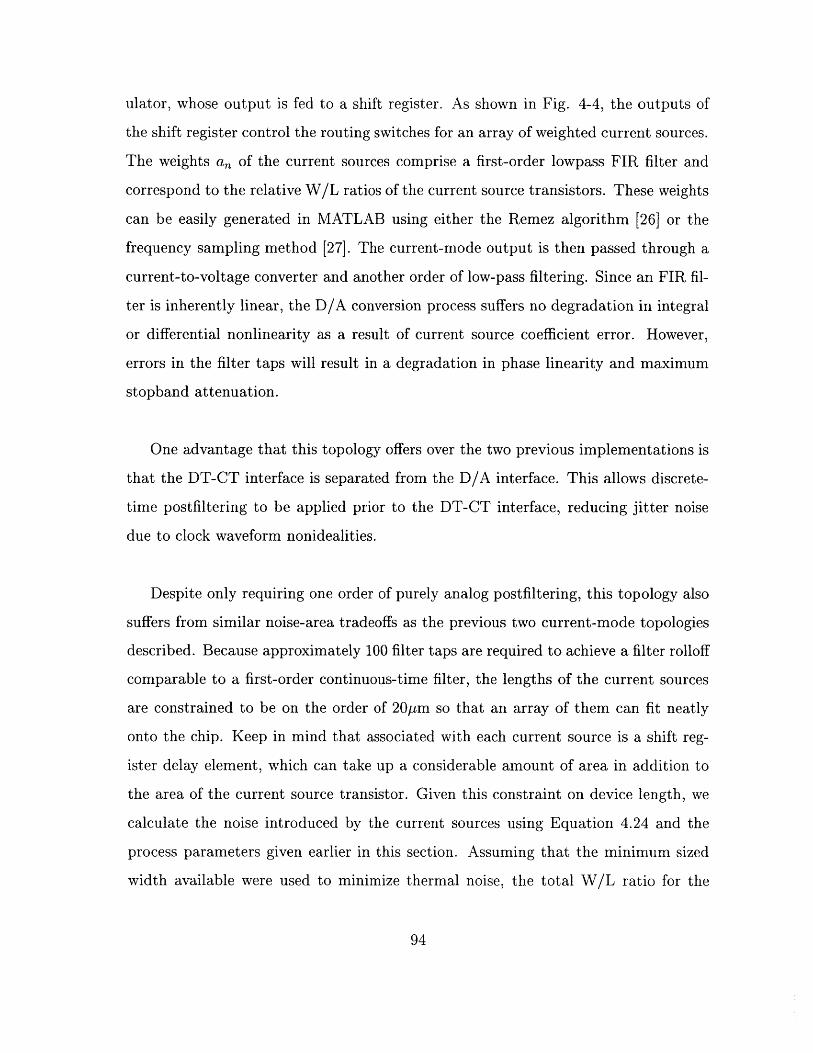
ulator, whose output is fed to a shift register. As shown in Fig. 4-4, the outputs of
the shift register control the routing switches for an array of weighted current sources.
The weights a, of the current sources comprise a first-order lowpass FIR filter and
correspond to the relative W/L ratios of the current source transistors. These weights
can be easily generated in MATLAB using either the Remez algorithm [26] or the
frequency sampling method [27]. The current-mode output is then passed through a
current-to-voltage converter and another order of low-pass filtering. Since an FIR fil-
ter is inherently linear, the D/A conversion process suffers no degradation in integral
or differential nonlinearity as a result of current source coefficient error. However,
errors in the filter taps will result in a degradation in phase linearity and maximum
stopband attenuation.
One advantage that this topology offers over the two previous implementations is
that the DT-CT interface is separated from the D/A interface. This allows discrete-
time postfiltering to be applied prior to the DT-CT interface, reducing jitter noise
due to clock waveform nonidealities.
Despite only requiring one order of purely analog postfiltering, this topology also
suffers from similar noise-area tradeoffs as the previous two current-mode topologies
described. Because approximately 100 filter taps are required to achieve a filter rolloff
comparable to a first-order continuous-time filter, the lengths of the current sources
are constrained to be on the order of 2 0 pm so that an array of them can fit neatly
onto the chip. Keep in mind that associated with each current source is a shift reg-
ister delay element, which can take up a considerable amount of area in addition to
the area of the current source transistor. Given this constraint on device length, we
calculate the noise introduced by the current sources using Equation 4.24 and the
process parameters given earlier in this section. Assuming that the minimum sized
width available were used to minimize thermal noise, the total W/L ratio for the
94
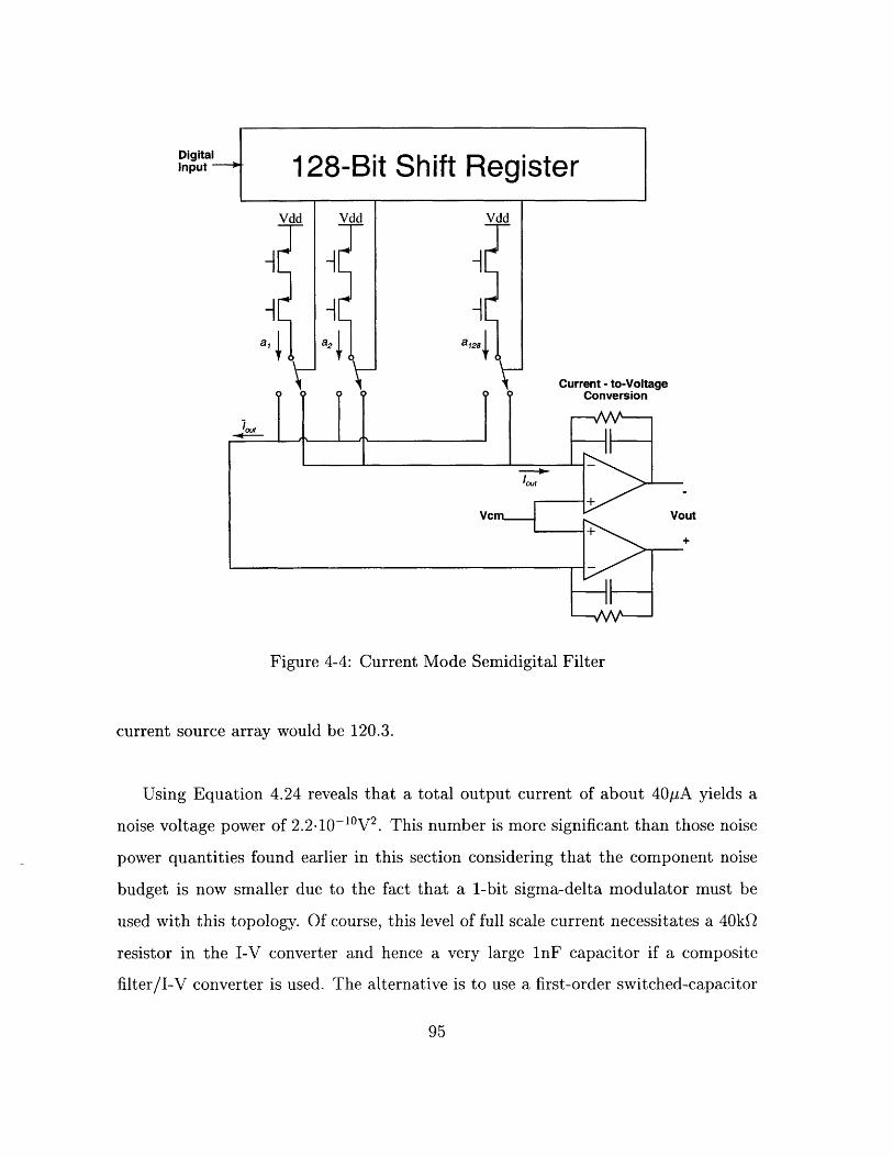
128-Bit Shift Register
Vdd Vdd
a, a. a2,
Vdd
Current - to-Voltage" Conversion
on vou
Figure 4-4: Current Mode Semidigital Filter
current source array would be 120.3.
Using Equation 4.24 reveals that a total output current of about 40PA yields a
noise voltage power of 2.2-10- 10V2 . This number is more significant than those noise
power quantities found earlier in this section considering that the component noise
budget is now smaller due to the fact that a 1-bit sigma-delta modulator must be
used with this topology. Of course, this level of full scale current necessitates a 40kQ
resistor in the I-V converter and hence a very large lnF capacitor if a composite
filter/I-V converter is used. The alternative is to use a first-order switched-capacitor
95
DigitalInput
VC
filter as a postfilter, but this will also consume a good amount of power and area in
addition to the area already consumed by the layout of the current source array.
4.2 Switched-Capacitor D/A and Postfilter Topolo-
gies
Switched-capacitor D/A converters function on the principle of charge distribution.
In general, a switched-capacitor D/A converter consists of a bank of weighted or unit-
sized capacitors that sample one of two reference voltages then integrate the resultant
net charge onto an opamp feedback capacitor. One advantage of switched-capacitor
D/As is that switched-capacitor network theory is well-developed and many of its
concepts are directly applicable to switched-capacitor D/A converters. Another key
selling point is that a switched-capacitor D/A converter can be integrated easily into
a switched-capacitor postfilter by breaking up the input capacitor into a bank of
weighted or unit-sized capacitors. Thus, no special conversion is required to interface
the DAC to the postfilter, as proved to be a constraint in the current-mode topologies.
If this is the case, then postfiltering can be performed before the DT-CT interface,
removing the out-of-band quantization noise that can increase the effect of clock jitter.
Although switched-capacitor topologies face a tradeoff between noise, power, and
area due to the kT/C noise relation [12], it can be shown that this tradeoff is not
as severe as those described for monolithic current-mode converters. In addition,
switched-capacitor techniques exist to reduce or nullify other sources of component
noise. For example, the correlated double sampling technique[28] can eliminate the
input-referred 1/f opamp noise in a switched-capacitor setup.
Interestingly, it can be noted that, in general, switched capacitor noise is pro-
portional to 4kTfo [29] Also, if the power dissipated in the opamps in the switched-Cf. i h oe isptdi h pmsi h wthd
96
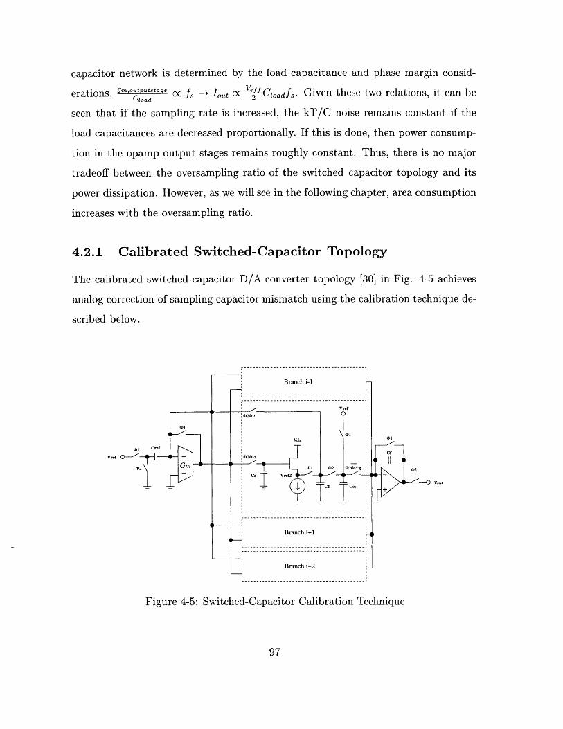
capacitor network is determined by the load capacitance and phase margin consid-
erationsgm,outputstage c f - Ic eff Cloadfs. Given these two relations, it can be
seen that if the sampling rate is increased, the kT/C noise remains constant if the
load capacitances are decreased proportionally. If this is done, then power consump-
tion in the opamp output stages remains roughly constant. Thus, there is no major
tradeoff between the oversampling ratio of the switched capacitor topology and its
power dissipation. However, as we will see in the following chapter, area consumption
increases with the oversampling ratio.
4.2.1 Calibrated Switched-Capacitor Topology
The calibrated switched-capacitor D/A converter topology [30] in Fig. 4-5 achieves
analog correction of sampling capacitor mismatch using the calibration technique de-
scribed below.
01
var 0---0
.2
Branch i-1
Vref
02-D
01Vdd
Cref
Gm 1 20
+ CiIcfi Ir. ca
Branch i+1
Branch i+2
Figure 4-5: Switched- Capacitor Calibration Technique
02
97
Each branch i of the D/A converter contains a coarse input capacitor Ci, which
can deliver a charge CciVref into the feedback capacitor, and a fine input capacitor CfP,
which can deliver a charge CfiVrefi, where Vrefi is an adjustable DC voltage. During
the reset phase hi., all input capacitors are charged to their reference voltages: Cci
to Vef and Cfi to Vrefi. Next, during the conversion phase (12, both capacitors Ci
and Cfi are discharged into Cf if xi=1, signaling that the cell is selected for output
by the thermometer-encoded DAC output.
To correct for the mismatch between the input capacitors, the calibration stage
shown above in Fig. 4-5 is connected to each of the unit elements one at a time, read-
justing each reference voltage Vrefi once per calibration cycle such that the combined
charges stored in Ci and Cfi iterate ever closer to CrefVref. To replace the branch
being calibrated at any given time while maintaining full input range, an additional
output unit above the number needed to converter the output of the thermometer-
encoder also needs to be added to the DAC array.
While the calibration routine of this topology avoids the need for large amounts of
digital dynamic element matching circuitry, it adds another static-power consuming
amplifier (in this case, a transconductor) to the overall topology in addition to requir-
ing one current source per cell, potentially dissipating a significant amount of power
for a 4 or 5-bit sigma-delta modulator. Also, this topology is subject to mismatched
charge injection error from the switches used in the calibration process. It can be
shown, however, [30] that errors due to switch mismatch will be at least 90dB below
the input signal level for reasonable process parameters.
Further modifications to this topology may also be implemented, including adding
correlated double-sampling techniques to correct 1/f noise, offset, and finite opamp
gain nonidealities. Switched-capacitor filtering circuitry may also be added to the
98
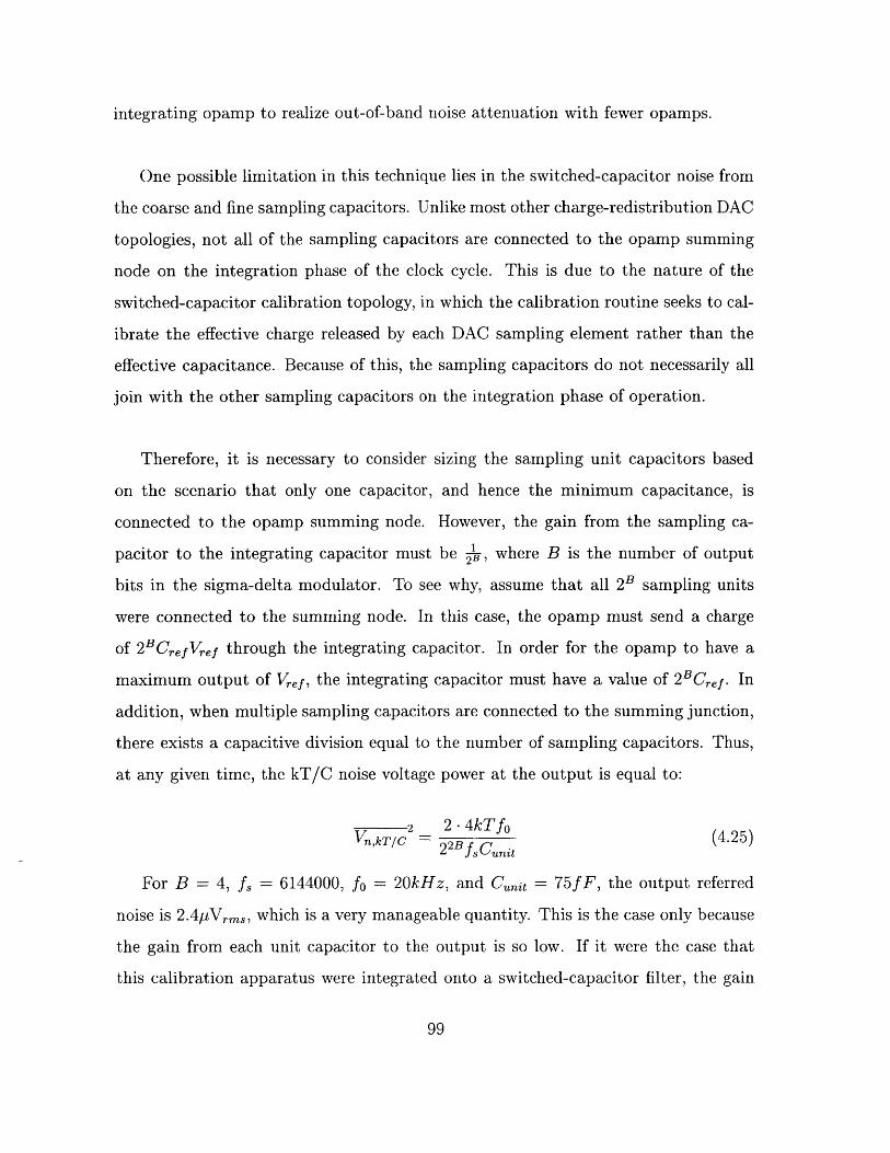
integrating opamp to realize out-of-band noise attenuation with fewer opamps.
One possible limitation in this technique lies in the switched-capacitor noise from
the coarse and fine sampling capacitors. Unlike most other charge-redistribution DAC
topologies, not all of the sampling capacitors are connected to the opamp summing
node on the integration phase of the clock cycle. This is due to the nature of the
switched-capacitor calibration topology, in which the calibration routine seeks to cal-
ibrate the effective charge released by each DAC sampling element rather than the
effective capacitance. Because of this, the sampling capacitors do not necessarily all
join with the other sampling capacitors on the integration phase of operation.
Therefore, it is necessary to consider sizing the sampling unit capacitors based
on the scenario that only one capacitor, and hence the minimum capacitance, is
connected to the opamp summing node. However, the gain from the sampling ca-
pacitor to the integrating capacitor must be L, where B is the number of output
bits in the sigma-delta modulator. To see why, assume that all 2B sampling units
were connected to the summing node. In this case, the opamp must send a charge
of 2BCrefVref through the integrating capacitor. In order for the opamp to have a
maximum output of Vref, the integrating capacitor must have a value of 2BCref. In
addition, when multiple sampling capacitors are connected to the summing junction,
there exists a capacitive division equal to the number of sampling capacitors. Thus,
at any given time, the kT/C noise voltage power at the output is equal to:
2 2 -4kTfoVn,kT/c = 22Bf Ct (4.25)
2fsCunit
For B = 4, f, = 6144000, fo = 20kHz, and Cuni = 75fF, the output referred
noise is 2.4Vrms, which is a very manageable quantity. This is the case only because
the gain from each unit capacitor to the output is so low. If it were the case that
this calibration apparatus were integrated onto a switched-capacitor filter, the gain
99
seen to the output would be one or greater, necessitating a greater unit capacitor size.
Although kT/C noise seems to impose little constraint on the sampling capacitor
size, fixed charge error from the switches in the calibration routine will. For example,
the holding capacitor Ci must hold an amount of charge equal to Ci(Vrefi + Vthresh)
in order for unit element i to be perfectly calibrated, where Vrei is assumed to
be the voltage required to be placed on Cfi in order to offset the charge error
CrefVref - CciVref.
As in the current-calibrated case, the charge held on this capacitor is subject to
nonidealities [21]. First, leakage current present at the parasitic diode at the drain of
the switch connecting to the capacitor causes the voltage Vefi to drop. In addition,
mismatch in the clock feedthrough of the switch alters Vrefi and degrades the linearity
of the converter. The magnitude of these errors can be reduced by making Ci (the
calibration charge holding capacitor) larger and by decreasing the ratio of Cfi/Cci.
In order to maintain the SNDR of the D/A converter to an effective resolution of
N bits, it is desirable to retain N + 2 bits of linearity in each unit element to leave
a considerable budget for the component noise that will be introduced in any analog
postfiltering that is done. This means that for N = 16, all output charges must be
accurate to (3.8 - 10 6 )CrefVref.
Choosing D/A converter capacitances as: Cf = 75fF, which is the minimum
sized capacitor, Cef = 250fF Cci = 0.95-, Cef, and Ci = 0.35pF.
Also, the switch to Ci is chosen to be minimum sized, that is, W = 0.5[tm, L =
0. 2 5pm, with a process-dependent diffusion length of Ldiff = lpm, and assuming the
maximum overdrive voltage on the switch is about 0.5V, we can write:
100
Ileak ~ O.OlWswitehLdiff
CoxWwitchLswitchVef5s e - charge mismatch (4.27)10
where charge mismatch between switches is on the order of 10%.
AVref,q =Aqch (4.28)ci
AVref,leak = At (4.29)ciwhere At is the time in between calibration refreshes for each unit element. For
B = 4 and a calibration time per element of 0.2ps, At = 3.21p-s, and the relative
maximum charge error is therefore:
Cf (AVrefq +AVref,leak) = 3.43 - 10-6 (4.30)Cre! Vrej
for Vref = V.
Although the unit fine sampling capacitors can be minimum sized, the fact that
they have to be a certain fraction of the coarse sampling capacitors means that the
integrating opamp has to drive a peak total capacitance of 5.2pF in addition to the
load of the switched-capacitor biquad filter. In addition, the total capacitance re-
quired by a differential implementation is 26.8pF, a substantial number given that
the mismatch calculations above were generous. This total capacitance was calculated
assuming that the size of the integrating capacitor is sized such that the integrating
voltage gain is 2 to achieve the required voltage swing. Considering that this D/A
converter block already consumes a large amount of static power to drive the 5.2pF
capacitance and 26.8pF of capacitance die area before even performing any postfilter-
ing suggests that this topology will not be power and area competitive with topologies
101
(4.26)
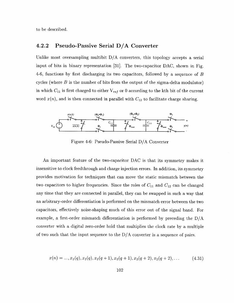
to be described.
4.2.2 Pseudo-Passive Serial D/A Converter
Unlike most oversampling multibit D/A converters, this topology accepts a serial
input of bits in binary representation [31]. The two-capacitor DAC, shown in Fig.
4-6, functions by first discharging its two capacitors, followed by a sequence of B
cycles (where B is the number of bits from the output of the sigma-delta modulator)
in which C11 is first charged to either Vref or 0 according to the kth bit of the current
word x(n), and is then connected in parallel with C12 to facilitate charge sharing.
x(n,k) (O * 1) (DbD2) (2
Cf I C22V,.f x(-n,k) (D 4rst)m q2 y(n)
Figure 4-6: Pseudo-Passive Serial D/A Converter
An important feature of the two-capacitor DAC is that its symmetry makes it
insensitive to clock feedthrough and charge injection errors. In addition, its symmetry
provides motivation for techniques that can move the static mismatch between the
two capacitors to higher frequencies. Since the roles of C11 and C12 can be changed
any time that they are connected in parallel, they can be swapped in such a way that
an arbitrary-order differentiation is performed on the mismatch error between the two
capacitors, effectively noise-shaping much of this error out of the signal band. For
example, a first-order mismatch differentiation is performed by preceding the D/A
converter with a digital zero-order hold that multiplies the clock rate by a multiple
of two such that the input sequence to the D/A converter is a sequence of pairs.
x(n) = ...,x 2 (q),X 2 (q),X 2 (q +1), X 2 (q + 1), x 2 (q + 2), 2 (q + 2),... (4.31)
102
It follows that since C11 and C12 are interchanged in the two conversions of each
value x2 (n2), the error signal will be of the form:
e(n) = ..., eq, -eq, eq+1, -eq+1, eq+2, -eq+2, ... (4.32)
which can be interpreted as the first-order difference of:
e*(n) = ..., eq, 0, eq+1, 0, eq+2, 0, ... (4.33)
Since a first-order difference has a high-pass characteristic, we can argue that the
mismatch error has been shaped to high-frequency noise by this operation.
An interesting side note is that because the individual DACs can be made to
occupy little area, they can be used as elements in an analog FIR filter of moderate
length (2-10 taps) to avoid the hardware penalty of a brute-force switched-capacitor
filter when suppressing out-of-band noise as shown in Fig. 4-7. Note that since all
of the weighted filter capacitors a1C1 - aC 1 are in parallel on the integrating phase
of operation, it is the total filter capacitance that should be taken into account when
determining the filter kT/C noise.
The reconstruction filter described above never sees the filter capacitors a1 C1 -
anC1 as a load in the feedback position. Therefore, the filter opamp does not have
to drive the FIR sampling capacitance, relaxing the opamp drive requirements. The
overall discrete-time transfer function of this reconstruction filter is:
(a, + a2 z--1 + ...) (4.34)V 1) + Cf - fZ-1
CDAC CDAC
CDAC =(aC + a2C 1 + .... anC) (4.35)
103
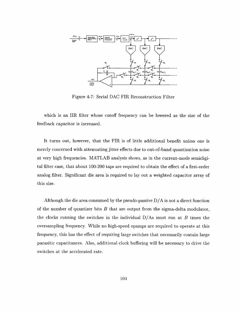
DAC DAC DAC
1 imI
Figure 4-7: Serial DAC FIR Reconstruction Filter
which is an IIR filter whose cutoff frequency can be lowered as the size of the
feedback capacitor is increased.
It turns out, however, that the FIR is of little additional benefit unless one is
merely concerned with attenuating jitter effects due to out-of-band quantization noise
at very high frequencies. MATLAB analysis shows, as in the current-mode semidigi-
tal filter case, that about 100-200 taps are required to obtain the effect of a first-order
analog filter. Significant die area is required to lay out a weighted capacitor array of
this size.
Although the die area consumed by the pseudo-passive D/A is not a direct function
of the number of quantizer bits B that are output from the sigma-delta modulator,
the clocks running the switches in the individual D/As must run at B times the
oversampling frequency. While no high-speed opamps are required to operate at this
frequency, this has the effect of requiring large switches that necessarily contain large
parasitic capacitances. Also, additional clock buffering will be necessary to drive the
switches at the accelerated rate.
104
The lowest achievable OSR in this topology is determined by the fact that the
sampling clock has a worst-case jitter performance of oj i Ins. In order to guaran-
tee that jitter noise at the DT-CT interface is below 96dB, the oversampling ratio
must be kept no less than 64, as predicted by the jitter equation given in the follow-
ing section. Since the second-order mismatch shaping described in [31] requires an
oversampling ratio that is a multiple of three, an oversampling ratio of 72 will be used.
According to Steensgaard, et al. [31], for an OSR of 72 and for a capacitor mis-
match error of 6 = 0.1%, first order mismatch shaping achieves an SNDR of -85dB,
much too high to obtain the required 16 bit resolution. Second order mismatch shap-
ing achieves an SNDR of -130dB for this same level of mismatch. Assuming that, for
an increase in 6 by a factor K, the SNDR of the mismatch-shaping scheme degrades
by 20 loglo(K)dB, a capacitor mismatch of 1% will result in an SNDR of -110dB.
This resolution is sufficient to guarantee that the shaped mismatch error is negligible
compared to the component noise.
For commercial design purposes, the factor 6 is equal to the value 6- to account
for process variation across a large batch. The value of - is therefore 0.16%, which
corresponds to a capacitance of 0.204pF in the process available for this project.
It turns out that noise requirements set the final capacitor size. Assuming that,
since a large FIR is infeasible, only one switched-capacitor DAC will be used prior
to the IIR lowpass filter. Since both capacitors of the two-capacitor D/A converter
are seen in parallel at the output during their sampling into the analog IIR filter, the
kT/C noise is dependent on the sum of their values. Thus, the output referred kT/C
noise is given by:
105
4kTf o 4k -300 . 20000 (lop ms) 2
nkT/C CfS - C - 3456000
Where OPVrms of total component noise has been budgeted to the D/A converter
capacitance, leading to a capacitance of 0.5pF for each of the twin capacitors.
As the switches to these capacitors are responsible for carrying and holding the
signal voltages, the design is constrained to use CMOS switches to avoid threshold
voltage errors in the signal path. For an oversampling ratio of 72, a B=5 bit sigma-
delta modulator is required to remove all sigma delta quantization noise from the
signal band. For this setup, the internal switches inside the pseudopassive D/A con-
verter must operate at fa = (N + 1)fs = 20.736MHz in order to handle the incoming
serial bitstream.
Good design practice calls for switches to be sized such that their time constants,
in conjunction with their load capacitances have sufficient linear settling accuracy.
For settling accuracy to 0.01%, the RC time constant formed by the switches should
be about 1/7th of the sampling period, that is, 2RC 7f3. Thus, to drive the
combined load capacitance, as the switches need to do in the worst-case scenario, the
resistance required is 548Q. Noting that two switches are in series, and noting that
the resistance of a CMOS switch can be approximated as [32]:
2VddRswitenx kn(Vdd - Vth,n) 2 + k (Vdd - Vth,p (3
Resulting in the values:
Wn = 1.5pm, W, = 7.12pm
106
assuming that, for the switches, kp = ka, W, =- C-"W.
The problem with switches such as these is that they have nonlinear parasitic
capacitances that are significant in size compared to the charge storage capacitors.
Since the drain- and source-to-bulk capacitances of the switches appear in parallel
with the capacitors of the two-capacitor D/A converter, they can effectively create
a sampling capacitor which is nonlinear with the applied voltage. To quantify the
effects of these nonlinear capacitors, it is necessary to first calculate their values.
From the process handbook,
F F_
Cn = 1.8366- 10-3 F2, Cj, = 1.8339. 10-3 F
Ciswn = 4.235. 10-F -, Cj, = 3.473 - 10-10 -m mn
Ldiff = 1pm, mj = 0.5, 1 B = 0-9, Vbulk,n = OV, bulk,p = 2.5V
Noting that:
Cdbn - Csbn (Cin *W,- Ldiff) + (Cjswn - (Wn + 2Ldff)) (4.38- ( Vkd)mi
Cdbn = sbn =0.00344pF (4.39)Cabs= Con (1+ Vd)0-5 (.9
b -0.0154pFCdb, = Cab, - (3.78 - )0.5 (4.40)
\0.9/
From the two-capacitor D/A converter schematic, one can readily see that each
capacitor sees at least two CMOS switches at any given time, in addition to one other
107
NMOS switch which will be neglected for the purposes of this discussion.
It is also important to note that Vd,max = Vef = 2V and that Vd,min = OV
Inserting these numbers into the above equations reveals that
For Vd,max, the total parasitic capacitance seen by each capacitor equals: 0.02852pF.
For Vd,min, the total parasitic capacitance seen by each capacitor equals: 0.02272pF.
For a nominal worst-case capacitor value of 0.5pF (when the two capacitors are
not in parallel), the parasitic capacitance variation described above results in a total
capacitance variation of 1.02% over the specified voltage range. Although mismatch
shaping can correct mismatches between capacitors, it is shown that mismatches
between a single capacitor at different voltages can invalidate the first-order noise
shaping process described by Steensgaard, et al.
We know from the Steensgaard paper that the error signal for a particular con-
version is of the form:
e(n) = 6 -Vref -F[x(n, k)] (4.41)
where x(n, k) is the incoming serial sequence of bits, n is the current signal sym-
bol, k is the current symbol bit, and F is a function that relates the bits of the current
signal symbol the the error resulting from the two-capacitor D/A switching opera-
tion. The error shaping techniques described in Steensgaard, et al. rely on the fact
that each input symbol n produces a distinct e(n) and that -e(n) can be generated
merely by switching C11 and C 22.
108
Introducing the mismatch term
6 =C1 - C12 (4.42)C11 + C12
Swapping C12 and C1 yields
6 new = C12 - C1 = old (4.43)C11 + C2
Therefore,
e(n)new = 6new -Ve- F [x(n, k)] (4.44)
- 6 old -Vref - F[x(n, k)] (4.45)
- -e(n)old (4.46)
However, if
C11 = C,nominat + Cnl,parasitic(Vin) (4.47)
C12 C12,nominal + C12,parasitic(Vhold) (4.48)
where Vin represents a voltage in the sequence Vref - x(n, k), depending on the
input bit, and where VoId is the voltage seen by the signal holding capacitor, which
can be denoted as v(n, k - 1).
With parasitics, the error is still a function of the particular input word, but the
capacitor mismatch factor 6 becomes:
6-- CI(Vin) - C12(Vold)
C1I(Vin) + C12(Vold)
and 6 is thus a function of x(n, k).
109
Note that because of the newly significant voltage dependency of the two capaci-
tors, switching their positions in the circuit no longer has the effect of maintaining the
magnitude of 6 constant. After switching positions, C 1 2 will see the voltages Vn,(n,k)
and C11 will see the voltages Vh,,d,(n,k). Mathematically, if 6new = -6,rs, then
6new - C12(Vhold) - C11 (Vin) (4.50)C11(Vin) + C12(Vhold)
However, since C12 now sees Vi and C11 sees Vnt,
C12(Vin) - Cn(Vhold)
new C(Vin)+ C12(Vhold)
which is only equal to - 6old if Vin = Vold for the entire conversion operation of
symbol n. To numerically examine the potential magnitude of such an error, consider
the following example. If for the input symbol x(n, k), the first k - 1 bits are equal
to zero while the final bit k is equal to 1, the voltage Vold will be zero until the final
cycle of the serial DAC operation. Until this time, the effect of any mismatch between
the two capacitors is zero, since they have been sharing zero charge on every cycle.
On the final stage, however, Vin = Vej = 2V and Vho0 d = OV prior to conversion.
In this case,
Cii,nominai = 0.5025pF (hereafter abbreviated C1 1,nand C12,n)
C12,nominal = 0.4975pF(so that Jnominal = 1%)
Cii,parasitic(Vref) = C12,parasitic(Vref) = 0.02852pF
Cn1 ,parasitic(Vhold) C12,parasitic(VoId) = 0.02272pF
110
Cn(Vin) - C12(Vold)
ICnI(Vin) + C12(Vhold)
Clln - C12n + C11 (Vin) - C12(Vhold) Clln + C12n
CnOn + C12n + C1n(Vin) + C12p(VhoId) Cin - C1n-minal (4.53)
( + C11p(Vi. )-C 2 p(Vhold)
6 C 6 nominat _ _ _-C12 (4.54)
+ C1p(Vin)+C1 2 p(Vhld)C1In+C12.
Since the second term in the denominator is very small, it can be neglected
6 = 6 nominal 1 + Cl(in) C12p(Vhold)(4.55)Cn- C12n
Plugging in values yields:
6 = 6 nominal - 2.156
Switching the positions of the two capacitors yields
6 = 6 nominal 1 + C12p(Vin) - Cllp(Vhold) (4.56)C12n - C11n
6 = Jnominal ' (-0.156)
The two values 6 do not cancel out when the two capacitors switch positions, thus
invalidating any mismatch correction that could make this D/A topology feasible.
Note that this problem is roughly independent on the size of the nominal capacitor
used and worsens with increasing sampling frequency, in which case larger switches
relative to the size of the capacitors are required.
111
4.2.3 Switched-Capacitor with Dynamic Element Matching
and Direct Charge Transfer
As stated before, one disadvantage of switched-capacitor D/A topologies is the un-
desirable tradeoff between kT/C noise, capacitor area, and power dissipation. One
circuit method that decouples the power dissipation factor from this tradeoff is known
by several names, but for the purposes of this discussion will be referred to as Direct
Charge Transfer [17]. Shown in Fig. 4-8, the Direct Charge Transfer (hereafter re-
ferred to as DCT) technique realizes a first-order filter transfer function while never
connecting its sampling capacitance in a configuration in which the opamp sees the
capacitance as a load through the feedback network. That is, unlike traditional RC-
equivalent switched-capacitor networks in which the opamp supplies the charging cur-
rent for the integrating capacitor, the sampling capacitance CDAC connects in parallel
with the integrating capacitance Chd, passively sharing the input charge. The opamp
is now only required to drive the bottom-plate capacitance of the feedback capacitor,
which is negligible in many modern wafer processes that offer metal-insulator-metal
capacitors. Since this input capacitance often forms the dominant load capacitance of
traditional switched-capacitor implementations, this technique can save a substantial
amount of power.
Although originally conceived as a method to introduce crosstalk between signal
branches [34] and later used as a buffer [35] and finally a high-frequency quantization
noise reject filter [33], DCT has the potential to fill the role of the primary analog
postfilter in a monolithic D/A converter. It can be shown that the transfer func-
tion of the system shown in Fig. 4-9, in which a switched-capacitor D/A converter
employing Dynamic Element Matching is integrated onto a second-order postfilter
employing two DCT blocks, is given as:
112
Chold
CDAC
Vref
OUT
Figure 4-8: Direct-Charge Transfer Concept
H(z) = Z2(4.57)1+ CFB _ CFB . -- 1)2
CDAC CDAC
As will be shown in Chapter 5, the required ratio of CFB to CDAC for an over-
sampling ratio of 128 is 25.
It has already been stated that a four-bit dynamic element matching scheme can
remove almost all quantization noise from the signal band. Thus, for a minimum
capacitor size of 75fF, the input capacitor array will consume 1.2pF of capacitance.
This results in an output-referred component noise power contribution of 9 -10- 1 1 V2 .
It turns out that there is enough room in the quantization noise budget to make the
input capacitors to the second stage 0.3pF each, contributing a component noise power
of 3.6 -10- 10V 2 . For a differential implementation, the total approximate capacitance
of this topology is 78pF while only 0.3pF of capacitance needs to be driven, along with
the lumped capacitance seen at the output of the switched capacitor filter. These
numbers, which will be explained in greater detail later, show that the topology
described above will trump all others for the low-power, low-area monolithic solution.
113
Switced-Capacitor DACitegrnto the otoN fitn
vref )
gnd
vref -- )H
Sum Phase 1 ($1)
-n .. Q-. Phase 2 (02)
Thermometer - EncodedDigital Input SO to S 15
X16 Out+
Capacior ay sev + Out+
Aadke MRdf.d
Capacitor Array sam-
Om-
Figure 4-9: Four-bit SC D/A Converter with DCT Postfiter
4.3 Dynamic Element Matching Techniques
Although a D/A converter may have static errors resulting from mismatch between
its unit elements, it is possible to select these elements in such a way as to convert
these DC errors into a pseudo-random wideband noise signal [133 that can be par-
tially removed by the analog reconstruction filter. The general class of such strategies
known as dynamic element matching accomplishes this by choosing different elements
to represent a digital input code at different times. This technique especially suits
oversampling converters because, as with quantization noise, this mismatch noise
power is spread over the signal bandwidth, and less noise falls in the signal band as
the oversampling ratio is increased [13]. One caveat to these techniques is that the
element selection process is governed by digital control circuitry which must be im-
114
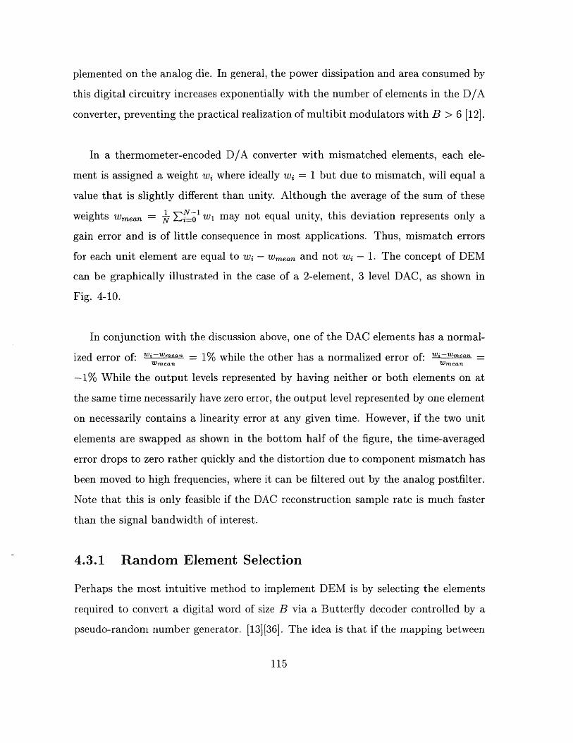
plemented on the analog die. In general, the power dissipation and area consumed by
this digital circuitry increases exponentially with the number of elements in the D/A
converter, preventing the practical realization of multibit modulators with B > 6 [12].
In a thermometer-encoded D/A converter with mismatched elements, each ele-
ment is assigned a weight wi where ideally wi = 1 but due to mismatch, will equal a
value that is slightly different than unity. Although the average of the sum of these
weights Wmean = A Z 1 W, may not equal unity, this deviation represents only a
gain error and is of little consequence in most applications. Thus, mismatch errors
for each unit element are equal to Wi - Wmean and not wi - 1. The concept of DEM
can be graphically illustrated in the case of a 2-element, 3 level DAC, as shown in
Fig. 4-10.
In conjunction with the discussion above, one of the DAC elements has a normal-
ized error of: Wi-Wmean = 1% while the other has a normalized error of: wiWmean-Wmean Wmean
-1% While the output levels represented by having neither or both elements on at
the same time necessarily have zero error, the output level represented by one element
on necessarily contains a linearity error at any given time. However, if the two unit
elements are swapped as shown in the bottom half of the figure, the time-averaged
error drops to zero rather quickly and the distortion due to component mismatch has
been moved to high frequencies, where it can be filtered out by the analog postfilter.
Note that this is only feasible if the DAC reconstruction sample rate is much faster
than the signal bandwidth of interest.
4.3.1 Random Element Selection
Perhaps the most intuitive method to implement DEM is by selecting the elements
required to convert a digital word of size B via a Butterfly decoder controlled by a
pseudo-random number generator. [13][36]. The idea is that if the mapping between
115
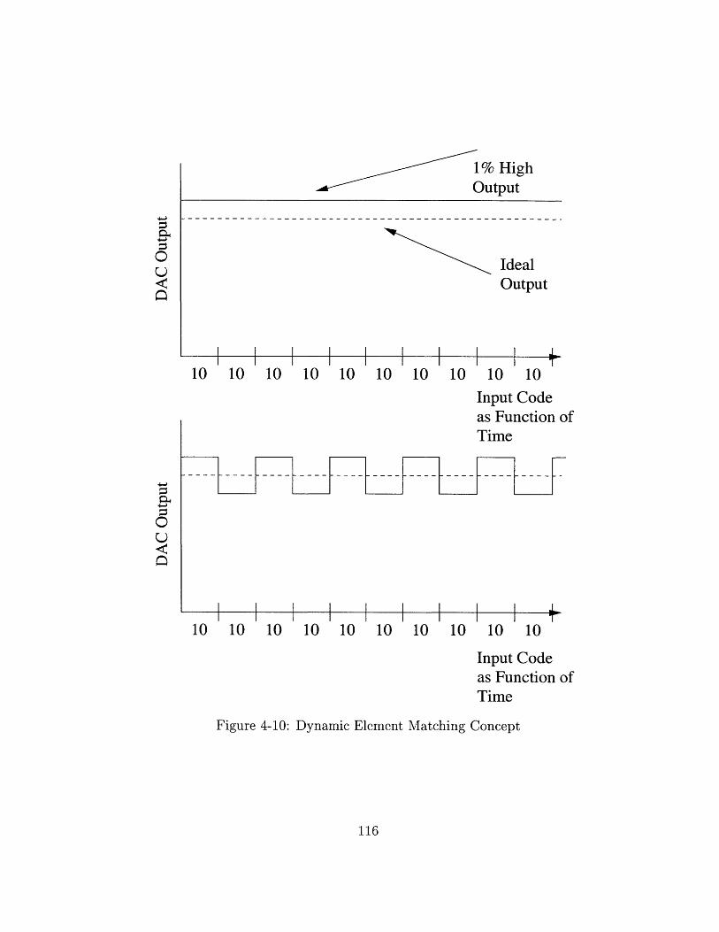
1% Highoutput
IdealOutput
10 10 10 10 10 10 10 10 10 10Input Codeas Function ofTime
10 10 10 10 10 10 10 10 10 10
Input Codeas Function ofTime
Figure 4-10: Dynamic Element Matching Concept
116
the thermometer encoded sigma-delta modulator output bits and the D/A converter
elements are determined at random for every sample time, there will be no correlation
between the total mismatch error between sample times, resulting in the mismatch
error having white noise signal statistics.
Assuming that the sigma-delta modulator is oversampled with OSR=M, the pseu-
dorandom mismatch noise will be spread uniformly across all frequencies, and only
1/M of the total mismatch noise power will fall in the signal band. Given that there
are N levels in the thermometer encoded sigma-delta modulator output, the output
signal swing has a maximum excursion from 0 to N. Given these parameters, it can
be shown [36] that the maximum SNR attainable by this scheme is equivalent to:
NM
SNR = (4.58)
Where o-, is the standard deviation of the mismatch between unit elements. Good
design practice calls for the 6a mismatch deviation given in the process handbook to
be used for this value in order to guarantee acceptable process yield. As seen from
the formula above, each doubling of the oversampling ratio yields an additional 3dB
of signal to noise ratio.
4.3.2 Data Weighted Averaging
While this sort of linearity improvement is certainly better than leaving static errors
in the D/A converter, it is generally not sufficient to realize a high performance im-
plementation. The Data Weighted Averaging algorithm (DWA) potentially achieves
a resolution benefit of 9dB per decade of oversampling without the addition of com-
plicated digital control circuitry [22].
The DWA algorithm is performed by sequentially selecting elements for use from
117
the D/A array, beginning with the next available element, as shown in Fig. 4-11.
Active Multibit DAC Elements Time
Input 0 1 2 3 4 5 6 7 8 9 10 11 12 13 14 15Data
2
9
10
5
6
8
Figure 4-11: Conceptual Operation of DWA Algorithm
As can be seen in Fig.4-11, the DWA algorithm guarantees that each DAC element
is used the same number of times and that all of the DAC elements are utilized at the
maximum possible rate. [22]. Since it only takes a few cycles of operation before all
of the DAC elements are used, their individual errors Wi - Wmean quickly sum to zero.
This implies that mismatch-induced distortion is moved to very high frequencies [22].
It can be demonstrated through hand analysis that the DWA algorithm in fact
shapes the resulting mismatch error much as a first-order noise shaper [36] and that
for a random input signal, the achievable resolution is approximately equal to:
resolution = log 2 (1jM (bits) (4.59)7rao (I - N-)
where M = OSR, N = 2 B, and or equals the 6a process variation of the DAC
unit elements [36]. In addition, MATLAB simulation shows that the DFT of the mis-
match error noise from the DWA algorithm rises approximately as first-order shaped
noise, as shown in Fig. 4-12.
118
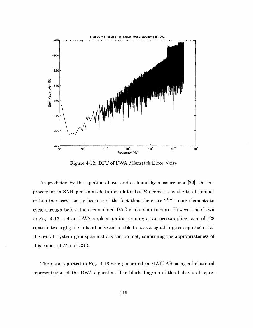
Shaped Mismatch Error "Noise" Generated by 4 Bit DWA-80
-100-
-120-
-140-
-160e
-180-
-200-
-220......IIII10 102 103 104 105 10 107
Frequency (Hz)
Figure 4-12: DFT of DWA Mismatch Error Noise
As predicted by the equation above, and as found by measurement [22], the im-
provement in SNR per sigma-delta modulator bit B decreases as the total number
of bits increases, partly because of the fact that there are 2B-1 more elements to
cycle through before the accumulated DAC errors sum to zero. However, as shown
in Fig. 4-13, a 4-bit DWA implementation running at an oversampling ratio of 128
contributes negligible in band noise and is able to pass a signal large enough such that
the overall system gain specifications can be met, confirming the appropriateness of
this choice of B and OSR.
The data reported in Fig. 4-13 were generated in MATLAB using a behavioral
representation of the DWA algorithm. The block diagram of this behavioral repre-
119
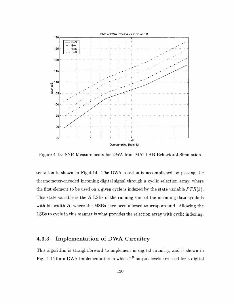
a
ziCC)
130
125
120
115
110
105-
100-
95-
90-
SNR of DWA Process vs. OSR and B
10 2Oversampling Ratio, M
Figure 4-13: SNR Measurements for DWA from MATLAB Behavioral Simulation
sentation is shown in Fig.4-14. The DWA rotation is accomplished by passing the
thermometer-encoded incoming digital signal through a cyclic selection array, where
the first element to be used on a given cycle is indexed by the state variable PTR(k).
This state variable is the B LSBs of the running sum of the incoming data symbols
with bit width B, where the MSBs have been allowed to wrap around. Allowing the
LSBs to cycle in this manner is what provides the selection array with cyclic indexing.
4.3.3 Implementation of DWA Circuitry
This algorithm is straightforward to implement in digital circuitry, and is shown in
Fig. 4-15 for a DWA implementation in which 2B output levels are used for a digital
120
-BB=3- B=4
- B=5 - ---B=6:
-.. .. -. ... -.. ...... -. ..-
-. .-. . -. . -
- ..... -.. .. -.. .. ...
- .... . -.. ... ..... ...................
-. .... -.. .. -.. ... -. . -.. .. -.. ........ -.. ..
-. . - ... -.. .................. -.. ....
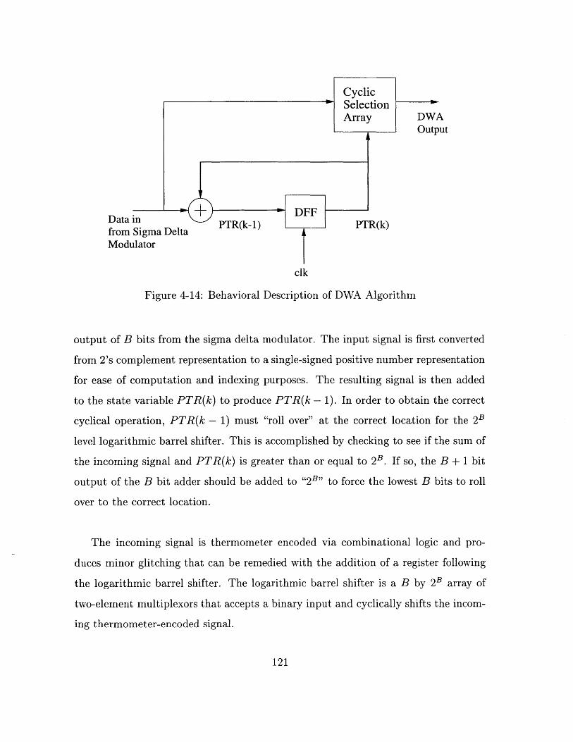
CyclicSelectionArray DWA
Output
Data in + DFF
from Sigma Delta PTR(k-1) PTR(k)
Modulator
clk
Figure 4-14: Behavioral Description of DWA Algorithm
output of B bits from the sigma delta modulator. The input signal is first converted
from 2's complement representation to a single-signed positive number representation
for ease of computation and indexing purposes. The resulting signal is then added
to the state variable PTR(k) to produce PTR(k - 1). In order to obtain the correct
cyclical operation, PTR(k - 1) must "roll over" at the correct location for the 2'
level logarithmic barrel shifter. This is accomplished by checking to see if the sum of
the incoming signal and PTR(k) is greater than or equal to 2B. If so, the B + 1 bit
output of the B bit adder should be added to "2B" to force the lowest B bits to roll
over to the correct location.
The incoming signal is thermometer encoded via combinational logic and pro-
duces minor glitching that can be remedied with the addition of a register following
the logarithmic barrel shifter. The logarithmic barrel shifter is a B by 2B array of
two-element multiplexors that accepts a binary input and cyclically shifts the incom-
ing thermometer-encoded signal.
121
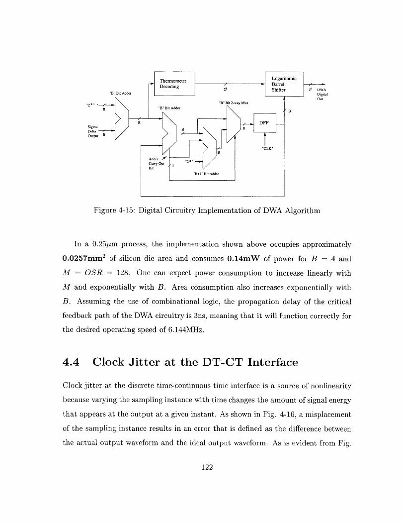
Thermometer Logarithmic
S Decoding -'* BarrelDecdin Shifter 2" DWA
"B" Bit Adder Delt"a
Biut
"2 - m "B" Bit 2-way Muxo p a pox t
B "B" Bit Adder c' B
BDIFF
Otput BB
"CLK"
Adder "Carry Out 2Bu_
Bit
"B+1" Bit Adder
Figure 4-15: Digital Circuitry Implementation of DWA Algorithm
In a 0.25pmn process, the implementation shown above occupies approximately
0.0257mm 2 of silicon die area and consumes 0.14mW of power for B = 4 and
M = OSR = 128. One can expect power consumption to increase linearly with
M and exponentially with B. Area consumption also increases exponentially with
B. Assuming the use of combinational logic, the propagation delay of the critical
feedback path of the DWA circuitry is 3ns, meaning that it will function correctly for
the desired operating speed of 6.144MHz.
4.4 Clock Jitter at the DT-CT Interface
Clock jitter at the discrete time-continuous time interface is a source of nonlinearity
because varying the sampling instance with time changes the amount of signal energy
that appears at the output at a given instant. As shown in Fig. 4-16, a misplacement
of the sampling instance results in an error that is defined as the difference between
the actual output waveform and the ideal output waveform. As is evident from Fig.
122
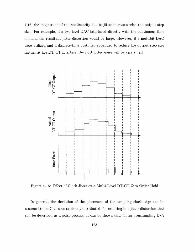
4-16, the magnitude of the nonlinearity due to jitter increases with the output step
size. For example, if a two-level DAC interfaced directly with the continuous-time
domain, the resultant jitter distortion would be large. However, if a multibit DAC
were utilized and a discrete-time postfilter appended to reduce the output step size
further at the DT-CT interface, the clock jitter noise will be very small.
I I I I I I I T
I II I I I I I I I
I I
Figure 4-16: Effect of Clock Jitter on a Multi-Level DT-CT Zero Order Hold
In general, the deviation of the placement of the sampling clock edge can be
assumed to be Gaussian randomly distributed [6], resulting in a jitter distortion that
can be described as a noise process. It can be shown that for an oversampling D/A
123

converter, the in-band jitter noise power at the output is given by [40]:
2(7rojAfo) 2 ~ ( f2] (.AT < -1 + ( (4.60)M A 2 fo
where P 2/A 2 is the ratio of out-of-band quantization noise power to signal power.
Since this result applies at the DT-CT interface, the value P is the amount of out
of band quantization noise after any discrete-time analog postfiltering (such as a
switched-capacitor postfilter or a semidigital current source filter).
It is known that the input clock supplied to this project has a worst case oj = 1nsA
2
and that the signal to noise ratio 2 should be on the order of 98dB to keep jitter
noise negligible. Also noting that MATLAB computations of P confirm that P << A
for the case of a multibit D/A converter followed by a second order discrete-time
postfilter, so
A2 M
10 logo 2 > 10 log 10 (4.61)Ny 1 4 (7ro ufo)2
We find that M=128 yields an approximate SNR of 99dB while M=64 yields an
approximate SNR of 96dB.
124
Chapter 5
Switched-Capacitor Postfiltering
Most on-chip filters, in addition to other circuits such as integrators, gain stages,
and comparators, are implemented using switched-capacitor techniques. Switched-
capacitor circuits move charge around a capacitive network based on an input clock
and hence are discrete-time blocks operating in the analog domain, resulting in an
explicit separation of the DT-CT and D/A interfaces. Thus, switched-capacitor cir-
cuits, and notably switched-capacitor filters, are typically analyzed using Z-domain
frequency response expressions. Careful application of the bilinear transform is es-
sential to relating capacitor ratios to pole frequencies in the continuous-time domain.
Although nominal values of integrated circuit components vary widely, in most
switched-capacitor filters key parameters such as gain and frequency response are set
by capacitor ratios, whose matching can be very accurate, with error on the order
of 0.1%. [3] Switched capacitor filters, in general, have good linearity and dynamic
range properties, and as has been discussed previously, reduce the effect of clock jitter
at the DT-CT interface.
125
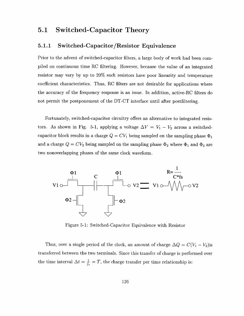
5.1 Switched-Capacitor Theory
5.1.1 Switched-Capacitor/Resistor Equivalence
Prior to the advent of switched-capacitor filters, a large body of work had been com-
piled on continuous time RC filtering. However, because the value of an integrated
resistor may vary by up to 20% such resistors have poor linearity and temperature
coefficient characteristics. Thus, RC filters are not desirable for applications where
the accuracy of the frequency response is an issue. In addition, active-RC filters do
not permit the postponement of the DT-CT interface until after postfiltering.
Fortunately, switched-capacitor circuitry offers an alternative to integrated resis-
tors. As shown in Fig. 5-1, applying a voltage AV = V - V2 across a switched-
capacitor block results in a charge Q = CV1 being sampled on the sampling phase 41
and a charge Q = CV2 being sampled on the sampling phase (2 where 41 and 4)2 are
two nonoverlapping phases of the same clock waveform.
11 D1 R= ----
C C*fs
V I V2~_ V1 V2
02 - 2
Figure 5-1: Switched-Capacitor Equivalence with Resistor
Thus, over a single period of the clock, an amount of charge AQ = C(V - V2 )is
transferred between the two terminals. Since this transfer of charge is performed over
the time interval At =}= T, the charge transfer per time relationship is:
126
=- C(V1 - V2)fs (5.1)At
Interestingly, this relation bears a striking resemblance to Ohm's law.
6Q V1 - V2-- =fI t (5.2)Rt R
If the assumption is made that the switched capacitor circuit is operating at a
sampling rate much higher than the input frequency, then:
(5.3)At Rf
and
1R = (5.4)
C fs
Note that the above relationship makes sense intuitively. If the capacitor is larger,
more charge is transferred, and hence the effective resistance is smaller. Similarly, if
the sampling rate is increased, more charge is transferred and the effective resistance
is smaller again.
5.1.2 Equivalent Resistor-Capacitor/Switched-Capacitor Cir-
cuits
This concept of resistor-capacitor equivalence can be expanded to simple filtering
circuits, such as the first-order filter shown below in Fig. 5-2, whose transfer function
can be shown to equal:
V0os(s) _R2__ _=,. -8 R (5.5)Vi.(s) R 1 + R 1R 2Cs
In order to reliably integrate this filter, it is necessary to utilize a switched ca-
127
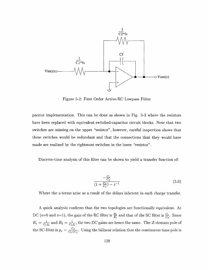
__1C2*fs
Cf
CI*fs
Vin(z) -
a a Vout(z)
Figure 5-2: First Order Active-RC Lowpass Filter
pacitor implementation. This can be done as shown in Fig. 5-3 where the resistors
have been replaced with equivalent switched-capacitor circuit blocks. Note that two
switches are missing on the upper "resistor", however, careful inspection shows that
these switches would be redundant and that the connections that they would have
made are realized by the rightmost switches in the lower "resistor".
Discrete-time analysis of this filter can be shown to yield a transfer function of:
c_ (5.6)(1+ ) -z-1
Where the z-terms arise as a result of the delays inherent in each charge transfer.
A quick analysis confirms that the two topologies are functionally equivalent. At
DC (s=0 and z=1), the gain of the RC filter is - and that of the SC filter is -. SinceRI C2
R, = 1 and R2 = fthe two DC gains are hence the same. The Z-domain pole of
the SC-filter isPz - C. Using the bilinear relation that the continuous time pole is
128
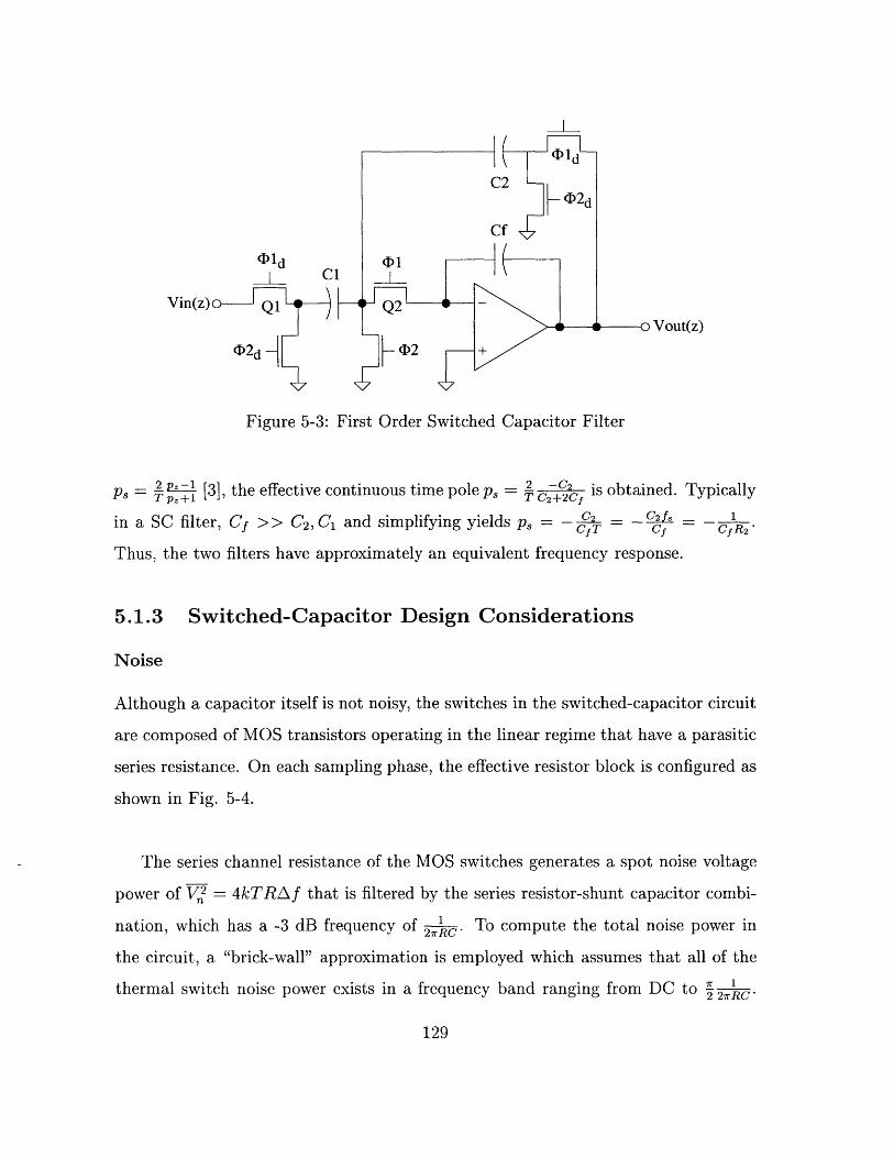
OldCQ
V in ( z ) Q i
02d
1ld
C2
Cf 0
1 Q2-
02 +
Figure 5-3: First Order Switched Capacitor Filter
Ps = i [3], the effective continuous time pole p, = 2 C2 is obtained. Typically
in a SC filter, Cf >> C2, C1 and simplifying yields p, = -g = C 2 f 1CfT Cf Cf R 2 "
Thus, the two filters have approximately an equivalent frequency response.
5.1.3 Switched- Capacitor Design Considerations
Noise
Although a capacitor itself is not noisy, the switches in the switched-capacitor circuit
are composed of MOS transistors operating in the linear regime that have a parasitic
series resistance. On each sampling phase, the effective resistor block is configured as
shown in Fig. 5-4.
The series channel resistance of the MOS switches generates a spot noise voltage
power of V,2 = 4kTRAf that is filtered by the series resistor-shunt capacitor combi-
nation, which has a -3 dB frequency of 2 1kc. To compute the total noise power in
the circuit, a "brick-wall" approximation is employed which assumes that all of the
thermal switch noise power exists in a frequency band ranging from DC to 11 12 27rRC'
129
V----o Vout(z)
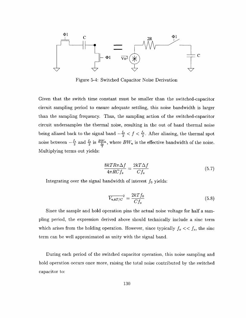
C 01C 2R
tD1 C 7
Figure 5-4: Switched Capacitor Noise Derivation
Given that the switch time constant must be smaller than the switched-capacitor
circuit sampling period to ensure adequate settling, this noise bandwidth is larger
than the sampling frequency. Thus, the sampling action of the switched-capacitor
circuit undersamples the thermal noise, resulting in the out of band thermal noise
being aliased back to the signal band -L < f < s. After aliasing, the thermal spot
noise between -E- and is , where BWn is the effective bandwidth of the noise.2
Multiplying terms out yields:
8kTRrFAf _ 2kTAf (57)47rRCf, Cfs
Integrating over the signal bandwidth of interest fo yields:
2 2kTfonk/C - Cfs (5.8)
Since the sample and hold operation pins the actual noise voltage for half a sam-
pling period, the expression derived above should technically include a sine term
which arises from the holding operation. However, since typically f << f8, the sine
term can be well approximated as unity with the signal band.
During each period of the switched capacitor operation, this noise sampling and
hold operation occurs once more, raising the total noise contributed by the switched
capacitor to:
130
Vn,kT/c 2 4kTf (5.9)
Note that this expression is again equivalent to that which would be generated by
a resistor if R = 1:Cf3
2Vn,kT/C = 4kTRfo (5.10)
Examining the expression derived above makes plain the aforementioned tradeoff
between area and noise. In order to decrease noise, the capacitances composing the
effective resistances must be large, and since it was mentioned earlier that typically
the integrating feedback capacitors are much larger than the switched capacitances,
the feedback capacitors must be very large. Interestingly, the output-referred ther-
mal noise due to a switched capacitor is approximately equal to that of its equivalent
resistor provided that the approximation R = - still holds [29].Cf3
Once the noise associated with each capacitor is computed, its contribution to the
total output-referred component noise can be calculated by multiplying the expres-
sion derived above with the effective gain seen by the capacitor to the filter output.
This effective gain can be found using an AC analysis in a tool such as SWITCAP or
SPICE.
Switch Design Tradeoffs
The MOS devices which are used to implement switches in the switched capacitor
network come with a tradeoff of their own. As implied before, when sampling onto
a capacitor through a switch, the channel resistance of the switch shunted with the
sampling capacitance results in a lowpass filter with a time constant T = RC where
R5 witch knty, ( 41)2 [32]. This time constant affects the settling ac-
131
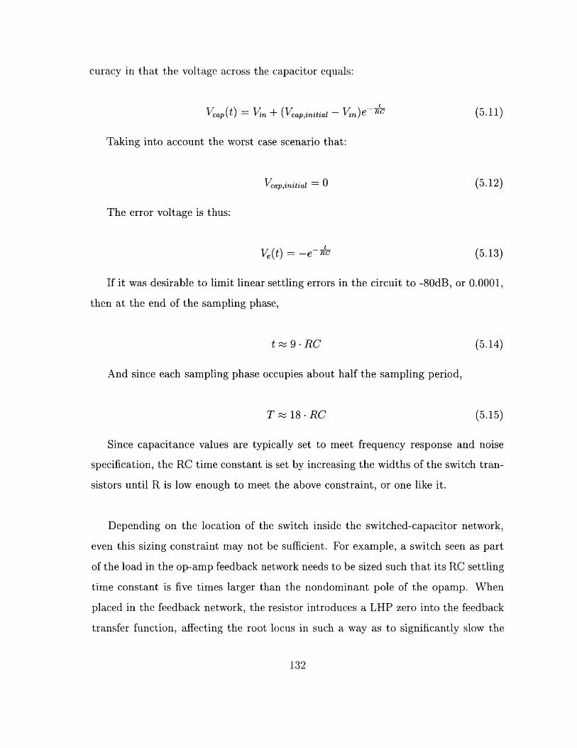
curacy in that the voltage across the capacitor equals:
Vcap(t) =Vin + (Vcap,initial - Vin)e RC (5.11)
Taking into account the worst case scenario that:
Vcap,initial = 0 (5.12)
The error voltage is thus:
Ve(t) = --- (5.13)
If it was desirable to limit linear settling errors in the circuit to -80dB, or 0.0001,
then at the end of the sampling phase,
t ~ 9 - RC (5.14)
And since each sampling phase occupies about half the sampling period,
T ~ 18 -RC (5.15)
Since capacitance values are typically set to meet frequency response and noise
specification, the RC time constant is set by increasing the widths of the switch tran-
sistors until R is low enough to meet the above constraint, or one like it.
Depending on the location of the switch inside the switched-capacitor network,
even this sizing constraint may not be sufficient. For example, a switch seen as part
of the load in the op-amp feedback network needs to be sized such that its RC settling
time constant is five times larger than the nondominant pole of the opamp. When
placed in the feedback network, the resistor introduces a LHP zero into the feedback
transfer function, affecting the root locus in such a way as to significantly slow the
132
op amp settling time [42].
Although switches with very large widths have low channel resistances, increasing
the size of the MOS devices also increases the clock feedthrough and charge injection of
the switch. Charge injection was described earlier in the context of calibrated current
sources and refers to the channel charge of the MOSFET exiting through both the
drain and the source of the transistor when it is turned off and is proportional to
WL. Clock feedthrough refers to the capacitive coupling between the gate and drain
(source) of the MOSFET through the parasitic overlap capacitances. When the clock
waveform abruptly changes the amount of charge on the overlap capacitance, some
of it appears on the load capacitance through the capacitive divider that is formed
between the overlap capacitance and the load capacitance. The voltage change on
the load capacitance can be shown to be:
AV= gCovAVate (5.16)Cload
where Cov oc W.
Although for a differential circuit, such errors are nominally common mode errors
and are canceled out by the differential nature of the circuit, it is desirable to minimize
these effects to the extent possible because of mismatch between the two differential
paths, which requires the switch sizes to be as small as possible. Of considerable
importance is the charge injected by the switch Q1 in Fig. 5-3. Since the channel
charge in this switch is signal dependent, it can introduce distortion into the signal.
On the other hand, since switch Q2 is always connected to virtual ground, its channel
charge remains roughly constant and its introduction results only in a DC offset er-
ror which is eliminated by the differential nature of the circuit or is otherwise ignored.
The channel injection from switch Q1 can be mitigated using a switching scheme
133
T/2 T/2
T/N
2T/N01
T/N~
2T/N02
Figure 5-5: Clock Switching Scheme to Reduce Distortion
such as that shown in Fig. 5-5. It is seen that by turning the switches at the opamp
virtual ground off before the switches at the input of the filter, one terminal of the
capacitor is disconnected and is floating when the switches at the input of the filter
are turned off. Since one end of the capacitor is floating, the charge on that node
cannot be changed. Hence, charge cannot be injected onto the other node and the
voltage across the capacitor remains unchanged. This technique has been shown to
reduce the total amount of distortion in switched capacitor filters [48].
It should also be noted here that, as shown in Fig. 5-5, a nonoverlapping clock
waveform is used for the two clock phases obi and 4)2 in all of the switched-capacitor
circuits described in this report. If the two phases were to overlap slightly, then direct
paths for the charge to feed forward through the circuit would arise, causing charge
134
to be lost and invalidating the intended discrete-time transfer function of the circuit.
Also, the spacing between clock phases is significantly exaggerated. Normally the
spacing is on the order of Ins whereas the on-time of each phase is on the order of
100ns for a typical oversampling switched-capacitor system.
Opamp Nonidealities
Finite Opamp Gain Although finite opamp gain nonidealities do not have the
same pernicious effects in D/A converter as they do in A/D converters, where they
cause integrator leakage and mismatch between cascaded stages, their effects must
still be taken into account in the switched-capacitor filter. In general, the finite gain
of an opamp results in a finite DC gain error in the transfer function of the opamp.
For audio filtering applications, this error causes only a slight linear gain compression
at the opamp output. A high gain is necessary, however, for the proper functionality
of the autozeroing and correlated double sampling techniques that are necessary to
reduce the effect of DC offset and 1/f noise at the input of the opamp. A typical
rule of thumb is to implement an opamp with a gain of about 80dB in order to
obtain reasonable rejection of input-referred opamp noise with the correlated double
sampling (CDS) technique. Such an opamp gain also limits linear settling errors to
0.01%.
Finite Opamp Bandwidth Finite opamp bandwidth prevents complete settling
of the voltage signal at the opamp output, even assuming that opamp slewing is
negligible or nonexistent. In order to minimize the opamp bandwidth required for a
certain degree of settling, the phase margin of the opamp must be set such that the
step response is optimally, or critically damped. Assuming that the opamp is a two-
pole system, the opamp phase margin for optimum settling for a switched-capacitor
integrator is given as: [42]
135
JMST - 900 - tan 1 [1 + (7r/0.693N) 2 (5.17)1 4
where it is assumed that switch resistance is negligible and where N is the desired
number of bits of resolution. For N=18, this results in an optimal phase margin of
about 75'.
A rough approximation to the required settling time for a settling accuracy of N
bits can be made by assuming that the opamp undergoes linear settling in response
to a step and that the time constant of the step response is given by [3}
1 1T= (5.18)
W-3dB &.9g
Where the opamp is assumed to be in a capacitive feedback configuration with
feedback factor 0. Note that in most switched-capacitor circuits, / is only slightly
less than unity, however, in topologies where correlated double sampling techniques
are employed, this may not be the case. Also note that for the remainder of this
report, further instances of # denote the feedback factor seen by the opamp and not
For a closed-loop circuit, the step response is known to be
Vot(t) = Vtep(t)(1 - e-tr ) (5.19)
And thus the settling error voltage at the end of the sampling interval, which can
be approximated as Tsett = -_, is given by:
Verror = = eTsett/
Substituting and rearranging terms yields:
136
fug 0.693Nft =..2/ (5.20)f, 0.5 - 21ro
which dictates that for N=18, the unity gain frequency in Hertz must be about 4
times greater than the switching frequency at the worst case process and temperature
corner for a 3 of unity. Since # turns out to be about 0.7, the unity gain frequency
needs to be about 5.7 times the switching frequency, where the unity gain frequency
is measured directly at the opamp output during an AC sweep measurement.
A more involved analysis by Martin, et al. [43] develops expressions and guidelines
for the design of a switched-capacitor biquad filter, and also reaches the conclusion
that to make settling error negligible, the opamp must have a unity gain frequency 5
times greater than the circuit switching frequency.
Slew Rate Since nonlinearities in the circuit are to be avoided wherever possible,
it is desirable to guarantee that the switched-capacitor opamp never enter its slewing
regime and hence contain nonlinear settling components. Note that just after a step
input to the opamp, the slope of the output will be at its maximum [3] and is given
by:
d V--VoutWt = step (5.21)
dt T
If the slew rate of the opamp is larger than this value, the opamp is guaranteed
never to slew in a switched-capacitor implementation. For a classic, Miller compen-
sated, two stage opamp, the internal slew rate is:
SRin= = Vef fWug (5.22)
where I,, is the DC bias current through each input branch of the opamp and VeffI
is the overdrive voltage of the opamp input pair transistors. As will be discussed later,
137
this voltage is typically set to be the minimum overdrive voltage that keeps the MOS
device in strong saturation. This results in the requirement that:
SRint = VefflWug > VstepWug (5.23)
For an oversampling multibit D/A converter, this requirement is typically inher-
ently met. For example, the maximum (and minimum) output step on the first opamp
in a DCT filter with a feedback to input capacitor ratio of 25 and with a 4 bit D/A
converter is Vtep = 0.005V.
5.1.4 Direct Charge Transfer
As stated in the previous chapter, the Direct Charge Transfer switched-capacitor
technique saves power by never connecting its sampling capacitor, C1 in Fig. 5-
6 below, as a load seen through the opamp feedback capacitor Cf. In addition,
for each order of postfiltering, there is only one capacitor that contributes to the
switched-capacitor noise of the filter, a slight advantage over second order biquad
filter structures, whose second-stage capacitors see a high-pass transfer function to
the filter output.
As stated before, the filter block shown above has a transfer function of:
V0st(z) z -1V jt (Z) -1 ( ±(5.24)Vi (Z) (+ Cf) - Cfz-1
which is a first-order filtering operation in discrete time.
Robust Transfer Function
One advantage of the Direct Charge Transfer technique as a filtering option is its
robust transfer function characteristics. As stated in the previous section, the 6- ab-
solute capacitor variation in the process used is approximately 1.5%. When matching
capacitor ratios as is the case in filter design, the variation in the capacitance ratio is
138
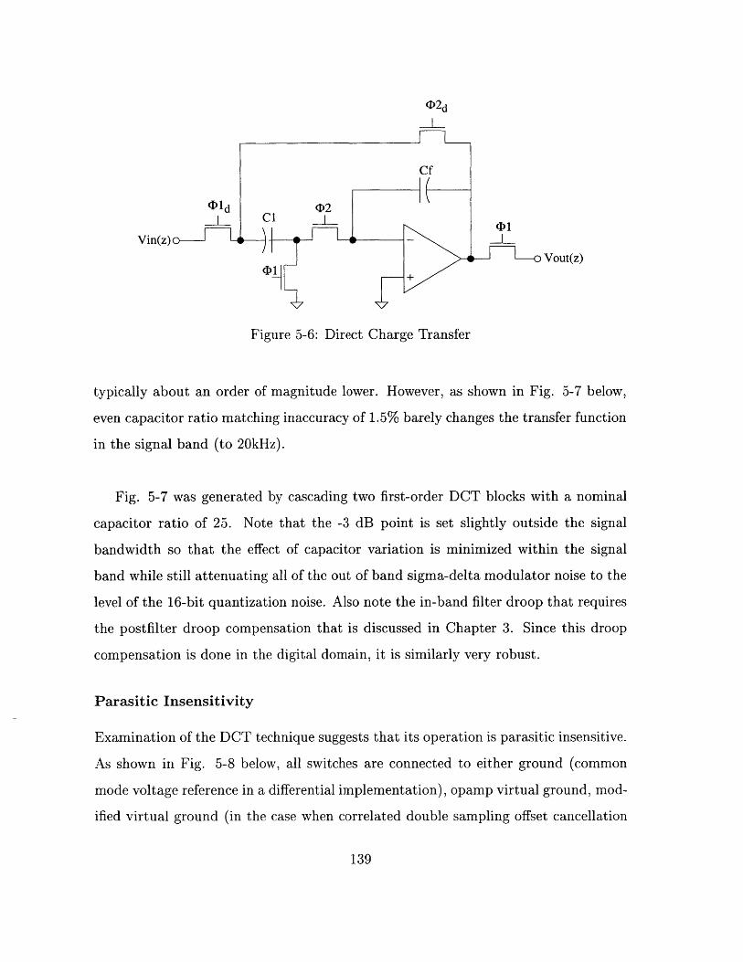
0D2d
_Cf
Ol~d 0D21S C1 D
Vin(z)c -_L-d Nvout(z)
0D1+
Figure 5-6: Direct Charge Transfer
typically about an order of magnitude lower. However, as shown in Fig. 5-7 below,
even capacitor ratio matching inaccuracy of 1.5% barely changes the transfer function
in the signal band (to 20kHz).
Fig. 5-7 was generated by cascading two first-order DCT blocks with a nominal
capacitor ratio of 25. Note that the -3 dB point is set slightly outside the signal
bandwidth so that the effect of capacitor variation is minimized within the signal
band while still attenuating all of the out of band sigma-delta modulator noise to the
level of the 16-bit quantization noise. Also note the in-band filter droop that requires
the postfilter droop compensation that is discussed in Chapter 3. Since this droop
compensation is done in the digital domain, it is similarly very robust.
Parasitic Insensitivity
Examination of the DCT technique suggests that its operation is parasitic insensitive.
As shown in Fig. 5-8 below, all switches are connected to either ground (common
mode voltage reference in a differential implementation), opamp virtual ground, mod-
ified virtual ground (in the case when correlated double sampling offset cancellation
139
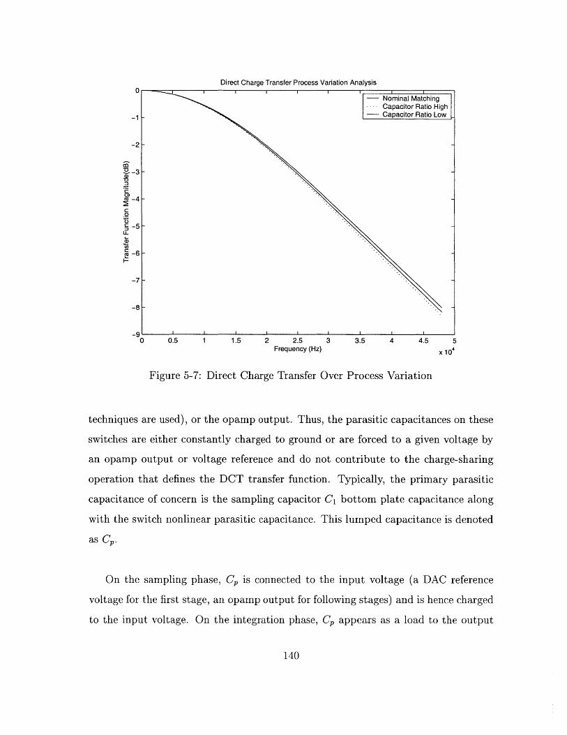
Direct Charge Transfer Process Vanation Analysis0
0 0.5 1 1.5 2 2.5Frequency (Hz)
3 3.5 4 4.5 5
x 104
Figure 5-7: Direct Charge Transfer Over Process Variation
techniques are used), or the opamp output. Thus, the parasitic capacitances on these
switches are either constantly charged to ground or are forced to a given voltage by
an opamp output or voltage reference and do not contribute to the charge-sharing
operation that defines the DCT transfer function. Typically, the primary parasitic
capacitance of concern is the sampling capacitor C1 bottom plate capacitance along
with the switch nonlinear parasitic capacitance. This lumped capacitance is denoted
as Cp.
On the sampling phase, Cp is connected to the input voltage (a DAC reference
voltage for the first stage, an opamp output for following stages) and is hence charged
to the input voltage. On the integration phase, C, appears as a load to the output
140
-1
-2
"-3-5
0)
0)
C:
-8
- Nominal Matching.... Capacitor Ratio Hig- Capacitor Ratio Lov
- -
h
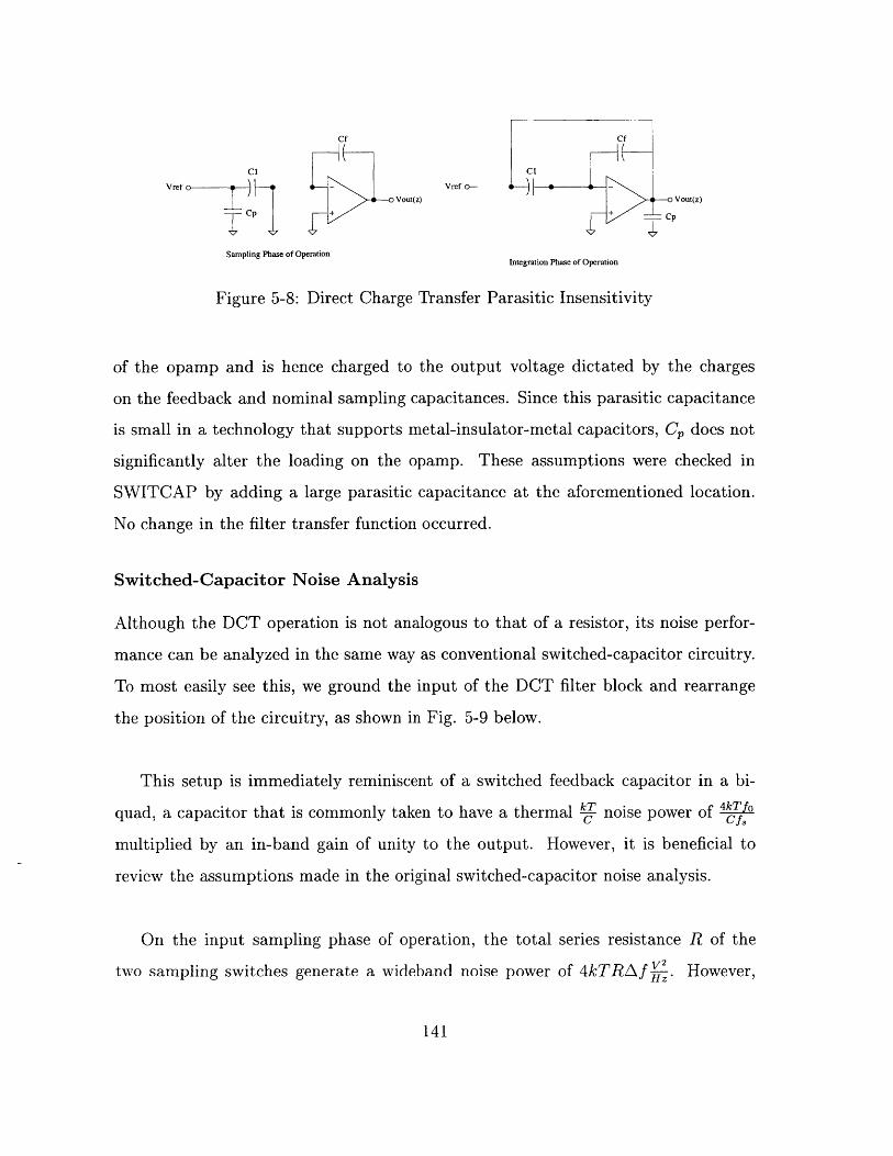
Cf Cf
CI CIVref 0 Vref o-
Vout(z) Vout(z)
Cp + + Cp
';7 TSampling Phase of Operation
Integration Phase of Operation
Figure 5-8: Direct Charge Transfer Parasitic Insensitivity
of the opamp and is hence charged to the output voltage dictated by the charges
on the feedback and nominal sampling capacitances. Since this parasitic capacitance
is small in a technology that supports metal-insulator-metal capacitors, C, does not
significantly alter the loading on the opamp. These assumptions were checked in
SWITCAP by adding a large parasitic capacitance at the aforementioned location.
No change in the filter transfer function occurred.
Switched-Capacitor Noise Analysis
Although the DCT operation is not analogous to that of a resistor, its noise perfor-
mance can be analyzed in the same way as conventional switched-capacitor circuitry.
To most easily see this, we ground the input of the DCT filter block and rearrange
the position of the circuitry, as shown in Fig. 5-9 below.
This setup is immediately reminiscent of a switched feedback capacitor in a bi-
quad, a capacitor that is commonly taken to have a thermal T noise power of 4kTfo
multiplied by an in-band gain of unity to the output. However, it is beneficial to
review the assumptions made in the original switched-capacitor noise analysis.
On the input sampling phase of operation, the total series resistance R of the
two sampling switches generate a wideband noise power of 4kTRAf v. However,
141
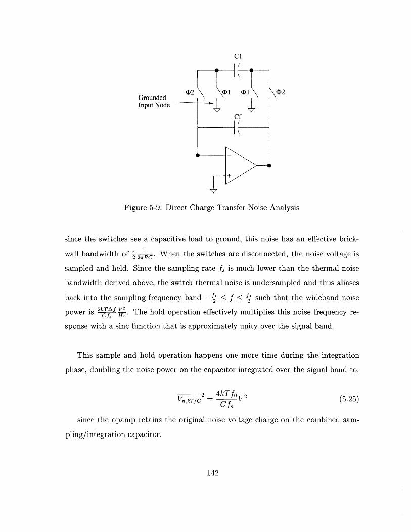
C1
Grounded 1 1 2
Input Node
Cf
Figure 5-9: Direct Charge Transfer Noise Analysis
since the switches see a capacitive load to ground, this noise has an effective brick-
wall bandwidth of !2 1C. When the switches are disconnected, the noise voltage is2 2irRC
sampled and held. Since the sampling rate f, is much lower than the thermal noise
bandwidth derived above, the switch thermal noise is undersampled and thus aliases
back into the sampling frequency band - < f Ls such that the wideband noise
power is 2kTcf 1. The hold operation effectively multiplies this noise frequency re-
sponse with a sinc function that is approximately unity over the signal band.
This sample and hold operation happens one more time during the integration
phase, doubling the noise power on the capacitor integrated over the signal band to:
2 4kTfoVnfkT/c Cfs 2 (5.25)
since the opamp retains the original noise voltage charge on the combined sam-
pling/integration capacitor.
142
Two-phase Clock Waveform Considerations
It is important to note that the delayed two-phase clock waveform shown in Fig. 5-5
also applies to Direct Charge Transfer and in fact was developed with Direct Charge
Transfer in mind [48].
RC-Equivalence
One disadvantage of DCT is that its operation does not have a clearly defined RC
analogue. For conventional switched-capacitor circuits, this equivalence provides an
advantage in some simulators such as Cadence where AC noise analyses are performed
to obtain the input-referred noise contributions of opamps. Since an AC analysis
cannot be performed on a real switched-capacitor circuit for lack of a DC path to
the output on any given clock phase, the effective resistances are set in place of the
switched capacitors to confirm the transfer functions and in-band power gain from
various points in the circuit to the filter output.
5.1.5 Correlated Double Sampling
Correlated Double Sampling with Traditional Switched-Capacitor Struc-
tures
Correlated Double Sampling is one of a larger class of autozeroing techniques that are
are used to eliminate opamp offset and finite opamp gain effects in switched-capacitor
circuits [41]. As shown in the diagram of a canonical inverting switched-capacitor inte-
grator in Fig. 5-10 below, the difference between error voltage and ground is sampled
at the negative input of the opamp on Ccd, on <b2. On the sampling/integrating phase
41 , the low frequency components of V will not have changed much, resulting in the
terminal of Ccd, opposite the opamp acting as a modified virtual ground at which the
low frequency components of V have been cancelled out.
143
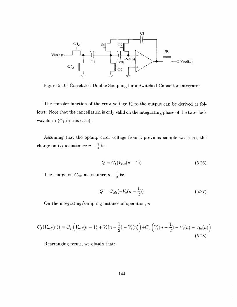
Cf
Old 011 02
Vin(n) -J
C1 Cds Vout(n)
4 2 d 2
Figure 5-10: Correlated Double Sampling for a Switched-Capacitor Integrator
The transfer function of the error voltage V to the output can be derived as fol-
lows. Note that the cancellation is only valid on the integrating phase of the two-clock
waveform (<Dl in this case).
Assuming that the opamp error voltage from a previous sample was zero, the
charge on Cf at instance n - - is:
Q = C(Vut(n - 1)) (5.26)
The charge on Ccd, at instance n - . is:
1Q = Cc,-Ve(n - -)) (5.27)
2
On the integrating/sampling instance of operation, n:
Cf (Vout(n)) = Cf (Vout(n - 1) + Ve(n ) - Ve (n))+ C (V.,,in - V) - Ve() - (n)
(5.28)
Rearranging terms, we obtain that:
144
V0st(n) - V 0,t(n - 1) = AVout = (1+ L) (Ve(n - -) - Ve(n) Vin(n) (5.29)Cf 2 Cf
Which is the result reported in Huang, et al. [44].
Taking the Z-transform yields:
- 'VVi (z) C(1+ )(Ve(1 - z1/2))V0Ut (z) = C1 (5.30)
Noting that:
Ve(n) Vos + Vnoise(n) + Vout(n) (5.31)A
where A is the low-frequency gain of the integrating opamp. Rearranging terms
can yield an expression for the total output error voltage in the operation:
1 )-Vnief 1 V0st(rn) _V 0st(n-- 1)\~
Vouterror = (+ C Vnoise() -) + A A 2 (5.32)Cf 2 A A J
Taking the Z-transform yields:
Vouterror = (1 + £L) (Vnoise(1 - z- 1/ 2 ) + (1 -- z1/2) (5.33)
Thus, a first order differentiation is performed on the input-referred opamp noise
voltage, and the finite-gain effects of the opamp also undergo a first-order differ-
entiation, increasing the effective DC gain of the integrator. Typically, the exact
magnitude of the effectiveness of this technique is determined by simulation.
One item to note is that on the integrating phase of operation, when the leftmost
terminal of the feedback capacitor (as drawn on the schematics), the primary deter-
145
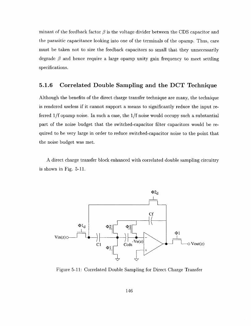
minant of the feedback factor 3 is the voltage divider between the CDS capacitor and
the parasitic capacitance looking into one of the terminals of the opamp. Thus, care
must be taken not to size the feedback capacitors so small that they unnecessarily
degrade 0 and hence require a large opamp unity gain frequency to meet settling
specifications.
5.1.6 Correlated Double Sampling and the DCT Technique
Although the benefits of the direct charge transfer technique are many, the technique
is rendered useless if it cannot support a means to significantly reduce the input re-
ferred 1/f opamp noise. In such a case, the 1/f noise would occupy such a substantial
part of the noise budget that the switched-capacitor filter capacitors would be re-
quired to be very large in order to reduce switched-capacitor noise to the point that
the noise budget was met.
A direct charge transfer block enhanced with correlated double sampling circuitry
is shown in Fig. 5-11.
Vid
Vin(z)O -j -
02d
021 Dj ICf
1 +
t1)
Vout(z)
Figure 5-11: Correlated Double Sampling for Direct Charge Transfer
146
Assuming that at the beginning of the filter's operation, the input-referred opamp
error voltage is zero, the charge on Cf at instance n - 1 is:
Q = C(Vt(n - 1)) (5.34)
The charge on Ced, at instance n is:
Q = Ccds(Ve(n) - Ve(n - (5.35)
The charge on C1 at instance n - 1 is:
1C1 (Vin(n - )) (5.36)
2
On the integrating phase of operation,
(Cf+C1) (Vot(n) - Ve(n) + Ve(n - 1) + Ve(n)) Cf (Vout(n - 1))+C 1 (Vi.(n - )
(5.37)
Rearranging and taking the Z-transform, we obtain:
-1/2 (1 + c-L)(V(1 - z 1 / 2 ))Vot in _+ C1 e(5-38)
(+ Cf) - Cfz-1 (1+ f) -- gz-1
Note that although the discrete-time differentiated error term is multiplied by
(1 + e), it has the same relative magnitude to Vin as in the case of the switched-
capacitor integrator.
Another way to look at the problem is to note that the core charge sharing oper-
ation of DCT occurs independently of the input-referred error voltage of the opamp.
Thus, on the integrating phase of operation, the output has the correct output voltage
plus
147
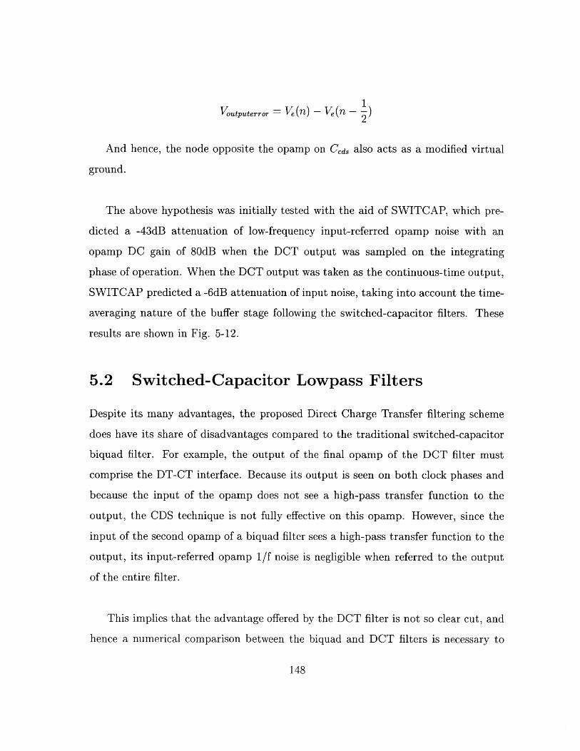
Voutputerror = Ve(n) - Ve(n - 1)2
And hence, the node opposite the opamp on cds also acts as a modified virtual
ground.
The above hypothesis was initially tested with the aid of SWITCAP, which pre-
dicted a -43dB attenuation of low-frequency input-referred opamp noise with an
opamp DC gain of 80dB when the DCT output was sampled on the integrating
phase of operation. When the DCT output was taken as the continuous-time output,
SWITCAP predicted a -6dB attenuation of input noise, taking into account the time-
averaging nature of the buffer stage following the switched-capacitor filters. These
results are shown in Fig. 5-12.
5.2 Switched-Capacitor Lowpass Filters
Despite its many advantages, the proposed Direct Charge Transfer filtering scheme
does have its share of disadvantages compared to the traditional switched-capacitor
biquad filter. For example, the output of the final opamp of the DCT filter must
comprise the DT-CT interface. Because its output is seen on both clock phases and
because the input of the opamp does not see a high-pass transfer function to the
output, the CDS technique is not fully effective on this opamp. However, since the
input of the second opamp of a biquad filter sees a high-pass transfer function to the
output, its input-referred opamp 1/f noise is negligible when referred to the output
of the entire filter.
This implies that the advantage offered by the DCT filter is not so clear cut, and
hence a numerical comparison between the biquad and DCT filters is necessary to
148
Switcap AC Response of CDS Effectiveness
0
-5
-10
-15
2 -20
-25
-30-
-35-
-40-
-45E101 10 2 10 4
Frequency(Hz)
Figure 5-12: Correlated Double Sampling SWITCAP Simulation for DCT
determine which is superior from a low-power, low-area perspective.
5.2.1 Switched-Capacitor Biquad Filter Analysis
Biquad filters are a common choice for switched-capacitor implementation because
they draw upon the vast body of work that has been performed on their continuous-
time implementations. Perhaps more practically, biquad filters permit the use of
complex poles in the filter transfer function, allowing the system designer to design
a maximally flat frequency response over the signal band and hence do not require
droop compensation.
149
- - Continuous CDS.No CDS
- Sampled CDS
10 3 10 5 10 6 107
Biquad filters are typically designed for either low or high filter Q such as to
minimize the effect of component mismatch [3]. Lowpass biquad filters used in D/A
applications are often designed with a Q slightly greater than that required to pro-
duce an optimally flat response (0.7) in order to steepen the rolloff immediately after
the pole frequency. This section will, as an exercise, go through the design of a low
Q filter with a Q of 0.8.
Derivation of Capacitor Ratios
It is known that for a stable biquad filter with the Q mentioned above, the two
continuous time poles required to generate a "-3dB" point at 24kHz are, in units of
rad/sec:
= -90368 + j113046, s 2 = -90368 - j113046
A convenient approximation to the DT-CT bilinear transform that is valid for a
reasonably large OSR is given by the relation [4]:
zi = e = ef (5.39)
For an oversampling ratio of 128 and hence fs=#=6144000Hz,
zi = 0.98523 + jO.01813, z2 = 0.98523 - jA.01813
We know that for a switched-capacitor biquad, we have a transfer function that
can be used to determine the capacitor ratios. This transfer function is expressed as:
-AzHq = z 2 BzC (5.40)
Since the poles have been determined, the coefficients A, B, and C are likewise
150
determined:
B = -(zi + z2 ) = eT9 + efs
Since s, and s2 form a conjugate pair with the same real part:
Re } coB = -2e fs (COS ( ImS i))
(5.42)
(5.43)
Since si and s2 form a conjugate pair with the same real part:
(5.44)
Because a DC gain of unity is desired,
(5.45)
From these variables and from discrete-time flowchart analysis of the biquad, a set
of constants can be derived that relate directly to the capacitor ratios in the biquad,
shown in Fig. 5-13. Treating the capacitors C and Ca as design parameters, the
following relations hold:
Ce = -Cak51
Cd = -C
1Cb = -Ca
k5
(5.46)
(5.47)
(5.48)
(5.49)
Note that Cd and Cb are the dominant area consumers of this design. The con-
151
(5.41)
C1 += 2C = Z1 Z2 =e fs
2Re{s 1 }C = e fT
A = 1+ B +C
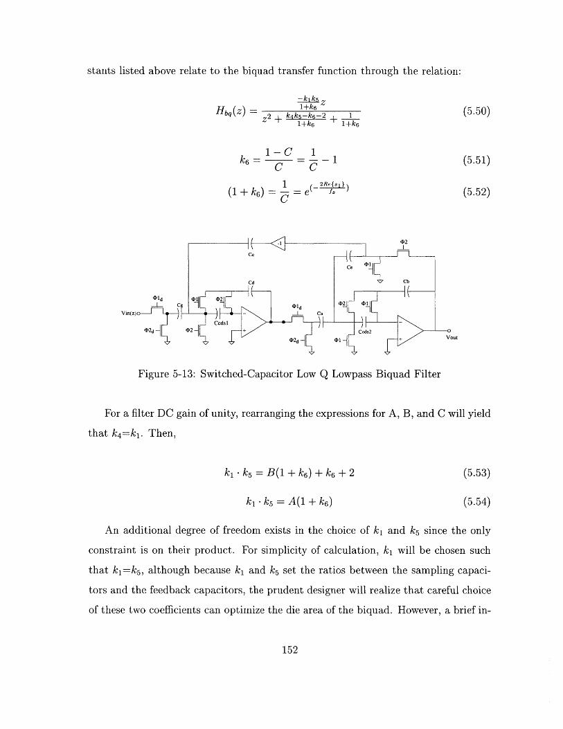
stants listed above relate to the biquad transfer function through the relation:
-kjk5 Z
-b (Z1+k 6 (-0Hbq~j - z2 + k 4k 5 -kr6 -2 + 1 (5.50)
1+k 6 1+k 6
1-C 1k6 -- 1 (5.51)
C C
1 2Refsj}(1+k )- 1 - (A (5.52)
Cc
Ce
Cd Cb
C <Dd
Vin(z) Ca
02d 02 CCdss
> L 2d Zd (P Vout
Figure 5-13: Switched-Capacitor Low Q Lowpass Biquad Filter
For a filter DC gain of unity, rearranging the expressions for A, B, and C will yield
that k4=ki. Then,
ki - k5= B(1 + k6) + k6+2 (5.53)
ki - k5= A(1 + k6 ) (5.54)
An additional degree of freedom exists in the choice of k, and k5 since the only
constraint is on their product. For simplicity of calculation, k, will be chosen such
that kirk 5 , although because k, and k5 set the ratios between the sampling capaci-
tors and the feedback capacitors, the prudent designer will realize that careful choice
of these two coefficients can optimize the die area of the biquad. However, a brief in-
152
spection for the implementation described herein reveals that such optimization only
results in an area savings of 20% over the choice of k, = k5 .
Proceeding, we have:
k4 = k5 = k1 = A(1 + k6 )
For an oversampling ratio of 128, this yields:
k6= 0.02985
kI = k4= k5= 0.02373
For analysis purposes, we can rewrite Equation 5.55 as:
1+B+C 1 Bki - +-+1
2Re{sj}
=e~ f-Re{s 1 } sim {
- 2e h (cos-1( ) +
(5.55)
(5.56)
To illustrate the tradeoff between OSR and area here, we will approximate:
(cos-1Im{s1 }
fs(5.57)
thus yielding:
Re{sj}
ki =e s -1 (5.58)
From the formulae given above, these coefficients are related to the key capacitor
ratios by the relations:
153
Cd~ C9 (5-59)C e fs -1
Ca (5.60)b Rels 1
e- fa - 1
These relations reveal a key tradeoff in the design of low-area D/A converters, thatRe{s
1 }is, as the OSR, and hence f, increase, the term e fT becomes closer to unity and
hence the denominators of the above two relations becomes closer to zero, increasing
exponentially the ratios of the sampling to feedback capacitors. Thus, it is vital to
minimize the oversampling ratio of the D/A converter in order to save die area in the
analog postfilter.
Transfer Function to Output and Switched-Capacitor Noise
Using SWITCAP, the transfer functions from various points in the circuit to the filter
output were determined, allowing the calculation of the total output-referred noise of
the filter.
Opamp Inputs From the input of the first opamp, a DC power gain of 4=6dB was
seen to the output.
From the input of the second opamp, a high pass transfer function approximately
of the form: 20.3935 -logo(f) - 81.0644dB was seen to the output. Integrating over
the signal band,
20000Hz 20.3935.log10(f)-81.0644 2Noise Power Gain =0Hz (10 20 )2f df (5.61)
20000HzNoise Power Gain = /2Hz 3-0395 . 10-8.10644 (5.62)
154
10--8.10644 1 20000Noise Power Gain = -0f2 .0395 = 1.53022 (5.63)
3.0395 .120
Capacitors Both C. and C, see a unity gain transfer function to the output.
Capacitor Ca sees a high pass transfer function approximately of the form: 20.252.
loglo(f) - 87.968dB to the output. Integrating over the signal band, this represents
a total power gain of:
10-8.7968 20000Noise Power Gain = - f2.0252 = 0.27 (5.64)
3.0252 20
Capacitor Ce sees a high pass transfer function approximately of the form: 19.594.
loglo(f) - 83.13dB to the output. Integrating over the signal band, this represents a
total power gain of:
108.313 120000Noise Power Gain = 2.594 f 1.9594 = 0.44 (5.65)
2.9594 20
5.2.2 Direct Charge Transfer Filter Analysis
The direct charge transfer filter consists of two identically ratioed filter blocks, al-
though like the biquad capacitor the two sampling capacitors C1 and C2 can be
independently set. Using a similar analysis as for the biquad filter, it is possible to
set the capacitor ratio.
Derivation of Capacitor Ratios
From the transfer function of a first-order DCT filter, it can be seen that a discrete
time pole exists at:
z Cf (5.66)C + C1
And that the ratio between the sampling and feedback capacitors is given by:
155
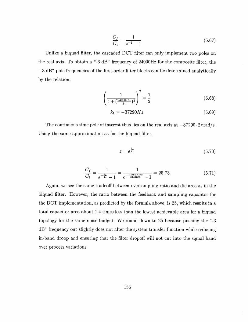
Cf _ 1 (5.67)C1 z-1
Unlike a biquad filter, the cascaded DCT filter can only implement two poles on
the real axis. To obtain a "-3 dB" frequency of 24000Hz for the composite filter, the
"-3 dB" pole frequencies of the first-order filter blocks can be determined analytically
by the relation:
1 + (24000Hz2 (5.68)
k, = -37290Hz (5.69)
The continuous time pole of interest thus lies on the real axis at -37290- 27rrad/s.
Using the same approximation as for the biquad filter,
z = e7 (5.70)
Cf r 1 1- 27- -2.37290 25.37 (5.71)C1 efs I e- 6144000- 1
Again, we see the same tradeoff between oversampling ratio and die area as in the
biquad filter. However, the ratio between the feedback and sampling capacitor for
the DCT implementation, as predicted by the formula above, is 25, which results in a
total capacitor area about 1.4 times less than the lowest achievable area for a biquad
topology for the same noise budget. We round down to 25 because pushing the "-3
dB" frequency out slightly does not alter the system transfer function while reducing
in-band droop and ensuring that the filter dropoff will not cut into the signal band
over process variations.
156
Transfer Function to Output and Switched-Capacitor Noise
Intuition and SWITCAP analysis show that the power gain from each node in the
DCT structure to the filter output is unity.
5.3 Opamp Design for Switched-Capacitor Filters
Knowing the capacitor ratios along with the network structure of both topologies
permits the calculation of output-referred kT/C noise, the dominant consumers of die
area of the circuit, and a set of effective output loads for the two opamps. However,
in order to design the filter holistically, it is important to first lay down the principles
by which the opamps will be designed.
5.3.1 Topology Choice
Before designing the opamp itself, the opamp topology must be chosen. As stated
earlier, the requirements of the two opamps are:
1. High Linearity
2. DC Gain > 80dB
3. Unity Gain Frequency > 4f, on slow process corner
4. Optimal settling on slow process corner (when f-3dB is the lowest)
5. Low Noise
Class A opamps were chosen over class AB opamps for this project because of their
superior linearity performance and because their power dissipation can be predicted
and optimized in a straightforward manner [45]. Since each output of the opamp
must swing 1.625V through a 2.5V supply voltage, the swing has only about 400mV
headroom on either end. This headroom is insufficient to keep the resistance of a
wide-swing cascode relatively constant over the maximum voltage swing and thus
157
we require that the output stage of the opamp consist of only one NMOS and one
PMOS transistor. Of course, with such an output stage, a separate input stage is
also required in order to achieve 80+ dB of DC gain. Since the bandwidth specifica-
tion should be easy to meet, the opamp topology that comes to mind is the classic
Miller-compensated two-stage opamp.
The schematic of such an opamp is shown in Fig. 5-14
5.3.2 Assigning Overdrive Voltages to Key Transistors
The first task to be performed while designing an opamp is to design the transistors of
the input stage (M1-M4) to minimize voltage offset as a result of sizing and threshold
voltage mismatches.
For the input pair of transistors (M1-M2), the gate offset voltage must be minimized.
Given that the MOSFET saturation current relation is given by:
1 WID - VT) 2 (5.72)
The gate voltage mismatch can be approximated by [25]
6V,-= 6VT + ( VGS-VT)( 6W+ 6L (5.73)2 W L
Thus, the gate overdrive voltage Veff = VGS - VT must be kept as low as possi-
ble while maintaining the device in strong inversion. This limit is typically around
Veff = 0.18V for a 0.25pm process. Note that this arrangement for Veff maximizes
transconductance per current, which is important for transistors M1, M2, M7, and
M9. Also note that Veff=VDS,sat and thus this voltage needs to be minimized for M7
and M9 to maximize voltage swing and thus to reduce distortion at the output node.
158
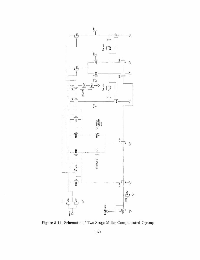
Figure 5-14: Schematic of Two-Stage Miller Compensated Opamp
159
00
<02
F
nD
.T-
For the current source active load in the input stage (M3-M4), current mismatch
results in a gate voltage offset when referred back to the input pair (M1-M2). The
objective here is thus to minimize current mismatch. If channel length and threshold
voltage are independent, the drain current mismatch is [25]:
ID _ 6W 6L 2 6 VTID W L (VGS - T7)
Thus, Veff on M3 and M4 must be kept large. In practice, channel length and
threshold voltage are not independent [49} and voltage swing requirements dictate
that Vff not be too large. Typical design values for Veff on these transistors range
from 0.3V to O.4V.
5.3.3 Gain
The gain of a two-stage opamp is typically large, with the only parameter under the
control of the designer being the lengths of the transistors. However, it is undesirable
to increase the lengths of transistors MI and M2 because they form a considerable
portion of the load seen by the opamp and decrease 3 when increased. It is also unde-
sirable to increase the lengths of M7 and M9 because their gate capacitances decrease
the frequency of the non-dominant pole, reducing the opamp's phase margin.
As following analysis will show, however, it is desirable to increase the lengths
of transistors M3 and M4 in order to reduce opamp input-referred thermal and 1/f
noise. Gain is usually sufficient at this point to necessitate increasing the lengths of
M6 and M8. Assuming that LI- 2 ,5 -8 = 1pm and that L 3- 4 = 8pam, the total gain of
the opamp is:
A = g.1 (roi//To2 )gm7(ro6//ro7 ) (5.75)
A 2I 217 (5.76)Vef f1A', Vef f7 (An + Ap)I 7
160
2 2A ~, 2 (5.77)Vef fijA Veff 7 (An + Ap)
For approximation purposes, we take Veffl = Veff7 = 0.18V, An = 0.1V 1 , and
AP = 0.05V- 1 to find that A = 16500, or 84dB.
5.3.4 Bandwidth
The bandwidth of the opamp is defined by its unity gain frequency Wug. For a two-
stage opamp,
Wug = mi (5.78)Cc (Veff1)Cc(
As stated earlier, wug must be greater than 4*OSR*48000Hz for the slow process
corner. This occurs for a slow process and low temperature, when the PTAT current
source supply current is at its minimum. Designing for the nominal case, a correction
factor of 1.3 guarantees that the bandwidth specification is met over all corners.
Thus, the input branch current of the opamp is set by treating the compensation
capacitance as a design variable and is hence constrained to be:
1 5.2 -OSR -48000Hz -C (579)
2#
5.3.5 Phase Margin
A typical rule of thumb to designing optimally compensated opamps is to place the
nondominant pole approximately three times away from the closed-loop crossover
frequency W-3dB. This sets the phase margin Om to be:
Om = 900 - tan-1 (w-3dB/wnd) = 900 - tan-(1/3) = 71.60 (5.80)
We note that is slightly cumbersome to relate the opamp parameters to W-3dB if
3 < 1. However, if / < 1 and the frequency of the nondominant pole is set to 3 wug,
161
the actual phase margin will be slightly higher than 71.60 and will thus be closer to
750. Thus, the hand design will be carried out assuming that Wnd ~ 3w,,. In addition,
the lead compensation of the two-stage opamp is the final determinant of the phase
margin, and hence this relation is merely useful in setting the nondominant pole to a
frequency at which such compensation is easily achieved.
In a two-stage opamp, the nondominant pole
frequency:
_gm7/3
Wnd - CLoad,OL
1 + Cs7c
Where CLOad,OL is the load capacitance seen at
calculation is often performed by calculating an
CLoad,CL - CLoadOL and writing:
is approximately located at the
(5.81)
the output of the amplifier. This
effective closed loop capacitance
(5.82)_9m7
Wnd = CLoadCL
1 Cgs 7
For design purposes, it is desirable to solve for gm7 as a function of Cload and Cc,
as these two parameters will set the power through the output stage of the device.
Solving for 9m7
Realizing that:
9m7= Lt nCoxVeff7
Cs7 W2W3 L
(5.83)
(5.84)
Rearranging terms yields:
C 2s7 = Y COXPnCoxVeff7
(5.85)
162
9m7
Wnd = fo"d (5.86)Wnd L 2 Cox
+InCoxVeff7 Cc
Noting that Wnd = 3 wg and solving for 9m7 yields:
3 wugCLoad9m7 1 _ sosCLoad fLCox (5.87)
Also noting that the static current required to flow through the output stage is:
117 = gm7Veff 7 (5.88)
1 3WgCLoadVeff7I7 = - (5.89)
2 1 _3wu9CLoad-dL2C..Ccyn Cox Vef f7
Calculating Load Capacitance
The effective closed loop load capacitance seen by the opamp is equal to:
CLoad,CL = Ci + Op + (5.90)
where C1 is the sampling capacitance seen through the feedback network, C is the
effective opamp parasitic input capacitance seen through the feedback networks, and
C2 is the effective capacitance seen at the output of the opamp. These capacitances
C1 and C2 vary with the phase of operation, however, the worst-case scenario is not
difficult to predict.
The worst-case loading scenario for the biquad filter opamp exists on the integrating
phase of operation, when the opamp sees the sampling capacitance and when # is at
its smallest due to the CDS capacitor. In this phase of operation, the CDS capacitor
appears in series with the parasitic capacitance of the opamp, resulting in a capaci-
tance smaller than the parasitic capacitance appearing in parallel with the sampling
capacitance. Typically the CDS capacitor is sized to be the same as the dominant
163
load capacitance driven on this phase of operation, because the CDS capacitor forms
the dominant load on the second phase of operation.
C2CLoad,BQ - C 1 + Cp + -- (5.91)
where C, is the opamp input parasitic capacitance plus the CDS capacitor in series.
The worst case loading scenario for the DCT filter opamp also occurs on the in-
tegrating phase of operation when # is degraded through the CDS operation. Note
that if the CDS capacitor equals the output capacitance driven by the opamp, the
loading on the opamp is approximately equal to the value of the output capacitance
C2 over both phases of operation.
CLoad,DCT ± C Cp (5.92)
5.3.6 Input-Referred Noise
An operational amplifier is an inherently noisy device, with most of its input-referred
noise being generated by the transistors in its input stage. The channel resistance
in the transistors generates a thermal noise current which can be referred back to
the input voltage of the opamp. In addition, imperfections in the gate oxide of the
transistors generates a low frequency 1/f noise voltage that can also be referred back
to the opamp input.
Thermal Noise
The gate-referred thermal noise voltage of a MOS transistor is given by:
n--2 8 kTAf2T =k- f(5.93)
3 gm
164
Often, a more conservative estimate is used where:
2 4kTAfV,T = (5.94)
We are concerned about the noise contributions from both the input pair transis-
tors (M1-M2) and from the input stage current source transistors (M3-M4). To obtain
the contributions of the latter two transistors, the noise current is first obtained:
7_2In3,T = 4kTgm3 /\Af (5.95)
Since this noise current appears in the input pair (M1-M2), it can be referred to
the input terminals through multiplication by: ( 1)2.
Thus, after appropriate substitution, term cancellation, and integration of the
white noise over the signal band of 20kHz, the total input-referred thermal noise can
be given by:
2 4kT - (20000Hz) An L(V,T = 1 + W, (5.96)
' imp Cox 1 L PLi
This thermal noise power has a bandwidth equal to the effective "brick-wall"
bandwidth of the opamp, which is constrained by opamp settling requirements to
be greater than the sampling frequency. If the signal from the input of the opamp
is sampled before reaching the output of the filter, the noise is undersampled and
aliases back into the baseband. Although this is the case for both topologies as
implemented in this report, this would not be the case for a DCT filter that has not
been enhanced with correlated double sampling, as the thermal noise at the input of
the opamp will not fold due to undersampling [33]. We note that the second DCT
filter has been enhanced with CDS because the reduction in 1/f noise is greater than
the aliasing increase in thermal noise. Finally, the aliased thermal noise power must
be multiplied by a factor of 2 to account for the differential nature of the circuit and
165
must be multiplied by the power gain from the opamp inputs to the output. Thus,
for the biquad filter,
2 =2(wugE) 4kT - (20000Hz)Vn T 2wf K 4 C- 1 +
2i L,Co 1 '
4kT - (20000Hz).L5, - 2 1,2!LLo 1,2
131PnL 3 ,11 P1
...PPL ,
W3,2AnL 3 ,2
W1,2AtP L 1 , 2 )
(5.97)
For the DCT filter,
2(wug 11) 4kT - (20000Hz)V7- =o2x- 1 +
2,r 2MCo I1,1'4
W3,4kT - (20000Hz) + 11nL3,
11+ Wi,2
29CL 1,2
W3 ,An L
'W+il.l
) (5.98)
1/f Noise
For the biquad filter, we assume that the 1/f noise is sufficiently attenuated by the
high-pass transfer function of the CDS circuitry for the first opamp. Although the
second opamp only achieves a benefit of 6dB attenuation of 1/f noise due to its CDS
circuitry, the fact that its inputs see a high-pass transfer function to the output jus-
tifies the neglect of the 1/f noise component of this opamp as well.
For the DCT filter, we also assume that the 1/f noise is sufficiently attenuated by
the high-pass transfer function of the CDS circuitry for the first opamp. The second
opamp, however, achieves only a 6dB attenuation of 1/f noise across the signal band,
as shown in Fig. 5-12. Its contribution to the total output-referred filter noise, ac-
counting for the differential nature of the circuit and the CDS attenuation, is given by:
166
2 f2k f 00 p.2828 f 2k-2 f2OOO f0.8824 m3Vnf 4 4.+(5.99)4 - W L1Cox 4 -W 3 L 3 Cox ,2
5.4 Hand Design for Noise Budget
In order to compare the biquad and DCT filter topologies, the equations derived
above will be utilized to construct a preliminary hand design of the two filters for the
same noise budget. This noise budget can be constructed using the sigma-delta SNR
for an oversampling ratio of 128 found in Chapter 4 along with the output-referred
swing and noise requirements.
At the output of this filter, the maximum output voltage swing must be 3.25Vpp
and the total rms noise voltage power must be no greater than:
F 3.25 - 2
Total Noise Power Budget = __ = 13.2 - 10- 10V2 (5.100)10 20
From Table 3.2, the simulated SNR of the digital portion of the D/A converter
is 98.36dB. Thus, the output-referred voltage noise power from the digital portion of
the D/A converter is given by:
3.25 12
Vns2 = 2 v2 = 1.93. 10- 10 V 2 (5.101)10 20
Finally, the average reference noise voltage power is given by:
Vn,,ef = 0.73 -10 0 V 2 (5.102)
167
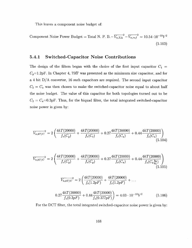
This leaves a component noise budget of:
Component Noise Power Budget = Total N. P. B.-Vn,2 Vnr 2 10.54 10 0V2
(5.103)
5.4.1 Switched-Capacitor Noise Contributions
The design of the filters began with the choice of the first input capacitor C1 =
Cg=1.2pF. In Chapter 4, 75fF was presented as the minimum size capacitor, and for
a 4 bit D/A converter, 16 such capacitors are required. The second input capacitor
C2 Ca was then chosen to make the switched-capacitor noise equal to about half
the noise budget. The value of this capacitor for both topologies turned out to be
C2 = Ca=0.3pF. Thus, for the biquad filter, the total integrated switched-capacitor
noise power is given by:
2 _ kT(20000) 4kT(20000) 4kT(20000) 4kT(20000)VnkT/c 2 (4k+ 0.2 + 0 .4 44T20)
- fs(C) + fS(CC) fs(Ca) fs(Ce)(5.104)
2 4kT(20000) 4kT(20000) 4kT(20000) 4kT(20000)Vn,kT/c = 2 f f(Cg + +0.27 +0.44 /
fs(Cg) fs(Ca) fs(Ca ) )(5.105)
2 4kT(20000) 4kT(20000)Vn,kT/c = 2 fS( 1.2pF) fs(1.2pF)
4kT(20000) 4kT(20000) N _0.27 +±0.44 =40 01V 516fs(0.3pF) fs(0.377pF)) -
For the DCT filter, the total integrated switched-capacitor noise power is given by:
168
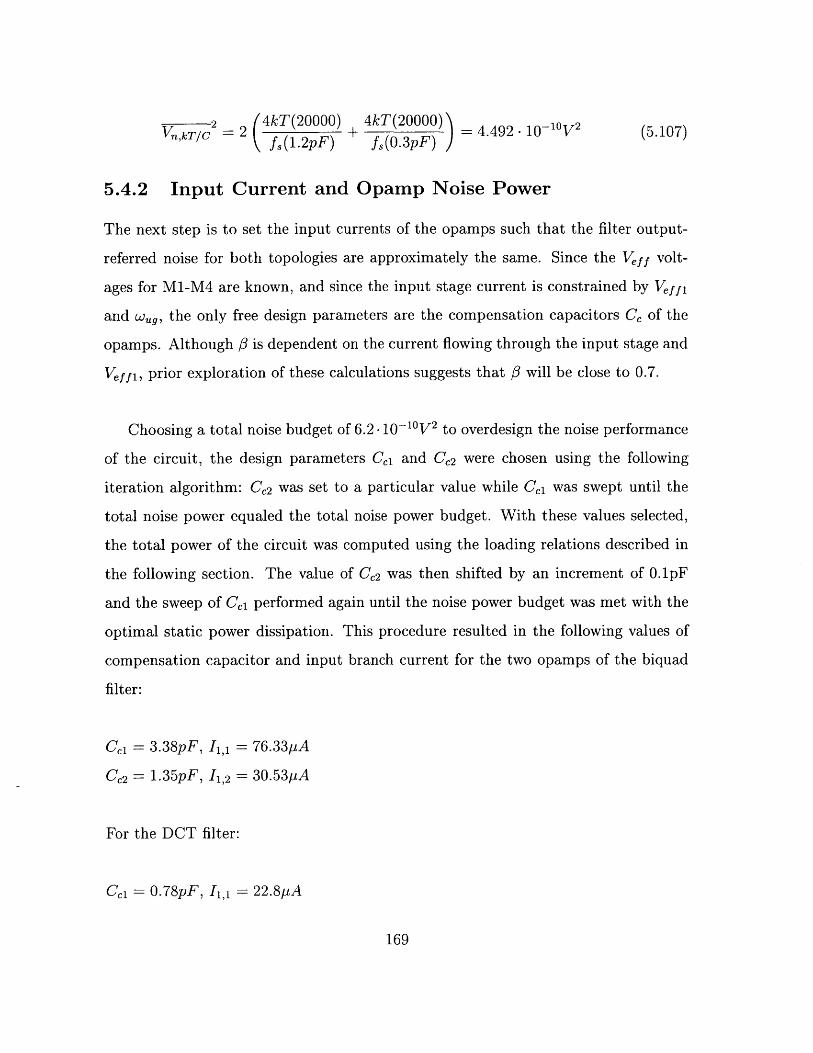
2 /AkT (20000 ) 4kT (20000)\Vn kT/c = 2 I + = 4.492 - 10- 10 V2 (5.107)
fs(1.2pF) fs(0.3pF)
5.4.2 Input Current and Opamp Noise Power
The next step is to set the input currents of the opamps such that the filter output-
referred noise for both topologies are approximately the same. Since the Veff volt-
ages for M1-M4 are known, and since the input stage current is constrained by Veff1
and w 9 , the only free design parameters are the compensation capacitors C, of the
opamps. Although # is dependent on the current flowing through the input stage and
Veffl, prior exploration of these calculations suggests that 3 will be close to 0.7.
Choosing a total noise budget of 6.2- 10- 10V2 to overdesign the noise performance
of the circuit, the design parameters Cci and Cc2 were chosen using the following
iteration algorithm: Cc2 was set to a particular value while Cc1 was swept until the
total noise power equaled the total noise power budget. With these values selected,
the total power of the circuit was computed using the loading relations described in
the following section. The value of Cc2 was then shifted by an increment of 0.1pF
and the sweep of Cc performed again until the noise power budget was met with the
optimal static power dissipation. This procedure resulted in the following values of
compensation capacitor and input branch current for the two opamps of the biquad
filter:
Cci = 3.38pF, 11,1 = 76.33puA
C,2= 1.35pF, 11,2 = 30.53pA
For the DCT filter:
Cci = 0.78pF, I1,1 = 22.8pA
169
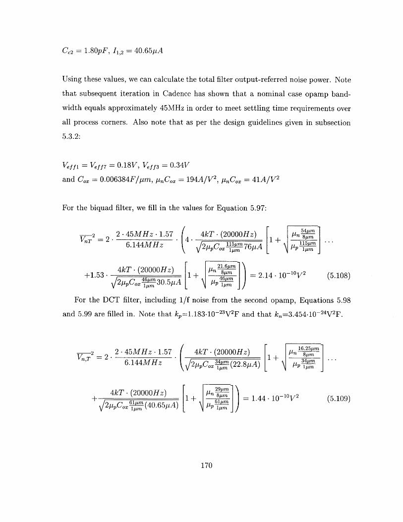
Cc2 = 1.80pF, I1,2 = 40.65puA
Using these values, we can calculate the total filter output-referred noise power. Note
that subsequent iteration in Cadence has shown that a nominal case opamp band-
width equals approximately 45MHz in order to meet settling time requirements over
all process corners. Also note that as per the design guidelines given in subsection
5.3.2:
Veffl = Vef 7= 0.18V, Veff 3 = 0.34V
and C,, = 0.006384F/pm, pjiCx = 194A/V 2, putC,, = 41A/V 2
For the biquad filter, we fill in the values for Equation 5.97:
. (4-
4kT - (20000Hz)
2 pQCx 46' 30.5/pA
4kT - (20000Hz)
2tpCox 1m"76pA
For the DCT filter, including 1/f noise from the second opamp, Equations 5.98
and 5.99 are filled in. Note that kp=1.183-10- 2 3V2 F and that k,=3.454.10- 2 4 V2 F.
2VTr =2.-
2 - 45MHz - 1.57
6.144MHz
4kT - (20000Hz)
/2ppCox 6 (40.65/p A)
4kT - (20000Hz)
2ppCox (22.8pA )S1+
8gm -1.44- 10-1 0 V2
\P 1gm
170
2 2 .45MHz -1.57VT = 2 -
6.144MHz
+1.53-
1+
54gm]
,115gm1gm
21.6gpm
+ 8m = 2.14-\ 46m1glm )J
10-100V2 (5.108)
+
16.25gm\n 8.m
34pm-t P 1gimj
(5.109)
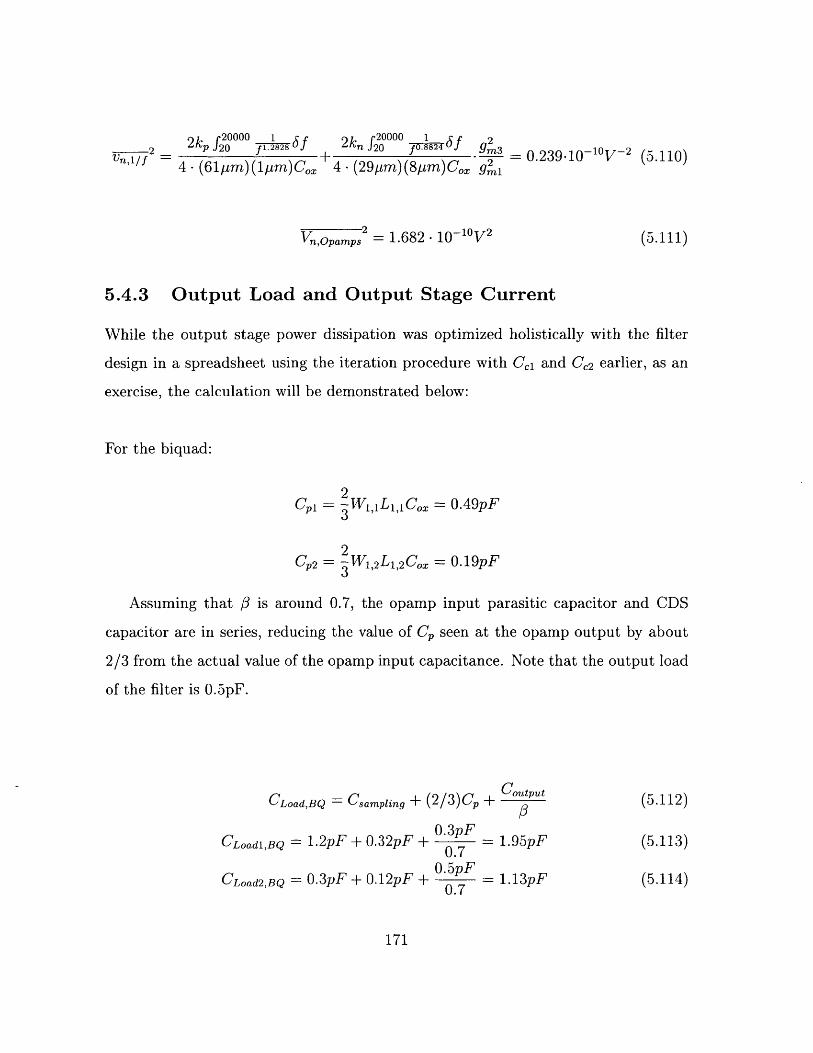
2kp f220000 1.2828 6f 2kn f O 0.08824 6f g2±2 f 1 + m3 = 0.239-10- 10V- 2 (5.110)
Vnl/f 4 - (61pm)(lIIm)C 4 - (29pim)(8pTm)C. g2
Vn,Opamps2= 1.682 - 10- 10 V2 (5.111)
5.4.3 Output Load and Output Stage Current
While the output stage power dissipation was optimized holistically with the filter
design in a spreadsheet using the iteration procedure with Cc1 and c2 earlier, as an
exercise, the calculation will be demonstrated below:
For the biquad:
2Cp1 = --W1,1L1,1C0x = 0.49pF3
2Cp2 = --W1,2L1,2Cox= 0.19pF3
Assuming that # is around 0.7, the opamp input parasitic capacitor and CDS
capacitor are in series, reducing the value of C, seen at the opamp output by about
2/3 from the actual value of the opamp input capacitance. Note that the output load
of the filter is 0.5pF.
CLoad,BQ = Csampling + (2/3)Cp + Coutput (5.112)
0.3pFCLoadl,BQ =1.2pF + 0.32pF + = 1.95pF (5.113)
0.70.5pF
CLoad2,BQ = 0.3pF + 0.12pF + = 1.13pF (5.114)0.7
171
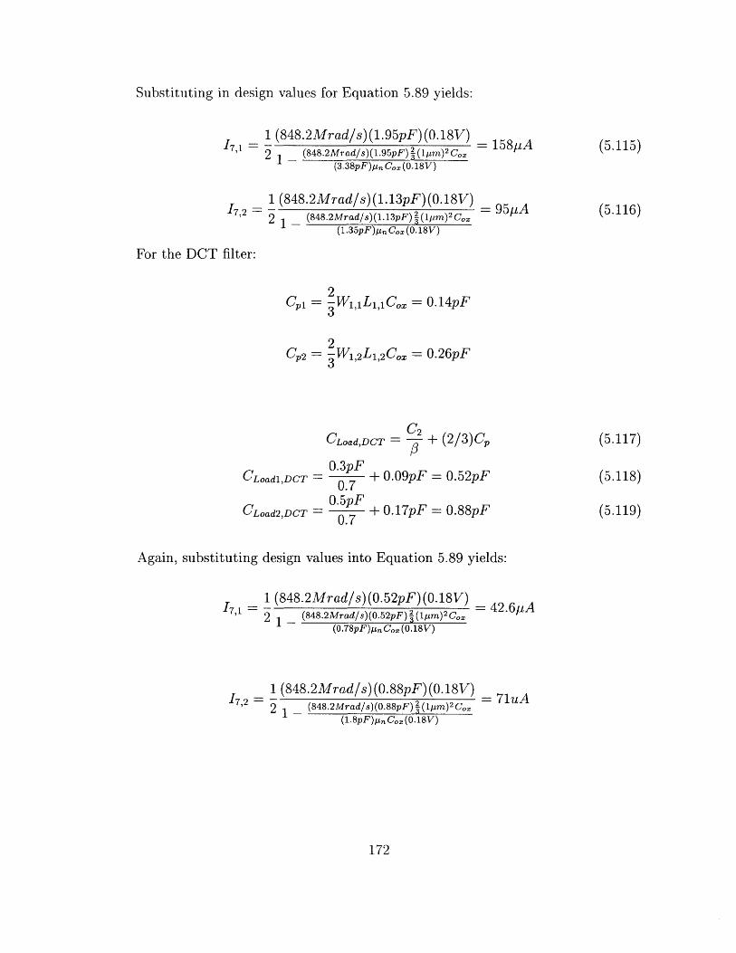
Substituting in design values for Equation 5.89 yields:
I7,1 ~1 (848.2Mrad/s) (1.95pF) (0.18V)2 1 (848.2Mrad/s)(1.95pF) j(bIm)2Cox
(3.38pF)pa Cox (0.18V)
1 (848.2Mrad/s)(1.13pF)(0.18V)2 1 (848.2Mrad/s)(1.13pF) 2 (1pm) 2
C,.,(1.35pF)p. C,. (0.18V)
For the DCT filter:
CPi = 2 W1,1L1,1Cox = 0.14pF3
C2= 2 Wl2,2o= 0.26pF
C2CLoad,DCT = + (2/3)Cp
CLoadl,DCT =
CLoad2,DCT
0. + 0.09pF = 0.52pF0.7
0.5p + 0.1 7pF = 0.88pF
Again, substituting design values into Equation 5.89 yields:
117,1 -
z
17,2
( _848.2Mrad/s)(0.52pF) (1m)C(0.78pF)1 , C,, (0.18V)
1 (848.2Mrad/s) (0.88pF) (0. 18V)2 1 (848.2Mrad/s)(0.88pF) 2(1pm)2Co
(1.8pF)pnCx(0.18V )
172
(848.2Mrad/s)(0.52pF)(0.18V)
158pA
= 95pA
(5.115)
(5.116)
(5.117)
(5.118)
(5.119)
=42.6 pA
= 71'uA
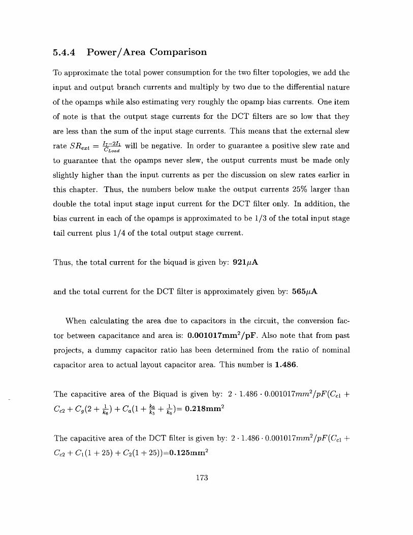
5.4.4 Power/Area Comparison
To approximate the total power consumption for the two filter topologies, we add the
input and output branch currents and multiply by two due to the differential nature
of the opamps while also estimating very roughly the opamp bias currents. One item
of note is that the output stage currents for the DCT filters are so low that they
are less than the sum of the input stage currents. This means that the external slew
rate SRext - 1--211 will be negative. In order to guarantee a positive slew rate andCLoad
to guarantee that the opamps never slew, the output currents must be made only
slightly higher than the input currents as per the discussion on slew rates earlier in
this chapter. Thus, the numbers below make the output currents 25% larger than
double the total input stage input current for the DCT filter only. In addition, the
bias current in each of the opamps is approximated to be 1/3 of the total input stage
tail current plus 1/4 of the total output stage current.
Thus, the total current for the biquad is given by: 921pA
and the total current for the DCT filter is approximately given by: 565piA
When calculating the area due to capacitors in the circuit, the conversion fac-
tor between capacitance and area is: 0.001017mm 2 /pF. Also note that from past
projects, a dummy capacitor ratio has been determined from the ratio of nominal
capacitor area to actual layout capacitor area. This number is 1.486.
The capacitive area of the Biquad is given by: 2 - 1.486 - 0.001017mm2 /pF(Cci +
Cc2 + Cg(2 + -) + Ca(1 + - + -)= 0.218mm 2
The capacitive area of the DCT filter is given by: 2. 1.486 . 0.001017mm2 /pF(Cc1 +
CC2 + C 1(1 + 25) + C2(1 + 25))=0.125mm 2
173
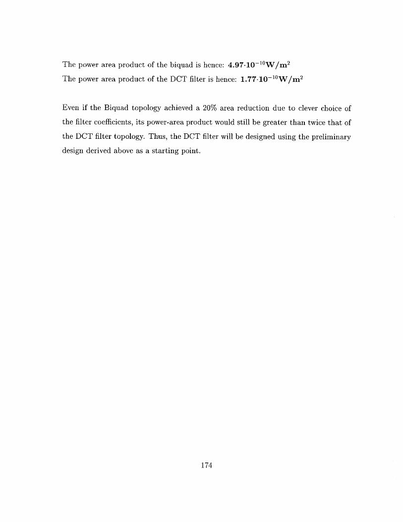
The power area product of the biquad is hence: 4.97-10- 1 0 W/m 2
The power area product of the DCT filter is hence: 1.77-10-1 0 W/m 2
Even if the Biquad topology achieved a 20% area reduction due to clever choice of
the filter coefficients, its power-area product would still be greater than twice that of
the DCT filter topology. Thus, the DCT filter will be designed using the preliminary
design derived above as a starting point.
174
Chapter 6
Analog Postfilter Implementation
and Simulation Results
The Direct Charge Transfer filter designed using the methods described in the pre-
vious chapter was implemented and simulated in a 0.25pm CMOS process in the
Cadence/Spectre design environment.
6.1 Analog Implementation
The full implementation of the postfilter, shown in Fig. 6-1, contains a number of
details not discussed in the previous chapter that are considered below. A hand
drawing of the schematic, with opamp and switch designations, is shown in Fig. 6-2
for clarity.
6.1.1 Architectural Considerations
Voltage References
For maximum voltage swing, the 2.5V supply rail can be used as the analog reference
voltage and is so used in this implementation. Since opamps in general have a good
175
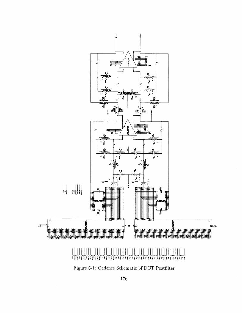
- - i~.
4L -~A ~v -_
i~i~
L i~j 2L.*iT
tiff1~
Figr Iaence S
Figure 6-1: Cadence Schematic of DCT Postfilter
176
11111111I I 1~t~tj
I
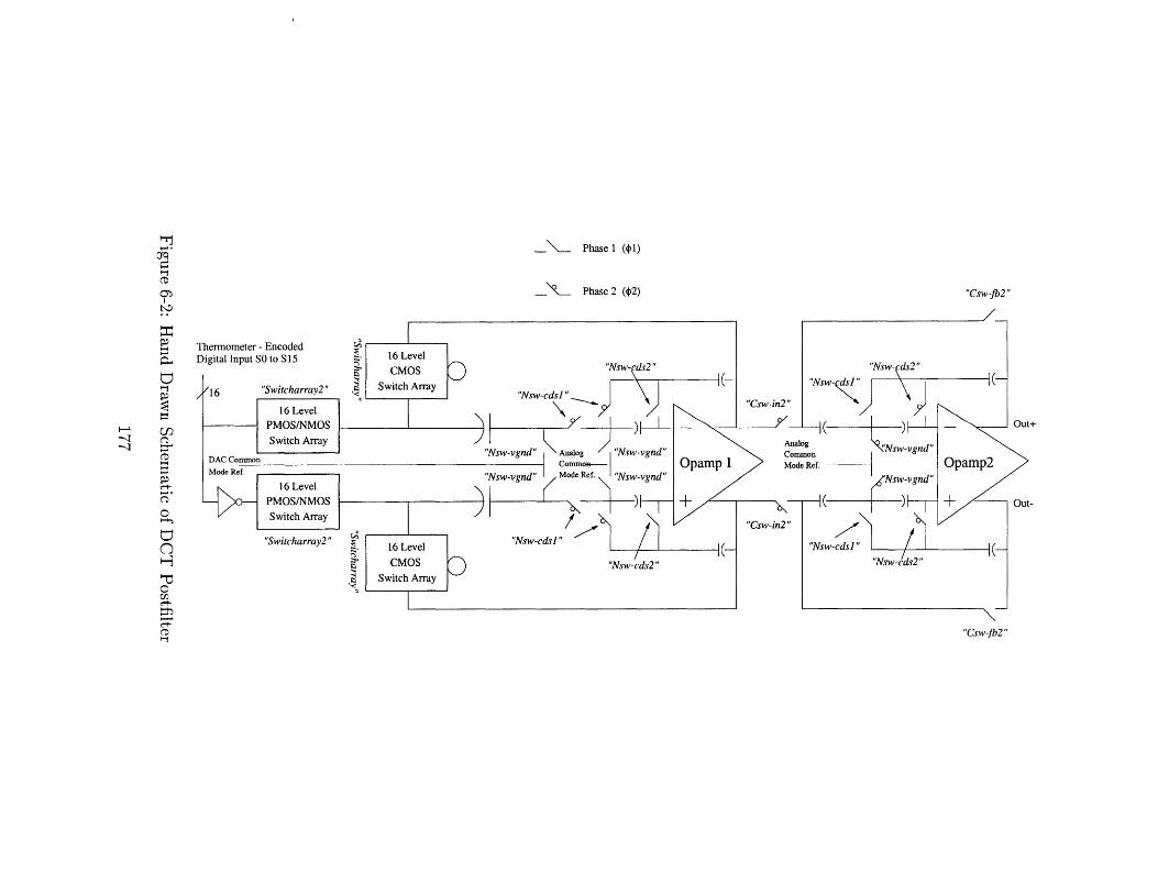
-\ Phase 1 ($l)
Phase 2 ($2)
hermometer - Encodedigital Input SO to S15 N. 16 Level
r CMOS "Nsw- ds2"
'16 "Switcharray2" Switch Array "Nsw-cd
16 LevelPMOS/NMOSSwitch Array
"Nsw-vgnd" Analog "Nsw-vgnd"DAC Common CommonMode Ref. "Nsw-vgnd" Mode Ref. "Nsw-vgnd"
16 LevelPMOS/NMOSSwitch Array
"Switcharray2" i "Nsw-cdsl"~. 16 LevelCMOS "Nsw-cds2"
2 Switch Array
-in
Opamp 1
"Csw-in
"Nsw- dsl
2"
-- ( _AnalogCommonMode Ref.
2
"Nsw-cdsl
"Csw-fb2"
"Nsw- ds2"
Out+
"Nsw-vgnd"Opamp2
Nsw-vgnd"
+ Out-
"Nsw-cds2"
"Csw-1b2"
o~.
CD
TD
tz)
CD
0
0
e+
0
"1Csw
power supply rejection ratio (PSRR), noise on this supply line generally has negligible
effect on the circuit. However, the same cannot be said of the reference for the D/A
converter. Any noise or spurious signals on the D/A reference couple directly into
the signal path, giving an effective PSRR of unity.
While previous DCT postfilter implementations solved this problem by bringing
a voltage reference from off-chip [17], such a strategy is disadvantageous for a fully
monolithic solution. Thus, an on-chip reference is used. Although the design of this
voltage reference is beyond the scope of this thesis, it can be said that in general, the
lower the value of the on-chip reference voltage, the greater amount of buffering can
be applied and the lower the noise on this line can be achieved. It was found from
previous implementations that an acceptable value for the digital reference voltage
was 2V, which resulted in a supply noise power of 8.55-10- 6 Vrms.
Since the postfilter implementation is fully differential, common mode reference
voltages are necessary to act as differential ground voltages. The digital common
mode reference is thus 1V and the analog common mode reference is 1.25V.
Dual Reference Switching Scheme
The astute reader will note that the switching scheme for the first DCT filter block
is somewhat different than that described in the previous chapter. The situation re-
quiring this switching setup is unique to the differential CDS-enhanced DCT filter.
Assume for a moment that the D/A capacitor array shared a common mode reference
voltage with the CDS capacitor. The common mode reference at this point would
have to be the digital reference, otherwise a voltage offset would exist between the
two differential signal paths. For the sake of argument, also assume that a DC input
of IV is introduced to the D/A sampling array (that is, 8 capacitors sample 2V,
while the other 8 sample OV). If this is the case, then the feedback capacitor must
178
have approximately no charge on it at DC. Also note that the opamp common mode
feedback constrains the output voltage at both opamps to be 1.25V in this condition.
Thus, on the first stage sampling clock phase <Di, the opposite terminal of the feed-
back capacitor is also at 1.25V and the CDS capacitors sample 0.25V plus any error
voltage at the opamp inputs. This represents a problem in that on the integrating
phase of operation, (D2, the voltage across the feedback capacitor is still OV. When its
bottommost terminal (as drawn) connects to the bottommost terminal of the CDS
capacitor, the DC voltages at the input terminals jump abruptly to 1.5V due to the
0.25V offset stored on the CDS capacitor. Such a jump at the input terminals causes a
temporary slewing in the common mode response of the opamp and must be avoided.
The solution is to split the two references with a switch that is open on <D1 and closed
on the integrating phase 4D2, at which time it is only the voltages across the CDS and
sampling capacitors that are of import.
Although not apparently obvious, the input terminals of the opamp start at OV
from circuit power up and eventually must reach 1.25V. This happens relatively
quickly through the same mechanism as described above. The initial voltage on
the feedback capacitor is 1.25V, since the common mode feedback holds the opamp
outputs at this level for a differential input of OV. Assuming for a moment that the
input voltage ramps of the opamps ramps up much faster than the filter input signal,
a DC differential input voltage to the D/A converter will result in that differential
voltage being stored across the sampling capacitors. After enough charge sharing
operations, this voltage appears across the feedback capacitor as well. As long as
the common mode feedback is working, this compels the bottommost terminals of
the capacitors to sit at 1.25V, as the differential output voltage appears on the top-
most capacitor terminals. Likewise, the opamp input terminals must also sit at 1.25V.
179
D/A Converter
The oversize capacitors and large switches at the bottom of Fig. 6-1 and Fig. 6-2
are high-level representations of the 16-capacitor array and its associated switches
that comprise the 4-bit D/A converter. At the very bottom of the figure are the
switch signals from the DWA circuitry. The timing diagram for these signals is
shown in Fig. 6-5. The switches in the bottommost blocks are comprised of single
PMOS and NMOS transistors in parallel. The PMOS transistors connect to the
high digital voltage reference of 2V, while the NMOS transistors connect to the low
voltage reference of OV. These switches were sized only as large as they needed to be
to guarantee complete settling of the reference voltage onto the sampling capacitor/
D/A element. The smaller blocks represent the arrays of switches that connect the
16 capacitors in parallel with the feedback capacitor. Since the voltages seen by these
switches are not binary, CMOS switches must be used and sized only large enough
to not affect the settling behavior of the opamp.
Common Mode Feedback
The common mode output of a differential opamp is not inherently set by the internal
biasing. Hence, an external common mode feedback circuit is required to keep the
output common mode voltage with an analog common mode voltage reference. The
process begins by averaging the two output voltages using a circuit as shown in Fig.
6-3.
When using switched-capacitors to implement a filter, the clocking infrastructure
is already present to implement a switched-capacitor common mode feedback circuit.
The switched capacitor common mode feedback presented in [46] and shown in Fig.
6-3 realizes an RC-equivalent averaging circuit with a very large time constant, thus
removing all but the lowest frequency components of the output common mode volt-
age.
180
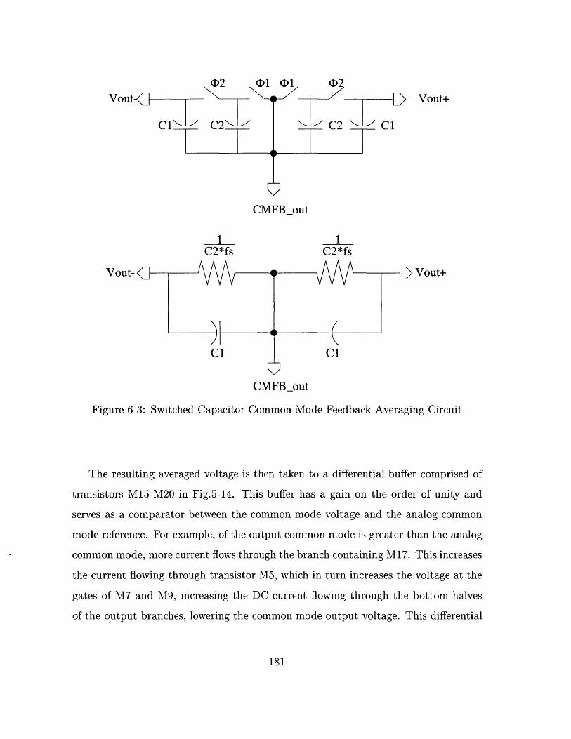
(D2 D1 (D1Vout-< L Vout+
Cl C2 C2 C1
CMFBout
1C2*fs
Vout-
Cl
1C2*fs
Vout+
C1
0CMFBout
Figure 6-3: Switched-Capacitor Common Mode Feedback Averaging Circuit
The resulting averaged voltage is then taken to a differential buffer comprised of
transistors M15-M20 in Fig.5-14. This buffer has a gain on the order of unity and
serves as a comparator between the common mode voltage and the analog common
mode reference. For example, of the output common mode is greater than the analog
common mode, more current flows through the branch containing M17. This increases
the current flowing through transistor M5, which in turn increases the voltage at the
gates of M7 and M9, increasing the DC current flowing through the bottom halves
of the output branches, lowering the common mode output voltage. This differential
181
buffer is used to increase the common mode feedback loop gain and to prevent capac-
itive loading of the switched-capacitor averaging circuit with the gate of M5. This
topology for a common mode feedback circuit also allows for greater design flexibility
and a larger output swing than other CMFB averaging circuits. [47]
6.1.2 Opamp Device Sizing and DC Operating Point
As shown in Table 6.1 and Table 6.2, the sizing of the key transistors (M1-M9) of the
opamp follows from the analysis given in Chapter 5. Some of the device sizes have
been changed slightly such that the simulated overdrive voltages match those given in
the aforementioned analysis. The output stage current in opamp 1 was also increased
slightly in order to doubly ensure that the external slew rate was of reasonable mag-
nitude. The compensation capacitor for opamp 1 was 0.8pF, while the compensation
capacitor for opamp 2 was 1.5pF.
Two-stage amplifiers such as the ones used in this design typically utilize lead
compensation in order to avoid a right-half plane zero resulting from the feedforward
path of a lone capacitor. Transistors M11 and M10 realize the resistors in the lead
network and were sized such that optimal settling occurred for the cold, slow process
corners. In general, a good starting point for iterating the resistance of this transistor
is to first size and bias it such that R = 1 [3]. This transistor was biased using the
temperature and process independent biasing scheme of M12-M14 that is described
in the Johns & Martin textbook [3].
The common mode feedback buffer transistors and the capacitors of the common
mode feedback circuit are designed to give an open loop gain of about 100, with suf-
ficient bandwidth and phase margin to allow the common mode to settle to an error
value of 1/100 before the end of the switching phase. The goal here is not extreme
182
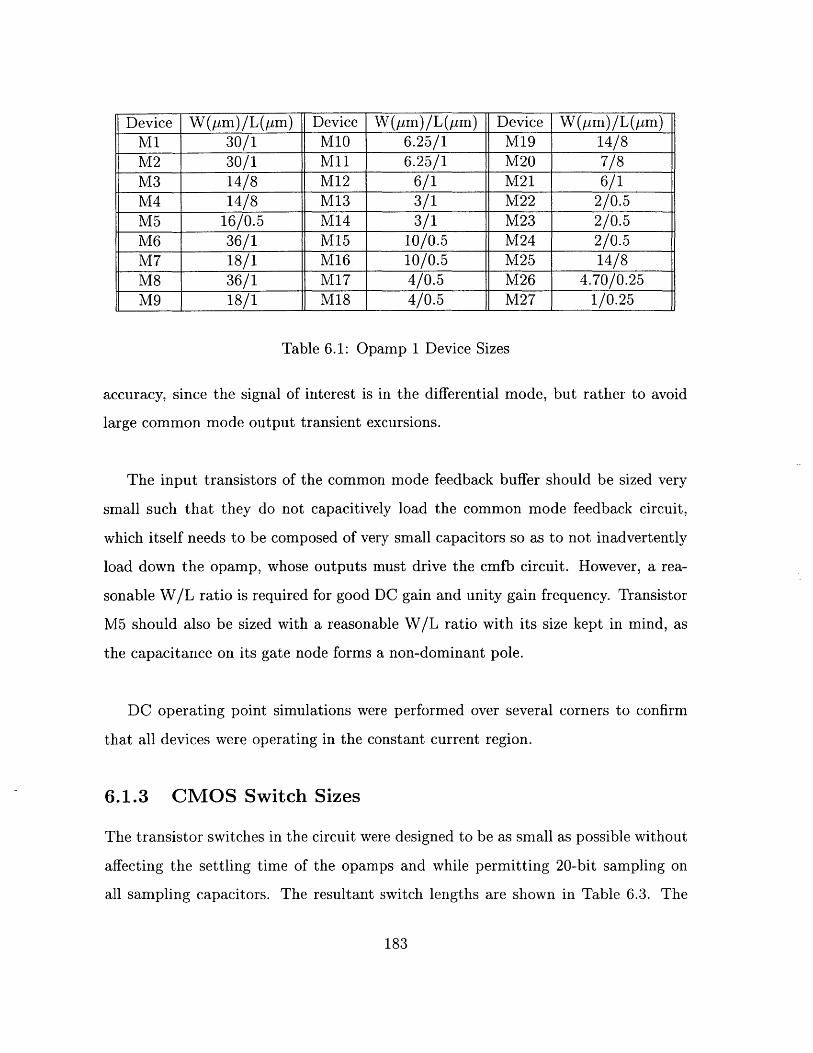
Device W(pm)/L(pm) Device W(pm)/L(pm) Device W(pm)/L(pm)Ml 30/1 M10 6.25/1 M19 14/8M2 30/1 M1l 6.25/1 M20 7/8M3 14/8 M12 6/1 M21 6/1M4 14/8 M13 3/1 M22 2/0.5M5 16/0.5 M14 3/1 M23 2/0.5M6 36/1 M15 10/0.5 M24 2/0.5M7 18/1 M16 10/0.5 M25 14/8M8 36/1 M17 4/0.5 M26 4.70/0.25M9 18/1 M18 4/0.5 M27 1/0.25
Table 6.1: Opamp 1 Device Sizes
accuracy, since the signal of interest is in the differential mode, but rather to avoid
large common mode output transient excursions.
The input transistors of the common mode feedback buffer should be sized very
small such that they do not capacitively load the common mode feedback circuit,
which itself needs to be composed of very small capacitors so as to not inadvertently
load down the opamp, whose outputs must drive the cmfb circuit. However, a rea-
sonable W/L ratio is required for good DC gain and unity gain frequency. Transistor
M5 should also be sized with a reasonable W/L ratio with its size kept in mind, as
the capacitance on its gate node forms a non-dominant pole.
DC operating point simulations were performed over several corners to confirm
that all devices were operating in the constant current region.
6.1.3 CMOS Switch Sizes
The transistor switches in the circuit were designed to be as small as possible without
affecting the settling time of the opamps and while permitting 20-bit sampling on
all sampling capacitors. The resultant switch lengths are shown in Table 6.3. The
183
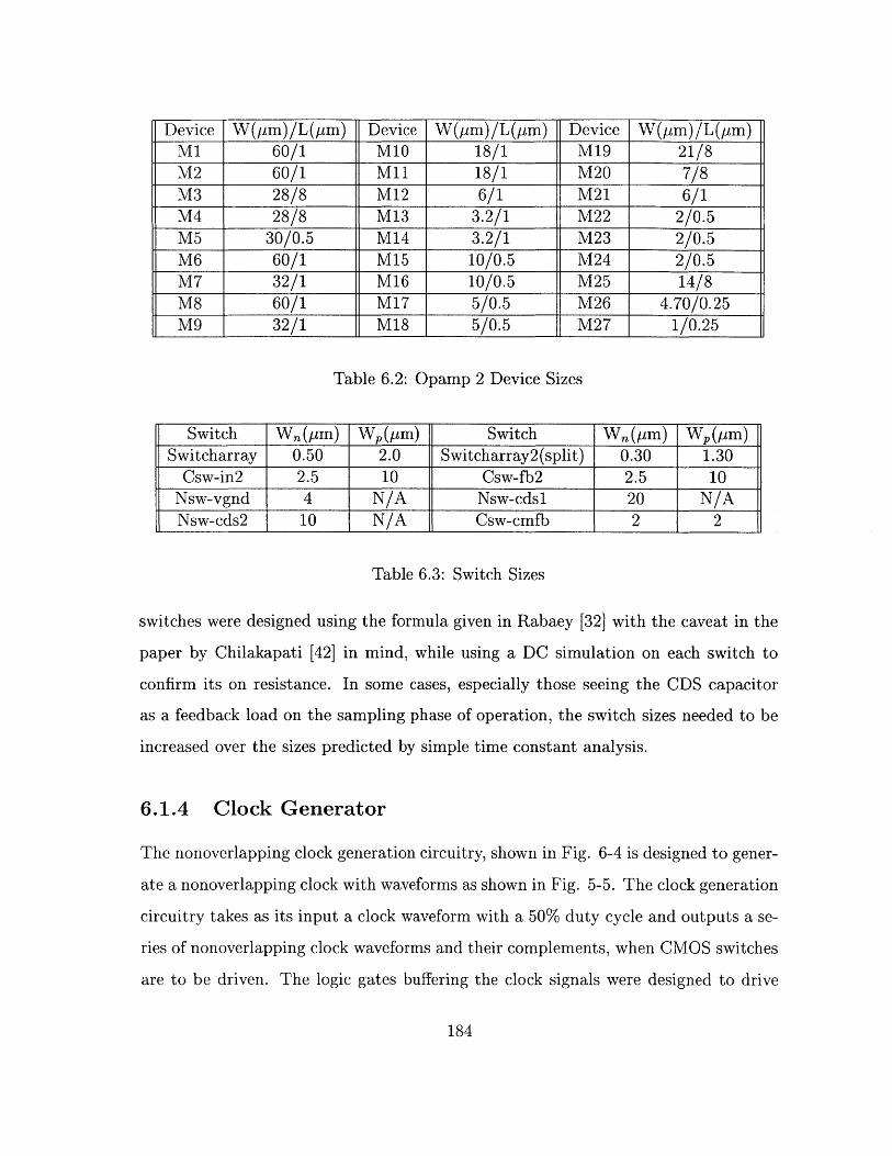
Device W(pm)/L(pm) Device W(pm)/L(pm) Device W(pm)/L(pm)M1 60/1 M10 18/1 M19 21/8M2 60/1 M1l 18/1 M20 7/8M3 28/8 M12 6/1 M21 6/1M4 28/8 M13 3.2/1 M22 2/0.5M5 30/0.5 M14 3.2/1 M23 2/0.5M6 60/1 M15 10/0.5 M24 2/0.5M7 32/1 M16 10/0.5 M25 14/8M8 60/1 M17 5/0.5 M26 4.70/0.25M9 32/1 M18 5/0.5 M27 1/0.25
Table 6.2: Opamp 2 Device Sizes
Switch Wn(Am) W,(Pm) Switch Wn(pm) W,(pm)Switcharray 0.50 2.0 Switcharray2(split) 0.30 1.30
Csw-in2 2.5 10 Csw-fb2 2.5 10Nsw-vgnd 4 N/A Nsw-cdsl 20 N/ANsw-cds2 10 N/A Csw-cmfb 2 2
Table 6.3: Switch Sizes
switches were designed using the formula given in Rabaey [32] with the caveat in the
paper by Chilakapati [42] in mind, while using a DC simulation on each switch to
confirm its on resistance. In some cases, especially those seeing the CDS capacitor
as a feedback load on the sampling phase of operation, the switch sizes needed to be
increased over the sizes predicted by simple time constant analysis.
6.1.4 Clock Generator
The nonoverlapping clock generation circuitry, shown in Fig. 6-4 is designed to gener-
ate a nonoverlapping clock with waveforms as shown in Fig. 5-5. The clock generation
circuitry takes as its input a clock waveform with a 50% duty cycle and outputs a se-
ries of nonoverlapping clock waveforms and their complements, when CMOS switches
are to be driven. The logic gates buffering the clock signals were designed to drive
184
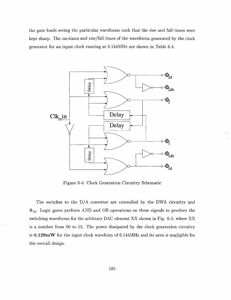
the gate loads seeing the particular waveforms such that the rise and fall times were
kept sharp. The on-times and rise/fall times of the waveforms generated by the clock
generator for an input clock running at 6.144MHz are shown in Table 6.4.
%db
Clk in Delay
Delay-
>0 1db
Id
Figure 6-4: Clock Generation Circuitry Schematic
The switches to the D/A converter are controlled by the DWA circuitry and
I>1d. Logic gates perform AND and OR operations on these signals to produce the
switching waveforms for the arbitrary DAC element XX shown in Fig. 6-5, where XX
is a number from 00 to 15. The power dissipated by the clock generation circuitry
is 0.129mW for the input clock waveform of 6.144MHz and its area is negligible for
the overall design.
185
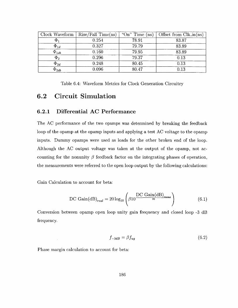
Clock Waveform Rise/Fall Time(ns) "On" Time (ns) Offset from Clk-in(ns)0.254 78.91 83.87
1I 0.327 79.79 83.894 11D 0.160 79.95 83.89
2 0.296 79.37 0.13_ 2_ 0.248 80.45 0.13
(D2db 0.096 80.47 0.13
Table 6.4: Waveform Metrics for Clock Generation Circuitry
6.2 Circuit Simulation
6.2.1 Differential AC Performance
The AC performance of the two opamps was determined by breaking the feedback
loop of the opamp at the opamp inputs and applying a test AC voltage to the opamp
inputs. Dummy opamps were used as loads for the other broken end of the loop.
Although the AC output voltage was taken at the output of the opamp, not ac-
counting for the nonunity 3 feedback factor on the integrating phases of operation,
the measurements were referred to the open loop output by the following calculations:
Gain Calculation to account for beta:
DC Gain(dB)DC Gain(dB),,,, = 20 logio ( 10 20 '" (6.1)
Conversion between opamp open loop unity gain frequency and closed loop -3 dB
frequency.
f-3dB ~ fug (6.2)
Phase margin calculation to account for beta:
186
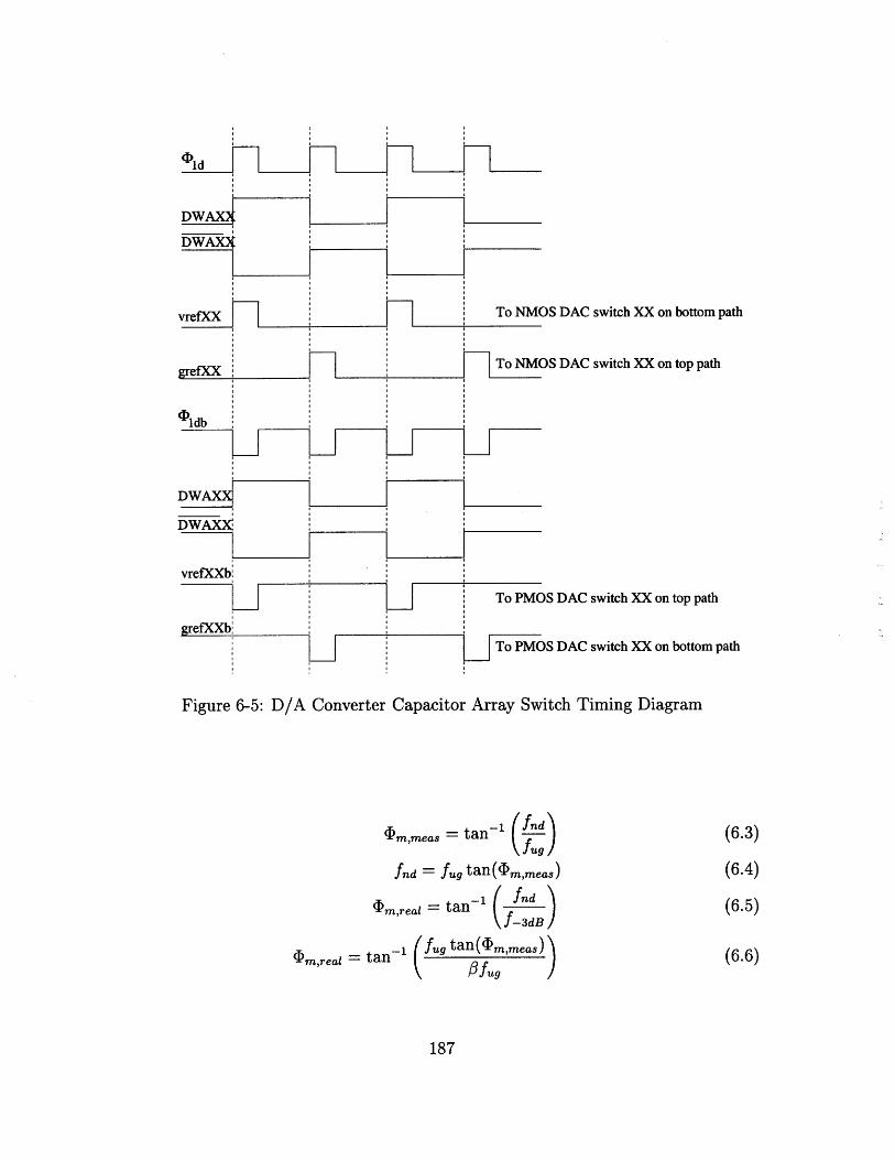
DWADWAX
vrefXX To NMOS DAC switch XX on bottom path
grefXX _To NMOS DAC switch XX on top path
Oldb
DWAXX,.
DWAX-
vrefXXb:
To PMOS DAC switch XX on top path
grefXXb_To PMOS DAC switch XX on bottom path
Figure 6-5: D/A Converter Capacitor Array Switch Timing Diagram
(m,meas = tan~ (ug (6.3)1u ('
fnAd = f tan(cl m,meas) (6.4)
45m,real = tan 1 ( fnd (6.5)\f-3dB
4)m,real = tan-1 fug tan(4Pm,meas) (6.6)
187
Clock Phase/Process Corner L 3 dB(MHz) 4m(degrees) DC Gain(dB)411, Typical 45.37 78.11 89.85(D2, Typical 29.18 78.20 86.75
JD1, Slow, -40'C 34.48 82.54 91.584D2, Slow, -40'C 22.65 81.49 88.47<bi, Slow, 110'C 34.67 81.54 89.66(D2, Slow, 110'C 22.34 80.57 86.56
i1, Fast, 110 C 59.38 72.37 81.20<b2, Fast, 110 0 C 37.59 73.60 78.10
Table 6.5: AC Performance for Opamp 1, Beta=0.7 for Phase 2
Clock Phase/Process Corner f 3dB(MHz) @m(degrees) DC Gain(dB)<D1 , Typical 29.97 82.08 86.30(D2, Typical 43.47 71.59 89.91
<bi, Slow, -400 C 22.76 85.06 88.044D2, Slow, -400 C 33.11 75.69 91.654i, Slow, 110*C 22.66 84.39 86.09(D2, Slow, 110'C 32.72 75.00 89.704b1, Fast, 110 0C 39.34 78.15 77.084b2, Fast, 1100 C 56.69 66.33 80.69
Table 6.6: AC Performance for Opamp 2, Beta=0.66 for Phase 1
Dmreal =tan1 (tan(Mmrneas)) (6.7)
Note that although the unity gain frequency of the opamps is slightly lower than
that called for by the analysis given in Chapter 4 for the worst-case corners, the
settling specifications were still met. In addition, it was found that a phase margin
slightly higher than 750 produced an optimal settling time for this implementation.
AC performance was also determined while sweeping the DC output differential
mode voltage to ensure that key AC parameters do not deviate into unacceptable
values as the filter signal waveform approaches its extremes. The results of these
188
simulations are shown in Figs. 6-6 and 6-7. Note that these plots are for the inte-
grating phases of both opamps, measured at the opamp outputs, and thus the plots
should be viewed with the 3 conversions described above in mind. However, the
key impetus behind the simulation is not lost, that is, the measurements still show
minimal deviation of phase margin and -3 dB frequency (related to GBW plot by
1/#) over the output differential mode range. DC Gain drop across the maximum
differential output mode range (OV to 0.8125V) in Figs. 6-6 and 6-7 is 3.59dB for
opamp 1 and 3.86dB for opamp 2 for the typical process corner. These numbers are
viewed as good indicators that the total harmonic distortion of the filter will be lower
than -60dB. Although the deviation for the hot, fast process corner is greater, this is
viewed as acceptable as the total harmonic distortion is specified only for the nominal
case. Note that in Fig. 6-6, the y-axis of the top graph in is units of Hz and the
y-axis of the center graph is in units of Degrees. In Fig. 6-7, the y-axis of the cen-
ter graph in is units of Degrees and the y-axis of the bottom graph is in units of Hz.
OTA Metrics for OTA1, Phase 2
GW(-40C'slow) -: GBW(25C,typ)
70M *: G 0 iCtost)
60M[____________________________________
PM 0C f ) -: PM(25C.typ)P10 fst)
DC Gain 40C slow) -: DC Goin(25Ctyp)DC Gorin( lOCtast)
.. .20 .40 .60 .80 1.0
Figure 6-6: AC Performance for Opamp 1 Swept Over Differential Output Swing
189
50M
40M
30M
79.0
76.0
73.0
70.0
67.0
100
90.0
80.0
70.0
60.0
50.0
OTA 2 Corner Performance
.: DC Gain (110C,fost) -: DC Goin(25Ctyp)
100 .': DC Goin(-40C,slow)
90.0
80.0
070.0
60.0
50.0 , . . . . . _ _ - -
4: PM(-40C,slow) PM(25C,typ)
79.0 -0: PM (110C,fast)
76.0
73.0
70.0
6 7 .0 ....... ....... ... .............
: GBW (-40C cold) GBW(25C,typ)70M -a: GBW(110oC,fst)
60M
50M
40M
30M _ _ _ _......._ ..... _..
0.0 .20 .40 .60 .80 1.0
Figure 6-7: AC Performance for Opamp 2 Swept Over Differential Output Swing
6.2.2 Common Mode Feedback Loop AC Performance
The AC Performance of the common mode feedback loop was determined by breaking
the feedback loop between the CMFB switched-capacitor averaging circuit and the
CMFB buffer inside the opamp. Since the CMFB circuit cannot maintain the common
mode output voltage during an AC simulation during which the CMFB loop is broken,
the output voltages of the opamps were set by ideal CMFB circuits outside of the test
schematic. A non-functional opamp serves as a dummy load here as in the differential
AC performance tests.
190
Clock Phase/Process Corner GBW(MHz) <>m(degrees) DC Gain(dB)I, Typical 42.39 71.92 38.16
4)2, Typical 35.89 65.60 40.19<D1 , Slow, -40'C 28.59 80.32 37.57<b2, Slow, -40'C 25.58 73.67 39.30i , Slow, 110,C 30.76 79.36 33.03
4)2, Slow, 110'C 26.77 72.42 34.734), Fast, 110 0C 60.93 60.36 37.87(D2, Fast, 110 0C 49.45 55.69 40.31
Table 6.7: AC-CMFB Performance for Opamp 1
Clock Phase/Process Corner GBW(MHz) <,m(degrees) DC Gain(dB)<bi, Typical 39.25 61.27 39.984<2, Typical 36.90 59.05 38.6
4D1, Slow, -40'C 28.18 68.37 39.41
<D2, Slow, -40 0 C 26.59 65.81 38.2341i, Slow, 110,C 27.94 68.44 34.13(D2, Slow, 110'C 26.20 65.74 32.97<bi, Fast, 110 0C 53.41 52.53 39.804D2 , Fast, 110 0C 50.25 51.01 38.12
Table 6.8: AC-CMFB Performance for Opamp 2
191
6.2.3 Transient Simulation Results
The effectiveness of the correlated double sampling circuitry was simulated by ap-
plying a sizing offset of 10% to the input transistor pair (M1-M2) and observing the
differential error voltage at the output of the filter for a DC filter input.
Output Differential Offset Without CDS: 10.7561mV
Output Differential Offset With CDS: 0.288mV
This represents an attenuation of -31.45dB at DC, enough to justify neglecting
input-referred 1/f noise from opamp 1. Note that this case was concocted purely
for test purposes and such a large sizing offset between the two input devices is not
expected over a typical process run.
The transient settling behavior of the opamps was determined for a worst-case
output voltage step. Since a simple observation of the sigma-delta modulator trans-
fer function shows at worst case, the input of the filter is incremented by only one D/A
converter level per clock cycle, the test was set up by generating both an increment
and a decrement of one level at the input of the filter. Note that this voltage step
is seen at the opamp outputs on the integrating phase of operation for both opamps
(<b2 for opamp 1 and b, for opamp 2). The input clock was slowed by a factor of
4 so that the true output voltage could be determined, then the difference between
this voltage and the actual output voltage at the end of the true time interval of (D2
(or 4D1) was taken and divided by the magnitude of the voltage step to ascertain the
error. The settling test results enumerated in Table 6.9 are for the worst case (high
or low) transition.
Although the settling resolution was slightly lower than 18 bits for the worst case
corner, it was decided that these results were acceptable for appropriate operation of
192
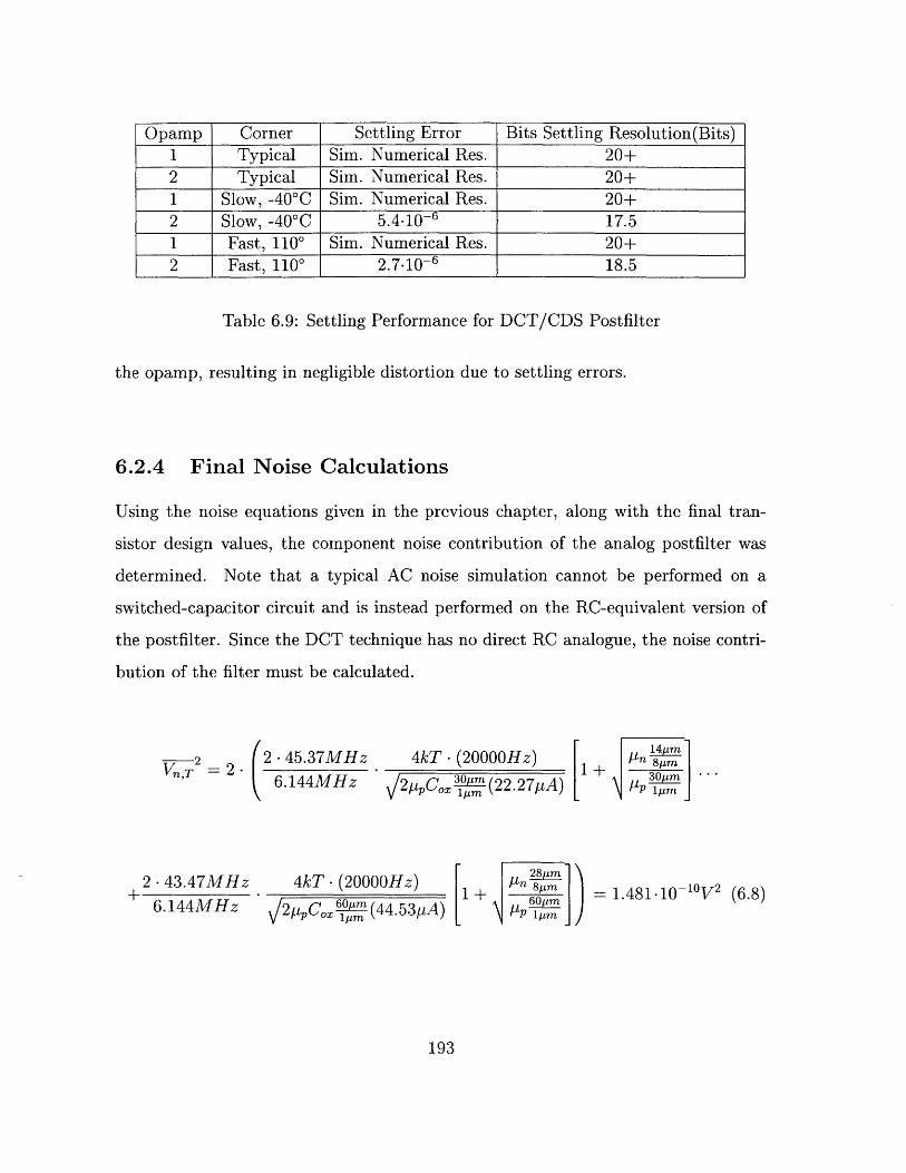
Opamp Corner Settling Error Bits Settling Resolution(Bits)1 Typical Sim. Numerical Res. 20+2 Typical Sim. Numerical Res. 20+1 Slow, -40'C Sim. Numerical Res. 20+2 Slow, -40 0C 5.4-10-6 17.51 Fast, 1100 Sim. Numerical Res. 20+2 Fast, 1100 2.7.10-6 18.5
Table 6.9: Settling Performance for DCT/CDS Postfilter
the opamp, resulting in negligible distortion due to settling errors.
6.2.4 Final Noise Calculations
Using the noise equations given in the previous chapter, along with the final tran-
sistor design values, the component noise contribution of the analog postfilter was
determined. Note that a typical AC noise simulation cannot be performed on a
switched-capacitor circuit and is instead performed on the RC-equivalent version of
the postfilter. Since the DCT technique has no direct RC analogue, the noise contri-
bution of the filter must be calculated.
2 2-45.37MHzV nT =2-
4kT- (20000Hz)
|2pCoxM ( 22.27 p A)
14pm
il+ 30pmL _~m j
2 -43.47MHz+ 6.144MHz
28jim14kT - (20000Hz) [ + n 8m
j2pCox llrn (44.53y A) 6 m ) = 1.481-10- 0 V 2 (6.8)
193
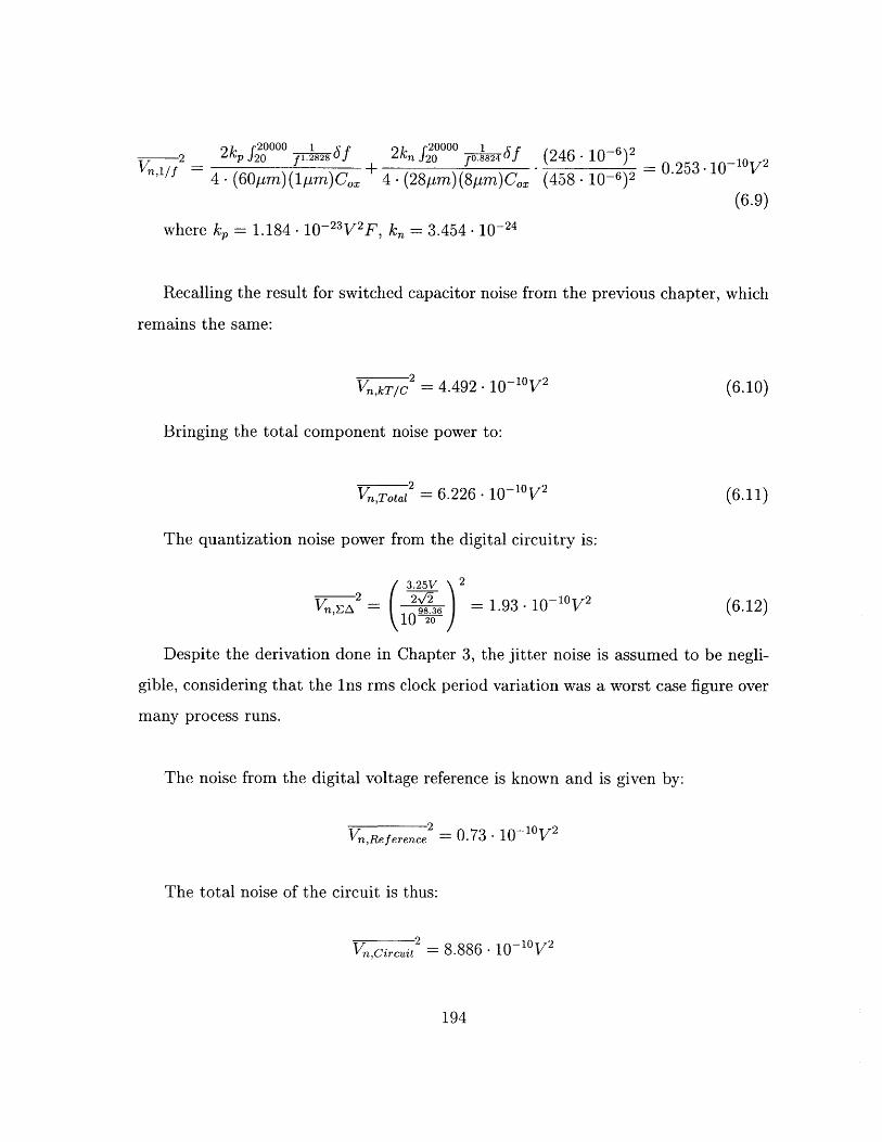
2 2k f fJooo i.28 28 6f 2kf f 00 po.8824 6f
',/f 4 - (60,pm)(Ipm)C, 4 - (28,pm)(8[pm)C,,,(246. 10-6)2 = 0.253 _-10~1V(458. 10-6)2
(6.9)
where kp = 1.184 - 10-23V 2F, kn = 3.454. 10-24
Recalling the result for switched capacitor noise from the previous chapter, which
remains the same:
Vn,kT/c2 = 4.492- 10-1OV2 (6.10)
Bringing the total component noise power to:
VnotOal2 = 6.226 - 10-10V2 (6.11)
The quantization noise power from the digital circuitry is:
Vn, A 2 (3.25V
2v83610 20
2
- 1.93. 10-10 V2 (6.12)
Despite the derivation done in Chapter 3, the jitter noise is assumed to be negli-
gible, considering that the Ins rms clock period variation was a worst case figure over
many process runs.
The noise from the digital voltage reference is known and is given by:
Vn,Reference 0.73- 1~V
The total noise of the circuit is thus:
Vn,Circuit = 8.886 i- 10 V2
194
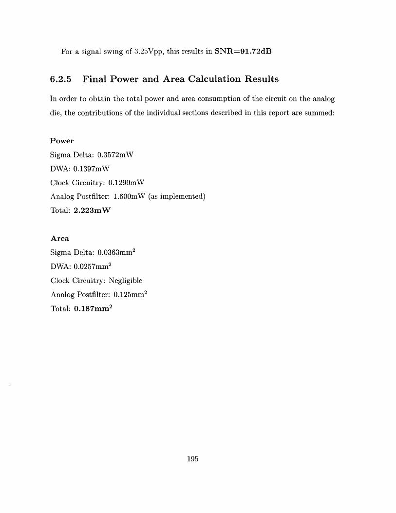
For a signal swing of 3.25Vpp, this results in SNR=91.72dB
6.2.5 Final Power and Area Calculation Results
In order to obtain the total power and area consumption of the circuit on the analog
die, the contributions of the individual sections described in this report are summed:
Power
Sigma Delta: 0.3572mW
DWA: 0.1397mW
Clock Circuitry: 0.1290mW
Analog Postfilter: 1.600mW (as implemented)
Total: 2.223mW
Area
Sigma Delta: 0.0363mm 2
DWA: 0.0257mm 2
Clock Circuitry: Negligible
Analog Postfilter: 0.125mm 2
Total: 0.187mm 2
195
Chapter 7
Conclusion
7.1 Summary
A low-power, low area oversampling converter for audio bandwidth applications has
been designed in a 0.25pm CMOS process. The previous discussion in this paper
centered on strategies and techniques to maximize the noise budget available to the
analog postfilter, where the area-power-noise tradeoff is severe. First, it was shown
that it was important to place major gain blocks in the D/A converter towards the
beginning of the chain. Second, it was shown that the number of stages in the digital
upsampling filter scheme must be minimized in order to avoid introducing in-band
quantization noise. Third, it was shown that a multibit sigma delta modulator run-
ning at a high oversampling ratio was necessary in order to guarantee the removal of
noise shaper quantization noise from the signal band.
A survey of several D/A converter topologies was then presented, describing the
merits and demerits for each. A brief analysis for each candidate architecture showed
that, given the objectives and requirements of this project, a switched-capacitor D/A
converter using dynamic element matching was best suited to achieve the noise spec-
ification with low power and area consumption. A brief summary of DEM techniques
196
was presented and the data weighted averaging (DWA) technique, a simple DEM
algorithm that also provides first-order mismatch noise shaping, was introduced.
The switched-capacitor technique known as Direct Charge Transfer was introduced
and examined, showing its robustness, parasitic insensitivity, noise performance, and
compatibility with autozeroing techniques that significantly reduce the 1/f opamp
noise. A hand design was performed in parallel on both a traditional biquad switched-
capacitor filter and a switched-capacitor DCT filter. It was shown that the for the
same noise performance, the DCT filter achieved a power-area product under half of
what a biquad filter could achieve.
Finally, transistor-level implementations of both the digital and analog circuitry
were designed and were shown to function properly over a range of process and tem-
perature corners.
7.2 Recommendations for Further Investigation
This section discusses a few areas of interest that are of relevance to this project, but
because of time constraints were left outside the scope of this document.
One item that deserves particular attention is the lack of an analog equivalent of
the DCT switched-capacitor technique. Whereas traditional switched-capacitor struc-
tures are well approximated as continuous-time resistors (either positive or negative)
provided that the oversampling ratio of the circuit is high enough, no such convenient
approximation exists for a DCT switching structure. As described previously, this
would simplify noise and AC transfer function analysis for the switched-capacitor
postfilter.
197
The DCT postfilter was also implemented as a cascade of two first-order sections,
resulting in two key disadvantages. First, such a cascade results in considerable pass-
band droop that must be compensated for elsewhere in the D/A converter chain,
most likely in the digital interpolation filters. Second, the filter does not have a high
pass transfer function from the inputs of the second opamp to the filter output. Since
the output of the second opamp cannot be sampled (it is the DT-CT interface), the
effectiveness of the correlated double sampling technique in rejecting opamp 1/f noise
is effectively halved. If a multiple-order DCT filter could be made to feed back to
previous stages, perhaps these two problems could be avoided while also enjoying the
power and area advantage provided by the DCT technique.
198
Bibliography
[1] H. Nyquist, "Certain Topics in Telegraph Transmission Theory," in AIEE Trans.,
pp. 617-644, 1928.
[2] M. Gustavsson, J. J. Wikner, and N. N. Tan, CMOS Data Converters for Com-
munications, Kluwer Academic Publishers, Boston, MA, 2000.
[3] D. A. Johns, K. Martin, Analog Integrated Circuit Design, John Wiley and Sons,
New York, 1997.
[4] A. V. Oppenheim, R. W. Schafer, and J. R. Buck, Discrete-Time Signal Process-
ing, 2nd Edition, Prentice Hall, Englewood Cliffs, NJ, 1998.
[5] K. Falakshahi, C-K.K.Yang, B.Wooley, "A 14-bit, 10-Msamples/s D/A Converter
Using Multibit Sigma-Delta Modulation," in IEEE J. of Solid State Circuits, vol.
34, pp. 607-615, May 1999.
[6] J. L. Gonzalez and E. L. Alarcon, "Clock-Jitter Induced Distortion in High Speed
CMOS Switched-Current Segmented Digital to Analog Converters," in IEEE
Symp. Circuits Systems, vol. 1, pp. 512-515, 2001.
[7] M. Shinagawa, Y. Azakawa, and T. Wakimoto, "Jitter Analysis of High-Speed
Sampling Systems," in IEEE J. of Solid State Circuits, vol. 25, pp. 220-224, Feb.
1990.
199
[8] M. Pelgrom, A. Duimmaijer, and A. Welbers, "Matching Properties of MOS tran-
sistors," in IEEE J. Solid State Circuits, vol. 24, pp. 1433-1439, October 1989.
[9] B. Blesser, "Digitization of audio: A comprehensive examination of theory, im-
plementation, and current practice," in J. Audio Eng. Society, vol. 26, no. 10, pp.
739-771, October 1978.
[10] W. Sansen and K. Laker, UC Berkeley Extension Class Notes, Fall 2001.
[11] W.R. Bennett, "Spectra of Quantized Signals," in Bell System Technical J.
vol.27, pp. 446-472, 1948.
[12] K. Nguyen, R. Adams, and K. Sweetland, "A 113dB SNR Oversampling Sigma-
Delta DAC for CD/DVD Application," in IEEE Trans. Consumer Electronics,
vol. 44, pp. 1019-1023, August 1998.
[13] S. Norsworthy, R. Schreier, and G. Temes, Delta-Sigma Data Converters, IEEE
Press, Piscataway, NJ, 1997.
[14] R.M. Gray, "Quantization Noise Spectra," in IEEE Trans. Information Theory,
vol.36, issue 6, pp. 1220-1244, November 1990.
[15] W.L. Lee and C. Sodini, "A Topology for Higher Order Interpolative Coders,"
in ISCAS Digest, pp. 459-462, 1987.
[16] D. Anastassiou, "Error Diffusion Coding for A/D Conversion," in IEEE Trans.
Circuits Systems, vol. 36, no. 9, pp. 1175-1186, September 1989.
[17] I. Fujimori and T. Sugimoto, "A Multibit Delta-Sigma Audio DAC with 120-dB
Dynamic Range," in IEEE J. Solid State Circuits, vol. 35, pp. 1066-1073, August
2000
[18] H.W. Paik and T.W. Grablander, "FIR Compensation Filter for the Zero Order
Hold D/A Converter Using the Frequency Sampling Method", in Proceedings of
the 37th Midwest Symposium on Circuits and Systems, vol. 2, pp. 1006-1009, 1994.
200
[19] T.W. Parks and J.H. McClellan, "A program for the Design of Linear Phase
Finite Impulse Response Filters," in IEEE Trans. Audio Electroacoustics, vol.
AU-20, no. 3, pp. 195-199, August 1972.
[20] J.F. Kaiser, "Nonrecursive Digital Filter Design Using the 10-Sinh Window Func-
tion," in IEEE Symp. on Circuits and Systems, vol. 1, pp. 20-23, April 1974.
[21] D. Wouter, J. Groeneveld, H.J. Schouwenaars, H.A.H. Termeer, and C.A.A.
Bastiaansen, "A Self-Calibration Technique for Monolithic High-Resolution D/A
Converters," in IEEE J. Solid State Circuits, vol. 24, pp. 1517-1522, December
1989.
[22] R. Baird and T. Fiez, "Linearity Enhancement of Multibit Delta-Sigma A/D and
D/A Converters Using Data Weighted Averaging," in IEEE Trans. on Circuits
and Systems - II Analog and digital Signal Processing, vol. 42, pp. 753-762
December 1995.
[23] T. Kwan, R. Adams, and R. Liebert, "A Stereo Multibit EA DAC with Asyn-
chronous Master-Clock Interface," in IEEE J. Solid-State Circuits, vol. 31, pp.
1881-1887, December 1996.
[24] P. Rombouts and L. Weyten, "A Study of Dynamic Element-Matching Tech-
niques for 3-Level Unit Elements," in IEEE Trans. on Circuits and Systems - II:
Analog and Digital Signal Processing, vol. 47, pp. 1177-1187, no. 11, November
2000.
[25] R.W.Gregor, "On the Relationship Between Topography and Transistor Match-
ing in an Analog CMOS Technology," in IEEE Trans. on Electron Devices vol.
39, no. 2, pp. 275-282, February 1992.
[26] D.K. Su and B.A. Wooley, "A CMOS Oversampling D/A Converter with a
Current-Mode Semidigital Reconstruction Filter," in IEEE J. Solid State Cir-
cuits, vol. 28, pp. 1224-1233, December 1993.
201
[27] L. Jackson, Digital Filters and Signal Processing, 2nd ed. Boston: Kluwer 1990.
[28] C.C. Enz and G.C. Temes, "Circuit Techniques for Reducing the Effects of Op-
amp Imperfections: Autozeroing, Correlated Double Sampling, and Chopper Sta-
bilization," in Proc. IEEE, vol. 84, pp. 1584-1614, November 1996.
[29] J.H. Fischer, "Noise Sources and Calculation Techniques for Switched Capacitor
Filters," IEEE J. Solid State Circuits, vol. SC-17, no. 1, pp. 742-752, August 1982.
[30] U-K.Moon, J.Silva, J.Steensgaard, and G.Temes, "A Switched-Capacitor DAC
with Analog Mismatch Correction," IEEE Symp. Circuits Systems, vol. 1, pp.
421-424, 2000.
[31] J. Steensgaard, U-K. Moon, G. Temes, "Mismatch-Shaped Pseudo-Passive Two-
Capacitor DAC," in Conference Proceedings for the 1999 IEEE Alessandro Volta
Workshop on Low Power Design (VOLTA '99), held March 4-5, 1999 in Como,
Italy
[32] J. Rabaey, Digital Integrated Circuits: A Design Perspective, 1st ed.,New Jersey:
Prentice Hall 1996.
[33] I. Fujimori and T. Sugimoto, "A 1.5V, 4.1mW dual-channel audio delta-sigma
D/A converter,"in IEEE J. Solid State Circuits, vol. 32, pp. 933-942, July 1997.
[34] P.W. Bosshart, "A Multiplexed Switched Capacitor Filter Bank," in IEEE J.
Solid State Circuits, vol. 15, pp. 939-945, December 1980.
[35] N.S. Sooch, J.W. Scott, T. Tanaka, T. Sugimoto, C. Kubomura, "18-b stereo
D/A Converter with Integrated Digital and Analog Filters," presented at the 91st
AES Convention, October 1991.
[36] O.J.A.P. Nys and R.K. Henderson, "An Analysis of Dynamic Element Matching
Techniques in Sigma-Delta Modulation," in IEEE Symp. Circuits Systems, vol. 1,
pp. 231-234, 1996.
202
[37] R. Radke, A. Eshraghi, and T. Fiez, "A 14-bit Current-Mode Sigma-Delta DAC
Based Upon Rotated Data Weighted Averaging," in IEEE J. of Solid State Cir-
cuits, vol. 35, pp. 1074-1084, August 2000.
[38] M. Vadipour, "Techniques for Preventing Tonal Behavior of Data Weighted Av-
eraging Algorithm in Sigma Delta Modulators," in IEEE Trans. on Circuits and
Systems II: Analog and Digital Signal Processing, vol. 47, no. 11, pp. 1137-1144,
November 2000.
[39] T. Shui, R. Schreier, and F. Hudson, "Mismatch Shaping for a Current-Mode
Multibit Delta-Sigma DAC,"in IEEE J. of Solid State Circuits, vol. 34, pp. 331-
338, March 1999.
[40] D. Su, "Oversampling Digital-to-Analog Conversion," Ph.D
ford Univ., August 1994.
[41] C.C. Enz and G. Temes, "Circuit Techniques for Reducing
Amp Imperfections," Proceedings of the IEEE, vol. 84, no.
November 1996.
[42] U. Chilakapati, T.S. Fiez, "Effect of Switch Resistance on
Settling Time," in IEEE Trans. Circuits Systems-II Analog
Processing, vol. 46, no. 6, pp. 810-816, June 1999.
dissertation, Stan-
the Effects of Op-
11, pp. 1584-1614,
the SC Integrator
and Digital Signal
[43] K. Martin, A.S.Sedra, "Effects of the Op Amp Finite Gain and Bandwidth on
the Performance of Switched-Capacitor Filters," in IEEE Trans. Circuits Systems,
Vol. CAS-28, pp. 822-829, August 1981.
[44] Y. Huang, G.C.Temes, P.F.Ferguson, "Reduced Nonlinear Distortion in Circuits
with Correlated Double Sampling," in IEEE Symp. Circuits and Systems, vol.1,
pp. 159-162, 1996.
203
[45] F. Wang, R. Harjani, "Power Analysis and Optimal Design of Opamps for Over-
sampled Converters," in IEEE Trans. Circuits Systems, vol. 46, pp. 359-369, April
1999.
[46] M. Sarhang-Nejad, G.C.Temes, "A High Resolution Multibit EA ADC with
Digital Correction and Relaxed Amplifier Requirements," in IEEE J. Solid-State
Circuits, vol. 28, no. 6, pp. 648-660, June 1993.
[47] H. Recoules, R. Bouchakour, P. Lourneau, "A Comparative Study of two SC-
CMFB networks used in fully differential OTA," in IEEE Int'l Conference on
Electronics, Circuits, and Systems, vol. 2, pp. 291-294, 1998.
[48] D.G.Haigh and B.Singh, "A Switching Scheme for Switched-Capacitor Filters
which Reduced the Effect of Parasitic Capacitances Associated with Switch Con-
trol Terminals, in IEEE Symp. Circuits Systems, vol. 1, pp. 586-589, May 1993.
[49] K. Laker and W. Sansen, Design of Analog Integrated Circuits and Systems,
McGraw Hill Publishers, 1994.
204