Embed Size (px)
Citation preview

Page 1 of 26
A DC OFFSET CONTROLLER FOR TRANSFORMERLESS SINGLE PHASE
PHOTOVOLTAIC GRID-CONNECTED INVERTERS
L. Bowtell and A. Ahfock
Abstract –
Limitation of DC injection into the AC network is an important operational requirement for grid-
connected photovoltaic systems. One way to ensure that this requirement is met is to use a power
transformer as interface to the AC network. But this adds costs, mass, volume and power losses. In
a transformerless system, the inverter forming part of the photovoltaic system has to be operated so
that DC content in its output current is below specified limits. Ideally there should be no DC at the
output of the inverter, but in practice, in the absence of special measures, a small amount of DC
current is present. A technique for elimination of the DC offset is proposed. It is based on the
sensing of the DC offset voltage at the output of the inverter. The sensor output is used to drive a
feedback system designed to control operation of the inverter so that the DC offset is forced to stay
within acceptable limits. A mathematical model for the DC offset controller is derived. A design
procedure, based on the model, is proposed for the controller. Results of tests performed on a system
of 1kW nominal rating, provides validation for the mathematical model.

Page 2 of 26
1. INTRODUCTION
Dispersed generation typically involves conversion from DC to AC. Grid-connected photovoltaic
(PV) systems, on which this paper focuses, are well-known examples. They require an inverter to
convert DC from solar panels to AC. Ideally the output current of the inverter will be purely AC,
but in practice, unless special measures are taken, it will contain a small amount of DC. Injection of
DC into the AC mains, if excessive, can lead to problems such as corrosion in underground
equipment [1], transformer saturation and transformer magnetising current distortion [2] and
malfunction of protective equipment [3]. Therefore guidelines and standards have been set up to
regulate DC injection [4]. For example Australian Standard AS4777.2 limits DC injection to 5mA or
0.5% of rated output whichever one is greater [5] and, in the United Kingdom, ER G83/1 imposes a
limit of 5mA [6].
The simplest way to eliminate DC injection is to include a grid frequency transformer. This has
been the solution adopted in a number of commercial systems [7, 8]. Inclusion of a grid frequency
transformer implies major disadvantages such as added cost, mass, volume and power losses. Some
commercial systems include a smaller higher frequency transformer or are transformerless [8].
Measurements of DC currents from the AC output of commercial systems are presented in
reference [8]. Compared to the limits imposed by AS4777.2 or by ER G83/1, the measured DC
currents were found to be very significant. Methods to solve the DC injection problem have been
proposed [1,9,10]. References [1] and [9] suggest the use of a feedback loop to eliminate the DC
offset in the inverter output. Reference [1] suggests using a voltage sensor at the inverter output
consisting of a differential amplifier and a low pass filter. Any DC detected at the output of the low
pass filter is fed back to the controller which in turn operates the inverter in such a way as to reduce
the DC offset. A simple mathematical model is suggested for the control system and it is assumed
that the inverter is voltage controlled. However, experimental results are not reported.

Page 3 of 26
Reference [9] considers a current controlled inverter. Again a sensor is connected at the output of
the inverter to detect any DC offset voltage. The sensor consists of an RC circuit and a 1:1 signal
transformer. It is recognised that the DC signal is of the order of less than a few mV and needs to
be extracted from a total signal of more than two hundred volts which is essentially the grid supply
voltage. The RC circuit is connected in series with the secondary side of the 1:1 signal transformer.
The series combination is connected across the inverter output. The primary side of the 1:1 signal
transformer is connected across the AC supply. Thus, if it is assumed that the signal transformer is
perfect and that the secondary voltage of the transformer opposes the AC supply voltage, only DC
appears across the capacitor in the RC branch. The capacitor voltage is fed back to the controller
which in turn adjusts the inverter current reference so that the DC offset is eliminated. No
quantitative experimental results are reported, except for a statement that the DC offset controller
has been found to operate correctly. A mathematical model of the controller is presented in a
subsequent paper [11]. The mathematical model is experimentally validated and it is shown that the
1:1 transformer is effective only if its primary winding time constant is sufficiently low. In other
words a relatively large core and a low winding resistance are necessary, making the DC offset
sensor bulky and expensive. The DC Offset controller proposed in reference [10] is based on
calibration of the DC link current sensor used for controlling the inverter output current. Software
ensures that current measurements made during freewheeling intervals are corrected to zero. This
technique is limited to unipolar switched inverters controlled in a manner where these freewheeling
intervals are easily determined.
In this paper a more cost effective DC offset sensor is proposed. Unlike references [1] and [9],
where DC sensing is carried out across the AC supply terminals, the DC offset sensor is connected
across the ripple filter inductors forming part of the LCL ripple filter. The disadvantage of sensing
across the AC supply terminals is that the sensed DC offset could be due to sources other than the

Page 4 of 26
inverter. On the other hand the DC offset detected by the proposed sensor is guaranteed to be
caused by the inverter being controlled. A design procedure is developed for the proposed DC
offset controller. The paper is also about investigating possible interactions between the DC offset
control loop and other control loops within the system.
2. System Overview
There are a number of system configurations that have been proposed for single phase grid-
connected photovoltaic (PV) systems [12]. The configuration that has been used to evaluate the DC
offset elimination method is shown in figure 1. One major advantage of the chosen configuration is
the use of a single-stage power electronic conversion. Power from the DC bus is converted to AC
by the inverter and fed into the AC network. The DC offset controller that is being proposed
represents an additional control loop for the grid-connected photovoltaic system. There are three
other control loops which are described below.
2.1 Inverter Switching
The main components of the inverter are shown in figure 2. As unity power factor is aimed for
reference current iref for the hysteretic current controller [12, 13] is arranged to be in phase with
AC supply voltage vs. During the positive half cycle of the source voltage, insulated gate bipolar
transistor TB+ is kept off and TB- is kept on. Transistor TA+ is switched on when the inverter output
current (i) goes below the bottom limit of the hysteretic band. This causes i to rise while it flows
through TA+ and TB- . When current i goes above the upper limit of the band TA+ is switched off.
This causes i to fall while it flows through DA- and TB-.

Page 5 of 26
During the negative half cycle of the ac supply voltage, transistor TB- is kept off and TB+ is kept on.
Transistor TA- is switched on when the inverter output current i goes above the top limit of the
hysteretic band. This causes current i to rise negatively while it flows through TB+ and TA- . When
current i goes outside the lower limit of the band TA- is switched off. This causes i to fall towards
zero while it flows through DA+ and TB+ . Typical inverter output current waveforms, unfiltered (i)
and filtered (is) are given in figure 3.
2.2 DC Bus Voltage Control
Since there is no substantial storage between the output of the solar panels and the output of the
inverter, there is a need for control of power. As the insolation level rises or falls, the rms value of
reference current iref should automatically rise or fall in proportion so that power balance is
preserved. It is the role of the voltage control loop to maintain balance between the DC output of
the PV array and the inverter output into the AC network.
As shown in figure 2, the DC bus voltage signal kcvc and the reference voltage kcvref are inputs to
the voltage controller. At steady state, if the controller uses integral action, the DC bus voltage
signal kcvc will be equal to the DC bus reference voltage kcvref and the controller output vce will be a
constant. The output of the voltage controller is multiplied with the mains AC voltage signal ksvs to
produce the current reference signal khiref. The inverter output current signal khis and the current
reference signal khiref are inputs to the hysteretic current controller which generates gate signals to
switch appropriate inverter devices as described in section 2.1.

Page 6 of 26
A rise in output power from the solar panels tends to cause a rise in DC bus voltage vc which in turn
causes a rise in vce. This causes Iref (rms of iref) to rise resulting in inverter output current Is (rms of
is) rising because it tracks Iref. The rise in current Is restores power balance between the DC power
output of the solar panels and the AC power output of the inverter. Thus the aim of the voltage
control loop is to maintain power balance by getting the DC bus voltage signal kcvc to be equal to
the reference voltage kcvref.
2.3 Maximum Power Tracker
The commonly used perturb and observe method [14] was selected for maximum power point
tracking. The maximum power tracker is a control loop in its own right. Whereas the voltage
control loop aims for balance between power output from the panels and power output by the
inverter, the maximum power tracker aims to operate the solar panels at a voltage level that allows
maximum extraction of power. The maximum power tracking routine was digitally implemented as
follows:
a) Calculate and record panel output power (vcip in figure 2);
b) Decrement the voltage reference by ∆v, where ∆v is a small value;
c) Wait a short time , about 2 to 3 seconds, to allow vc to settle to its new value;
d) Calculate ∆P, the change in panel output power compared to the value obtained in step(a)
e) Reverse the previous change in reference voltage if ∆P ≤ 0 otherwise change the
voltage reference by ∆v in the same direction as the previous change.
f) Repeat steps (a) to (e).

Page 7 of 26
2.4 DC Offset Controller
The DC offset sensor is made up of a double stage RC filter. The voltage across the ripple filter
inductors (vf) is sensed and filtered. The DC offset sensor relies on the finite value of resistance of
the ripple filter inductors L and Lr. If the DC component in the inverter current was constant, the
DC output voltage of the sensor would be equal to IR, where I is the DC component of current and
R is the resistance of the two series connected inductors. This voltage, labelled as vo in figures 2
and 4, is earth referenced and contains a relatively low level of AC due to the action of the double
stage RC filter. As shown in figure 4, the output of the filter is fed to a PI controller whose
reference input is equal to zero. The output of this controller adds to the signal from the DC bus
controller is such a way as to cause Vo , which is the mean value of vo, to come down to zero. The
integral action of the DC offset controller ensures that Vo is equal to zero at steady state.
The DC offset controller needs to be carefully designed. The main requirements are that:
(a) it should not interfere with the operation of the other control loops and vice-versa;
(b) its dynamic response must be acceptable.
3. MATHEMATICAL MODEL
Refer to figure 4 which is a block diagram representation of the DC offset sensor. The input to the
DC offset sensor is the voltage across the ripple filter inductors. This voltage is assumed to be
made up of two components. They are a fast changing component labelled as vL and a slow
changing component equal to (io-ic)R. The fast changing component would essentially be a mains
frequency sinusoidal signal equal to Lω is.

Page 8 of 26
τi
dv i
dtk p vo 0
τ f
dv0
dtv o v1
One part of the slow changing component is due to an unwanted DC offset current(io) which may be
present because of circuit imperfections. The other part is due to the compensating current ic which
is proportional to the output signal from the DC offset control loop. The reasonable assumption
made in figure 4 is that the slow changing component of inverter current contributes only a resistive
voltage to the input of the DC offset sensor. Similarly it is assumed that the fast changing
component of the inverter current contributes only an inductive voltage to the input of the DC offset
sensor. If io is constant at steady state, the PI controller ensures that ic is equal to io thus ensuring
the inverter output current is free of DC.
Referring to figure 2, for the second stage of the two-stage RC filter we have:
(1)
where τf = Rf C
Since node N in figure 2 is the neutral and an MEN(multiple earthed neutral) is assumed, the
current input into the first stage of the two-stage RC filter is given by:
(2)
which may be written as
(3)
where τf = Rf C
In figure 4, voltage vo is the input to the PI controller. The relationship between vo and the output of
the integral element is given by:
(4)
where τi = PI controller integration time constant and kp = proportional gain

Page 9 of 26
The output of the PI controller (khic) is given by:
khic = kpvo + vi (5)
From figure 4:
vf = vL + (io - ic)R (6)
Combining equations 1 to 6 and taking the Laplace transform results in equation 7. The constant k
in equation 7 is equal to R kp / kh.
(7)
In arriving at equation (7) coupling between the DC offset control loop and the other three control
loops have been ignored. This assumption of negligible coupling needs to be justified. Any
interaction between the maximum power tracker and the DC offset control loop would be through
the DC bulk storage capacitor voltage vc which is controlled by the DC bus voltage control loop. It
can be argued that there is practically zero coupling between the DC bus voltage control loop and
the DC offset control loop. The fundamental reason behind this is that the DC bus voltage control
loop is driven by the imbalance between DC power from the DC bus and AC power injected into
the AC network whereas the action of the DC offset controller has practically no effect on that
power balance. That is, except for resistive losses, there is no active power associated with the
injection of a DC offset current into the AC network. The resistive losses are, in practice, very
small. The reduction or elimination of DC offset current in is will therefore cause only minor
reactions from the DC bus voltage control loop which will result in very slight changes in reference
current iref .

Page 10 of 26
It can also be argued that the action of the DC bus voltage control loop has negligible effect on the
DC offset control loop. It should be apparent from the block diagram in figure 2 that the DC bus
voltage controller effectively modulates a mains frequency sinusoidal signal to produce the current
reference signal khiref . The hysteretic current controller acts relatively fast and may be regarded as a
pure gain. In practice the modulation rate is small compared to mains frequency. This means that
the actions of the DC bus voltage controller do not result in any DC or low frequency current
signals at the output of the inverter. Hence the DC bus voltage controller does not have any effect
on the DC offset controller, since the latter reacts only to low frequency or DC components in the
inverter output current.
The innermost loop of the inverter control system is the hysteretic current controller. As mentioned
above, to the other loops the current control loop effectively appears as an amplifier with a pure
gain. But the value of this gain is dependent on the magnitude of the mains voltage. Changes in the
mains voltage magnitude may be regarded as disturbances in the current control loop. Slow
changes in the AC voltage magnitude results in modulation of the mains frequency input signal vo to
the DC offset controller and has no effect on it. The value of the mains voltage magnitude may
change suddenly by a few percent as a result of planned or unplanned disturbances on the AC
network. The effect of such changes on the DC offset sensor may be assessed by treating them as
mains frequency signals that appear suddenly as a disturbance and that are represented by vL as
shown in figure 4.

Page 11 of 26
4. DC OFFSET CONTROLLER DESIGN
The designer of the DC offset sensor has to choose values for τf, τi and kp to meet design
specifications. It is assumed that the choice of values for R and kh is based on criteria other than
specifications for the DC offset controller. This is definitely true for the Hall Effect constant kh
which is chosen to maximize current sensor sensitivity. Resistance R could be just the inherent
series resistance of the ripple filter inductors. However if it is found that the inherent resistance is
too small for proper operation of the DC offset control loop, additional resistance may be added but
at the expense of increased power losses.
The two main criteria specified for the DC offset controller were:
(a) a maximum value of the mains frequency component in its output signal, and
(b) a sufficiently damped output response.
These two design criteria are now considered in detail.
4.1 Steady State Response
The first criterion is essentially about the steady state response of the controller output signal kh Ic to
the mains frequency disturbance input vL. Equation 8, derived from equation 7 by using Cramer’s
rule, is a transfer function describing the response.
(8)
The steady state response is obtained from equation (8) by setting s = 2πf j.
At 50Hz we have :
(9)
k h I c
k p i s 1 V L
i f
2s
33 i f s
2k 1 i s k
k h I c
k pV L
1002
f
2

Page 12 of 26
Equation 9 was used to deduceτf . The PI controller gain kp was chosen to be 0.4. The power
frequency voltage across the filter inductor (VL) was taken to be 25V, which corresponds to the
inductors carrying rated inverter output current. A value of 10mV was used for kh Ic. This was
considered reasonable since, given that the Hall Effect sensor constant kh is equal to 1.25V/A, the
10mV contributes an equivalent of 8mA of 50Hz to the multiplier that produces the current
controller reference. That 50Hz signal has to be limited since its modulation by the multiplier
produces a DC and 100Hz component in the inverter current reference (iref ). Based on the above,
equation 9 returned a value of 0.10 seconds for τf .
4.2 Transient Response and Stability
The output signal of the DC offset control loop, in general, is made up of a transient part and a
steady state part. The steady state part is essentially made up of a mains frequency component as
detailed in section 4.1 and a DC component equal and opposite to the unwanted DC offset current Io
as shown in figure 4. The transient part of controller's output is in response to sudden disturbances.
These disturbances, as stated before, may be due to either planned or unplanned events. Examples
of planned events that may result in sudden disturbances are system turn-on and switching
operations in the AC network such as on-load tap changing giving rise to relatively sudden changes
in the AC supply voltage. There are three disturbance input signals that appear explicitly in the
proposed model as described by equation 7. These are integrator initial condition vi(o), unwanted
DC offset io and sensor ac voltage input vL. Each one of these may result in a transient response.
Unless special measures are implemented at the instant of energisation of the inverter, the integral
component of the DC offset PI controller may be non-zero. If that is the case there will be a
transient component in the controller's output which is given by equation 10.

Page 13 of 26
(10)
The proposed DC offset controller may be implemented digitally or by means of an analogue
controller. If it is implemented digitally it is easy to ensure that vi(o) is equal to zero at the instant
of inverter energisation.
Current io, if it is present at the instant of inverter energisation, will also cause a transient
component in the compensating current ic . Equation 11 allows this component to be determined.
(11)
The response to sudden changes, in vL , as would occur if there was a change in supply voltage vs ,
can be determined using:
(12)
A necessary condition for acceptable operation of the DC offset control loop is its stability.
Stability assessment can be carried out by applying the Hurwitz criterion to the system's
characteristic equation which is the denominator of equations 10, 11 and 12. Inequality 13 must be
satisfied to guarantee stability.
(13)
k h I c
k f
2s
23 f s k 1 v i 0
i f
2s
33 i f s
2k 1 i s k
k h I c
k p i s 1 RI 0
s
i f
2s
33 i f s
2k 1 i s k
i
f k
3 k 1
k h I c
k p i s 1 V L s
i f
2s
33 i f s
2k 1 i s k

Page 14 of 26
To ensure sufficient damping, integration time τi must be sufficiently greater than the right hand
side of inequality 13. Values of all the DC offset controller design parameters are given in Table 1.
The table shows how those values relate to design equations 9 and 13.
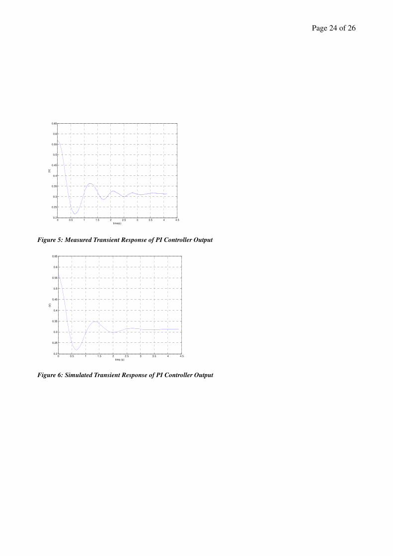
5 Test Results
To verify the proposed design of the DC offset controller, the predictions of equations 10, 11 and 13
were compared with test results. Using the chosen value for τf of 0.1s and the estimated value of
0.07 for k, equation 13 predicts marginal stability of the DC offset control loop when τi is equal to
23ms . With all controller parameters held constant and τi varied, the measured value of τi at the
onset of instability was found to be 20ms. A design value of 100ms was chosen to avoid instability.
A higher value would improve stability but would result in sluggish responses.
Figure 5 shows a measured transient response. The inverter was first left to run with the DC offset
controller not operating. This was done by grounding the output to the DC offset controller. The
controller was then activated by removing the short. The transient response of the integrator
capacitor consists of the voltage changing from its initial value to the steady-state value required for
elimination of any DC offset. Prediction of the controller response, which was carried out using
equations (10) and (11), is shown in figure 6. There is in reasonable agreement between the
predicted response and the measured response shown in figure 5. Transients such as the one shown
in figure 6 are easily avoided if a digital version of the DC offset controller is used.
Figures 7 and 8 and table 2 provide additional experimental results. Figure 7 is a comparison of the
DC offset sensor output waveform (vo) with and without the DC offset controller in operation. The
50 Hz component in vo is quite prominent compared to the DC content. Figure 8 illustrates the
absence of interaction between the DC bus voltage control loop and the DC offset control loop. The

Page 15 of 26
DC offset control loop is opened by forcing the controller output to zero at time t1. The loop is
closed again at time t2. As shown in figure 8, the DC offset current signal, which has been extracted
from the output of the DC offset sensor by additional filtering, responds accordingly. It increases as
a result of the DC offset loop being opened and returns to zero after a transient period upon closure
of the loop. Clearly, the DC bus voltage, also shown in figure 8, is unaffected by operation of the
DC offset control loop.
It was found that without a DC offset control loop the level of DC offset current was a function of
inverter output. As shown in table 2, the DC offset controller operates to ensure that the DC offset
current remains within acceptable limits irrespective of the level of inverter output current.
6. Conclusions
A simple feedback system has been proposed to practically eliminate any DC offset from the output
of a single phase transformerless grid-connected inverter. It is demonstrated that design of the
feedback system is greatly simplified since, from a control point of view, the DC offset control loop
is decoupled from other feedback loops controlling the inverter.
DC offset is monitored by sensing the voltage across the ripple filter inductor. The DC signal is
extracted by using simple two-stage RC filtering. An analogue PI controller is used which ideally
results in zero steady state error. In practice a small DC offset remains, but this is well within the
limits imposed by standards such as Australian Standard AS4777.2 or the United Kingdom’s ER
G83/1.
The analogue PI controller performs very satisfactorily and its component count and cost are very
low. However, digital implementation of the controller has advantages such as ease of adjustment
of controller parameters and better control of integrator initial conditions at inverter start-up.

Page 16 of 26
References
[1] K. Masoud and G. Ledwich, “Grid Connection Without Mains Transformers,” Journal of
Electrical and Electronic Engineering, vol.19 (1/2), pp31-36, 1999.
[2] A. Ahfock and A. Hewitt , “DC Magnetisation of Transformers,” IEE Proc. in Electrical
Power Applications, vol. 153, (4),pp601-607,2006.
[3] S. Bradley and J. Crabtree, Effects of DC from Embedded Generation on Residual Current
Devices and Single-Phase Metering, EA Technology, report No. WS4-P11, 2005.
[4] V. Salas, E. Olias. M. Alonso and F. Chenlo, Overview of the legislation of DC injection in
the network for low voltage small grid-connected PV systems in Spain and other countries,
Renewable and Sustainable Reviews, vol 12, Issue 2, February 2008, pp575-583.
[5] AS 4777.2, Grid Connection of Energy Systems via Inverters Part 2: Inverter Requirements,
Australia, 2002.
[6] ER G83/1, Recommendations for the Connection of Small-Scale Embedded Generators (up
to 16 A per phase) in parallel with public low-voltage distribution networks, United
Kingdom, September 2003.
[7] H. Haeberlin, Ch. Liebi, and Ch. Beutler, Inverters for Grid-Connected PV Systems: Test
Results of Some New Inveters and Latest Reliabilty Data of Most Popular Inverters in
Switzerland, 14th
European Photovoltaic Solar Energy Conference Barcelona (Catalunya)
Spain, June/July 1997.

Page 17 of 26
[8] V. Salas, E. Olias, M. Alonso, F. Chenlo and A. Barrado, DC Current Injection into the
Network from PV Grid Inverters, IEEE 4th
World Conference on Photovoltaic Energy
Conversion, May 2006, pp2371-2374.
[9] R Sharma, Removal of DC Offset Current from Transformerless PV Inverters Connected to
Utility, Proceedings of the 40th
International Universities Power Engineering Conference,
Cork Institute of Technology, Ireland, pp1230-1234, 2005.
[10] M.Armstrong, D.J.Atkinson, C.Mark Johnson, Auto-Calibrating DC Link Current Sensing
Technique for Transformerless, Grid Connected, H-Bridge Inverter Systems, IEEE
Transactions on Power Electronics, September 2006, volume 21, No 5, pp1385-1393.
[11] A. Ahfock and L. Bowtell, DC Offset Elimination in a Transformerless Single Phase Grid-
Connected Photovoltaic System, Australasian Universities Power Engineering Conference,
AUPEC 06, Victoria University, Melbourne, September 2006.
[12] M.Calais J.Myrzik, T.Spooner and V.G.Agelidis, Inverters for Single-Phase Grid Connected
Phototvoltaic Systems – an Overview, IEEE 33rd
annual Power Electronics Specialists
Conference, vol 4, pp 1995-2000, 2002
[13] C.M.Liaw, T.H.Chen, T.C.Wang, G.J.Cho, C.M.Lee and C.T.Wang, Design and
Implementation of a single phase current-forced switching mode bilateral convertor, IEE
Proceedings-B, vol 138, No. 3, pp129-136, May 1991.
[14] G.M.S. Azevedo, M.C.Cavalcanti, K.C.Oliveira, F.A.S.Neves and Z.D.Lins, Comparative
Evaluation of Maximum Power Point Tracking Methods for Photovoltaic Systems, American
Society of Mechanical Engineering, Journal of Solar Energy, Engineering, vol. 131, pp
031006-1/8, 2009 .

Page 18 of 26
Table 1 : DC Offset Controller Design Parameters
Design variable Chosen value Comments
Current
Sensor
constant
(kh)
1.25 V/A
• Determined by number of turns used with the Hall-
Effect sensor.
• Inadequate sensitivity if value too low
• Maximum value limited by DC rail voltage
AC component
in DC offset
controller
output signal
(khic)
10mV
• Represents the undesirable 50Hz component in the
output of the DC offset sensor.
• Chosen limit dictates the value of the filter time
constant τf given by equation 9.
• If chosen limit is too small, τf becomes too large
making the filter harder to implement
Filter resistance(Rf)
and
Filter capacitance(C)
220kΩΩΩΩ
0.47uF
• Rf C or τf is dictated by equation 9
• Rf cannot be made larger than a few hundred kΩ
because of the effect of noise and stray impedances
Series resistance (R)
0.2ΩΩΩΩ
• Can consist of just the inductors’ resistance or
additional series resistance may be added.
• Choice of R dictated by efficiency considerations.
PI controller
gain (kp)
0.4
• For a given degree of stability, increasing kp will
mean increasing τi, making integrator
implementation difficult
• Too low a value of kp leads to sluggish controller
response.
PI controller
Integration
time (τ i )
100ms
• For the chosen value of k, defined as kpR / kh ,
inequality 13 predicts a τi value of 23ms for
marginal stability
• A value of τi sufficiently higher than 23ms was
chosen to ensure adequate damping.

Page 19 of 26
Table 2 : DC Offset Currents
Inverter AC Output
Current
(A rms)
Inverter DC offset current(mA)
with control loop open
Inverter DC offset current (mA)
with control loop closed
1.0 A 30mA 1.02mA
2.0A
13mA
0.86mA
3.0A
-8.1mA
0.52mA
4.0A
-22mA
0.61mA

Page 20 of 26
i
ip
svcv
s
Figure 1: Grid-Connected PV System

Page 21 of 26
DB+
DB-
Voltage Controller
(PI)
Hysteretic Current
Controller
and
Gate Drive Module
vsks
vce
ikh
vref
vckc
kc
irefkhipkd
Maximum
Power
Tracker
From
Solar
Panels
T
TA+ TB+
B -
DA -
D D
DB-
sv
ip
cv
TA -
A+
A Bi
Hall Effect
Current Sensor
(from differential
amplifier)
ov
Gate
Signals
L L
fv
kc, kd,kh and ks are current or voltage sensor constants
isr
1v
N
C
C
Rf
Rf
Cr
Figure 2: Inverter Main Components and DC Offset Sensor

Page 22 of 26
Figure 3: Inverter Output Current Waveform ( Iref = 3A)

Page 23 of 26
Figure 4: DC offset sensor block diagram
Page 24 of 26
0 0.5 1 1.5 2 2.5 3 3.5 4 4.50.2
0.25
0.3
0.35
0.4
0.45
0.5
0.55
0.6
0.65
time(s)
(V)
Figure 5: Measured Transient Response of PI Controller Output
0 0.5 1 1.5 2 2.5 3 3.5 4 4.50.2
0.25
0.3
0.35
0.4
0.45
0.5
0.55
0.6
0.65
time (s)
(V)
Figure 6: Simulated Transient Response of PI Controller Output

Page 25 of 26
Figure7: DC Offset sensor output

Page 26 of 26
Figure 8: Interaction between the DC offset controller and the DC bus voltage controller