Embed Size (px)
Citation preview
A Custom Serial Peripheral Interface (SPI) BusSlave Controller with Read/Write Register Banks
Vladimir Milovanovic, Senior Member, IEEE, and Darko Tasovac, Member, IEEE
Abstract—Interchip communications often exploit the so-calledserial peripheral interface (SPI) bus for lower-level and medium-speed exchange of data. Typical use cases include application-specific integrated circuit (ASIC) setup and testing via scanchain. A lack of formal standardization and ubiquitous presenceinevitably lead to abundance of SPI protocol definitions. Thispaper presents a custom SPI bus slave controller which includessingle and block addressable bank of read-only status, as wellas read/write configuration registers. The controller employs arather efficient in-frame addressing scheme which is supportedby low-propagation register bank design. Thanks to these two, theFPGA bus implementation managed to be clocked at 100 MHz,thus effectively achieving a 100 Mbit/s burst data throughput.
Index Terms—SPI, serial peripheral interface bus, serial link,serial communication, master and slave controller, register bank.
I. INTRODUCTION
SERIAL communication can be described as the process ofsequentially sending single bit data at a time, over a bus
or communication channel in general. In telecommunication,this contrasts the parallel communication, in which several bitsare sent as a whole, on a link with several parallel channels.
Serial type of communication is used for literally everylong-haul communication and most computer networks, wherethe cost of cable and synchronization difficulties make parallelcommunication impractical. The advantages of parallel datatransmission (i.e., no need for SerDes or serializer and dese-rializer) are outweighed by an improved signal integrity andtransmission speeds in newer serial technologies [1] makingserial computer buses more common even at shorter distances.
Although serial links might, at first, seem inferior to parallelones, since they can transmit less data per single clock cycle,it is often the case that serial links can be clocked considerablyfaster thus achieving higher data rates. Factors like clock skewand crosstalk between lines, which are far more pronouncedin parallel links, disallow those to be clocked at a higher rates.
Furthermore, in many cases, serial links are simply cheaperto implement than parallel. The vast majority of integratedcircuits (ICs) have serial interfaces [2], as opposed to parallelones, so that they can have fewer pads/pins and hence shrinkdie area and reduce package size and cost. This is always donewhen data transfer speeds are not of paramount importance.
Some examples of such low-cost serial buses for integratedcircuits include SPI, I2C, SMBus, UNI/O, 1-Wire, etc. Gen-erally speaking, many of these communication systems wereoriginally designed to connect two or more integrated circuits.
V. M. Milovanovic is with the Faculty of Engineering, University of Kragu-jevac, Sestre Janjic 6, 34000 Kragujevac, Serbia (e-mail: [email protected]).
Darko Tasovac is with NovelIC Microsystems, Veljka Dugosevica 54/A3,11060 Belgrade, Republic of Serbia (e-mail: [email protected]).
The Serial Peripheral Interface bus (SPI), developed by [2]Motorola in the late seventies, is a synchronous serial commu-nication interface specification used for short distance commu-nication, primarily in connection with integrated circuits andembedded systems. Since then, the interface has become a defacto standard with typical applications which include, but arenot limited to, communication with all sorts of sensors, dataconverters, (flash) memories, real-time clocks (RTCs), varioustypes of displays such as LCDs, and custom integrated circuits.
SPI devices communicate between each other in full duplexmode using a master-slave configuration with a single masterand one or more slaves. Multiple slave devices are supportedthrough selection with individual slave select (SS) lines but themaster device originates the frame for reading and writing.
Sometimes SPI is called a four-wire serial bus, contrastingwith three-wire, two-wire, and one-wire serial buses. Althoughthe SPI is accurately described as a synchronous serial in-terface, it should nevertheless be distinguished from the so-called Synchronous Serial Interface (SSI) protocol, which is acompletely different variant of a four-wire synchronous serialcommunication protocol that employs differential signaling.Even though there are some similarities between the SPI busand the JTAG protocol, they are not interchangeable. The SPIbus is intended for much higher speeds, on board initializationof device peripherals, while the JTAG protocol is utilized toprovide reliable test access to the I/O pins from an off boardcontroller with less precise signal delay and skew parameters.
Advantages of the SPI over the competing serial commu-nication protocols are mostly connected to higher achievablethroughput. It is usually categorized [1] as relatively short-distance and medium-speed interface (clock is not limited toany maximum speed). Moreover, since the default version ofthe SPI protocol defines all signals as unidirectional, bothGalvanic isolation and software implementation are feasible.
Among the main disadvantages of the SPI bus are absence ofmultiple master device support, no formal standard definition,and finally, a lack of hardware slave acknowledgment allowingthe master to transmit basically nowhere and not knowing it.
SPIMaster
SCLKMOSIMISO
SS
SCLKMOSIMISOSS
SPISlave
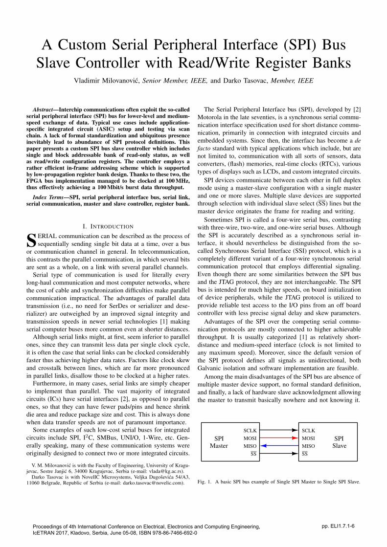
Fig. 1. A basic SPI bus example of Single SPI Master to Single SPI Slave.
Proceedings of 4th International Conference on Electrical, Electronics and Computing Engineering, IcETRAN 2017, Kladovo, Serbia, June 05-08, ISBN 978-86-7466-692-0
pp. ELI1.7.1-6
II. THE SERIAL PERIPHERAL INTERFACE (SPI) BUS
The standard four-wire Serial Peripheral Interface (SPI) bus,as depicted in Fig. 1, specifies the following four logic signals:
• SCLK or SCK: Serial Clock (generated by the master);• MOSI: Master Output Slave Input (data out from master);• MISO: Master Input Slave Output (data out from slave);• SS: Slave Select (often active low, output from master).
The above pin names are currently the most popular. In thepast, alternative pin naming conventions were sometimes used,and so the SPI port pin names for older IC products may differ.Slave Select (SS) fundamentally has the same functionality asChip Select (CS) and is used instead of an addressing concept.If a single slave device is used, the SS pin may be fixed tologic low if the slave permits it. However, some slaves requirea falling edge of the chip select signal to initiate an action.
All slave devices intended for operation in multi-slave SPIenvironments posses tri-state outputs so that their MISO signalbecomes high impedance (logically disconnected) when thedevice is not selected. Devices without tri-state outputs cannotshare SPI bus segments with other slaves devices, instead asin Fig. 1, only one such slave device could talk to the master.
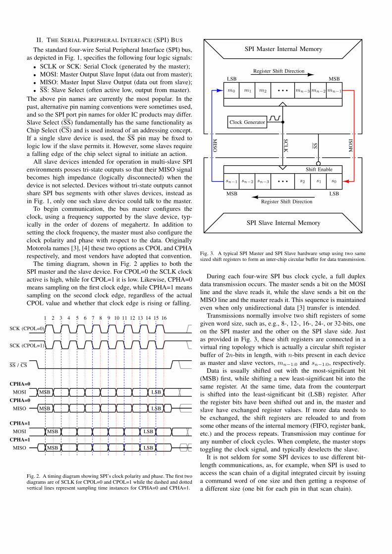
To begin communication, the bus master configures theclock, using a frequency supported by the slave device, typ-ically in the order of dozens of megahertz. In addition tosetting the clock frequency, the master must also configure theclock polarity and phase with respect to the data. OriginallyMotorola names [3], [4] these two options as CPOL and CPHArespectively, and most vendors have adopted that convention.
The timing diagram, shown in Fig. 2 applies to both theSPI master and the slave device. For CPOL=0 the SCLK clockactive is high, while for CPOL=1 it is low. Likewise, CPHA=0means sampling on the first clock edge, while CPHA=1 meanssampling on the second clock edge, regardless of the actualCPOL value and whether that clock edge is rising or falling.
1 2 3 4 5 6 7 8 9 10 11 12 13 14 15 16
SCK (CPOL=0)
SCK (CPOL=1)
SS / CS
CPHA=0MOSI MSB LSB
CPHA=0MISO MSB LSB
CPHA=1MOSI MSB LSB
CPHA=1MISO MSB LSB
Fig. 2. A timing diagram showing SPI’s clock polarity and phase. The first twodiagrams are of SCLK for CPOL=0 and CPOL=1 while the dashed and dottedvertical lines represent sampling time instances for CPHA=0 and CPHA=1.
SPI Master Internal Memory
Register Shift DirectionLSB MSB
m0 m1 m2 mn−3 mn−2 mn−1
Clock Generator
MISO
SCL
K SS
MO
SI
Shift Enable
sn−1 sn−2 sn−3 s2 s1 s0
MSB LSBRegister Shift Direction
SPI Slave Internal Memory
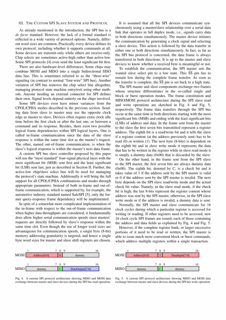
Fig. 3. A typical SPI Master and SPI Slave hardware setup using two samesized shift registers to form an inter-chip circular buffer for data transmission.
During each four-wire SPI bus clock cycle, a full duplexdata transmission occurs. The master sends a bit on the MOSIline and the slave reads it, while the slave sends a bit on theMISO line and the master reads it. This sequence is maintainedeven when only unidirectional data [3] transfer is intended.
Transmissions normally involve two shift registers of somegiven word size, such as, e.g., 8-, 12-, 16-, 24-, or 32-bits, oneon the SPI master and the other on the SPI slave side. Justas provided in Fig. 3, these shift registers are connected in avirtual ring topology which is actually a circular shift registerbuffer of 2n-bits in length, with n-bits present in each deviceas master and slave vectors, mn−1:0 and sn−1:0, respectively.
Data is usually shifted out with the most-significant bit(MSB) first, while shifting a new least-significant bit into thesame register. At the same time, data from the counterpartis shifted into the least-significant bit (LSB) register. Afterthe register bits have been shifted out and in, the master andslave have exchanged register values. If more data needs tobe exchanged, the shift registers are reloaded to and fromsome other means of the internal memory (FIFO, register bank,etc.) and the process repeats. Transmission may continue forany number of clock cycles. When complete, the master stopstoggling the clock signal, and typically deselects the slave.
It is not seldom for some SPI devices to use different bit-length communications, as, for example, when SPI is used toaccess the scan chain of a digital integrated circuit by issuinga command word of one size and then getting a response ofa different size (one bit for each pin in that scan chain).
III. THE CUSTOM SPI SLAVE SYSTEM AND PROTOCOL
As already mentioned in the introduction, the SPI bus is ade facto standard. However, the lack of a formal standard isreflected in a wide variety of protocol options. Namely, differ-ent word sizes are common. Practically every device defines itsown protocol, including whether it supports commands at all.Some devices are transmit-only while others are receive-only.Chip selects are sometimes active-high rather than active-low.Some SPI protocols [4] even send the least significant bit first.
There are also hardware-level differences. Some chips maycombine MOSI and MISO into a single bidirectional SISOdata line. This is sometimes referred to as the “three-wire”signaling (in contrast to normal “four-wire” SPI bus). Anothervariation of SPI bus removes the chip select line altogether,managing protocol state machine entry/exit using other meth-ods. Anyone needing an external connector for SPI definestheir own. Signal levels depend entirely on the chips involved.
Some SPI devices even have minor variances from theCPOL/CPHA modes described in the previous section. Send-ing data from slave to master may use the opposite clockedge as master to slave. Devices often require extra clock idletime before the first clock or after the last one, or between acommand and its response. Besides, there exist two possiblelogical frame dependencies within SPI logical layers. One iscalled in-frame communication since the data of the slaveresponse is within the same time slot as the master’s request.The other, named out-of-frame communication, is when theslave’s logical response is within the master’s next data frame.
A custom SPI bus slave controller proposed by this paperwill use the “most standard” four-signal physical layer with themost significant bit (MSB) sent first and the least significantbit (LSB) sent last, just as described in Section II. Further, theactive-low chip/slave select line will be used for managingthe protocol’s state machine. Additionally it will bring the fullsupport for all CPOL/CPHA combinations and modes throughappropriate parameters. Instead of both in-frame and out-of-frame communication, which is supported by, for example, theautomotive industry standard named SafeSPI [5], only the for-mer query-response frame dependency will be implemented.
In spite of a somewhat more complicated implementation ofthe in-frame with respect to the out-of-frame communicationwhen higher data throughputs are considered, it fundamentallydoes allow higher serial communication speeds since masters’requests are directly followed by slave’s response within thesame time slot. Even though the use of longer word sizes areadvantageous for communication speeds, a single byte (8-bit)memory addressing granularity is targeted, and hence a singlebyte word sizes for master and slave shift registers are chosen.
1
1
7
7
8
8
9
9
16
16
MOSI
MISO
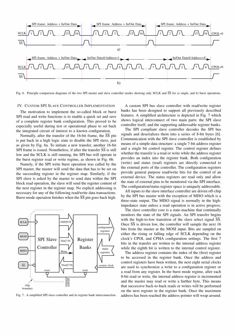
Address[6:0] 0 dummy
dummy C DataOutput[7:0]
Fig. 4. A custom SPI protocol architecture showing MISO and MOSI dataexchange between master and slave devices during the SPI bus read operation.
It is assumed that all the SPI devices communicate syn-chronously using a master/slave relationship over a serial datalink that operates in full duplex mode, i.e., signals carry datain both directions simultaneously. The master device initiatesthe communication by generating a clock signal and selectinga slave device. This action is followed by the data transfer ineither one or both directions simultaneously. In fact, as far asthe SPI bus protocol is concerned, the data frame is alwaystransferred in both directions. It is up to the master and slavedevices to know whether a received byte is meaningful or not.
To establish the communication, the SPI master sets thewanted slave select pin to a low state. This SS pin has toremain low during the complete frame transfer. As soon asthe transfer is complete, the SS pin is set back to a high state.
The SPI master and slave components exchange two frameswhose structure differentiates in the so-called single andblock or burst operation modes. The frame constitution andMISO/MOSI protocol architecture during the SPI slave readand write operations are sketched in Fig. 4 and Fig. 5,respectively. The frame data transfers through the SPI busoccur at the same time in both directions starting with the mostsignificant bits (MSB) and ending with the least significant bits(LSB) of address and data. In the frame sent from the masterto the slave the first seven bits transmitted represent a registeraddress. The eighth bit is a read/write bit and it tells the slaveif a register content (at the address previously sent) has to beread (0) or written (1). The next byte (8-bits) is dependent onthe eighth bit and in slave write mode it represents the datathat has to be written in the register while in slave read mode itis simply a dummy data (0x00) that is discarded by the slave.
On the other hand, in the frame sent from the SPI slaveto the SPI master, the first seven bits are always dummy data(0x00). The eighth bit, denoted by C, is a check bit and ittakes value of 1 if the address sent by the SPI master is validor 0 if the address sent by the SPI master is invalid. The nextbyte depends on the SPI slave read/write mode and the actualcheck bit value. Namely, in the slave read mode, if the checkbit is high, the last 8-bits represent the register content whoseaddress was sent by the SPI master, otherwise, in the SPI slavewrite mode or if the address is invalid, a dummy data is sent.
Normally, the SPI master and slave communicate for 16clock cycles during which a particular register is accessed forwriting or reading. If other registers need to be accessed, new16 clock cycle SPI frames are issued, each of those containingthe address and data fields as explained by Fig. 4 and Fig. 5.
However, if the complete register bank, or larger successiveportions of it need to be read or written, the SPI master isable to issue much more convenient block or burst commands,which address multiple registers within a single transaction.
1
1
7
7
8
8
9
9
16
16
MOSI
MISO
Address[6:0] 1 DataInput[7:0]
dummy C dummy
Fig. 5. A custom SPI protocol architecture showing MISO and MOSI dataexchange between master and slave devices during the SPI bus write operation.
SPI frame: Address + In/Out Data SPI frame: Address + In/Out Data SPI frame: Address + In/Out Data
SCLK 1 1 12 2 23 3 315 15 1516 16 16 CPOL=0
SS
a)
SPI frame: Address + In/Out Data In/Out Data@Address+1 In/Out Data@Address+K
SCLK 1 2 3 15 16 1 1 12 2 27 7 78 8 8 CPOL=0
SS
b)
Fig. 6. Principle comparison diagrams of the two SPI master and slave controller modes showing only SCLK and SS for a) single, and b) burst operations.
IV. CUSTOM SPI SLAVE CONTROLLER IMPLEMENTATION
The motivation to implement the so-called block or burstSPI read and write functions is to enable a quick set and saveof a complete register bank configuration. This proved to beespecially useful during test or operational phase to set backthe integrated circuit of interest to a known configuration.
Normally, after the transfer of the 16-bit frame, the SS pinis put back in a high logic state to disable the SPI slave, justas given by Fig. 6a. To initiate a new transfer, another 16-bitSPI frame is issued. Nonetheless, if after the transfer SS is stilllow and the SCLK is still running, the SPI bus will operate inthe burst register read or write regime, as shown in Fig. 6b.
Namely, if the SPI write burst operation was called by theSPI master, the master will send the data that has to be set onthe succeeding register in the register map. Similarly, if theSPI slave is asked by the master to send data within the SPIblock read operation, the slave will send the register content ofthe next register in the register map. No explicit addressing isnecessary for any of the following read/write data transactions.Burst-mode operation finishes when the SS pin goes back high.
SPI Slave
Controller
Register
Banks
SCLK
MOSI
MISO
SS
Addr[6:0]
Din[7:0]
Write
Dout[7:0]
configurationregisters
statusregisters
system clock
reset reset
RE
SET��
chipboundary
Fig. 7. A simplified SPI slave controller and its register bank interconnection.
A custom SPI bus slave controller with read/write registerbanks has been designed to support all previously describedfeatures. A simplified architecture is depicted in Fig. 7 whichshows logical interconnect of two main parts: the SPI slavecontroller itself, and the supporting addressable register banks.
The SPI compliant slave controller decodes the SPI bussignals and deserializes them into a series of 8-bit bytes [6].Communication with the SPI slave controller is established bymeans of a simple data structure: a single 7-bit address registerand a single bit control register. The control register defineswhether the transfer is a read or write while the address registerprovides an index into the register bank. Both configuration(write) and status (read) registers are directly connected tothe external ports of the controller. The configuration registersprovide general purpose read/write bits for the control of anexternal device. The status registers are read only and allowthe state of external pins to be monitored via the SPI interface.The configuration/status register space is uniquely addressable.
All inputs to the slave interface controller are driven off-chipby the SPI bus master with the exception of MISO which is athree-state output. The MISO signal is normally in the high-impedance state unless a read operation is in active progress.
The slave controller core is a state-machine that continuallymonitors the state of the SPI signals. An SPI transfer beginswith the high-to-low transition of the slave select signal SS.Once SS is driven low, the controller will sample the next 16bits from the master at the MOSI input. Bits are sampled oneither the rising or falling edge of SCLK depending on theclock’s CPOL and CPHA configuration settings. The first 7bits in the transfer are written to the internal address registerwhile the eighth bit is written to the internal control register.
The address register contains the index of the (first) registerto be accessed in the register bank. Once the address andcontrol registers have been written, the next eight serial clocksare used to synchronize a write to a configuration register ora read from any register. In the burst mode regime, after each8-bit read or write, the internal address register is incrementedand the master may read or write a further byte. This meansthat successive back-to-back reads or writes will be performedon the next register in the register bank. Once the maximumaddress has been reached the address pointer will wrap around.
DataInput[7:0]
Write synchronizer WriteEnable(WE) WE
REG 2N-1WE
REG 2N-2WE
REG 2N-3WE
REG 2N-4
WEREG 7
WEREG 6
WEREG 5
WEREG 4
WEREG 3
WEREG 2
WEREG 1
WEREG 0
dem
uxde
mux
dem
ux
BANK#2N-2-1
BA
NK
#1
BANK#0
2N-2-1
N-2
–to–2
N-2
Dec
oder
3210
Addr[N-1]
Addr[3]Addr[2]
Addr[1]Addr[0]
systemclock
domain
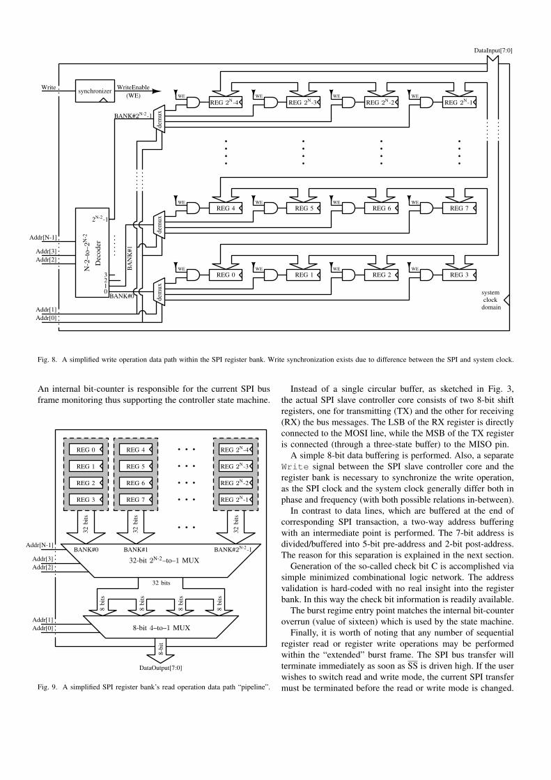
Fig. 8. A simplified write operation data path within the SPI register bank. Write synchronization exists due to difference between the SPI and system clock.
An internal bit-counter is responsible for the current SPI busframe monitoring thus supporting the controller state machine.
Addr[N-1]
Addr[3]Addr[2]
Addr[1]Addr[0]
REG 0
REG 1
REG 2
REG 3
REG 4
REG 5
REG 6
REG 7
REG 2N-4
REG 2N-3
REG 2N-2
REG 2N-1
32bi
ts
32bi
ts
32bi
ts
BANK#0 BANK#1 BANK#2N-2-1
32-bit 2N-2–to–1 MUX
32 bits
8bi
ts
8bi
ts
8bi
ts
8bi
ts
8-bit 4–to–1 MUX
8-bi
t
DataOutput[7:0]
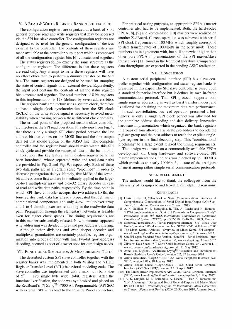
Fig. 9. A simplified SPI register bank’s read operation data path “pipeline”.
Instead of a single circular buffer, as sketched in Fig. 3,the actual SPI slave controller core consists of two 8-bit shiftregisters, one for transmitting (TX) and the other for receiving(RX) the bus messages. The LSB of the RX register is directlyconnected to the MOSI line, while the MSB of the TX registeris connected (through a three-state buffer) to the MISO pin.
A simple 8-bit data buffering is performed. Also, a separateWrite signal between the SPI slave controller core and theregister bank is necessary to synchronize the write operation,as the SPI clock and the system clock generally differ both inphase and frequency (with both possible relations in-between).
In contrast to data lines, which are buffered at the end ofcorresponding SPI transaction, a two-way address bufferingwith an intermediate point is performed. The 7-bit address isdivided/buffered into 5-bit pre-address and 2-bit post-address.The reason for this separation is explained in the next section.
Generation of the so-called check bit C is accomplished viasimple minimized combinational logic network. The addressvalidation is hard-coded with no real insight into the registerbank. In this way the check bit information is readily available.
The burst regime entry point matches the internal bit-counteroverrun (value of sixteen) which is used by the state machine.
Finally, it is worth of noting that any number of sequentialregister read or register write operations may be performedwithin the “extended” burst frame. The SPI bus transfer willterminate immediately as soon as SS is driven high. If the userwishes to switch read and write mode, the current SPI transfermust be terminated before the read or write mode is changed.
V. A READ & WRITE REGISTER BANK ARCHITECTURE
The configuration registers are organized as a bank of 8-bitgeneral purpose read and write registers that may be accessedvia the SPI bus slave controller. The configuration registers aredesigned to be used for the general configuration of devicesexternal to the controller. The contents of these registers aremade available at the controller output port which is composedof all the configuration register bits [6] concatenated together.
The status registers follow exactly the same structure as theconfiguration registers. The difference is that these registersare read only. Any attempt to write these registers will haveno effect other than to perform a dummy transfer on the SPIbus. The status registers are designed to be used for snoopingthe state of control signals in an external device. Equivalently,the input port contains the contents of all the status registerbits concatenated together. The total number of 8-bit registersin this implementation is 128 (defined by seven address bits).
The register bank architecture uses a system clock, thereforeat least a single clock synchronization from the SPI clock(SCLK) on the write strobe signal is necessary to avoid meta-stability when crossing between these different clock domains.
The critical point of the proposed custom slave controllerarchitecture is the SPI read operation. It is obvious from Fig. 4,that there is only a single SPI clock period between the lastaddress bit that comes on the MOSI line and the first outputdata bit that should appear on the MISO line. The completecontroller and the register bank should react within this SPIclock cycle and provide the requested data to the bus output.
To support this key feature, an innovative register bank hasbeen introduced, whose separated write and read data pathsare provided in Fig. 8 and Fig. 9, respectively. Both of thesetwo data paths are in a certain sense “pipelined” in order todecrease propagation delays. Namely, five MSBs of the seven-bit address come first and are immediately applied to the larger32-to-1 multiplexer array and 5-to-32 binary decoder in caseof read and write data paths, respectively. By the time point inwhich SPI slave controller accepts the two address LSBs, thefour-register bank data has already propagated through majorcombinational components and only 4-to-1 multiplexer arrayand 1-to-4 demultiplexer are remaining in the read/write datapath. Propagation through the elementary networks is feasibleeven for higher clock speeds. The timing requirements arein this manner substantially relaxed. Now it becomes apparentwhy addressing was divided in pre- and post-address buffering.
Although other divisions and even deeper decoder andmultiplexer granularities are certainly possible, register orga-nization into groups of four with final two-bit (post-address)decoding, seemed as sort of a sweet spot for our design needs.
VI. FUNCTIONAL SIMULATION & MEASUREMENT TESTS
The described custom SPI slave controller together with theregister banks was implemented in both Verilog and VHDLRegister-Transfer Level (RTL) behavioral modeling code. Theslave controller was implemented with a maximum bank sizeof 27 = 128 single byte wide (8-bit) registers. After thefunctional verification, the code was synthesized and placed onthe ZedBoard’s [7] ZynqTM-7000 All Programmable (AP) SoCwith external SPI wires lead to the PL-side Pmod connectors.
For practical testing purposes, an appropriate SPI bus mastercontroller also had to be implemented. Both, the hard-codedFPGA [8], [9] and kernel-based [10] masters were realized onanother ZedBoard. Correct operation was achieved with serialSPI clock frequencies of 100 MHz which roughly correspondto data transfer rates of 100 Mbit/s in the burst mode. Thesenumbers are in agreement with, but still somewhat higher thanother pure FPGA implementations of the SPI master/slavetransceivers [11] found in the technical literature. Comparabledata throughputs are expected in the pending ASIC realization.
VII. CONCLUSION
A custom serial peripheral interface (SPI) bus slave con-troller together with configuration and status register banks ispresented in this paper. The SPI slave controller is based upona standard four-wire interface but it defines its own in-framecommunication protocol. This SPI protocol supports bothsingle register addressing as well as burst transfer modes, andis tailored for obtaining the maximum data rate performance.
In such constellation, bus read operation presented a bot-tleneck as only a single SPI clock period was allocated forthe complete address decoding and data delivery. Innovativehardware implementation which organized the bank registersin groups of four allowed a separate pre-address to decode theregister group and the post-address to reach the explicit single-byte register in the final decoding step. This “combinationalpipelining” to a large extent relaxed the timing requirements.
This design was tested on a commercially available FPGAdevelopment kit. Using hardware- and software-based SPImaster implementations, the bus was clocked up to 100 MHzwhich translates to nearly 100 Mbit/s, a state of the art figureof merit among rather simple serial communication protocols.
ACKNOWLEDGEMENTS
The authors would like to thank the colleagues from theUniversity of Kragujevac and NovelIC on helpful discussions.
REFERENCES
[1] Louis E. Frenzel, “Handbook of Serial Communications Interfaces: AComprehensive Compendium of Serial Digital Input/Output (I/O) Stan-dards”, 1st Edition, Newnes Books – Elsevier, 2015
[2] A. K. Oudjida, M. L. Berrandjia, R. Tiar, A. Liacha and K. Tahraoui,“FPGA Implementation of I2C & SPI Protocols: A Comparative Study”,Proceedings of the 16th IEEE International Conference on Electronics,Circuits and Systems (ICECS), pp. 507-510, 13-16 Dec. 2009, Tunisia
[3] Motorola/Freescale/NXP, “Serial Peripheral Interface (SPI) Block UserGuide”, version 3.06, document number: S12SPIV3/D, 4 February 2003
[4] The Linux Kernel Archives, “Overview of Linux Kernel SPI Support”,www.kernel.org/doc/Documentation/spi/spi-summary, 2 February 2012
[5] SafeSPI Open Standard Specification, “SafeSPI – Serial Peripheral Inter-face for Automotive Safety”, version 1.0, www.safespi.org, 3 June 2016
[6] ZIPcores Data Sheet, “SPI Slave Serial Interface Controller”, version 1.1,www.zipcores.com/datasheets/spi slave.pdf, 31 May 2012
[7] Avnet and Digilent, “ZedBoard (ZynqTMEvaluation and DevelopmentBoard) Hardware User’s Guide”, version 2.2, 27 January 2014
[8] Xilinx Data Sheet, “LogiCORE’s IP AXI Serial Peripheral Interface (AXISPI)”, version 1.02a, 18 January 2012
[9] Xilinx Product Guide, “LogiCORE’s IP AXI Quad Serial PeripheralInterface (AXI Quad SPI)”, version 3.2, 5 April 2017
[10] The Linux Driver Implementers API Guide, “Serial Peripheral Interface(SPI)”, www.kernel.org/doc/html/latest/driver-api/spi.html, 1 May 2017
[11] A. K. Oudjida, M. L. Berrandjia, A. Liacha, R. Tiar, K. Tahraoui andY. N. Alhoumays, “Design and Test of General-Purpose SPI Master/SlaveIPs on OPB bus”, Proceedings of the 7th International Multi-Conferenceon Systems, Signals and Devices (SSD), 27-30 June 2010, Amman, Jordan