Embed Size (px)
Citation preview

REV. 0
Information furnished by Analog Devices is believed to be accurate andreliable. However, no responsibility is assumed by Analog Devices for itsuse, nor for any infringements of patents or other rights of third parties thatmay result from its use. No license is granted by implication or otherwiseunder any patent or patent rights of Analog Devices.
aAD7708/AD7718
One Technology Way, P.O. Box 9106, Norwood, MA 02062-9106, U.S.A.
Tel: 781/329-4700 www.analog.com
Fax: 781/326-8703 © Analog Devices, Inc., 2001
8-/10-Channel, Low Voltage,Low Power, - ADCs
FUNCTIONAL BLOCK DIAGRAM
DVDD XTAL1 XTAL2
MUX
POS BUF
- ADC*
AIN1AIN2AIN3AIN4
PGA
OSCANDPLL
SERIALINTERFACE
ANDCONTROL
LOGIC
DOUTDINSCLKCSRDYRESET
AVDD
I/O PORT
AVDD
AD7708/AD7718
DGND
P2 P1
REFIN2(+)/AIN9 REFIN1(+) REFIN2(–)/AIN10 REFIN1(–)
AINCOM
AIN5AIN6AIN7AIN8
AGND
*AD7708 16-BIT ADC*AD7718 24-BIT ADC
REFIN(+) REFIN(–)
NEG BUF
FEATURES
8-/10-Channel, High Resolution - ADCs
AD7708 Has 16-Bit Resolution
AD7718 Has 24-Bit Resolution
Factory-Calibrated
Single Conversion Cycle Setting
Programmable Gain Front End
Simultaneous 50 Hz and 60 Hz Rejection
VREF Select™ Allows Absolute and Ratiometric
Measurement Capability
Operation Can Be Optimized for
Analog Performance (CHOP = 0) or
Channel Throughput (CHOP = 1)
INTERFACE
3-Wire Serial
SPITM, QSPITM, MICROWIRETM, and DSP-Compatible
Schmitt Trigger on SCLK
POWER
Specified for Single 3 V and 5 V Operation
Normal: 1.28 mA Typ @ 3 V
Power-Down: 30 A (32 kHz Crystal Running)
On-Chip Functions
Rail-to-Rail Input Buffer and PGA
2-Bit Digital I/O Port
APPLICATIONS
Industrial Process Control
Instrumentation
Pressure Transducers
Portable Instrumentation
Smart Transmitters
SPI and QSPI are trademarks of Motorola Inc.MICROWIRE is a trademark of National Semiconductor Corp.VREF Select is a trademark of Analog Devices, Inc.
GENERAL DESCRIPTIONThe AD7708/AD7718 are complete analog front-ends for lowfrequency measurement applications. The AD7718 contains a24-bit Σ-∆ ADC with PGA and can be configured as 4/5 fully-differential input channels or 8/10 pseudo-differential inputchannels. Two pins on the device are configurable as analoginputs or reference inputs. The AD7708 is a 16-bit version ofthe AD7718. Input signal ranges from 20 mV to 2.56 V can bedirectly converted using these ADCs. Signals can be converteddirectly from a transducer without the need for signal conditioning.
The device operates from a 32 kHz crystal with an on-board PLLgenerating the required internal operating frequency. The outputdata rate from the part is software programmable. The peak-to-peak resolution from the part varies with the programmed gainand output data rate.
The part operates from a single 3 V or 5 V supply. When operatingfrom 3 V supplies, the power dissipation for the part is 3.84 mW typ.Both parts are pin-for-pin compatible allowing an upgradablepath from 16 to 24 bits without the need for hardware modifica-tions. The AD7708/AD7718 are housed in 28-lead SOIC andTSSOP packages.

REV. 0–2–
AD7708/AD7718
FEATURES . . . . . . . . . . . . . . . . . . . . . . . . . . . . . . . . . . . . . 1
FUNCTIONAL BLOCK DIAGRAM . . . . . . . . . . . . . . . . . 1
GENERAL DESCRIPTION . . . . . . . . . . . . . . . . . . . . . . . . . 1
AD7718 SPECIFICATIONS . . . . . . . . . . . . . . . . . . . . . . . . 3
AD7708 SPECIFICATIONS . . . . . . . . . . . . . . . . . . . . . . . . 6
TIMING CHARACTERISTICS . . . . . . . . . . . . . . . . . . . . . 9
ABSOLUTE MAXIMUM RATINGS . . . . . . . . . . . . . . . . 10
ORDERING GUIDE . . . . . . . . . . . . . . . . . . . . . . . . . . . . . 10
PIN FUNCTION DESCRIPTIONS . . . . . . . . . . . . . . . . . 12
PIN CONFIGURATION . . . . . . . . . . . . . . . . . . . . . . . . . . 13
ADC CIRCUIT INFORMATION . . . . . . . . . . . . . . . . . . . 15
Signal Chain Overview (CHOP Enabled, CHOP = 0) . . . 15
ADC NOISE PERFORMANCE CHOP ENABLED(CHOP = 0) . . . . . . . . . . . . . . . . . . . . . . . . . . . . . . . . . . . 17
Signal Chain Overview (CHOP Disabled CHOP = 1) . . . 19
ADC NOISE PERFORMANCE CHOP DISABLED(CHOP = 1) . . . . . . . . . . . . . . . . . . . . . . . . . . . . . . . . . . . 20
ON-CHIP REGISTERS . . . . . . . . . . . . . . . . . . . . . . . . . . . 22
Communications Register . . . . . . . . . . . . . . . . . . . . . . . . . . 25
Status Register . . . . . . . . . . . . . . . . . . . . . . . . . . . . . . . . . . . 26
Mode Register . . . . . . . . . . . . . . . . . . . . . . . . . . . . . . . . . . . 27
Operating Characteristics when Addressing theMode and Control Registers . . . . . . . . . . . . . . . . . . . . . . . 28
ADC Control Register . . . . . . . . . . . . . . . . . . . . . . . . . . . . . 28
Filter Register . . . . . . . . . . . . . . . . . . . . . . . . . . . . . . . . . . . 29
I/O Control Register . . . . . . . . . . . . . . . . . . . . . . . . . . . . . . 30
ADC Data Result Register . . . . . . . . . . . . . . . . . . . . . . . . . . 30
Unipolar Mode . . . . . . . . . . . . . . . . . . . . . . . . . . . . . . . . . . 30
Bipolar Mode . . . . . . . . . . . . . . . . . . . . . . . . . . . . . . . . . . . . 31
ADC Offset Calibration Coefficient Registers . . . . . . . . . . . 31
ADC Gain Calibration Coefficient Register . . . . . . . . . . . . . 31
ID Register (ID) . . . . . . . . . . . . . . . . . . . . . . . . . . . . . . . . . 31
User Nonprogrammable Test Registers . . . . . . . . . . . . . . . . 31
Configuring the AD7708/AD7718 . . . . . . . . . . . . . . . . . . . . 32
DIGITAL INTERFACE . . . . . . . . . . . . . . . . . . . . . . . . . . . 34
MICROCOMPUTER/MICROPROCESSORINTERFACING . . . . . . . . . . . . . . . . . . . . . . . . . . . . . . . 34
AD7708/AD7718 to 68HC11 Interface . . . . . . . . . . . . . . . . 34
AD7708/AD7718-to-8051 Interface . . . . . . . . . . . . . . . . . . 35
AD7708/AD7718-to-ADSP-2103/ADSP-2105 Interface . . . 36
BASIC CONFIGURATION . . . . . . . . . . . . . . . . . . . . . . . . 36
Analog Input Channels . . . . . . . . . . . . . . . . . . . . . . . . . . . . 37
Single-Ended Operation . . . . . . . . . . . . . . . . . . . . . . . . . . . 37
Chop Mode of Operation (CHOP = 0) . . . . . . . . . . . . . . . . 37
Nonchop Mode of Operation (CHOP = 1) . . . . . . . . . . . . . 38
Programmable Gain Amplifier . . . . . . . . . . . . . . . . . . . . . . . 38
Bipolar/Unipolar Configuration . . . . . . . . . . . . . . . . . . . . . . 38
Data Output Coding . . . . . . . . . . . . . . . . . . . . . . . . . . . . . . 38
Oscillator Circuit . . . . . . . . . . . . . . . . . . . . . . . . . . . . . . . . . 39
Reference Input . . . . . . . . . . . . . . . . . . . . . . . . . . . . . . . . . . 39
RESET Input . . . . . . . . . . . . . . . . . . . . . . . . . . . . . . . . . . . 39
Power-Down Mode . . . . . . . . . . . . . . . . . . . . . . . . . . . . . . . 39
Calibration . . . . . . . . . . . . . . . . . . . . . . . . . . . . . . . . . . . . . . 40
Grounding and Layout . . . . . . . . . . . . . . . . . . . . . . . . . . . . 40
APPLICATIONS . . . . . . . . . . . . . . . . . . . . . . . . . . . . . . . . 41
Data Acquisition . . . . . . . . . . . . . . . . . . . . . . . . . . . . . . . . . 41
Programmable Logic Controllers . . . . . . . . . . . . . . . . . . . . . 41
Converting Single-Ended Inputs. . . . . . . . . . . . . . . . . . . . . 42
Combined Ratiometric and Absolute ValueMeasurement System . . . . . . . . . . . . . . . . . . . . . . . . . . . . 42
Optimizing Throughput while Maximizing 50 Hzand 60 Hz Rejection in a Multiplexed DataAcquisition System . . . . . . . . . . . . . . . . . . . . . . . . . . . . . . 43
OUTLINE DIMENSIONS . . . . . . . . . . . . . . . . . . . . . . . . . 44
TABLE OF CONTENTS

REV. 0 –3–
AD7708/AD7718
Parameter B Grade Unit Test Conditions
AD7718 (CHOP DISABLED)Output Update Rate 16.06 Hz min CHOP = 1
1.365 kHz maxNo Missing Codes2 24 Bits minResolution 13 Bits p-p ±20 mV Range, SF = 69
18 Bits p-p ±2.56 V Range, SF = 69Output Noise and Update Rates See Tables in
ADC DescriptionIntegral Nonlinearity ±10 ppm of FSR max 2 ppm TypicalOffset Error3 Table VII µV typ Offset Error is in the order of the noise for the
programmed gain and update rate following acalibration
Offset Error Drift vs. Temp4 ±200 nV/°C typFull-Scale Error3 ±10 µV typGain Drift vs. Temp4 ±0.5 ppm/°C typNegative Full-Scale Error ±0.003 % FSR max
ANALOG INPUTSDifferential Input Full-Scale Voltage ±1.024 × REFIN/GAIN V nom REFIN Refers to Both REFIN1 and
REFIN2. REFIN = REFIN(+) –REFIN(–)GAIN = 1 to 128
Absolute AIN Voltage Limits AGND + 100 mV V min AIN1–AIN10 and AINCOM withAVDD – 100 mV V max NEGBUF = 1
Absolute AINCOM Voltage Limits AGND – 30 mV V min NEGBUF = 0AVDD + 30 mV V max
Analog Input Current AIN1–AIN10 and AINCOM with NEGBUF = 1DC Input Current2 ±1 nA maxDC Bias Current Drift ±5 pA/°C typ
AINCOM Input Current NEGBUF = 0DC Input Current2 ±125 nA/V typ ±2.56 V RangeDC Bias Current Drift ±2 pA/V/°C typ
Normal-Mode Rejection2
@ 50 Hz 100 dB min 50 Hz ± 1 Hz, SF Word = 82@ 60 Hz 100 dB min 60 Hz ± 1 Hz, SF Word = 68
Common-Mode Rejection@ DC 90 dB min 100 dB typ, Analog Input = 1 V,
Input Range = ± 2.56 V110 dB typ on ± 20 mV Range
@ 50 Hz 100 dB typ 50 Hz ± 1 Hz, SF Word = 82@ 60 Hz 100 dB typ 60 Hz ± 1 Hz, SF Word = 68
REFERENCE INPUTS (REFIN1 AND REFIN2)REFIN(+) to REFIN(–) Voltage 2.5 V nom REFIN Refers to Both REFIN1 and REFIN2REFIN(+) to REFIN(–) Range2 1 V min
AVDD V maxREFIN Common-Mode Range AGND – 30 mV V min
AVDD + 30 mV V maxReference DC Input Current 0.5 µA/V typReference DC Input Current Drift ±0.1 nA/V/°C typNormal-Mode Rejection2
@ 50 Hz 100 dB min 50 Hz ± 1 Hz, SF Word = 82@ 60 Hz 100 dB min 60 Hz ± 1 Hz, SF Word = 68
Common-Mode Rejection Input Range = ± 2.56 V@ DC 100 dB typ Analog Input = 1 V. Input Range = ± 2.56 V@ 50 Hz 100 dB typ@ 60 Hz 100 dB typ
AD7718 SPECIFICATIONS1(AVDD = 2.7 V to 3.6 V or 4.75 V to 5.25 V, DVDD = 2.7 V to 3.6 V or 4.75 V to 5.25 V,
REFIN(+) = 2.5 V; REFIN(–) = AGND; AGND = DGND = 0 V; XTAL1/XTAL2 = 32.768 kHz Crystal Input Buffer Enabled. All specifications TMIN toTMAX unless otherwise noted.)

REV. 0–4–
AD7718–SPECIFICATIONS1(AVDD = 2.7 V to 3.6 V or 4.75 V to 5.25 V, DVDD = 2.7 V to 3.6 V or 4.75 V to 5.25 V, REFIN(+) =
2.5 V ; REFIN(–) = AGND; AGND = DGND = 0 V; XTAL1/XTAL2 = 32.768 kHz Crystal Input Buffer Enabled. All specifications TMIN to TMAX unless otherwise noted.)
Parameter B Grade Unit Test Conditions
AD7718 (CHOP ENABLED)Output Update Rate 5.4 Hz min CHOP = 0
105 Hz maxNo Missing Codes2 24 Bits min 20 Hz Update RateResolution 13 Bits p-p ± 20 mV Range, 20 Hz Update Rate
18 Bits p-p ± 2.56 V Range, 20 Hz Update RateOutput Noise and Update Rates See Tables in
ADC DescriptionIntegral Nonlinearity ± 10 ppm of FSR max 2 ppm TypicalOffset Error3 ± 3 µV typOffset Error Drift vs. Temp4 10 nV/°C typFull-Scale Error3 ± 10 µV/°C typGain Drift vs. Temp4 ± 0.5 ppm/°C typ
ANALOG INPUTSDifferential Input Full-Scale Voltage ±1.024 × REFIN/GAIN V nom REFIN Refers to Both REFIN1 and
REFIN2. REFIN = REFIN(+) REFIN(–)GAIN = 1 to 128
Range Matching ± 2 µV typ Analog Input = 18 mVAbsolute AIN Voltage Limits AGND + 100 mV V min AIN1–AIN10 and AINCOM with
AVDD – 100 mV V max NEGBUF = 1Absolute AINCOM Voltage Limits AGND – 30 mV V min NEGBUF = 0
AVDD + 30 mV V maxAnalog Input Current AIN1–AIN10 and AINCOM with
NEGBUF = 1DC Input Current2 ± 1 nA maxDC Input Current Drift ± 5 pA/°C typ
AINCOM Input Current NEGBUF = 0DC Input Current2 ± 125 nA/V typ ± 2.56 V RangeDC Bias Current Drift ± 2 pA/V/°C typ
Normal-Mode Rejection2
@ 50 Hz 100 dB min 50 Hz ± 1 Hz, SF Word = 82@ 60 Hz 100 dB min 60 Hz ± 1 Hz, SF Word = 68
Common-Mode Rejection@ DC 90 dB min 100 dB typ, Analog Input = 1 V,
Input Range = ±2.56 V110 dB typ on ± 20 mV Range
@ 50 Hz2 100 dB min 50 Hz ± 1 Hz, 20 Hz Update Rate@ 60 Hz2 100 dB min 60 Hz ± 1 Hz, 20 Hz Update Rate
REFERENCE INPUTS (REFIN1 AND REFIN2)REFIN(+) to REFIN(–) Voltage 2.5 V nom REFIN Refers to Both REFIN1 and
REFIN2REFIN(+) to REFIN(–) Range2 1 V min
AVDD V maxREFIN Common-Mode Range AGND – 30 mV V min
AVDD + 30 mV V maxReference DC Input Current2 ± 0.5 µA/V typReference DC Input Current Drift ± 0.01 nA/V/°C typNormal-Mode Rejection2
@ 50 Hz 100 dB min 50 Hz ± 1 Hz, SF Word = 82@ 60 Hz 100 dB min 60 Hz ± 1 Hz, SF Word = 68
Common-Mode Rejection2 Input Range = ± 2.56 V@ DC 110 dB typ Analog Input = 1 V@ 50 Hz 110 dB typ 50 Hz ± 1 Hz, 20 Hz Update Rate@ 60 Hz 110 dB typ 60 Hz ± 1 Hz, 20 Hz Update Rate
LOGIC INPUTS5
All Inputs Except SCLK and XTAL12
VINL, Input Low Voltage 0.8 V max DVDD = 5 VVINL, Input Low Voltage 0.4 V max DVDD = 3 VVINH, Input High Voltage 2.0 V min DVDD = 3 V or 5 V

REV. 0 –5–
AD7708/AD7718Parameter B Grade Unit Test Conditions
LOGIC INPUTS (Continued)SCLK Only (Schmitt-Triggered Input)2
VT(+) 1.4/2 V min/V max DVDD = 5 VVT(–) 0.8/1.4 V min/V max DVDD = 5 VVT(+) – VT(–) 0.3/0.85 V min/V max DVDD = 5 VVT(+) 0.95/2 V min/V max DVDD = 3 VVT(–) 0.4/1.1 V min/V max DVDD = 3 VVT(+)–VT(–) 0.3/0.85 V min/V max DVDD = 3 V
XTAL1 Only2
VINL, Input Low Voltage 0.8 V max DVDD = 5 VVINH, Input High Voltage 3.5 V min DVDD = 5 VVINL, Input Low Voltage 0.4 V max DVDD = 3 VVINH, Input High Voltage 2.5 V min DVDD = 3 V
Input Currents ± 10 µA max Logic Input = DVDD
–70 µA max Logic Input = DGND, Typical –40 µA @ 5 Vand –20 µA at 3 V
Input Capacitance 10 pF typ All Digital Inputs
LOGIC OUTPUTS (Excluding XTAL2)5
VOH, Output High Voltage2 DVDD – 0.6 V min DVDD = 3 V, ISOURCE = 100 µA
VOL, Output Low Voltage2 0.4 V max DVDD = 3 V, ISINK = 100 µAVOH, Output High Voltage2 4 V min DVDD = 5 V, ISOURCE = 200 µAVOL, Output Low Voltage2 0.4 V max DVDD = 5 V, ISINK = 1.6 mAFloating State Leakage Current ± 10 µA maxFloating State Output Capacitance ± 10 pF typData Output Coding Binary Unipolar Mode
Offset Binary Bipolar Mode
SYSTEM CALIBRATION2
Full-Scale Calibration Limit 1.05 × FS V maxZero-Scale Calibration Limit –1.05 × FS V minInput Span 0.8 × FS V min
2.1 × FS V max
START-UP TIMEFrom Power-On 300 ms typFrom Power-Down Mode 1 ms typ Oscillator Enabled
300 ms typ Oscillator Powered Down
POWER REQUIREMENTSPower Supply Voltages AVDD and DVDD can be operated independently of each other.
AVDD–AGND 2.7/3.6 V min/max AVDD = 3 V nom4.75/5.25 V min/max AVDD = 5 V nom
DVDD–DGND 2.7/3.6 V min/max DVDD = 3 V nom4.75/5.25 V min DVDD = 5 V nom
DIDD (Normal Mode) 0.55 mA max DVDD = 3 V, 0.43 mA typ0.65 mA max DVDD = 5 V, 0.5 mA typ
AIDD (Normal Mode) 1.1 mA max AVDD = 3 V or 5 V, 0.85 mA typDIDD (Power-Down Mode) 10 µA max DVDD = 3 V, 32.768 kHz Osc. Running
2 µA max DVDD = 3 V, Oscillator Powered Down30 µA max DVDD = 5 V, 32.768 kHz Osc. Running8 µA max DVDD = 5 V, Oscillator Powered Down
AIDD (Power-Down Mode) 1 µA max AVDD = 3 V or 5 VPower Supply Rejection (PSR) Input Range = ±2.56 V, AIN = 1 V
Chop Disabled 70 dB min 95 dB typ Chop Enabled 100 dB typ
NOTES1Temperature range is –40°C to +85°C.2Not production tested, guaranteed by design and/or characterization data at release.3Following a self-calibration this error will be in the order of the noise for the programmed gain and update selected. A system calibration will completely remove this error.4Recalibration at any temperature will remove these errors.5I/O Port Logic Levels are with respect to AVDD and AGND.
Specifications are subject to change without notice.

REV. 0–6–
AD7708/AD7718AD7708 SPECIFICATIONS1
(AVDD = 2.7 V to 3.6 V or 4.75 V to 5.25 V, DVDD = 2.7 V to 3.6 V or 4.75 V to 5.25 V,REFIN(+) = 2.5 V; REFIN(–) = AGND; AGND = DGND = 0 V; XTAL1/XTAL2 = 32.768 kHz Crystal Input Buffers Enabled. All specifications TMIN toTMAX unless otherwise noted.)
Parameter B Grade Unit Test Conditions
AD7708 (CHOP DISABLED)Output Update Rate 16.06 Hz min CHOP = 1
1.365 kHz maxNo Missing Codes2 16 Bits minResolution 13 Bits p-p ±20 mV Range, SF Word = 69
16 Bits p-p ±2.56 V Range, SF Word = 69Output Noise and Update Rates See Tables in ADC DescriptionIntegral Nonlinearity ±15 ppm of FSR max 2ppm TypicalOffset Error3 ±0.65 LSB typ Following a Self-CalibrationOffset Error Drift vs. Temp4 ±200 nV/°C typFull-Scale Error3 ±0.75 LSB typGain Drift vs. Temp4 ±0.5 ppm/°C typNegative Full-Scale Error ±0.003 % FSR typ
ANALOG INPUTSDifferential Input Full-Scale Voltage ±1.024 × REFIN/GAIN V nom REFIN Refers to Both REFIN1 and
REFIN2. REFIN = REFIN(+) – REFIN(–)GAIN = 1 to 128
Absolute AIN Voltage Limits AGND + 100 mV V min AIN1–AIN10 and AINCOM withAVDD – 100 mV V max NEGBUF = 1
Absolute AINCOM Voltage Limits AGND – 30 mV V min NEGBUF = 0AVDD + 30 mV V max
Analog Input Current AIN1–AIN10 and AINCOM withNEGBUF = 1
DC Input Current2 ±1 nA maxDC Bias Current Drift ±5 pA/°C typ
AINCOM Input Current NEGBUF = 0DC Input Current2 ±125 nA/V typ ±2.56 V RangeDC Bias Current Drift ±2 pA/V/°C typ
Normal-Mode Rejection2
@ 50 Hz 100 dB min 50 Hz ± 1 Hz, SF Word = 82@ 60 Hz 100 dB min 60 Hz ± 1 Hz, SF Word = 68
Common-Mode Rejection@ DC 90 dB min 100 dB typ, Analog Input = 1 V,
Input Range = ±2.56 V110 dB typ on ± 20 mV Range
@ 50 Hz 100 dB typ 50 Hz ± 1 Hz, SF Word = 82@ 60 Hz 100 dB typ 60 Hz ± 1 Hz, SF Word = 68
REFERENCE INPUTS (REFIN1 AND REFIN2)REFIN(+) to REFIN(–) Voltage 2.5 V nom REFIN Refers to Both REFIN1 and
REFIN2REFIN(+) to REFIN(–) Range2 1 V min
AVDD V maxREFIN Common-Mode Range AGND – 30 mV V min
AVDD + 30 mV V maxReference DC Input Current 0.5 µA/V typReference DC Input Current Drift ±0.1 nA/V/°C typNormal-Mode Rejection2
@ 50 Hz 100 dB min 50 Hz ± 1 Hz, SF Word = 82@ 60 Hz 100 dB min 60 Hz ± 1 Hz, SF Word = 68
Common-Mode Rejection Input Range = ± 2.56 V@ DC 100 dB typ Analog Input = 1 V. Input Range = ±2.56 V@ 50 Hz 100 dB typ@ 60 Hz 100 dB typ

REV. 0 –7–
AD7708/AD7718Parameter B Grade Unit Test Conditions
AD7708 (CHOP ENABLED)Output Update Rate 5.4 Hz min CHOP = 1
105 Hz max 0.732 ms IncrementsNo Missing Codes2 16 Bits min 20 Hz Update RateResolution 13 Bits p-p ± 20 mV Range, 20 Hz Update Rate
16 Bits p-p ± 2.56 V Range, 20 Hz Update RateOutput Noise and Update Rates See Tables in
ADC DescriptionIntegral Nonlinearity ± 15 ppm of FSR max 2 ppm TypicalOffset Error3 ± 3 µV typ Calibration is Accurate to ± 0.5 LSBOffset Error Drift vs. Temp4 10 nV/°C typFull-Scale Error3 ± 0.75 LSB typ Includes Positive and Negative ERRORSGain Drift vs. Temp4 ± 0.5 ppm/°C typ
ANALOG INPUTSDifferential Input Full-Scale Voltage ±1.024 × REFIN/GAIN V nom REFIN Refers to Both REFIN1 and
REFIN2. REFIN = REFIN(+) REFIN(–)GAIN = 1 to 128
Range Matching ± 2 µV typ Analog Input = 18 mVAbsolute AIN Voltage Limits AGND + 100 mV V min AIN1–AIN10 and AINCOM with
AVDD – 100 mV V max NEGBUF = 1Absolute AINCOM Voltage Limits AGND – 30 mV V min NEGBUF = 0
AVDD + 30 mV V maxAnalog Input Current AIN1–AIN10 and AINCOM with
NEGBUF = 1DC Input Current2 ± 1 nA maxDC Input Current Drift ± 5 pA/°C typ
AINCOM Input Current NEGBUF = 0DC Input Current2 ± 125 nA/V typDC Bias Current Drift ± 2 pA/V/°C typ
Normal-Mode Rejection2
@ 50 Hz 100 dB min 50 Hz ± 1 Hz, SF Word = 82@ 60 Hz 94 dB min 60 Hz ± 1 Hz, SF Word = 68
Common-Mode Rejection@ DC 90 dB min 100 dB typ, Analog Input = 1 V,
Input Range = ±2.56 V110 dB typ on ± 20 mV Range
@ 50 Hz2 100 dB min 50 Hz ± 1 Hz, 20 Hz Update Rate@ 60 Hz2 100 dB min 60 Hz ± 1 Hz, 20 Hz Update Rate
REFERENCE INPUTS (REFIN1 AND REFIN2)REFIN(+) to REFIN(–) Voltage 2.5 V nom REFIN Refers to Both REFIN1 and
REFIN2REFIN(+) to REFIN(–) Range2 1 V min
AVDD V maxREFIN Common-Mode Range AGND – 30 mV V min
AVDD + 30 mV V maxReference DC Input Current2 ± 0.5 µA/V typReference DC Input Current Drift ± 0.01 nA/V/°C typNormal-Mode Rejection2
@ 50 Hz 100 dB min 50 Hz ± 1 Hz, SF Word = 82@ 60 Hz 100 dB min 60 Hz ± 1 Hz, SF Word = 68
Common-Mode Rejection Input Range = ± 2.56 V@ DC 110 dB typ Analog Input = 1 V@ 50 Hz 110 dB typ 50 Hz ± 1 Hz, 20 Hz Update Rate@ 60 Hz 110 dB typ 60 Hz ± 1 Hz, 20 Hz Update Rate
LOGIC INPUTS5
All Inputs Except SCLK and XTAL12
VINL, Input Low Voltage 0.8 V max DVDD = 5 V0.4 V max DVDD = 3 V
VINH, Input High Voltage 2.0 V min DVDD = 3 V or 5 V

REV. 0–8–
AD7718–SPECIFICATIONS1(AVDD = 2.7 V to 3.6 V or 4.75 V to 5.25 V, DVDD = 2.7 V to 3.6 V or 4.75 V to 5.25 V, REFIN(+) =
2.5 V ; REFIN(–) = AGND; AGND = DGND = 0 V; XTAL1/XTAL2 = 32.768 kHz Crystal Input Buffer Enabled. All specifications TMIN to TMAX unless otherwise noted.)AD7708Parameter B Grade Unit Test Conditions
LOGIC INPUTS (Continued)SCLK Only (Schmitt-Triggered Input)2
VT(+) 1.4/2 V min/V max DVDD = 5 VVT(–) 0.8/1.4 V min/V max DVDD = 5 VVT(+)–VT(–) 0.3/0.85 V min/V max DVDD = 5 VVT(+) 0.95/2 V min/V max DVDD = 3 VVT(–) 0.4/1.1 V min/V max DVDD = 3 VVT(+)–VT(–) 0.3/0.85 V min/V max DVDD = 3 V
XTAL1 Only2
VINL, Input Low Voltage 0.8 V max DVDD = 5 VVINH, Input High Voltage 3.5 V min DVDD = 5 VVINL, Input Low Voltage 0.4 V max DVDD = 3 VVINH, Input High Voltage 2.5 V min DVDD = 3 V
Input Currents ± 10 µA max Logic Input = DVDD
–70 µA max Logic Input = DGND, Typical –40 µA @ 5 Vand –20 µA at 3 V
Input Capacitance 10 pF typ All Digital Inputs
LOGIC OUTPUTS (Excluding XTAL2)5
VOH, Output High Voltage2 DVDD – 0.6 V min DVDD = 3 V, ISOURCE = 100 µAVOL, Output Low Voltage2 0.4 V max DVDD = 3 V, ISINK = 100 µAVOH, Output High Voltage2 4 V min DVDD = 5 V, ISOURCE = 200 µAVOL, Output Low Voltage2 0.4 V max DVDD = 5 V, ISINK = 1.6 mAFloating State Leakage Current ± 10 µA maxFloating State Output Capacitance ± 10 pF typData Output Coding Binary Unipolar Mode
Offset Binary Bipolar Mode
SYSTEM CALIBRATION2
Full-Scale Calibration Limit 1.05 × FS V maxZero-Scale Calibration Limit –1.05 × FS V minInput Span 0.8 × FS V min
2.1 × FS V max
START-UP TIMEFrom Power-On 300 ms typFrom Power-Down Mode 1 ms typ
300 ms typ Oscillator Powered Down
POWER REQUIREMENTSPower Supply Voltages AVDD and DVDD can be operated independently of each other.
AVDD–AGND 2.7/3.6 V min/max AVDD = 3 V nom4.75/5.25 V min/max AVDD = 5 V nom
DVDD–DGND 2.7/3.6 V min/max DVDD = 3 V nom4.75/5.25 V min DVDD = 5 V nom
DIDD (Normal Mode) 0.55 mA max DVDD = 3 V, 0.43 mA typ0.65 mA DVDD = 5 V, 0.5 mA typ
AIDD (Normal Mode) 1.1 mA AVDD = 3 V or 5 V, 0.85 mA typDIDD (Power-Down Mode) 10 µA max DVDD = 3 V, 32.768 kHz Osc. Running
2 µA max DVDD = 3 V, Oscillator Powered Down30 µA max DVDD = 5 V, 32.768 kHz Osc. Running8 µA max DVDD = 5 V, Oscillator Powered Down
AIDD (Power-Down Mode) 1 µA max AVDD = 3 V or 5 VPower Supply Rejection (PSR) Input Range = ± 2.56 V, AIN = 1 V
Chop Disabled 70 dB min 95 dB typChop Enabled 100 dB typ
NOTES1Temperature range is –40°C to +85°C.2Not production tested, guaranteed by design and/or characterization data at release.3Following a self-calibration this error will be in the order of the noise for the programmed gain and update selected. A system calibration will completelyremove this error.
4Recalibration at any temperature will remove these errors.5I/O Port Logic Levels are with respect to AVDD and AGND.
Specifications are subject to change without notice.
REV. 0
AD7708/AD7718
–9–
TIMING CHARACTERISTICS1, 2(AVDD = 2.7 V to 3.6 V or AVDD = 5 V 5%; DVDD = 2.7 V to 3.6 V or DVDD = 5 V 5%; AGND =
DGND = 0 V; XTAL = 32.768 kHz; Input Logic 0 = 0 V, Logic 1 = DVDD unless otherwise noted.
Limit at TMIN, TMAXParameter (B Version) Unit Conditions/Comments
t1 32.768 kHz typ Crystal Oscillator Frequencyt2 50 ns min RESET PulsewidthRead Operation
t3 0 ns min RDY to CS Setup Timet4 0 ns min CS Falling Edge to SCLK Active Edge Setup Time3
t54 0 ns min SCLK Active Edge to Data Valid Delay3
60 ns max DVDD = 4.5 V to 5.5 V80 ns max DVDD = 2.7 V to 3.6 V
t5A4, 5 0 ns min CS Falling Edge to Data Valid Delay3
60 ns max DVDD = 4.5 V to 5.5 V80 ns max DVDD = 2.7 V to 3.6 V
t6 100 ns min SCLK High Pulsewidtht7 100 ns min SCLK Low Pulsewidtht8 0 ns min CS Rising Edge to SCLK Inactive Edge Hold Time3
t96 10 ns min Bus Relinquish Time after SCLK Inactive Edge3
80 ns maxt10 100 ns max SCLK Active Edge to RDY High3, 7
Write Operationt11 0 ns min CS Falling Edge to SCLK Active Edge Setup Time3
t12 30 ns min Data Valid to SCLK Edge Setup Timet13 25 ns min Data Valid to SCLK Edge Hold Timet14 100 ns min SCLK High Pulsewidtht15 100 ns min SCLK Low Pulsewidtht16 0 ns min CS Rising Edge to SCLK Edge Hold Time
NOTES1Sample tested during initial release to ensure compliance. All input signals are specified with tr = tf = 5 ns (10% to 90% of DV DD) and timed from a voltagelevel of 1.6 V.
2See Figures 1 and 2.3SCLK active edge is falling edge of SCLK.4These numbers are measured with the load circuit of Figure 1 and defined as the time required for the output to cross the VOL or VOH limits.5This specification only comes into play if CS goes low while SCLK is low. It is required primarily for interfacing to DSP machines.6These numbers are derived from the measured time taken by the data output to change 0.5 V when loaded with the load circuit of Figure 1. The measured number isthen extrapolated back to remove effects of charging or discharging the 50 pF capacitor. This means that the times quoted in the timing characteristics are the truebus relinquish times of the part and as such are independent of external bus loading capacitances.
7RDY returns high after the first read from the device after an output update. The same data can be read again, if required, while RDY is high, although care shouldbe taken that subsequent reads do not occur close to the next output update.
Specifications subject to change without notice.
TO OUTPUTPIN
50pF
ISINK
ISOURCE
1.6V
(1.6mA WITH DVDD = 5V100A WITH DVDD = 3V)
(200A WITH DVDD = 5V100A WITH DVDD = 3V)
Figure 1. Load Circuit for Timing Characterization

REV. 0–10–
AD7708/AD7718ABSOLUTE MAXIMUM RATINGS*(TA = 25°C unless otherwise noted)
AVDD to AGND . . . . . . . . . . . . . . . . . . . . . . . –0.3 V to +7 VAVDD to DGND . . . . . . . . . . . . . . . . . . . . . . . –0.3 V to +7 VDVDD to AGND . . . . . . . . . . . . . . . . . . . . . . . –0.3 V to +7 VDVDD to DGND . . . . . . . . . . . . . . . . . . . . . . . –0.3 V to +7 VAGND to DGND . . . . . . . . . . . . . . . . . . –0.05 V to +0.05 VAVDD to DVDD . . . . . . . . . . . . . . . . . . . . . . . . . –5 V to +5 VAnalog Input Voltage to AGND . . . . –0.3 V to AVDD +0.3 VReference Input Voltage to AGND . . –0.3 V to AVDD +0.3 VTotal AIN/REFIN Current (Indefinite) . . . . . . . . . . . . 30 mADigital Input Voltage to DGND . . . . –0.3 V to DVDD +0.3 VDigital Output Voltage to DGND . . . –0.3 V to DVDD +0.3 VOperating Temperature Range . . . . . . . . . . . –40°C to +85°CStorage Temperature Range . . . . . . . . . . . . –65°C to +150°C
Junction Temperature . . . . . . . . . . . . . . . . . . . . . . . . . 150°CSOIC Package
θJA Thermal Impedance . . . . . . . . . . . . . . . . . . . 71.4°C/WθJC Thermal Impedance . . . . . . . . . . . . . . . . . . . . . 23°C/W
TSSOP PackageθJA Thermal Impedance . . . . . . . . . . . . . . . . . . . 97.9°C/WθJC Thermal Impedance . . . . . . . . . . . . . . . . . . . . . 14°C/W
Lead Temperature, SolderingVapor Phase (60 sec) . . . . . . . . . . . . . . . . . . . . . . . . 215°CInfrared (15 sec) . . . . . . . . . . . . . . . . . . . . . . . . . . . . 220°C
*Stresses above those listed under Absolute Maximum Ratings may cause perma-nent damage to the device. This is a stress rating only; functional operation of thedevice at these or any other conditions above those listed in the operationalsections of this specification is not implied. Exposure to absolute maximum ratingconditions for extended periods may affect device reliability.
CAUTIONESD (electrostatic discharge) sensitive device. Electrostatic charges as high as 4000 V readilyaccumulate on the human body and test equipment and can discharge without detection. Althoughthe AD7708/AD7718 features proprietary ESD protection circuitry, permanent damage may occuron devices subjected to high-energy electrostatic discharges. Therefore, proper ESD precautionsare recommended to avoid performance degradation or loss of functionality.
WARNING!
ESD SENSITIVE DEVICE
ORDERING GUIDE
Temperature Package PackageModel Range Description Option
AD7708BR –40°C to +85°C SOIC R-28AD7708BRU –40°C to +85°C TSSOP RU-28EVAL-AD7708EB Evaluation BoardAD7718BR –40°C to +85°C SOIC R-28AD7718BRU –40°C to +85°C TSSOP RU-28EVAL-AD7718EB Evaluation Board

REV. 0
AD7708/AD7718
–11–
t12
t13
t14
t15
t11 t16
MSB LSB
CS
SCLK
DIN
Figure 2. Write Cycle Timing Diagram
t5
t5A
t4 t6
t3
t9
MSB LSB
CS
SCLK
t8
t10
t7 t6
DOUT
RDY
Figure 3. Read Cycle Timing Diagram

REV. 0–12–
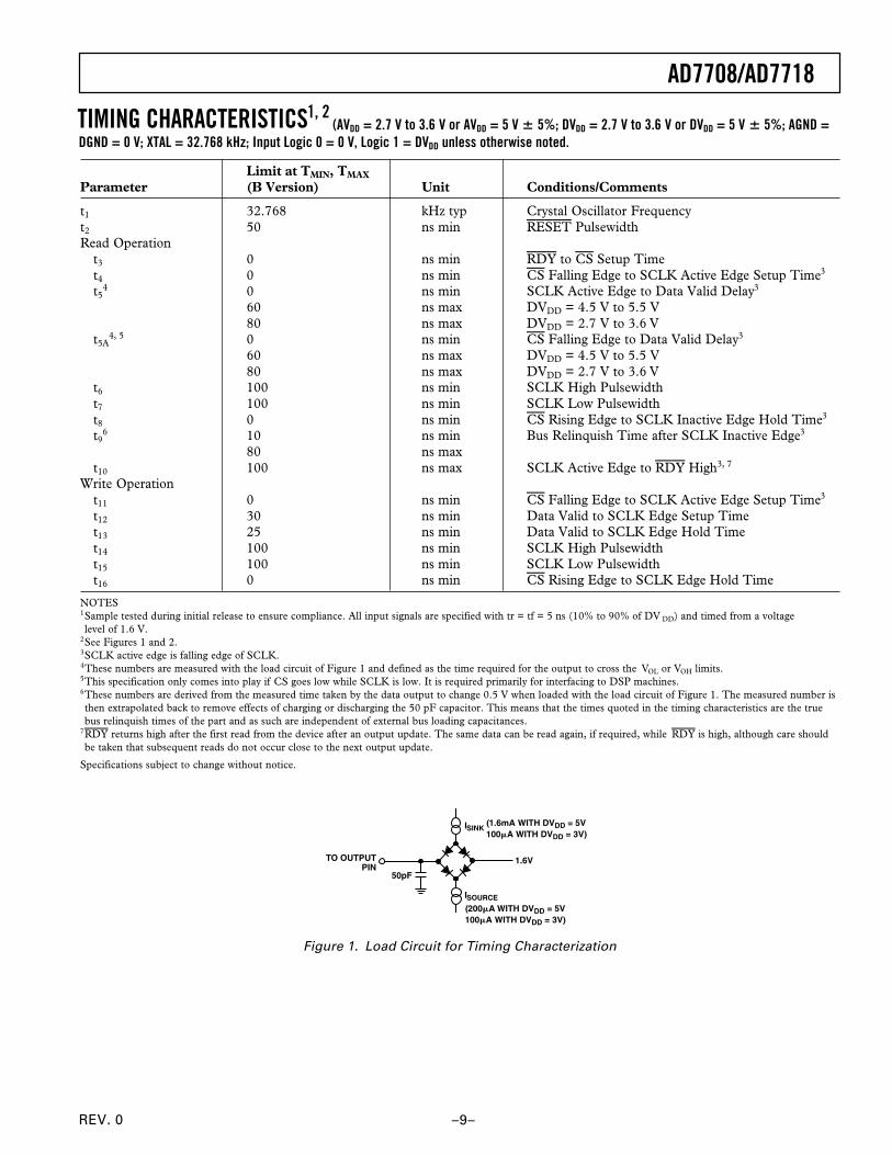
AD7708/AD7718PIN FUNCTION DESCRIPTIONS
Pin No Mnemonic Function
1 AIN7 Analog Input Channel 7. Programmable-gain analog input that can be used as a pseudo-differential input when used with AINCOM, or as the positive input of a fully-differential inputpair when used with AIN8. (See ADC Control Register section.)
2 AIN8 Analog Input Channel 8. Programmable-gain analog input that can be used as a pseudo-differential input when used with AINCOM, or as the negative input of a fully-differential inputpair when used with AIN7. (See ADC Control Register section.)
3 AVDD Analog Supply Voltage4 AGND Analog Ground5 REFIN1(–) Negative Reference Input. This reference input can lie anywhere between AGND and AVDD – 1 V.6 REFIN1(+) Positive reference input. REFIN(+) can lie anywhere between AVDD and AGND. The nominal
reference voltage [REFIN(+)–REFIN(–)] is 2.5 V but the part is functional with a referencerange from 1 V to AVDD.
7 AIN1 Analog Input Channel 1. Programmable-gain analog input that can be used as a pseudo-differential input when used with AINCOM, or as the positive input of a fully-differential inputpair when used with AIN2. (See ADC Control Register Section.)
8 AIN2 Analog Input Channel 2. Programmable-gain analog input that can be used as a pseudo-differential input when used with AINCOM, or as the negative input of a fully-differential inputpair when used with AIN1. (See ADC Control Register section.)
9 AIN3 Analog Input Channel 3. Programmable-gain analog input that can be used as a pseudo-differential input when used with AINCOM, or as the positive input of a fully-differential inputpair when used with AIN4. (See ADC Control Register section.)
10 AIN4 Analog Input Channel 4. Programmable-gain analog input that can be used as a pseudo-differential input when used with AINCOM, or as the negative input of a fully-differential inputpair when used with AIN3. (See ADC Control Register section.)
11 AIN5 Analog Input Channel 5. Programmable-gain analog input that can be used as a pseudo-differential input when used with AINCOM, or as the positive input of a fully-differential inputpair when used with AIN6. (See ADC Control Register section ADCCON.)
12 AINCOM All analog inputs are referenced to this input when configured in pseudo-differential input mode.13 REFIN2(+)/AIN9 Positive reference input/analog input. This input can be configured as a reference input with the
same characteristics as REFIN1(+) or as an additional analog input. When configured as ananalog input this pin provides a programmable-gain analog input that can be used as a pseudo-differential input when used with AINCOM, or as the positive input of a fully-differential inputpair when used with AIN10. (See ADC Control Register section.)
14 REFIN2(–)/AIN10 Negative reference input/analog input. This pin can be configured as a reference or analog input.When configured as a reference input it provides the negative reference input for REFIN2.When configured as an analog input it provides a programmable-gain analog input that can beused as a pseudo-differential input when used with AINCOM, or as the negative input of a fully-differential input pair when used with AIN9. (See ADC Control Register section.)
15 AIN6 Analog Input Channel 6. Programmable-gain analog input that can be used as a pseudo-differential input when used with AINCOM, or as the negative input of a fully-differential inputpair when used with AIN5. (See ADC Control Register section.)
16 P2 P2 can act as a general-purpose Input/Output bit referenced between AVDD and AGND. Thereis a weak pull-up to AVDD internally on this pin.
17 AGND It is recommended that this pin be tied directly to AGND.18 P1 P1 can act as a general-purpose Input/Output bit referenced between AVDD and AGND. There
is a weak pull-up to AVDD internally on this pin.19 RESET Digital input used to reset the ADC to its power-on-reset status. This pin has a weak pull-up
internally to DVDD.20 SCLK Serial clock input for data transfers to and from the ADC. The SCLK has a Schmitt-trigger
input making an opto-isolated interface more robust. The serial clock can be continuous with alldata transmitted in a continuous train of pulses. Alternatively, it can be a noncontinuous clockwith the information being transmitted to or from the AD7708/AD7718 in smaller batches of data.
REV. 0
AD7708/AD7718
–13–
Pin No Mnemonic Function
21 CS Chip Select Input. This is an active low logic input used to select the AD7708/AD7718. CS canbe used to select the AD7708/AD7718 in systems with more than one device on the serial bus oras a frame synchronization signal in communicating with the device. CS can be hardwired low,allowing the AD7708/AD7718 to be operated in 3-wire mode with SCLK, DIN, and DOUTused to interface with the device.
22 RDY RDY is a logic low status output from the AD7708/AD7718. RDY is low when valid data existsin the data register for the selected channel. This output returns high on completion of a readoperation from the data register. If data is not read, RDY will return high prior to the next updateindicating to the user that a read operation should not be initiated. The RDY pin also returnslow following the completion of a calibration cycle. RDY does not return high after a calibrationuntil the mode bits are written to enabling a new conversion or calibration.
23 DOUT Serial data output with serial data being read from the output shift register of the ADC. The outputshift register can contain data from any of the on-chip data, calibration or control registers.
24 DIN Serial Data Input with serial data being written to the input shift register on the AD7708/AD7718Data in this shift register is transferred to the calibration or control registers within the ADCdepending on the selection bits of the Communications register.
25 DGND Ground Reference Point for the Digital Circuitry.26 DVDD Digital Supply Voltage, 3 V or 5 V Nominal.27 XTAL2 Output from the 32 kHz Crystal Oscillator or Resonator Inverter.28 XTAL1 Input to the 32 kHz Crystal Oscillator or Resonator Inverter.
PIN CONFIGURATION
14
13
12
11
17
16
15
20
19
18
10
9
8
1
2
3
4
7
6
5
TOP VIEW(Not to Scale)
28
27
26
25
24
23
22
21
AD7708/AD7718
AIN7
DGND
DVDD
XTAL2
XTAL1
AIN8
AVDD
AGND
RDY
DOUT
DINREFIN1(–)
REFIN1(+)
AIN1
AIN2
AIN3
AIN4 RESET
SCLK
CS
AIN5
AINCOM
REFIN2(+)/AIN9
REFIN2(–)/AIN10
P1
AIN6
P2
AGND

REV. 0–14–
AD7708/AD7718
READING NUMBER
8389600
8389400
83880000 1000100
CO
DE
RE
AD
200 300
8389200
400 500 600 700 800 900
8389000
8388800
8388600
8388400
8388200
AVDD = DVDD = 5VINPUT RANGE = 20mV
REFIN1(+)–REFIN1(–) = 2.5VUPDATE RATE = 19.79Hz
TA = 25CVREF = 2.5VRMS NOISE = 0.58V rms
TPC 1. AD7718 Typical Noise Plot on ±20 mV Input Rangewith 19.79 Hz Update Rate
8
7
0
8388
039
8388
721
8388
687
8388
657
8388
615
8388
579
8388
547
8388
499
8388
449
8388
382
8388
754
8389
110
8389
033
8388
985
8388
941
8388
906
8388
874
8388
841
8388
805
8388
779
6
5
4
3
2
1
9
TPC 2. AD7718 Noise Distribution Histogram
2.5
01.0 3.02.52.01.5 3.5 5.04.54.0
2.0
1.5
1.0
0.5
3.0
VREF – V
RM
S N
OIS
E –
V
20mV RANGE
2.56V RANGE
AVDD = DVDD = 5VVREF = 2.5VINPUT RANGE = 2.56VUPDATE RATE = 19.79HzTA = 25C
TPC 3. RMS Noise vs. Reference Input(AD7718 andAD7708)
160 40302010 50 10090807060
24
22
20
18
26
UPDATE RATE – Hz
NO
MIS
SIN
G C
OD
ES
– M
in
110
CHOP = 0
TPC 4. AD7718 No-Missing Codes Performance
32767
1000 200 400300
32771
32770
32769
32768
32772
READING NUMBER
CO
DE
RE
AD
500
32766
32765
32764600 700 800 900 1000
AVDD = DVDD = 5VINPUT RANGE = 20mVUPDATE RATE = 19.79Hz
VREF = 2.5VTA = 25 C
TPC 5. AD7708 Typical Noise Plot on ±20 mV Input Range
200
3276732766 32768 3277032769
600
500
400
300
700
CODE
OC
CU
RR
EN
CE
32771
100
0
TPC 6. AD7708 Noise Histogram
–Typical Performance Characteristics

REV. 0
AD7708/AD7718
–15–
ADC CIRCUIT INFORMATIONThe AD7708/AD7718 incorporates a 10-channel multiplexerwith a sigma-delta ADC, on-chip programmable gain amplifierand digital filtering intended for the measurement of widedynamic range, low frequency signals such as those in weigh-scale,strain-gauge, pressure transducer, or temperature measurementapplications. The AD7708 offers 16-bit resolution while theAD7718 offers 24-bit resolution. The AD7718 is a pin-for-pincompatible version of the AD7708. The AD7718 offers a directupgradable path from a 16-bit to a 24-bit system without requiringany hardware changes and only minimal software changes.
These parts can be configured as four/five fully-differentialinput channels or as eight/ten pseudo-differential input chan-nels referenced to AINCOM. The channel is buffered and canbe programmed for one of eight input ranges from ±20 mV to±2.56 V. Buffering the input channel means that the part canhandle significant source impedances on the analog input andthat R, C filtering (for noise rejection or RFI reduction) can beplaced on the analog inputs if required. These input channelsare intended to convert signals directly from sensors without theneed for external signal conditioning.
The ADC employs a sigma-delta conversion technique to realizeup to 24 bits of no missing codes performance. The sigma-deltamodulator converts the sampled input signal into a digital pulsetrain whose duty cycle contains the digital information. A Sinc3
programmable low-pass filter is then employed to decimate themodulator output data stream to give a valid data conversion resultat programmable output rates. The signal chain has two modesof operation, CHOP enabled and CHOP disabled. The CHOP bitin the mode register enables and disables the chopping scheme.
Signal Chain Overview (CHOP Enabled, CHOP = 0)With CHOP = 0, chopping is enabled, this is the default and givesoptimum performance in terms of drift performance. With choppingenabled, the available output rates vary from 5.35 Hz (186.77 ms)to 105.03 Hz (9.52 ms). A block diagram of the ADC inputchannel with chop enabled is shown in Figure 4.
The sampling frequency of the modulator loop is many timeshigher than the bandwidth of the input signal. The integrator inthe modulator shapes the quantization noise (which results fromthe analog-to-digital conversion) so that the noise is pushedtoward one-half of the modulator frequency. The output of thesigma-delta modulator feeds directly into the digital filter. Thedigital filter then band-limits the response to a frequency signifi-cantly lower than one-half of the modulator frequency. In thismanner, the 1-bit output of the comparator is translated into aband limited, low noise output from the AD7708/AD7718 ADC.The AD7708/AD7718 filter is a low-pass, Sinc3 or (sinx/x)3
filter whose primary function is to remove the quantization noiseintroduced at the modulator. The cutoff frequency and deci-mated output data rate of the filter are programmable via the SFword loaded to the filter register. The complete signal chain ischopped resulting in excellent dc offset and offset drift specifica-tions and is extremely beneficial in applications where drift, noiserejection, and optimum EMI rejection are important factors.With chopping, the ADC repeatedly reverses its inputs. Thedecimated digital output words from the Sinc3 filters, therefore,have a positive offset and negative offset term included. As aresult, a final summing stage is included so that each outputword from the filter is summed and averaged with the previousfilter output to produce a new valid output result to be writtento the ADC data register. The programming of the Sinc3 deci-mation factor is restricted to an 8-bit register SF, the actualdecimation factor is the register value times 8. The decimatedoutput rate from the Sinc3 filter (and the ADC conversion rate)will therefore be
f
SFfADC MOD= ×
××1
31
8
where
fADC in the ADC conversion rate.
SF is the decimal equivalent of the word loaded to the filterregister.
fMOD is the modulator sampling rate of 32.768 kHz.
The chop rate of the channel is half the output data rate:
ff
CHOPADC
=×
12
As shown in the block diagram, the Sinc3 filter outputs alter-nately contain +VOS and –VOS, where VOS is the respectivechannel offset. This offset is removed by performing a runningaverage of two. This average by two means that the settling timeto any change in programming of the ADC will be twice thenormal conversion time, while an asynchronous step change onthe analog input will not be fully reflected until the third subse-quent output.
t
ftSETTLE
ADCADC= = ×2
2
The allowable range for SF is 13 to 255 with a default of 69(45H). The corresponding conversion rates, conversion times,and settling times are shown in Table I. Note that the conver-sion time increases by 0.732 ms for each increment in SF.
SINC 3 FILTER
MUX BUF PGA-
MOD0XORANALOG
INPUTDIGITALOUTPUT
18 SF
3
(8 SF )3 12
AIN + VOSAIN – VOS
fCHOP fIN fMOD fCHOP fADC
( (
Figure 4. ADC Channel Block Diagram with CHOP Enabled

REV. 0–16–
AD7708/AD7718Table I. ADC Conversion and Settling Times for VariousSF Words with CHOP = 0
SF Data Update Rate Settling TimeWord fADC (Hz) tSETTLE (ms)
13 105.3 19.0423 59.36 33.6927 50.56 39.5545 30.3 65.969 (Default) 19.79 101.0791 15 133.1182 7.5 266.6255 5.35 373.54
The overall frequency response is the product of a sinc3 and asinc response. There are sinc3 notches at integer multiples of3 × fADC and there are sinc notches at odd integer multiplesof fADC/2. The 3 dB frequency for all values of SF obeys thefollowing equation:
f (3 dB) = 0.24 × fADC
Normal-mode rejection is the major function of the digital filteron the AD7708/AD7718. The normal mode 50 ±1 Hz rejectionwith an SF word of 82 is typically –100 dB. The 60 ± 1 Hzrejection with SF = 68 is typically –100 dB. Simultaneous 50 Hzand 60 Hz rejection of better than 60 dB is achieved with an SFof 69. Choosing an SF word of 69 places notches at both 50 Hzand 60 Hz. Figures 5 to 9 show the filter rejection for a selectionof SF words.
The frequency response of the filter H (f) is as follows:
18
8 12
23
SFSF f f
f ff f
f fMOD
MOD
OUT
OUT×× × × ×
×
× × × ××
sin ( / )sin ( / )
sin ( / )sin ( / )
ππ
ππ
where
fMOD = 32,768 Hz,SF = value programmed into SF Register,fOUT = fMOD/(SF × 8 × 3).
The following plots show the filter frequency response for avariety of update rates from 5 Hz to 105 Hz.
FREQUENCY – Hz
0
–140
–2000 65050 100 150 200 250 300 350 400 450 500 550 600 700
AT
TE
NU
AT
ION
– d
B
–20
–120
–160
–180
–60
–100
–40
–80
SF = 13OUTPUT DATA RATE = 105HzINPUT BANDWIDTH = 25.2HzFIRST NOTCH = 52.5Hz50Hz REJECTION = –23.6dB, 50Hz1Hz REJECTION = –20.5dB60Hz REJECTION = –14.6dB, 60Hz1Hz REJECTION = –13.6dB
Figure 5. Filter Profile with SF = 13
FREQUENCY – Hz
0
–80
–1600 10010
AT
TE
NU
AT
ION
– d
B
20 30 40 50 60 70 80 90
–20
–40
–120
–140
–60
–100
SF = 82OUTPUT DATA RATE = 16.65HzINPUT BANDWIDTH = 4Hz50Hz REJECTION = –171dB, 50Hz1Hz REJECTION = –100dB60Hz REJECTION = –58dB, 60Hz1Hz REJECTION = –53dB
Figure 6. Filter Profile with SF = 82

REV. 0
AD7708/AD7718
–17–
FREQUENCY – Hz
0
–80
–1600 10010
AT
TE
NU
AT
ION
– d
B
20 30 40 50 60 70 80 90
–20
–40
–120
–140
–60
–100
SF = 255OUTPUT DATA RATE = 5.35HzINPUT BANDWIDTH = 1.28Hz50Hz REJECTION = –93dB, 50Hz1Hz REJECTION = –93dB60Hz REJECTION = –74dB, 60Hz1Hz REJECTION = –68dB
Figure 7. Filter Profile with SF = 255
FREQUENCY – Hz
0
–80
–1600 10010
AT
TE
NU
AT
ION
– d
B
20 30 40 50 60 70 80 90
–20
–40
–120
–140
–60
–100
SF = 69OUTPUT DATA RATE = 19.8HzINPUT BANDWIDTH = 4.74HzFIRST NOTCH = 9.9Hz50Hz REJECTION = –66dB, 50Hz1Hz REJECTION = –60dB60Hz REJECTION = –117dB, 60Hz1Hz REJECTION = –94dB
Figure 8. Filter Profile with Default SF = 69 Giving FilterNotches at Both 50 Hz and 60 Hz
FREQUENCY – Hz
0
–80
–1600 10010
AT
TE
NU
AT
ION
– d
B
20 30 40 50 60 70 80 90
–20
–40
–120
–140
–60
–100
SF = 68OUTPUT DATA RATE = 20.07HzINPUT BANDWIDTH = 4.82Hz50Hz REJECTION = –74dB, 50Hz1Hz REJECTION = –54.6dB60Hz REJECTION = –147dB, 60Hz1Hz REJECTION = –101dB
Figure 9. Filter Profile with SF = 68
ADC NOISE PERFORMANCE CHOP ENABLED(CHOP = 0)Tables II to V show the output rms noise and output peak-to-peak resolution in bits (rounded to the nearest 0.5 LSB) for aselection of output update rates. The numbers are typical andgenerated at a differential input voltage of 0 V with AVDD =DVDD = 5 V and using a 2.5 V reference. The output updaterate is selected via the SF7–SF0 bits in the Filter Register. It isimportant to note that the peak-to-peak resolution figures repre-sent the resolution for which there will be no code flicker withina six-sigma limit. The output noise comes from two sources. Thefirst is the electrical noise in the semiconductor devices (devicenoise) used in the implementation of the modulator. Secondly,when the analog input is converted into the digital domain,quantization noise is added. The device noise is at a low leveland is independent of frequency. The quantization noise starts atan even lower level but rises rapidly with increasing frequency tobecome the dominant noise source. The numbers in the tablesare given for the bipolar input ranges. For the unipolar rangesthe rms noise numbers will be the same as the bipolar range, butthe peak-to-peak resolution is now based on half the signal rangewhich effectively means losing one bit of resolution.

REV. 0–18–
AD7708/AD7718Table II. Typical Output RMS Noise vs. Input Range and Update Rate for AD7718 with Chop Enabled (CHOP = 0);Output RMS Noise in V
SF Data Update Input RangeWord Rate (Hz) 20 mV 40 mV 80 mV 160 mV 320 mV 640 mV 1.28 V 2.56 V
13 105.3 1.50 1.50 1.60 1.75 3.50 4.50 6.70 11.7523 59.36 1.0 1.02 1.06 1.15 1.22 1.77 3.0 5.0827 50.56 0.95 0.95 0.98 1.00 1.10 1.66 5.069 19.79 0.60 0.65 0.65 0.65 0.65 0.95 1.40 2.30255 5.35 0.35 0.35 0.37 0.37 0.37 0.51 0.82 1.25
Table III. Peak-to-Peak Resolution vs. Input Range and Update Rate for AD7718 with Chop Enabled (CHOP = 0);Peak-to-Peak Resolution in Bits
SF Data Update Input RangeWord Rate (Hz) 20 mV 40 mV 80 mV 160 mV 320 mV 640 mV 1.28 V 2.56 V
13 105.3 12 13 14 15 15 15.5 16 1623 59.36 12.5 13.5 14.5 15 16 17 17 1727 50.56 12.5 13.5 14.5 15.5 16.5 17 17 1769 19.79 13 14 15 16 17 17.5 18 18.5255 5.35 14 15 16 17 18 18.5 18.8 19.2
Table IV. Typical Output RMS Noise vs. Input Range and Update Rate for AD7708 with Chop Enabled (CHOP = 0);Output RMS Noise in V
SF Data Update Input RangeWord Rate (Hz) 20 mV 40 mV 80 mV 160 mV 320 mV 640 mV 1.28 V 2.56 V
13 105.3 1.50 1.50 1.60 1.75 3.50 4.50 6.70 11.7523 59.36 1.0 1.02 1.06 1.15 1.22 1.77 3.0 5.0827 50.56 0.95 0.95 0.98 1.00 1.10 1.66 5.069 19.79 0.60 0.65 0.65 0.65 0.65 0.95 1.40 2.30255 5.35 0.35 0.35 0.37 0.37 0.37 0.51 0.82 1.25
Table V. Peak-to-Peak Resolution vs. Input Range and Update Rate for AD7708 with Chop Enabled (CHOP = 0);Peak-to-Peak Resolution in Bits
SF Data Update Input RangeWord Rate (Hz) 20 mV 40 mV 80 mV 160 mV 320 mV 640 mV 1.28 V 2.56 V
13 105.3 12 13 14 15 15 15.5 16 1623 59.35 12.5 13.5 14.5 15 16 16 16 1627 50.56 12.5 13.5 14.5 15.5 16 16 16 1669 19.79 13 14 15 16 16 16 16 16255 5.35 14 15 16 16 16 16 16 16

REV. 0
AD7708/AD7718
–19–
SIGNAL CHAIN OVERVIEW CHOP DISABLED(CHOP = 1)
With CHOP =1 chopping is disabled. With chopping disabledthe available output rates vary from 16.06 Hz (62.26 ms) to1365.33 Hz (0.73 ms). The range of applicable SF words is from3 to 255. When switching between channels with chop disabled,the channel throughput is increased by a factor of two over thecase where chop is enabled. When used in multiplexed applica-tions operation with chop disabled will offer the best throughputtime when cycling through all channels. The drawback withchop disabled is that the drift performance is degraded andcalibration is required following a gain change or significanttemperature change. A block diagram of the ADC inputchannel with chop disabled is shown in Figure 10. Thesignal chain includes a mux, buffer, PGA, sigma-delta modu-lator, and digital filter. The modulator bit stream is applied toa Sinc3 filter. The programming of the Sinc3 decimationfactor is restricted to an 8-bit register SF, the actual decima-tion factor is the register value times 8. The decimated outputrate from the Sinc3 filter (and the ADC conversion rate) will there-fore be:
f
fSF
ADCMOD=×8
where
fADC is the ADC conversion rate,SF is the decimal equivalent of the word loaded to the filterregister, valid range is from 3 to 255,fMOD is the modulator sampling rate of 32.768 kHz.
The settling time to a step input is governed by the digital filter.A synchronized step change will require a settling time of threetimes the programmed update rate, a channel change can betreated as a synchronized step change. An unsynchronized stepchange will require four outputs to reflect the new analog inputat its output.
t
ftSETTLE
ADCADC= = ×3
3
The allowable range for SF is 3 to 255 with a default of 69(45H). The corresponding conversion rates, conversion times,and settling times are shown in Table VI. Note that the conver-sion time increases by 0.245 ms for each increment in SF.
Table VI. ADC Conversion and Settling Times for VariousSF Words with CHOP = 1
SF Data Update Rate Settling TimeWord fADC (Hz) tSETTLE (ms)
03 1365.33 2.2068 60.2 49.869 (Default) 59.36 50.5475 54.6 54.9382 49.95 60151 27.13 110.6255 16.06 186.76
The frequency response of the digital filter H (f) is as follows:
18
83
SFSF f f
f fMOD
MOD×× × × ×
×
sin( / )sin( / )
ππ
where
fMOD = 32,768 Hz,SF = value programmed into SF SFR.
The following shows plots of the filter frequency response usingdifferent SF words for output data rates of 16 Hz to 1.36 kHz.
There are sinc3 notches at integer multiples of the update rate.The 3 dB frequency for all values of SF obeys the followingequation:
f (3 dB) = 0.262 × fADC
The following plots show frequency response of the AD7708/AD7718 digital filter for various filter words. The AD7708/AD7718 are targeted at multiplexed applications. One of thekey requirements in these applications is to optimize the SFword to obtain the maximum filter rejection at 50 Hz and 60 Hzwhile minimizing the channel throughput rate. Figure 12 showsthe AD7708/AD7718 optimized throughput while maximizing50 Hz and 60 Hz rejection. This is achieved with an SF word of75. In Figure 13, by using a higher SF word of 151, 50 Hz and60 Hz rejection can be maximized at 60 dB with a channelthroughput rate of 110 ms. An SF word of 255 gives maximumrejection at both 50 Hz and 60 Hz but the channel throughputrate is restricted to 186 ms as shown in Figure 14.
SINC3 FILTERMUX BUF PGA-
MOD0
ANALOG INPUT
DIGITALOUTPUT
fIN fMOD fADC
Figure 10. ADC Channel Block Diagram with CHOP Disabled

REV. 0–20–
AD7708/AD7718
FREQUENCY – Hz
0
–80
–160
0 10010
AT
TE
NU
AT
ION
– d
B
20 30 40 50 60 70 80 90
–20
–40
–120
–140
–60
–100
SF = 68OUTPUT DATA RATE = 60.2HzSETTLING TIME = 49.8msINPUT BANDWIDTH = 15.5Hz50Hz REJECTION = –43dB, 50Hz1Hz REJECTION = –40dB60Hz REJECTION = –147dB, 60Hz1Hz REJECTION = –101dB
–200
–180
Figure 11. Frequency Response Operating with theSF Word of 68
FREQUENCY – Hz
0
–80
–160
0 10010
AT
TE
NU
AT
ION
– d
B
20 30 40 50 60 70 80 90
–20
–40
–120
–140
–60
–100
SF = 75OUTPUT DATA RATE = 54.6HzSETTLING TIME = 55msINPUT BANDWIDTH = 14.3Hz50Hz REJECTION = –62.5dB, 50Hz1Hz REJECTION = –57dB60Hz REJECTION = –63dB, 60Hz1Hz REJECTION = –60dB
–200
–180
Figure 12. Optimizing Filter Response for Throughputwhile Maximizing the Simultaneous 50 Hz and 60 HzRejection
FREQUENCY – Hz
0
–80
–160
0 10010
AT
TE
NU
AT
ION
– d
B
20 30 40 50 60 70 80 90
–20
–40
–120
–140
–60
–100
SF = 151OUTPUT DATA RATE = 27.12HzSETTLING TIME = 110msINPUT BANDWIDTH = 27.12Hz50Hz REJECTION = –65.4dB, 50Hz1Hz REJECTION = –60dB60Hz REJECTION = –63dB, 60Hz1Hz REJECTION = –60dB
–200
–180
Figure 13. Optimizing Filter Response for MaximumSimultaneous 50 Hz and 60 Hz Rejection
FREQUENCY – Hz
0
–80
–160
0 10010
AT
TE
NU
AT
ION
– d
B
20 30 40 50 60 70 80 90
–20
–40
–120
–140
–60
–100
SF = 255OUTPUT DATA RATE = 16.06HzSETTLING TIME = 186msINPUT BANDWIDTH = 4.21Hz50Hz REJECTION = –87dB, 50Hz1Hz REJECTION = –77dB60Hz REJECTION = –72dB, 60Hz1Hz REJECTION = –68dB
–200
–180
Figure 14. Frequency with Maximum SF Word = 255
ADC NOISE PERFORMANCE CHOP DISABLED(CHOP = 1)Tables VII to X show the output rms noise and output peak-to-peak resolution in bits (rounded to the nearest 0.5 LSB) forsome typical output update rates. The numbers are typical andgenerated at a differential input voltage of 0 V. The output updaterate is selected via the SF7–SF0 bits in the Filter Register. It isimportant to note that the peak-to-peak resolution figures representthe resolution for which there will be no code flicker within asix-sigma limit. The output noise comes from two sources. Thefirst is the electrical noise in the semiconductor devices (devicenoise) used in the implementation of the modulator. Secondly,
when the analog input is converted into the digital domain,quantization noise is added. The device noise is at a low leveland is independent of frequency. The quantization noise startsat an even lower level but rises rapidly with increasing frequencyto become the dominant noise source. The numbers in thetables are given for the bipolar input ranges. For the unipolarranges the rms noise numbers will be the same as the bipolarrange, but the peak-to-peak resolution is now based on half thesignal range which effectively means losing 1 bit of resolution.

REV. 0
AD7708/AD7718
–21–
Table VII. Typical Output RMS Noise vs. Input Range and Update Rate for AD7718 with Chop Disabled (CHOP = 1);Output RMS Noise in V
SF Data Update Input RangeWord Rate (Hz) 20 mV 40 mV 80 mV 160 mV 320 mV 640 mV 1.28 V 2.56 V
03 1365.33 30.31 29.02 58.33 112.7 282.44 361.72 616.89 166013 315.08 2.47 2.49 2.37 3.87 7.18 12.61 16.65 32.4566 62.06 0.743 0.852 0.9183 0.8788 0.8795 1.29 1.99 3.5969 59.38 0.961 0.971 0.949 0.922 0.923 1.32 2.03 3.7381 50.57 0.894 0.872 0.872 0.806 0.793 1.34 2.18 2.96255 16.06 0.475 0.468 0.434 0.485 0.458 0.688 1.18 1.78
Table VIII. Peak-to-Peak Resolution vs. Input Range and Update Rate for AD7718 with Chop Disabled (CHOP = 1);Peak-to-Peak Resolution in Bits
SF Data Update Input RangeWord Rate (Hz) 20 mV 40 mV 80 mV 160 mV 320 mV 640 mV 1.28 V 2.56 V
03 1365.33 8 9 9 9 9 9 9 913 315.08 11 12 14 14 14 14 15 1566 62.06 13 14 15 16 17 17 18 1869 59.36 13 14 15 16 17 17 18 1881 50.57 13 14 15 16 17 17 18 18255 16.06 14 15 16 17 18 18 19 19
Table IX. Typical Output RMS Noise vs. Input Range and Update Rate for AD7708 with Chop Disabled (CHOP = 1);Output RMS Noise in V
SF Data Update Input RangeWord Rate (Hz) 20 mV 40 mV 80 mV 160 mV 320 mV 640 mV 1.28 V 2.56 V
03 1365.33 30.31 29.02 58.33 112.7 282.44 361.72 616.89 166013 315.08 2.47 2.49 2.37 3.87 7.18 12.61 16.65 32.4566 62.06 0.743 0.852 0.9183 0.8788 0.8795 1.29 1.99 3.5969 59.38 0.961 0.971 0.949 0.922 0.923 1.32 2.03 3.7381 50.57 0.894 0.872 0.872 0.806 0.793 1.34 2.18 2.96255 16.06 0.475 0.468 0.434 0.485 0.458 0.688 1.18 1.78
Table X. Peak-to-Peak Resolution vs. Input Range and Update Rate for AD7708 with Chop Disabled (CHOP = 1);Peak-to-Peak Resolution in Bits
SF Data Update Input RangeWord Rate (Hz) 20 mV 40 mV 80 mV 160 mV 320 mV 640 mV 1.28 V 2.56 V
03 1365.33 8 9 9 9 9 9 9 913 315.08 11 12 14 14 14 14 15 1566 62.06 13 14 15 16 16 16 16 1669 59.36 13 14 15 16 16 16 16 1681 50.57 13 14 15 16 16 16 16 16255 16.06 14 15 16 16 16 16 16 16
REV. 0–22–
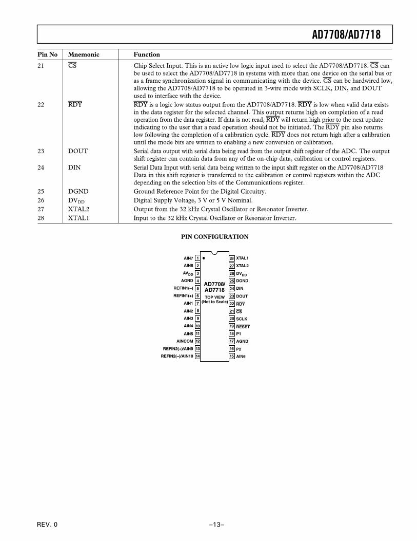
AD7708/AD7718ON-CHIP REGISTERSThe AD7708 and AD7718 are controlled and configured viaa number of on-chip registers which are shown in Figure 15.The first of these registers is the communications registerwhich is used to control all operations on these converters. Allcommunications with these parts must start with a write tothe communications register to specify the next operation tobe performed. After a power-on or RESET, the device defaultsto waiting for a write to the communications register. TheSTATUS register contains information pertaining to the operat-ing conditions of the converter. The STATUS register is a readonly register. The MODE register is used to configure the con-version mode, calibration, chop enable/disable, reference select,channel configuration and buffered or unbuffered operation onthe AINCOM analog input. The MODE register is a read/writeregister. The ADC Control register is a read/write register usedto select the active channel and program its input range andbipolar/unipolar operation. The I/O control register is a read/write register used to configure the operation of the 2-pin I/O
port. The filter register is a read/write register used to programthe data update rate of the converter. The ADC Data register isa read only register that contains the result of a data conversionon the selected channel. The ADC offset registers are read/writeregisters that contain the offset calibration data. There are fiveoffset registers, one for each of the fully differential input channels.When configured for pseudo-differential input mode the chan-nels share offset registers. The ADC gain registers are read/writeregisters that contain the gain calibration data. There are fiveADC gain registers, one for each of the fully differential inputchannels. When configured for pseudo differential input modethe channels share gain registers. The ADC contains Test registersfor factory use only, the user is advised not to alter the oper-ating conditions of these registers. The ID register is a read onlyregister and is used for silicon identification purposes. The follow-ing sections contains more in-depth detail on all of these registers.In the following descriptions, SET implies a Logic 1 state andCLEARED implies a Logic 0 state unless otherwise stated.
DOUT
DOUT
DOUTDIN
DOUTDIN
DOUTDIN
DOUTDIN
DOUT
DOUTDIN
DOUT
DOUT
WEN R/W 0 0 A1A2A3 A0
COMMUNICATIONS REGISTER
DOUT
DIN DIN
REGISTERSELECT
DECODER
ADC DATA REGISTER
STATUS REGISTER
MODE REGISTER
ADC CONTROL REGISTER
I/O CONTROL REGISTER
FILTER REGISTER
ID REGISTER
TEST REGISTER
ADC GAIN REGISTER
ADC OFFSET REGISTERDIN
DIN
Figure 15. On-Chip Registers

REV. 0
AD7708/AD7718
–23–
Table XI. Registers—Quick Reference Guide
Power-On/ResetRegister Name Type Size Default Value Function
Communications Write Only 8 Bits Not Applicable All operations to other registers are initiated throughthe Communications Register. This controls whethersubsequent operations are read or write operationsand also selects the register for that subsequentoperation.
Status Register Read Only 8 Bits 00 Hex Provides status information on conversions, calibra-tions and error conditions.
Mode Register Read/Write 8 Bits 00 Hex Controls functions such as mode of operation, chan-nel configuration, oscillator operation in power-down.
ADC (ADCCON)
Control Register Read/Write 8 Bits 07 Hex This register is used to select the active channelinput, configure the operating input range, and selectunipolar or bipolar operation.
I/O (IOCON)
I/O Control Register Read/Write 8 Bits 00 Hex This register is used to control and configure theI/O port.
Filter Register Read/Write 8 Bits 45 Hex This register determines the amount of averagingperformed by the sinc filter and consequently deter-mines the data update rate of the AD7708/AD7718.The filter register determines the update rate foroperation with CHOP enabled and CHOP disabled.
AD7718 ADC (DATA)Data Register Read Only 24 Bits 000000 Hex Provides the most up-to-date conversion result for
the selected channel on the AD7718.AD7708 (DATA)Data Register Read Only 16 Bits 0000 Hex Provides the most up-to-date conversion result for
the selected channel on the AD7708.
BSM BSL
YDR 0 LAC 0 RRE 0 0 KCOL
BSM BSL
3HC 2HC 1HC 0HC /U B 2NR 1NR 0NR
BSM BSL
7FS 6FS 5FS 4FS 3FS 2FS 1FS 0FS
BSM BSL
0 0 RID2P RID1P 0 0 TAD2P TAD1P
CR7 CR6 CR5 CR4 CR3 CR2 CR1 CR0
WEN R/W 0(0) 0(0) A3(0) A2(0) A1(0) A0(0)
MSB LSB
CHOP NEGBUF REFSEL CHCON OSCPD MD2 MD1 MD0

REV. 0–24–
AD7708/AD7718
Table XI. Registers—Quick Reference Guide (continued)
Power-On/ResetRegister Name Type Size Default Value Function
AD7718Offset Register Read/Write 24 Bits 800 000 Hex Contains a 24-bit word which is the offset calibration
coefficient for the part. The contents of this registerare used to provide offset correction on the outputfrom the digital filter. There are five Offset Registerson the part and these are associated with input chan-nels as outlined in the ADCCON register.
AD7718Gain Register Read/Write 24 Bits 5XXXX5 Hex Contains a 24-bit word which is the gain calibration
coefficient for the part. The contents of this registerare used to provide gain correction on the outputfrom the digital filter. There are five Gain Registerson the part and these are associated with input chan-nels as outlined in the ADCCON register.
AD7708Offset Register Read/Write 16 Bits 8000 Hex Contains a 16-bit word which is the offset calibration
coefficient for the part. The contents of this registerare used to provide offset correction on the outputfrom the digital filter. There are five Offset Registerson the part and these are associated with input chan-nels as outlined in the ADCCON register.
AD7708Gain Register Read/Write 16 Bits 5XXX Hex Contains a 16-bit word which is the gain calibration
coefficient for the part. The contents of this registerare used to provide gain correction on the outputfrom the digital filter. There are five Gain Registerson the part and these are associated with input chan-nels as outlined in the ADCCON register.
AD7708ID Register Read 8 Bits 5X Hex Contains an 8-bit byte which is the identifier for
the part.
AD7718ID Register Read 8 Bits 4X Hex Contains an 8-bit byte which is the identifier for
the part.
Test Registers Read/Write 16 Bits 0000 Hex Controls the test modes of the part that are usedwhen testing the part. The user is advised not tochange the contents of these registers.
REV. 0
AD7708/AD7718
–25–
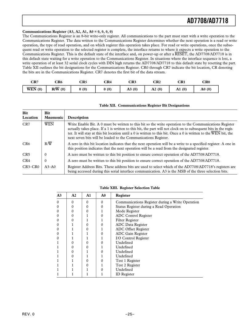
Communications Register (A3, A2, A1, A0 = 0, 0, 0, 0)The Communications Register is an 8-bit write-only register. All communications to the part must start with a write operation to theCommunications Register. The data written to the Communications Register determines whether the next operation is a read or writeoperation, the type of read operation, and on which register this operation takes place. For read or write operations, once the subse-quent read or write operation to the selected register is complete, the interface returns to where it expects a write operation to theCommunications Register. This is the default state of the interface and, on power-up or after a RESET, the AD7708/AD7718 is inthis default state waiting for a write operation to the Communications Register. In situations where the interface sequence is lost, awrite operation of at least 32 serial clock cycles with DIN high returns the AD7708/AD7718 to this default state by resetting the part.Table XII outlines the bit designations for the Communications Register. CR0 through CR7 indicate the bit location, CR denotingthe bits are in the Communications Register. CR7 denotes the first bit of the data stream.
7RC 6RC 5RC 4RC 3RC 2RC 1RC 0RC
NEW )0( /R W )0( )0(0 )0(0 )0(3A )0(2A )0(1A )0(0A
Table XII. Communications Register Bit Designations
Bit BitLocation Mnemonic Description
CR7 WEN Write Enable Bit. A 0 must be written to this bit so the write operation to the Communications Registeractually takes place. If a 1 is written to this bit, the part will not clock on to subsequent bits in the register. It will stay at this bit location until a 0 is written to this bit. Once a 0 is written to the WEN bit, thenext seven bits will be loaded to the Communications Register.
CR6 R/W A zero in this bit location indicates that the next operation will be a write to a specified register. A one inthis position indicates that the next operation will be a read from the designated register.
CR5 0 A zero must be written to this bit position to ensure correct operation of the AD7708/AD7718.
CR4 0 A zero must be written to this bit position to ensure correct operation of the AD7708/AD7718.
CR3–CR0 A3–A0 Register Address Bits. These address bits are used to select which of the AD7708/AD7718’s registers arebeing accessed during this serial interface communication. A3 is the MSB of the three selection bits.
Table XIII. Register Selection Table
A3 A2 A1 A0 Register
0 0 0 0 Communications Register during a Write Operation0 0 0 0 Status Register during a Read Operation0 0 0 1 Mode Register0 0 1 0 ADC Control Register0 0 1 1 Filter Register0 1 0 0 ADC Data Register0 1 0 1 ADC Offset Register0 1 1 0 ADC Gain Register0 1 1 1 I/O Control Register1 0 0 0 Undefined1 0 0 1 Undefined1 0 1 0 Undefined1 0 1 1 Undefined1 1 0 0 Test 1 Register1 1 0 1 Test 2 Register1 1 1 0 Undefined1 1 1 1 ID Register

REV. 0–26–
AD7708/AD7718Status Register (A3, A2, A1, A0 = 0, 0, 0, 0; Power-On-Reset = 00Hex)The ADC Status Register is an 8-bit read-only register. To access the ADC Status Register, the user must write to the Communica-tions Register selecting the next operation to be a read and load Bits A3-A0 with 0, 0, 0,0. Table XIV outlines the bit designationsfor the Status Register. SR0 through SR7 indicate the bit location, SR denoting the bits are in the Status Register. SR7 denotes thefirst bit of the data stream. The number in brackets indicates the power-on/reset default status of that bit.
RS 7 6RS 5RS 4RS 3RS 2RS 1RS 0RS
YDR )0( )0(0 )0(LAC )0(0 )0(RRE )0(0 )0(0 )0(KCOL
Table XIV. Status Register Bit Designations
Bit BitLocation Mnemonic Description
SR7 RDY Ready Bit for the ADCSet when data is transferred to the ADC data registers or on completion of calibration cycle. The RDYbit is cleared automatically a period of time before the data register is updated with a new conversionresult or after the ADC data register has been read. This bit is also cleared by a write to the mode bits toindicate a conversion or calibration. The RDY pin is the complement of the RDY bit.
SR6 0 Bit is automatically cleared. Reserved for future use
SR5 CAL Calibration Status BitSet to indicate completion of calibration. It is set at the same time that the RDY is set high.Cleared by a write to the mode bits to start another ADC conversion or calibration.
SR4 0 This bit is automatically cleared. Reserved for future use
SR3 ERR ADC Error BitSet to indicate that the result written to the ADC data register has been clamped to all zeros or all ones.After a calibration this bit also flags error conditions that caused the calibration registers not to bewritten. Error sources include Overrange.Cleared by a write to the mode bits to initiate a conversion or calibration.
SR2 0 This bit is automatically cleared. Reserved for future use
SR1 0 This bit is automatically cleared. Reserved for future use
SR0 LOCK PLL Lock Status Bit.Set if the PLL has locked onto the 32.768 kHz crystal oscillator clock. If the user is worried aboutexact sampling frequencies etc., the LOCK bit should be interrogated and the result discarded if theLOCK bit is zero.

REV. 0
AD7708/AD7718
–27–
Mode Register (A3, A2, A1, A0 = 0, 0, 0, 1; Power-On-Reset = 00Hex)The Mode Register is an 8-bit register from which data can be read or to which data can be written. This register configures theoperating modes of the AD7708/AD7718. Table XV outlines the bit designations for the Mode Register. MR7 through MR0 indi-cate the bit location, MR denoting the bits are in the Mode Register. MR7 denotes the first bit of the data stream. The number inbrackets indicates the power-on/reset default status of that bit.
7RM 6RM 5RM 4RM 3RM 2RM 1RM 0RM
POHC )0( )0(FUBGEN )0(LESFER )0(NOCHC )0(DPCSO )0(2DM )0(1DM )0(0DM
Table XV. Mode Register Bit Designations
Bit BitLocation Mnemonic Description
MR7 CHOP If this bit is cleared, chopping is enabled. When this bit is set chopping is disabled. The default is forchop enabled.
MR6 NEGBUF This bit controls the operation of the input buffer on the AINCOM input when a channel is config-ured for pseudo-differential mode of operation. If cleared, the analog negative input (AINCOM) isunbuffered allowing it to be tied to AGND in single-ended input configuration. If this bit is set theanalog negative input (AINCOM) is buffered, placing a restriction on its common-mode input range.
MR5 REFSEL If this bit is cleared, the reference selected is REFIN1(+) and REFIN1(–) for the active channel. Ifthis bit is set, the reference selected is REFIN2(+) and REFIN2(–) for the active channel. The con-tents of the CHCON bit overrides the REFSEL bit. If the ADC is configured in five fully-differentialor 10 pseudo-differential input channel mode, the REFSEL bit setting is irrelevant as only onereference input is available. VREF Select implemented using the REFSEL bit enables the user toperform both absolute and ratiometric measurements.
MR4 CHCON When cleared the device is configured as an 8-input channel converter, configured as eight pseudo-differential input channels with respect to AINCOM or four differential input arrangementswith two reference input selection options. When set the device is configured as a 10 pseudo-differential input or a five differential input channel arrangement with a single referenceinput option.
MR3 OSCPD Oscillator Power-Down Bit.If this bit is set, placing the AD7708/AD7718 in standby mode will stop the crystal oscillator reducingthe power drawn by these parts to a minimum. The oscillator will require 300 ms to begin oscillatingwhen the ADC is taken out of standby mode. If this bit is cleared, the oscillator is not shut off whenthe ADC is put into standby mode and will not require the 300 ms start-up time when the ADC istaken out of standby.
MR2–MR0 MD2–MD0 ADC Mode Bits.These bits select the operational mode of the ADC as follows:
MD2 MD1 MD00 0 0 Power-Down Mode (Power-On Default)0 0 1 Idle Mode
In Idle Mode the ADC filter and modulator are held in a reset state although the modulator clocksare still provided.
0 1 0 Single Conversion ModeIn Single Conversion Mode, a single conversion is performed on the enabled channels. On comple-tion of the conversion the ADC data registers are updated, the relevant flags in the STATUS registerare written, and idle mode is reentered with the MD2–MD0 being written accordingly to 001.
0 1 1 Continuous ConversionIn continuous conversion mode, the ADC data registers are regularly updated at the selected updaterate (see Filter register).
1 0 0 Internal Zero-Scale CalibrationInternal short automatically connected to the enabled channel(s)
1 0 1 Internal Full-Scale CalibrationExternal VREF is connected automatically to the ADC input for this calibration.
1 1 0 System Zero-Scale CalibrationUser should connect system zero-scale input to the channel input pins as selected by CH3–CH0 bitsin the control registers.
1 1 1 System Full-Scale CalibrationUser should connect system full-scale input to the channel input pins as selected by CH3–CH0 bitsin the control registers.

REV. 0–28–
AD7708/AD7718Operating Characteristics when Addressing the Mode and Control Registers1. Any change to the MD bits will immediately reset the ADCs. A write to the MD2–MD0 bits with no change is also treated as a reset.
2. Once the MODE has been written with a calibration mode, the RDY bit (STATUS) is immediately reset and the calibrationcommences. On completion the appropriate calibration registers are written, the bit in STATUS register is updated and theMD2–MD0 bits are reset to 001 to indicate the ADC is back in idle mode.
3. Calibrations are performed with the maximum allowable SF value with chop enabled. SF register is reset to user configurationafter calibration with chop enabled. Calibrations are performed with the selected value of SF when chop is disabled.
ADC Control Register (ADCCON): (A3, A2, A1, A0 = 0, 0, 1, 0; Power-On-Reset = 07 Hex)The ADC Control Register is an 8-bit register from which data can be read or to which data can be written. This register is used toconfigure the ADC for range, channel selection, and unipolar or bipolar coding. Table XVI outlines the bit designations for the ADCcontrol register ADCCON7 through ADCCON0 indicate the bit location, ADCCON denoting the bits are in the ADC ControlRegister. ADCCON7 denotes the first bit of the data stream. The number in brackets indicates the power-on/reset default status ofthat bit.
Table XVI. ADC Control Register (ADCCON) Bit Designations
Bit BitLocation Mnemonic Description
ADCCON7 CH3 ADC Channel Selection Bits. Written by the user to select either pseudo-differential or fully-ADCCON6 CH2 differential input pairs used by the ADC as follows:ADCCON5 CH1ADCCON4 CH0
8-Channel Configuration 10-Channel Configuration(CHCON = 0) (CHCON = 1)
Positive Negative Cal Register Positive Negative Cal RegisterCH3 CH2 CH1 CH0 Input Input Pair Input Input Pair0 0 0 0 AIN1 AINCOM 1 AIN1 AINCOM 10 0 0 1 AIN2 AINCOM 2 AIN2 AINCOM 20 0 1 0 AIN3 AINCOM 3 AIN3 AINCOM 30 0 1 1 AIN4 AINCOM 4 AIN4 AINCOM 40 1 0 0 AIN5 AINCOM 1 AIN5 AINCOM 50 1 0 1 AIN6 AINCOM 2 AIN6 AINCOM 10 1 1 0 AIN7 AINCOM 3 AIN7 AINCOM 20 1 1 1 AIN8 AINCOM 4 AIN8 AINCOM 31 0 0 0 AIN1 AIN2 1 AIN1 AIN2 11 0 0 1 AIN3 AIN4 2 AIN3 AIN4 21 0 1 0 AIN5 AIN6 3 AIN5 AIN6 31 0 1 1 AIN7 AIN8 4 AIN7 AIN8 41 1 0 0 AIN2 AIN2 1 AIN9 AIN10 51 1 0 1 AINCOM AINCOM 1 AINCOM AINCOM 11 1 1 0 REFIN(+) REFIN(–) 1 AIN9 AINCOM 41 1 1 1 OPEN OPEN 1 AIN10 AINCOM 5
ADCCON3 U/B Unipolar/Bipolar Bit.Set by user to enable unipolar coding i.e., zero differential input will result in 000000hexoutput and a full-scale differential input will result in FFFFFF Hex output when operated in24-bit mode.Cleared by user to enable bipolar coding, Negative full-scale differential input will result in anoutput code of 000000 Hex, zero differential input will result in an output code of 800000 Hexand a positive full-scale differential input will result in an output code of FFFFFF Hex.
ADCCON7 ADCCON6 ADCCON5 ADCCON4 ADCCON3 ADCCON2 ADCCON1 ADCCON0
CH3 (0) CH2 (0) CH1 (0) CH0 (0) U/B (0) RN2 (1) RN1 (1) RN0 (1)
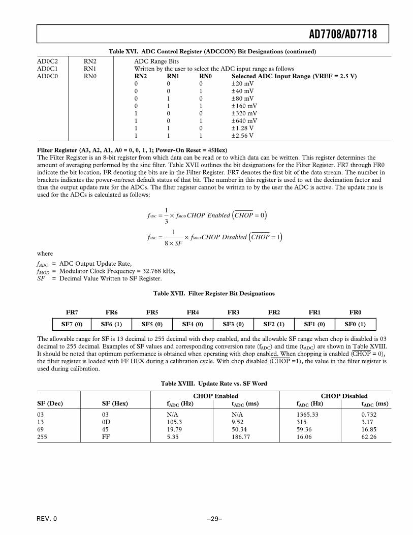
REV. 0
AD7708/AD7718
–29–
AD0C2 RN2 ADC Range BitsAD0C1 RN1 Written by the user to select the ADC input range as followsAD0C0 RN0 RN2 RN1 RN0 Selected ADC Input Range (VREF = 2.5 V)
0 0 0 ±20 mV0 0 1 ±40 mV0 1 0 ±80 mV0 1 1 ±160 mV1 0 0 ±320 mV1 0 1 ±640 mV1 1 0 ±1.28 V1 1 1 ±2.56 V
Filter Register (A3, A2, A1, A0 = 0, 0, 1, 1; Power-On Reset = 45Hex)The Filter Register is an 8-bit register from which data can be read or to which data can be written. This register determines theamount of averaging performed by the sinc filter. Table XVII outlines the bit designations for the Filter Register. FR7 through FR0indicate the bit location, FR denoting the bits are in the Filter Register. FR7 denotes the first bit of the data stream. The number inbrackets indicates the power-on/reset default status of that bit. The number in this register is used to set the decimation factor andthus the output update rate for the ADCs. The filter register cannot be written to by the user the ADC is active. The update rate isused for the ADCs is calculated as follows:
f f CHOP Enabled CHOP
fSF
f CHOP Disabled CHOP
ADC MOD
ADC MOD
= × =
=×
× =
( )
( )
1
30
1
81
where
fADC = ADC Output Update Rate,fMOD = Modulator Clock Frequency = 32.768 kHz,SF = Decimal Value Written to SF Register.
Table XVII. Filter Register Bit Designations
7RF 6RF 5RF 4RF 3RF 2RF 1RF 0RF
)0(7FS 6FS )1( 5FS )0( 4FS )0( 3FS )0( )1(2FS )0(1FS )1(0FS
The allowable range for SF is 13 decimal to 255 decimal with chop enabled, and the allowable SF range when chop is disabled is 03decimal to 255 decimal. Examples of SF values and corresponding conversion rate (fADC) and time (tADC) are shown in Table XVIII.It should be noted that optimum performance is obtained when operating with chop enabled. When chopping is enabled (CHOP = 0),the filter register is loaded with FF HEX during a calibration cycle. With chop disabled (CHOP =1), the value in the filter register isused during calibration.
Table XVIII. Update Rate vs. SF Word
CHOP Enabled CHOP DisabledSF (Dec) SF (Hex) fADC (Hz) tADC (ms) fADC (Hz) tADC (ms)
03 03 N/A N/A 1365.33 0.73213 0D 105.3 9.52 315 3.1769 45 19.79 50.34 59.36 16.85255 FF 5.35 186.77 16.06 62.26
Table XVI. ADC Control Register (ADCCON) Bit Designations (continued)

REV. 0–30–
AD7708/AD7718I/O Control Register (IOCON): (A3, A2, A1, A0 = 0, 1, 1, 1; Power-On-Reset = 00Hex)The IOCON Register is an 8-bit register from which data can be read or to which data can be written. This register is used to con-trol and configure the I/O port. Table XIX outlines the bit designations for this register. IOCON7 through IOCON0 indicate thebit location, IOCON denoting the bits are in the I/O Control Register. IOCON7 denotes the first bit of the data stream. The num-ber in brackets indicates the power-on/reset default status of that bit. A write to the IOCON register has immediate effect and doesnot reset the ADCs.
7NOCOI 6NOCOI 5NOCOI 4NOCOI 3NOCOI 2NOCOI 1NOCOI 0NOCOI
)0( 0 )0( )0(RID2P RID1P )0( 0 )0( )0(0 )0(TAD2P )0(TAD1P
Table XIX. IOCON (I/O Control Register) Bit Designations
Bit BitLocation Mnemonic Description
IOCON7 0 This bit should always be cleared. Reserved for future use.
IOCON6 0 This bit should always be cleared. Reserved for future use.
IOCON5 P2DIR P2, I/O Direction Control Bit.Set by user to enable P2 as an output.Cleared by user to enable P2 as an input. There are weak pull-ups internally when enabledas an input.
IOCON4 P1DIR P1, I/O Direction Control Bit.Set by user to enable P1 as an output.Cleared by user to enable P1 as an input. There are weak pull-ups internally when enabledas an input.
IOCON3 0 This bit should always be cleared. Reserved for future use.
IOCON2 0 This bit should always be cleared. Reserved for future use.
IOCON1 P2DAT Digital I/O Port (P1) Data Bit.The readback value of this bit indicates the status of the pin regardless of whether this pin isconfigured as an input or an output. The value written to this data bit will appear at theoutput port when the I/O pin is enabled as an output.
IOCON0 P1DAT Digital I/O port (P1) Data Bit.The readback value of this bit indicates the status of the pin, regardless of whether this pin isconfigured as an input or an output. The value written to this data bit will appear at theoutput port when the I/O pin is enabled as an output.
ADC Data Result Register (DATA): (A3, A2, A1, A0 = 0, 1, 0, 0; Power-On-Reset = 000000Hex)The conversion result for the selected ADC channel is stored in the ADC data register (DATA). This register is 16 bits wide on theAD7708 and 24 bits wide on the AD7718. This is a read only register. On completion of a read from this register the RDY bit inthe status register is cleared. These ADCs can be operated in either unipolar or bipolar mode of operation.
Unipolar ModeIn unipolar mode of operation the output coding is straight binary. With an analog input voltage of 0 V the output code is 0000Hexfor the AD7708 and 000000Hex for the AD7718. With an analog input voltage of 1.024 VREF/Gain the output code is FFFFHexfor the AD7708 and FFFFFF Hex for the AD7718. The output code for any analog input voltage can be represented as follows:
Code = (AIN × GAIN × 2N)/(1.024 × VREF)
where
AIN is the analog input voltage andN = 16 for the AD7708 and N = 24 for the AD7718.

REV. 0
AD7708/AD7718
–31–
Bipolar ModeWith an analog input voltage of (–1.024 VREF/GAIN), the output code is 0000 Hex using the AD7708 and 000000H using the AD7718.With an analog input voltage of 0 V, the output code is 8000Hex for the AD7708 and 800000Hex for the AD7718. With an analoginput voltage of (+1.024 VREF/GAIN), the output code is FFFF Hex for the AD7708 and FFFFFF Hex for the AD7718. Note theanalog inputs are pseudo bipolar inputs and the analog input voltage must remain within the common-mode input range at all times.The output code for any analog input voltage can be represented as follows:
Code = 2N–1 × [(AIN × GAIN/1.024 × VREF) + 1]
where
AIN is the analog input voltage,N = 16 for the AD7708, andN = 24 for the AD7718.
ADC Offset Calibration Coefficient Registers (OF0): (A3, A2, A1, A0 = 0, 1, 0, 1; Power-On-Reset = 8000(00)Hex)The offset calibration registers are 16-bit registers on the AD7708 and 24-bit registers on the AD7718. These registers hold the offsetcalibration coefficient for the ADC. The power-on-reset value of the internal zero-scale calibration coefficient registers is 8000(00).There are five offset registers available, one for each of the fully differential input channels. Calibration register pairs are shared whenoperating in pseudo-differential input mode. However, these bytes will be automatically overwritten if an internal or system zero-scalecalibration is initiated by the user via MD2–MD0 bits in the MODE register. The channel bits, in association with the communicationregister address for the OF0 register, allow access to this register. This register is a read/write register. The calibration register canonly be written to if the ADC is inactive (MD bits in the mode register = 000 or 001). Reading of the calibration register does notclear the RDY bit.
ADC Gain Calibration Coefficient Register (GNO): (A3, A2, A1, A0 = 0, 1, 1, 0; Power-On-Reset = 5XXX(X5) Hex)The gain calibration registers are 16-bit registers on the AD7708 and 24-bit registers on the AD7718. These registers are configuredat power-on with factory-calculated internal full-scale calibration coefficients. There are five full-scale registers available, one for eachof the fully differential input channels. Calibration register pairs are shared when operating in pseudo-differential input mode. Everydevice will have different default coefficients. However, these bytes will be automatically overwritten if an internal or system full-scalecalibration is initiated by the user via MD2–MD0 bits in the MODE register. The channel bits, in association with the communicationregister address, allow access to the data contained in the GN0 register. This is a read/write register. The calibration registers canonly be written to if the ADC is inactive (MD bits in the mode register = 000 or 001). Reading of the calibration registers does notclear the RDY bit. A calibration (self or system) is required when operating with chop mode disabled.
ID Register (ID): (A3, A2, A1, A0 = 1, 1, 1, 1; Power-On-Reset = 4X Hex (AD7718) and 5X Hex (AD7708)This register is a read only 8-bit register. The contents are used to determine the die revision of the silicon. Table XX indicates thebit locations for the AD7708.
Table XX. ID Register Bit Designation
User Nonprogrammable Test RegistersThe AD7708 and AD7718 contain two test registers. The bits in these test registers control the test modes of these ADCs which areused for the testing of the device. The user is advised not to change the contents of these registers.
ID7 ID6 ID5 ID4 ID3 ID2 ID1 ID0
0 1 0 0/1 X X X X

REV. 0–32–
AD7708/AD7718Configuring the AD7708/AD7718All user-accessible registers on the AD7708 and AD7718 areaccessed via the serial interface. Communication with any ofthese registers is initiated by first writing to the Communica-tions Register. Figures 16, 17, and 18 show flow diagrams forinitializing the ADC, a sequence for calibrating the ADC chan-nels, and a routine that cycles through and reads all channels.Figure 16 shows a flowchart detailing necessary programmingsteps required to initialize the ADC. The following are the generalprogramming steps required:
1. Configure and initialize the microcontroller or microprocessorserial port.
2. Initialize the AD7708/AD7718 by configuring the followingregisters:
a. IOCON to configure the digital I/O port.
b. FILTER to configure the update rate for each channel.
c. ADCCON to select the active input channel, selectthe analog input range, and select unipolar or bipolaroperation.
d. MODE to configure the operating mode. The moderegister selects chop or nonchop operation, buffered/unbuffered operation of the AINCOM input, 8-/10-channel mode of operation and reference select alongwith the selection of conversion, calibration or idlemodes of operation.
All operations consist of a write to the communications registerto specify the next operation as a write to a specified register.Data is then written to the specified register. When each sequenceis complete, the ADC defaults to waiting for another write tothe communications register to specify the next operation.
WRITE TO COMMUNICATIONS REGISTER SETTING UPNEXT OPERATION TO BE A WRITE TO THE MODEREGISTER. CALIBRATE AND SELECT MODE OFOPERATION
WRITE TO COMMUNICATIONS REGISTER SETTING UPNEXT OPERATION TO BE A WRITE TO THE ADCCONTROL REGISTER. CONFIGURE ADCCON
WRITE TO COMMUNICATIONS REGISTER SETTING UPNEXT OPERATION TO BE A WRITE TO THE FILTERREGISTER. SET SF WORD FOR REQUIREDUPDATE RATE
WRITE TO COMMUNICATIONS REGISTER SELECTINGNEXT OPERATION TO BE A WRITE TO THE IOCONREGISTER AND CONFIGURE THIS REGISTER
POWER-ON/RESET FOR AD7708/AD7718
CONFIGURE AND INITIALIZE C/P SERIAL PORT
START
Figure 16. Initializing AD7708/AD7718
END
CALANOTHERCHANNEL
WRITE TO MODE REGISTER SELECTINGFULL-SCALE CALIBRATION
WRITE TO MODE REGISTER SELECTINGZERO-SCALE CALIBRATION
WRITE TO ADCCON SELECTING CHANNEL AND CONFIGURINGINPUT RANGE AND UNIPOLAR/BIPOLAR MODE
CALIBRATION ROUTINE
MD BITS= 001?
NOYES
MD BITS= 001?
NOYES
YES
NO
Figure 17. Calibrating the AD7708/AD7718
Figure 17 shows a flowchart detailing necessary programmingsteps required when calibrating the AD7708/AD7718. TheAD7708/AD7718 have dedicated calibration register pairs foreach of the fully-differential input channels. Having a dedicatedregister pair per channel allows each channel to be calibrated aspart of the initialization and the ADC picks up the relevantcoefficients for each channel during normal operation. Whenoperating is pseudo-differential mode channels share calibrationregister pairs. Channels that share coefficients should be config-ured with the same operating conditions to avoid having tocalibrate each time a channel is switched, especially with chopmode disabled. The AD7708/AD7718 are factory-calibratedwith chop mode enabled and, therefore, if the ADC is operatedat the same conditions as the factory-calibration field calibra-tions will not be required. Extremely low offset error and offsetand gain drift errors are a by product of the chopping scheme.When operating with chop mode disabled, the user can achievefaster throughput times. An offset calibration is required withchop disabled when a gain or temperature change occurs. Thefollowing are the general programming steps required whencalibrating a channel on the AD7708/AD7718.

REV. 0
AD7708/AD7718
–33–
1. Write to the ADCCON register to select the channel to becalibrated, its input range, and operation in unipolar orbipolar mode.
2. Write to the mode register selecting chop or nonchop modeof operation, select the reference, buffered/unbuffered opera-tion on the AINCOM, and select zero-scale offset calibration.Zero-scale calibration can be either self-calibration, wherethe ADC determines the zero point internal to the ADC, or asystem calibration where the user must supply the zero-scalevoltage to the input for the duration of the calibration.
3. The calibration is initiated following the write to the moderegister. The user then needs to determine when the calibra-tion is complete. This can be performed in two ways, bypolling the RDY pin or flag or by monitoring the MD2,MD1, MD0 bits in the mode register. These bits are reset to0, 0, 1 when the calibration is complete. The flowchart usespolling of the mode bits in the mode register to determinewhen the calibration is complete.
4. The next step is to perform the full-scale calibration. Full-scalecalibration can be a self-calibration or system calibration.Using system calibration the user must supply the full-scalesignal to the analog inputs for the duration of the calibration.Again the MD2, MD1, MD0 bits in the mode register aremonitored to determine when the calibration is complete.
Figure 18 shows a flowchart detailing the necessary program-ming steps required to cycle through and read data results fromall channels in a multiplexed application. This flowchart assumesthat all channels have been previously calibrated. The followingare the general programming steps required when reading allchannels in a multiplexed application.
1. The AD7708/AD7718 is put into continuous conversionmode. In this mode the part continually converts on thespecified channel and the RDY line indicates when validdata is available to be read from the data register.
2. The ADCCON register is written to select the channelfor conversion, its input range and operation is unipolar/bipolar mode.
3. In this flowchart hardware polling of the RDY line is per-formed to determine when it is valid to read data from theconverter. When RDY is low, valid data is available in thedata register. The RDY line is set high on a channel changeand will not go low until a new valid data word is available.Alternatively, the RDY bit in the status register can be polledin software to determine when to read data from the converter.
4. When the data is read, increment the channel address pointerto select the next channel, poll the RDY pin, or RDY bit inthe status register, and again read the data. Continue until allchannels have been read.
POLL RDY PIN
WRITE TO ADCCON SELECTING CHANNEL NAND ITS OPERATING RANGE
END
WRITE TO COMMUNICATIONS REGISTER SETTING UPNEXT OPERATION TO BE A READ OF DATA REGISTERAND THEN READ DATA RESULT
WRITE TO MODE REGISTER SELECTINGCONTINUOUS CONVERSION MODE
CYCLE THROUGH ANDREAD ALL CHANNELS
RDYLOW?
NOYES
ALLCHANNELS
READ
NO
YES
INCREMENT CHANNEL ADDRESS (N = N+1)
Figure 18. Multichannel Read Operation

REV. 0–34–
AD7708/AD7718DIGITAL INTERFACEAs previously outlined, the AD7708/AD7718’s programmablefunctions are controlled using a set of on-chip registers. Data iswritten to these registers via the part’s serial interface and readaccess to the on-chip registers is also provided by this interface.All communications to the part must start with a write operationto the Communications Register. After power-on or RESET,the device expects a write to its Communications Register. Thedata written to this register determines whether the next operationto the part is a read or a write operation and also determines towhich register this read or write operation occurs. Therefore,write access to any of the other registers on the part starts with awrite operation to the Communications Register followed by awrite to the selected register. A read operation from any otherregister on the part (including the output data register) startswith a write operation to the Communications Register followedby a read operation from the selected register.
The AD7708/AD7718s serial interface consists of five signals,CS, SCLK, DIN, DOUT and RDY. The DIN line is used fortransferring data into the on-chip registers while the DOUT lineis used for accessing data from the on-chip registers. SCLK isthe serial clock input for the device and all data transfers (eitheron DIN or DOUT) take place with respect to this SCLK signal.The RDY line is used as a status signal to indicate when data isready to be read from the devices’s data register. RDY goes lowwhen a new data word is available in the output register. It isreset high when a read operation from the data register is complete.It also goes high prior to the updating of the output register toindicate when not to read from the device to ensure that a dataread is not attempted while the register is being updated. CS isused to select the device. It can be used to decode these devices insystems where a number of parts are connected to the serial bus.
Figures 2 and 3 show timing diagrams for interfacing to theAD7708/AD7718 with CS used to decode the part. Figure 3 isfor a read operation from the AD7708/AD7718 output shiftregister while Figure 2 shows a write operation to the input shiftregister. It is possible to read the same data twice from the out-put register even though the RDY line returns high after the firstread operation. Care must be taken, however, to ensure that theread operations have been completed before the next outputupdate is about to take place.
The serial interface can operate in three-wire mode by tying theCS input low. In this case, the SCLK, DIN and DOUT linesare used to communicate with the device and the status of theRDY bit can be obtained by interrogating the STATUS Regis-ter. This scheme is suitable for interfacing to microcontrollers. IfCS is required as a decoding signal, it can be generated from aport bit. For microcontroller interfaces, it is recommended thatthe SCLK idles high between data transfers.
The AD7708/AD7718 can also be operated with CS used as aframe synchronization signal. This scheme is suitable for DSPinterfaces. In this case, the first bit (MSB) is effectively clockedout by CS since CS would normally occur after the falling edgeof SCLK in DSPs. The SCLK can continue to run betweendata transfers provided the timing numbers are obeyed.
The serial interface can be reset by exercising the RESET inputon the part. It can also be reset by writing a series of 1s on theDIN input. If a Logic 1 is written to the AD7708/AD7718 DINline for at least 32 serial clock cycles, the serial interface is reset.This ensures that in three-wire systems, if the interface is lost
either via a software error or by some glitch in the system, it canbe reset back to a known state. This state returns the interfaceto where the ADC is expecting a write operation to its Commu-nications Register. This operation resets the contents of allregisters to their power-on-reset values.
Some microprocessor or microcontroller serial interfaces have asingle serial data line. In this case, it is possible to connect theADC’s DOUT and DIN lines together and connect them to thesingle data line of the processor. A 10 kΩ pull-up resistor shouldbe used on this single data line. In this case, if the interface islost, because the read and write operations share the same line,the procedure to reset it back to a known state is somewhatdifferent than previously described. It requires a read operationof 24 serial clocks followed by a write operation where a Logic1 is written for at least 32 serial clock cycles to ensure that theserial interface is back into a known state.
MICROCOMPUTER/MICROPROCESSOR INTERFACINGThe flexible serial interface allows for easy interface to mostmicrocomputers and microprocessors. The flowcharts of Figures16, 17, and 18 outline the sequence that should be followedwhen interfacing a microcontroller or microprocessor to theAD7708/AD7718. Figures 19, 20, and 21 show some typicalinterface circuits.
The serial interface on the AD7708/AD7718 is capable of oper-ating from just three wires and is compatible with SPI interfaceprotocols. The three-wire operation makes the part ideal forisolated systems where minimizing the number of interface linesminimizes the number of opto-isolators required in the system.The serial clock input is a Schmitt-triggered input to accommo-date slow edges from optocouplers. The rise and fall times ofother digital inputs to the AD7708/AD7718 should be no slowerthan 1 µs.
Most of the registers on the AD7708/AD7718 are 8-bit regis-ters, which facilitates easy interfacing to the 8-bit serial ports ofmicrocontrollers. The Data Register on the AD7718 is 24 bitswide, the ADC data register on the AD7708 is 16 bits wide, andthe offset and gain registers are 16-bit registers on the AD7708and 24-bit registers on the AD7718; however, data transfers tothese registers can consist of multiple 8-bit transfers to the serialport of the microcontroller. DSP processors and microproces-sors generally transfer 16 bits of data in a serial data operation.Some of these processors, such as the ADSP-2105, have thefacility to program the amount of cycles in a serial transfer. Thisallows the user to tailor the number of bits in any transfer tomatch the register length of the required register in the AD7708/AD7718.
Even though some of the registers on the AD7708/AD7718 areonly eight bits in length, communicating with two of theseregisters in successive write operations can be handled as asingle 16-bit data transfer if required. For example, if the FilterRegister is to be updated, the processor must first write to theCommunications Register (saying that the next operation is awrite to the Filter Register) and then write eight bits to the FilterRegister. If required, this can all be done in a single 16-bittransfer because once the eight serial clocks of the write opera-tion to the Communications Register have been completed,the part immediately sets itself up for a write operation to theFilter Register.

REV. 0
AD7708/AD7718
–35–
AD7708/AD7718 to 68HC11 InterfaceFigure 19 shows an interface between the AD7708/AD7718 andthe 68HC11 microcontroller. The diagram shows the minimum(3-wire) interface with CS on the AD7708/AD7718 hardwiredlow. In this scheme, the RDY bit of the Status Register ismonitored to determine when the Data Register is updated.An alternative scheme, which increases the number of inter-face lines to four, is to monitor the RDY output line from theAD7708/AD7718. The monitoring of the RDY line can be donein two ways. First, RDY can be connected to one of the 68HC11’sport bits (such as PC0), which is configured as an input. Thisport bit is then polled to determine the status of RDY. Thesecond scheme is to use an interrupt driven system, in whichcase the RDY output is connected to the IRQ input of the68HC11. For interfaces that require control of the CS input onthe AD7708/AD7718, one of the port bits of the 68HC11 (suchas PC1), which is configured as an output, can be used to drivethe CS input.
68HC11
VDD
SS
SCK
MISO
MOSI
RESET
SCLK
CS
DIN
DOUT
VDD AD7708/AD7718
Figure 19. AD7708/AD7718-to-68HC11 Interface
The 68HC11 is configured in the master mode with its CPOLbit set to a Logic 1 and its CPHA bit set to a Logic 1. When the68HC11 is configured like this, its SCLK line idles high betweendata transfers. The AD7708/AD7718 is not capable of full duplexoperation. If the AD7708/AD7718 is configured for a writeoperation, no data appears on the DOUT lines even when theSCLK input is active. Similarly, if the AD7708/AD7718 is config-ured for a read operation, data presented to the part on the DINline is ignored even when SCLK is active.
AD7708/AD7718-to-8051 InterfaceAn interface circuit between the AD7708/AD7718 and the8XC51 microcontroller is shown in Figure 20. The diagramshows the minimum number of interface connections with CSon the AD7708/AD7718 hardwired low. In the case of the8XC51 interface the minimum number of interconnects is justtwo. In this scheme, the RDY bit of the Status Register ismonitored to determine when the Data Register is updated. Thealternative scheme, which increases the number of interfacelines to three, is to monitor the RDY output line from theAD7708/AD7718. The monitoring of the RDY line can be donein two ways. First, RDY can be connected to one of the 8XC51’sport bits (such as P1.0) which is configured as an input. Thisport bit is then polled to determine the status of RDY. Thesecond scheme is to use an interrupt-driven system, in whichcase the RDY output is connected to the INT1 input of the8XC51. For interfaces that require control of the CS input onthe AD7708/AD7718, one of the port bits of the 8XC51 (suchas P1.1), which is configured as an output, can be used to drivethe CS input. The 8XC51 is configured in its Mode 0 serialinterface mode. Its serial interface contains a single data line. Asa result, the DOUT and DIN pins of the AD7708/AD7718 shouldbe connected together with a 10 kΩ pull-up resistor. The serialclock on the 8XC51 idles high between data transfers. The8XC51 outputs the LSB first in a write operation, while theAD7708/AD7718 expects the MSB first so the data to be trans-mitted has to be rearranged before being written to the outputserial register. Similarly, the AD7708/AD7718 outputs the MSBfirst during a read operation while the 8XC51 expects the LSBfirst. Therefore, the data read into the serial buffer needs to berearranged before the correct data word from the AD7708/AD7718 is available in the accumulator.
DVDD
8XC51 AD7708/AD7718
P3.0
P3.1
RESET
SCLK
CS
DIN
DOUT
DVDD
10k
Figure 20. AD7708/AD7718-to-8XC51 Interface
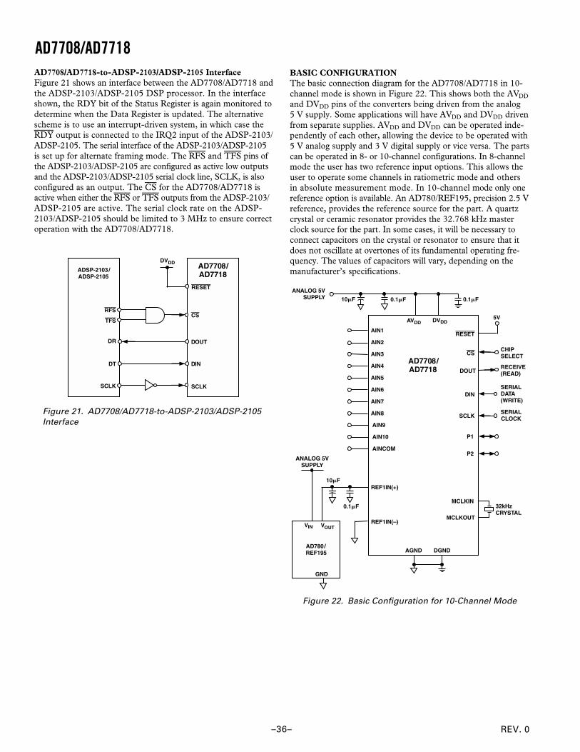
REV. 0–36–
AD7708/AD7718AD7708/AD7718-to-ADSP-2103/ADSP-2105 InterfaceFigure 21 shows an interface between the AD7708/AD7718 andthe ADSP-2103/ADSP-2105 DSP processor. In the interfaceshown, the RDY bit of the Status Register is again monitored todetermine when the Data Register is updated. The alternativescheme is to use an interrupt-driven system, in which case theRDY output is connected to the IRQ2 input of the ADSP-2103/ADSP-2105. The serial interface of the ADSP-2103/ADSP-2105is set up for alternate framing mode. The RFS and TFS pins ofthe ADSP-2103/ADSP-2105 are configured as active low outputsand the ADSP-2103/ADSP-2105 serial clock line, SCLK, is alsoconfigured as an output. The CS for the AD7708/AD7718 isactive when either the RFS or TFS outputs from the ADSP-2103/ADSP-2105 are active. The serial clock rate on the ADSP-2103/ADSP-2105 should be limited to 3 MHz to ensure correctoperation with the AD7708/AD7718.
DIN
RESET
DVDD
CS
AD7708/AD7718
SCLK
DOUT
SCLK
DT
DR
RFS
TFS
ADSP-2103/ADSP-2105
Figure 21. AD7708/AD7718-to-ADSP-2103/ADSP-2105Interface
BASIC CONFIGURATIONThe basic connection diagram for the AD7708/AD7718 in 10-channel mode is shown in Figure 22. This shows both the AVDD
and DVDD pins of the converters being driven from the analog5 V supply. Some applications will have AVDD and DVDD drivenfrom separate supplies. AVDD and DVDD can be operated inde-pendently of each other, allowing the device to be operated with5 V analog supply and 3 V digital supply or vice versa. The partscan be operated in 8- or 10-channel configurations. In 8-channelmode the user has two reference input options. This allows theuser to operate some channels in ratiometric mode and othersin absolute measurement mode. In 10-channel mode only onereference option is available. An AD780/REF195, precision 2.5 Vreference, provides the reference source for the part. A quartzcrystal or ceramic resonator provides the 32.768 kHz masterclock source for the part. In some cases, it will be necessary toconnect capacitors on the crystal or resonator to ensure that itdoes not oscillate at overtones of its fundamental operating fre-quency. The values of capacitors will vary, depending on themanufacturer’s specifications.
AD780/REF195
RECEIVE(READ)
P1
P2
AIN6
AIN5
AIN4
AIN3
AIN2
AIN1
0.1F
10F
ANALOG 5VSUPPLY
GND
VIN VOUT
AGND DGND
0.1F10F 0.1F
AVDD DVDD
REF1IN(+)
REF1IN(–)
RESET
CS
DOUT
DIN
SCLK
MCLKIN
MCLKOUT
5V
CHIPSELECT
SERIALDATA(WRITE)
SERIALCLOCK
32kHzCRYSTAL
ANALOG 5VSUPPLY
AD7708/AD7718
AIN8
AIN7
AIN9
AINCOM
AIN10
Figure 22. Basic Configuration for 10-Channel Mode

REV. 0
AD7708/AD7718
–37–
Analog Input ChannelsThe input multiplexer on AD7708/AD7718 can be configuredas either an 8- or 10-input channel device. This configuration isselected using the CHCON bit in the MODE register. WithCHCON = 0 (Figure 23), the user has eight input channels; thesecan be configured as eight pseudo-differential input channels withrespect to AINCOM or four fully-differential input channels.
In this configuration the user can select REFIN1 or REFIN 2 asthe reference for the selected channel using the REFSEL bit inthe mode register.
AIN6
AIN5
AIN4
AIN3
AIN2
AIN1AD7708/AD7718
AIN8
AIN7
REFIN1(+)
AINCOM
REFIN1(–)
REFIN2(+)
REFIN2(–)
AIN6
AIN5
AIN4
AIN3
AIN2
AIN1
AIN8
AIN7
REFIN1(+)
AINCOM
REFIN1(–)
REFIN2(+)
REFIN2(–)
Figure 23. Analog Input and Reference Options withCHCON = 0
With CHCON = 1 (Figure 24), the user has 10 input channelsthat can be configured as 10 pseudo-differential input channelswith respect to AINCOM or as five fully-differential input chan-nels. The contents of the CHCON bit overrides the REFSELbit. If the ADC is configured in five fully-differential or 10 pseudo-differential input channel mode, the REFSEL bit setting isirrelevant as only REFIN1 is available. Channel selection BitsCH3, CH2, CHI, and CH0 in the ADCCON register select theinput channel.
The input multiplexer switches the selected input channel to theon-chip buffer amplifier and sigma-delta converter. When theanalog input channel is switched, the settling time of the partmust elapse before a new valid word is available from the ADC.If any two inputs are configured as a differential input pair, thisinput is buffered and the common-mode and absolute input volt-age is restricted to a range between AGND + 100 mV and AVDD
– 100 mV. Care must be taken in setting up the common-modevoltage and input voltage range to ensure that these limits arenot exceeded, otherwise there will be a degradation in linearityand noise performance.
AIN6
AIN5
AIN4
AIN3
AIN2
AIN1AD7708/AD7718
AIN8
AIN7
REFIN1(+)
AINCOM
REFIN1(–)
AIN9
AIN10
AIN6
AIN5
AIN4
AIN3
AIN2
AIN1
AIN8
AIN7
REFIN1(+)
AINCOM
REFIN1(–)
AIN9
AIN10
Figure 24. Analog Input and Reference Options withCHCON = 1
Single-Ended OperationThe NEGBUF bit in the mode register is used to control theoperation of the input buffer on the AINCOM pin when config-ured for pseudo-differential mode of operation. If cleared, theanalog negative input (AINCOM) is unbuffered. It should benoted that the unbuffered input path on the AINCOM providesa dynamic load to the driving source. Therefore, resistor/capacitorcombinations on this input pin can cause dc gain errors depend-ing on the output impedance of the source that is driving theAINCOM input. AINCOM is tied to AGND for single-endedoperation. This enables all pseudo-differential inputs to act assingle-ended analog inputs. All analog inputs still operate inbuffered mode and their common-mode and absolute inputvoltage is restricted to a range between AGND + 100 mV andAVDD – 100 mV.
Chop Mode of Operation (CHOP = 0)The signal chain on the AD7708/AD7718 can be operated withchopping enabled or disabled. Chopping is enabled or disabledusing the CHOP bit in the mode register. The default mode ofoperation is for chop enabled (CHOP = 0). Optimum perfor-mance in terms of minimizing offset error and offset and gaindrift performance is achieved when chopping is enabled. Thedigital filter decimation rate, and consequently the output datarate, is programmable via the SF word loaded to the filter register.Output data rates vary from 5.35 Hz (186.77 ms) to 105.03 Hz
(9.52 ms). The output data rate f
fSF
ADCMOD=×24
.
The overall frequency response from the digital filter with chop-ping enabled is the product of a sinc3 and a sinc response. Thereare sinc3 notches at integer multiples of 3 × fADC and there aresinc notches at odd integer multiples of fADC/2. Normal moderejection is the major function of the digital filter on the AD7708/AD7718. The normal mode 50 ±1 Hz rejection with an SF wordof 82 is typically –100 dB. The 60 ± 1 Hz rejection with SF = 68 istypically –100 dB. Simultaneous 50 Hz and 60 Hz rejection ofbetter than 60 dB is achieved with an SF of 69 and gives a dataupdate rate of 19.8 Hz and a channel settling time of 101 ms. TheAD7708/AD7718 are factory-calibrated so field calibration willonly be required if the ADC is operated at temperatures that differsubstantially from the factory-calibration conditions.

REV. 0–38–
AD7708/AD7718Nonchop Mode of Operation (CHOP = 1)Chopping is enabled and disabled using the CHOP bit in themode register. Chopping is disabled by loading a 1 to the chopbit in the mode register. With chopping disabled the availableoutput rates vary from 16.06 Hz (62.26 ms) to 1365.33 Hz (0.73 ms).The range of applicable SF words is from 3 to 255. When thechopping is disabled the channel output data rate is increased by afactor of 3 compared to the situation when chopping is enabledand using the same SF word. When used in multiplexedapplications, operation with chop disabled will offer the bestthroughput time when cycling through all channels. The drawbackwith chop disabled is that the drift performance is degradedand calibration is required following a gain change or significanttemperature change. The output update and filter decimationrate is again controlled by the SF word loaded to the filterregister. The digital filter frequency response places sinc3
notches at integer multiples of the update rate. The output
update rate f
fSF
ADCMOD=×8
. The AD7708/AD7718 are targeted
at multiplexed applications and therefore operating with chopdisabled optimizes channel throughput time. One of the keyrequirements in these applications is the selection of an SF wordso as to obtain the maximum filter rejection at 50 Hz and 60 Hzwhile minimizing the channel throughput rate. This is achievedwith an SF word of 75 giving 57 dB rejection at 50 Hz, and60 dB rejection at 60 Hz while offering a channel throughputtime of 55 ms. Using a higher SF word of 151, 50 Hz and60 Hz rejection can be maximized at 60 dB with a channelthroughput rate of 110 ms. An SF word of 255 gives maximumrejection at both 50 Hz and 60 Hz but the channel throughputrate is restricted to 186 ms. Table XXI shows a quick comparisonof normal mode 50 Hz and 60 Hz rejection, settling time, andupdate rate for a selection of SF words with chop both enabledand disabled.
Programmable Gain AmplifierThe output from the buffer is applied to the input of the program-mable gain amplifier (PGA). The PGA gain range is programmedvia the range bits in the ADCCON register. The PGA has eightranges. With an external 2.5 V reference applied, and a PGAsetting of 128, the unipolar analog input range is 0 mV to 20 mV,while the bipolar analog input range is ±20 mV. With a PGAsetting of 1, the unipolar and bipolar input ranges are 2.56 V.When operating with chop mode enabled (CHOP = 0), the ADCrange-matching specification of 2 µV (typ) across all rangesmeans that calibration need only be carried out on a singlerange and does not have to be repeated when the PGA range ischanged. This is a significant advantage when compared withsimilar ADCs available on the market. Typical matching acrossranges is shown in Figure 25. Here, the ADC is configured infully-differential, bipolar mode with an external 2.5 V reference,while an analog input voltage of just greater than 19 mV is forcedon its analog inputs. The ADC continuously converts the dcvoltage at an update rate of 5.35 Hz, i.e., SF = FFhex, 800conversion results in total are gathered. The first 100 results aregathered with the ADC operating with a PGA setting of 128.
19.367
1000 200 400300
19.371
19.370
19.369
19.368
19.372
AD
C IN
PU
T V
OLT
AG
E –
mV
500
19.366
19.365
19.364600 700 800
SAMPLE COUNT
ADC RANGE
20
mV
40
mV
80
mV
16
0mV
32
0mV
64
0mV
1.
28V
2.
56V
Figure 25. ADC Range Matching
The PGA setting is then switched to 64 and 100 more resultsare gathered, and so on until the last 100 samples are gatheredwith a PGA setting of 1. From Figure 25, the variation in the samplemean through each range, i.e., the range matching, is seen to beof the order of 2 µV. When operating with chop mode disabled(CHOP = 1), new calibration data is needed (but not necessarilya new calibration) to remove offset error when switching channels.
Bipolar/Unipolar ConfigurationThe analog inputs on the AD7708/AD7718 can accept eitherunipolar or bipolar input voltage ranges. Bipolar input rangesdoes not imply that the part can handle negative voltages withrespect to system AGND. Signals in pseudo-differential modeare referenced to AINCOM, while in fully differential mode theyare referenced to the negative input of the differential input. Forexample, if AINCOM is 2.5 V and the AD7708/AD7718 AIN1analog input is configured for an analog input range of 0 mV to+20 mV, the input voltage range on the AIN1 input is 2.5 V to2.52 V. If AINCOM is 2.5 V and the AD7708/AD7718 is con-figured for an analog input range of ±1.28 V, the analog inputrange on the AIN1 input is 1.22 V to 3.78 V (i.e., 2.5 V ±1.28 V). Bipolar or unipolar options are chosen by programmingU/B bit in the ADCCON register. Programming for eitherunipolar or bipolar operation does not change any of the inputsignal conditioning; it simply changes the data output codingand the points on the transfer function where calibrations occur.
Data Output CodingWhen the AD7718 is configured for unipolar operation, the out-put coding is natural (straight) binary with a zero differentialinput voltage resulting in a code of 000 . . . 000, a midscalevoltage resulting in a code of 100 . . . 000, and a full-scale inputvoltage resulting in a code of 111 . . . 111. The output code forany analog input voltage can be represented as follows:
Code = (AIN × GAIN × 224)/(1.024 × VREF)
where
AIN is the analog input voltage,GAIN is the PGA gain, i.e., 1 on the 2.5 V range and 128 onthe 20 mV range.

REV. 0
AD7708/AD7718
–39–
The output code for any analog input voltage on the AD7708can be represented as follows:
Code = (AIN × GAIN × 216)/(1.024 × VREF)
where
AIN is the analog input voltage,GAIN is the PGA gain, i.e., 1 on the 2.5 V range and 128 onthe 20 mV range.
When an ADC is configured for bipolar operation, the coding isoffset binary with a negative full-scale voltage resulting in a codeof 000 . . . 000, a zero differential voltage resulting in a code of100 . . . 000, and a positive full-scale voltage resulting in a codeof 111 . . . 111. The output code from the AD7718 for anyanalog input voltage can be represented as follows:
Code = 223 × [(AIN × GAIN/(1.024 × VREF)) + 1]
where
AIN is the analog input voltage,GAIN is the PGA gain, i.e., 1 on the ±2.5 V range and 128 onthe ±20 mV range.
The output code from the AD7708 for any analog input voltagecan be represented as follows:
Code = 215 × [(AIN × GAIN/(1.024 × VREF)) + 1]
where
AIN is the analog input voltage,GAIN is the PGA gain, i.e., 1 on the ±2.5 V range and 128 onthe ±20 mV range.
Oscillator CircuitThe AD7708/AD7718 is intended for use with a 32.768 kHzwatch crystal or ceramic resonator. A PLL internally locks ontoa multiple of this frequency to provide a stable 4.194304 MHzclock for the ADC. The modulator sample rate is the same asthe oscillator frequency.
The start-up time associated with 32 kHz crystals is typically300 ms. The OSPD bit in the mode register can be used toprevent the oscillator from powering down when the AD7708/AD7718 is placed in power-down mode. This avoids having towait 300 ms after exiting power-down to start a conversion atthe expense of raising the power-down current.
Reference InputThe AD7708/AD7718 has a fully differential reference inputcapability. When the AD7708/AD7718 is configured in 8-channelmode (CHCON = 0) the user has the option of selecting one oftwo reference options. This allows the user to configure somechannels, for example, for ratiometric operation while others canbe configured for absolute value measurements. The REFSEL bitin the mode register allows selection of the required reference.If the REFSEL bit is cleared, the reference selected is REFIN1(+)–REFIN1(–) for the active channel. If this bit is set, the refer-ence selected is REFIN2(+) – REFIN2(–) for the active channel.When the AD7708/AD7718 is configured in 10-channel mode(CHCON = 1) the user has only one reference option (REFIN1).The contents of the CHCON bit overrides the REFSEL bit. If
the ADC is configured in five fully-differential or 10 pseudo-differential input channel mode, the REFSEL bit setting isirrelevant as only one reference input is available.
The common-mode range for these differential inputs is fromAGND to AVDD. The reference inputs are unbuffered andtherefore excessive R-C source impedances will introduce gainerrors. The nominal reference voltage for specified operation,VREF, (REFIN1(+)–REFIN1(–) or REFIN2(+)–REFIN2(–)),is 2.5 V, but the AD7708/AD7718 is functional with referencevoltages from 1 V to AVDD. In applications where the excitation(voltage or current) for the transducer on the analog input alsodrives the reference voltage for the part, the effect of the lowfrequency noise in the excitation source will be removed as theapplication is ratiometric. If the AD7708/AD7718 is used in anonratiometric application, a low noise reference should beused. Recommended reference voltage sources for the AD7708/AD7718 include the AD780, REF43, and REF192. It shouldalso be noted that the reference inputs provide a high impedance,dynamic load. Because the input impedance of each referenceinput is dynamic, resistor/capacitor combinations on these inputscan cause dc gain errors, depending on the output impedance ofthe source that is driving the reference inputs. Reference voltagesources, like those recommended above (e.g., AD780) will typicallyhave low output impedances and are therefore tolerant of havingdecoupling capacitors on the REFIN(+) without introducing gainerrors in the system. Deriving the reference input voltage acrossan external resistor will mean that the reference input sees asignificant external source impedance. External decoupling onthe REFIN(+) and REFIN(–) pins would not be recommendedin this type configuration.
RESET InputThe RESET input on the AD7708/AD7718 resets all the logic,the digital filter and the analog modulator while all on-chipregisters are reset to their default state. RDY is driven high andthe AD7708/AD7718 ignores all communications to any of itsregisters while the RESET input is low. When the RESET inputreturns high the AD7708/AD7718 operates with its default setupconditions and it is necessary to set up all registers and carry outa system calibration if required after a RESET command.
Power-Down ModeLoading 0, 0, 0 to the MD2, MD1, MD0 bits in the ADC moderegister places the ADC in device power-down mode. Devicepower-down mode is the default condition for the AD7708/AD7718 on power-up. The ADC retains the contents of all itson-chip registers (including the data register) while in power-down. The device power-down mode does not affect the digitalinterface, but does affect the status of the RDY pin. Writing theAD7708/AD7718 into power-down will reset the RDY line high.Placing the part in power-down mode reduces the total current(AIDD + DIDD) to 31 µA max when the part is operated at 5 Vand the oscillator allowed to run during power-down mode.With the oscillator shut down the total IDD is typically 9 µA.

REV. 0–40–
AD7708/AD7718CalibrationThe AD7708/AD7718 provides four calibration modes that canbe programmed via the mode bits in the mode register. One ofthe major benefits of the AD7708/AD7718 is that it is factory-calibrated with chopping enabled as part of the final test processwith the generated coefficients stored within the ADC. At power-on, the factory gain calibration coefficients are automaticallyloaded to the gain calibration registers on the AD7708/AD7718.This gives excellent offset and drift performance and it isenvisaged that in the majority of applications the user will notneed to perform any field calibrations. Also, because factorygain calibration coefficients (generated at 25°C ambient) areautomatically present at power-on, an internal full-scale calibrationwill only be required if the part is being operated at temperaturessignificantly different from 25°C.
When chopping is disabled (CHOP =1) the AD7708/AD7718requires an offset calibration or new calibration coefficients onrange changing or when significant temperature changes occuras the signal chain is no longer chopped and offset and drifterrors are no longer removed as part of the conversion process.
The factory-calibration values for any one channel will be over-written if any one of the four calibration options is initiated.The AD7708/AD7718 offers “internal” or “system” calibrationfacilities. For full calibration to occur, the calibration logic mustrecord the modulator output for two different input conditions.These are “zero-scale” and “full-scale” points. These pointsare derived by performing a conversion on the different inputvoltages provided to the input of the modulator during calibration.The result of the “zero-scale” calibration conversion is stored inthe Offset Calibration Registers for the appropriate channel.The result of the “full-scale” calibration conversion is storedin the Gain Calibration Registers. With these readings, thecalibration logic can calculate the offset and the gain slope forthe input-to-output transfer function of the converter. During an“internal” zero-scale or full-scale calibration, the respective“zero” input and “full-scale” input are automatically connectedto the ADC input pins internally to the device. A “system” cali-bration, however, expects the system zero-scale and systemfull-scale voltages to be applied to the external ADC pinsbefore the calibration mode is initiated. In this way externalADC errors are taken into account and minimized as a resultof system calibration. It should also be noted that to optimizecalibration accuracy, all AD7708/AD7718 ADC calibrationsare carried out automatically at the slowest update rate withchop enabled. When chop mode is disabled calibrations arecarried out at the update rate defined by the SF word in thefilter register.
Internally in the AD7708/AD7718, the coefficients are normalizedbefore being used to scale the words coming out of the digitalfilter. The offset calibration coefficient is subtracted from theresult prior to the multiplication by the gain coefficient. Withchopping disabled AD7708/AD7718 ADC specifications willonly apply after a zero-scale calibration at the operating point ofinterest. From an operational point of view, a calibration shouldbe treated like another ADC conversion. A zero-scale calibration(if required) should always be carried out before a full-scale
calibration. System software should monitor the RDY bit in theSTATUS register to determine end of calibration via a pollingsequence or interrupt driven routine.
Grounding and LayoutSince the analog inputs and reference inputs are differential,most of the voltages in the analog modulator are common-modevoltages. The excellent common-mode rejection of the part willremove common-mode noise on these inputs. The analog anddigital supplies to the AD7708/AD7718 are independent andseparately pinned out to minimize coupling between the analogand digital sections of the device. The AD7708/AD7718 can beoperated with 5 V analog and 3 V digital supplies or vice versa.The digital filter will provide rejection of broadband noise onthe power supplies, except at integer multiples of the modulatorsampling frequency. The digital filter also removes noise fromthe analog and reference inputs provided these noise sources donot saturate the analog modulator. As a result, the AD7708/AD7718 is more immune to noise interference than a conventionalhigh-resolution converter. However, because the resolution of theAD7708/AD7718 is so high and the noise levels from theconverter so low, care must be taken with regard to groundingand layout.
The printed circuit board that houses the ADC should be designedso the analog and digital sections are separated and confined tocertain areas of the board. This facilitates the use of ground planesthat can be easily separated. A minimum etch technique isgenerally best for ground planes as it gives the best shielding.
Although the AD7708/AD7718 has separate pins for analog anddigital ground, the AGND and DGND pins are tied togetherinternally via the substrate. Therefore, the user must not tiethese two pins to separate ground planes unless the groundplanes are connected together near the AD7708/AD7718.
In systems where the AGND and DGND are connected some-where else in the system, i.e., the systems power supply, theyshould not be connected again at the AD7708/AD7718 or aground loop will result. In these situations it is recommended thatground pins of the AD7708/AD7718 be tied to the AGND plane.
In any layout it is implicit that the user keep in mind the flow ofcurrents in the system, ensuring that the paths for all currentsare as close as possible to the paths the currents took to reachtheir destinations. Avoid forcing digital currents to flow throughthe AGND.
Avoid running digital lines under the device as these will couplenoise onto the die. The analog ground plane should be allowedto run under the AD7708/AD7718 to prevent noise coupling.The power supply lines to the AD7708/AD7718 should use aswide a trace as possible to provide low impedance paths andreduce the effects of glitches on the power supply line. Fastswitching signals like clocks should be shielded with digitalground to avoid radiating noise to other sections of the boardand clock signals should never be run near the analog inputs.Avoid crossover of digital and analog signals. Traces on oppositesides of the board should run at right angles to each other. This willreduce the effects of feedthrough through the board. A microstriptechnique is by far the best, but is not always possible with adouble-sided board. In this technique, the component side ofthe board is dedicated to ground planes while signals are placedon the solder side.
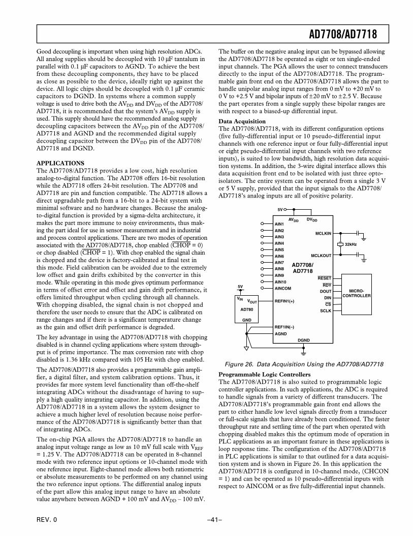
REV. 0
AD7708/AD7718
–41–
Good decoupling is important when using high resolution ADCs.All analog supplies should be decoupled with 10 µF tantalum inparallel with 0.1 µF capacitors to AGND. To achieve the bestfrom these decoupling components, they have to be placedas close as possible to the device, ideally right up against thedevice. All logic chips should be decoupled with 0.1 µF ceramiccapacitors to DGND. In systems where a common supplyvoltage is used to drive both the AVDD and DVDD of the AD7708/AD7718, it is recommended that the system’s AVDD supply isused. This supply should have the recommended analog supplydecoupling capacitors between the AVDD pin of the AD7708/AD7718 and AGND and the recommended digital supplydecoupling capacitor between the DVDD pin of the AD7708/AD7718 and DGND.
APPLICATIONSThe AD7708/AD7718 provides a low cost, high resolutionanalog-to-digital function. The AD7708 offers 16-bit resolutionwhile the AD7718 offers 24-bit resolution. The AD7708 andAD7718 are pin and function compatible. The AD7718 allows adirect upgradable path from a 16-bit to a 24-bit system withminimal software and no hardware changes. Because the analog-to-digital function is provided by a sigma-delta architecture, itmakes the part more immune to noisy environments, thus mak-ing the part ideal for use in sensor measurement and in industrialand process control applications. There are two modes of operationassociated with the AD7708/AD7718, chop enabled (CHOP = 0)or chop disabled (CHOP = 1). With chop enabled the signal chainis chopped and the device is factory-calibrated at final test inthis mode. Field calibration can be avoided due to the extremelylow offset and gain drifts exhibited by the converter in thismode. While operating in this mode gives optimum performancein terms of offset error and offset and gain drift performance, itoffers limited throughput when cycling through all channels.With chopping disabled, the signal chain is not chopped andtherefore the user needs to ensure that the ADC is calibrated onrange changes and if there is a significant temperature changeas the gain and offset drift performance is degraded.
The key advantage in using the AD7708/AD7718 with choppingdisabled is in channel cycling applications where system through-put is of prime importance. The max conversion rate with chopdisabled is 1.36 kHz compared with 105 Hz with chop enabled.
The AD7708/AD7718 also provides a programmable gain ampli-fier, a digital filter, and system calibration options. Thus, itprovides far more system level functionality than off-the-shelfintegrating ADCs without the disadvantage of having to sup-ply a high quality integrating capacitor. In addition, using theAD7708/AD7718 in a system allows the system designer toachieve a much higher level of resolution because noise perfor-mance of the AD7708/AD7718 is significantly better than thatof integrating ADCs.
The on-chip PGA allows the AD7708/AD7718 to handle ananalog input voltage range as low as 10 mV full scale with VREF
= 1.25 V. The AD7708/AD7718 can be operated in 8-channelmode with two reference input options or 10-channel mode withone reference input. Eight-channel mode allows both ratiometricor absolute measurements to be performed on any channel usingthe two reference input options. The differential analog inputsof the part allow this analog input range to have an absolutevalue anywhere between AGND + 100 mV and AVDD – 100 mV.
The buffer on the negative analog input can be bypassed allowingthe AD7708/AD7718 be operated as eight or ten single-endedinput channels. The PGA allows the user to connect transducersdirectly to the input of the AD7708/AD7718. The program-mable gain front end on the AD7708/AD7718 allows the part tohandle unipolar analog input ranges from 0 mV to +20 mV to0 V to +2.5 V and bipolar inputs of ±20 mV to ±2.5 V. Becausethe part operates from a single supply these bipolar ranges arewith respect to a biased-up differential input.
Data AcquisitionThe AD7708/AD7718, with its different configuration options(five fully-differential input or 10 pseudo-differential inputchannels with one reference input or four fully-differential inputor eight pseudo-differential input channels with two referenceinputs), is suited to low bandwidth, high resolution data acquisi-tion systems. In addition, the 3-wire digital interface allows thisdata acquisition front end to be isolated with just three opto-isolators. The entire system can be operated from a single 3 Vor 5 V supply, provided that the input signals to the AD7708/AD7718’s analog inputs are all of positive polarity.
5V
AD780
AIN6
AIN5
AIN4
AIN3
AIN2
AIN1
5V
GND
VIN VOUT
AGND
DGND
AVDD DVDD
REF1IN(–)
MCLKIN
MCLKOUT
32kHz
AD7708/AD7718AIN8
AIN7
AIN9
AINCOM
AIN10
MICRO-CONTROLLER
SCLK
CS
DIN
DOUT
RDY
RESET
REFIN1(+)
Figure 26. Data Acquisition Using the AD7708/AD7718
Programmable Logic ControllersThe AD7708/AD7718 is also suited to programmable logiccontroller applications. In such applications, the ADC is requiredto handle signals from a variety of different transducers. TheAD7708/AD7718’s programmable gain front end allows thepart to either handle low level signals directly from a transduceror full-scale signals that have already been conditioned. The fasterthroughput rate and settling time of the part when operated withchopping disabled makes this the optimum mode of operation inPLC applications as an important feature in these applications isloop response time. The configuration of the AD7708/AD7718in PLC applications is similar to that outlined for a data acquisi-tion system and is shown in Figure 26. In this application theAD7708/AD7718 is configured in 10-channel mode, (CHCON= 1) and can be operated as 10 pseudo-differential inputs withrespect to AINCOM or as five fully-differential input channels.

REV. 0–42–
AD7708/AD7718Converting Single-Ended InputsThe AD7708/AD7718 generally operates in buffered mode. Thisplaces a restriction of AGND + 100 mV to AVDD – 100 mV onthe absolute and common-mode voltages that can be applied toany input on the AD7708/AD7718.
Some applications may require the measurement of analoginputs with respect to AGND. To enable the AD7708/AD7718to be used in these single-ended applications, the buffer on theAINCOM can be bypassed. The NEGBUF bit in the moderegister controls the operation of the input buffer on the AINCOMinput when a channel is configured for pseudo-differential mode ofoperation. If cleared, the analog negative input (AINCOM) isunbuffered, allowing it to be tied to AGND in single-endedinput configuration. If this bit is set, the analog negative input(AINCOM) is buffered, placing a restriction on its common-mode input range. When AINCOM is unbuffered, signals with acommon-mode range from AGND – 30 mV to AVDD + 30 mVcan be accommodated on this input allowing the end user toconnect the AINCOM input to AGND and perform single-ended measurements with respect to this input. This unbufferedinput path on the AINCOM provides a dynamic load to thedriving source. Therefore, resistor/capacitor combinations onthis input pin can cause dc gain errors, depending on the outputimpedance of the source that is driving the AINCOM input. Allanalog inputs still operate in buffered mode and their com-mon-mode and absolute input voltage is restricted to a rangebetween AGND + 100 mV and AVDD – 100 mV.
Combined Ratiometric and Absolute Value MeasurementSystemThe AD7708/AD7718 when operated with CHCON = 0 can beconfigured for operation as four fully-differential analog inputs oreight pseudo-differential analog inputs with two fully-differentialreference inputs. Having the ability to use either REFIN1 orREFIN2 with any channel during the conversion process allowsthe end user to make both absolute and ratiometric measure-ments as shown in Figure 27. In this example a fully-differentialanalog input (AIN1–AIN2) is being converted from a bridge trans-ducer in a ratiometric manner using REFIN1 as the referenceinput for this channel. AIN3 is configured as a pseudo-differentialinput channel using REFIN2 to perform an absolute measurementon the potentiometer. The REFSEL bit in the mode register isused to select which reference is used with the active channelduring the conversion process. When the AD7708/AD7718 isconfigured with CHCON = 1, only one reference (REFIN1) isavailable. The contents of the CHCON bit override the REFSELbit. If the ADC is configured in five fully-differential or 10pseudo-differential input channel mode, the REFSEL bit settingis irrelevant as only REFIN1 is available.
REFIN1(–)
AD7718
REFIN2(+)
REFIN1(+)
AINCOM
AIN1
AIN3
AIN2
REFIN2(–)GND
EXCITATION VOLTAGE = 4V
WIPER
Figure 27. Absolute and Ratiometric MeasurementSystem Using AD7718

REV. 0
AD7708/AD7718
–43–
Table XXI. Normal Mode 50 Hz and 60 Hz Rejection vs. Settling Time and Update Rate for a Selection of SF Words
CHOP Disabled CHOP Enabled
50 Hz 1 Hz 60 Hz 1 Hz 50 Hz 1 Hz 60 Hz 1 HzSF Rejection Rejection Rejection RejectionWord fADC (Hz) tSETTLE (ms) (dB) (dB) fADC (Hz) tSETTLE (ms) (dB) (dB)
03 1365.33 2.20 0.05 0.08 N/A N/A N/A N/A13 315.08 9.52 1 1.5 105.03 19.04 21 13.669 59.36 50.54 42 94 19.79 101 60 9475 54.6 54.93 57 60 18.2 110 62 6682 49.95 60 100 16.65 180 100 53151 27.13 110.6 60 60 9.04 221 72 63255 16.06 186.76 77 68 5.35 373.5 93 68
Optimizing Throughput while Maximizing 50 Hz and 60 HzRejection in a Multiplexed Data Acquisition SystemThe AD7708/AD7718 can be optimized for one of two modesof operation. Operating the AD7708/AD7718 with choppingenabled (CHOP = 0) optimizes the AD7708/AD7718 for analogperformance over channel throughput. Output data rates varyfrom 5.35 Hz (186.77 ms) to 105.03 Hz (9.52 ms). Optimumperformance, in terms of minimizing offset error and offset andgain drift performance, is achieved as a result of chopping thesignal chain.
With chopping disabled the available output rates vary from16.06 Hz (62.26 ms) to 1365.33 Hz (0.73 ms). The range ofapplicable SF words is from 3 to 255. When the chopping isdisabled the channel output data rate is increased by a factor of3 compared to the situation when chopping is enabled isdisabled. When used in multiplexed applications, operationwith chop disabled will offer the best throughput time when
cycling through all channels. The drawback with choppingdisabled is that the drift performance is degraded and calibra-tion is required following gain and temperature changes. Oneof the key requirements in these applications is to optimize the SFword to obtain the maximum filter rejection at 50 Hz and 60 Hzwhile minimizing the channel throughput rate. This is achievedwith an SF word of 75 giving 57 dB rejection at 50 Hz and60 dB rejection at 60 Hz while offering a channel throughputtime of 55 ms.
Using a higher SF word of 151, 50 Hz and 60 Hz rejection canbe maximized at 60 dB with a channel throughput rate of 110 ms.An SF word of 255 gives maximum rejection at both 50 Hzand 60 Hz, but the channel throughput rate is restricted to186 ms. Table XXI gives a quick comparison of normal mode 50 Hzand 60 Hz rejection, settling time, and update rate for a selec-tion of SF words with both chopping enabled and disabled.

REV. 0–44–
C01
831–
1–7/
01(0
)P
RIN
TE
D IN
U.S
.A.
AD7708/AD7718
28-Lead Plastic SOIC(R-28)
0.0125 (0.32)0.0091 (0.23)
80
0.0291 (0.74)0.0098 (0.25)
45
0.0500 (1.27)0.0157 (0.40)
SEATINGPLANE
0.0118 (0.30)0.0040 (0.10)
0.0192 (0.49)0.0138 (0.35)
0.1043 (2.65)0.0926 (2.35)
0.0500(1.27)BSC
28 15
141
0.7125 (18.10)0.6969 (17.70)
0.4193 (10.65)0.3937 (10.00)
0.2992 (7.60)0.2914 (7.40)
PIN 1
28-Lead Plastic TSSOP(RU-28)
0.177 (4.50)0.169 (4.30)
28 15
141
0.386 (9.80)0.378 (9.60)
0.256 (6.50)0.246 (6.25)
PIN 1
SEATINGPLANE
0.006 (0.15)0.002 (0.05)
0.0118 (0.30)0.0075 (0.19)
0.0256 (0.65)BSC
0.0433 (1.10)MAX
0.0079 (0.20)0.0035 (0.090)
0.028 (0.70)0.020 (0.50)
80
OUTLINE DIMENSIONSDimensions shown in inches and (mm).