Embed Size (px)
Citation preview

16-Bit, 4-Channel/8-Channel, 250 kSPS PulSAR ADCs
Data Sheet AD7682/AD7689
Rev. J Document Feedback Information furnished by Analog Devices is believed to be accurate and reliable. However, no responsibility is assumed by Analog Devices for its use, nor for any infringements of patents or other rights of third parties that may result from its use. Specifications subject to change without notice. No license is granted by implication or otherwise under any patent or patent rights of Analog Devices. Trademarks and registered trademarks are the property of their respective owners.
One Technology Way, P.O. Box 9106, Norwood, MA 02062-9106, U.S.A. Tel: 781.329.4700 ©2008–2019 Analog Devices, Inc. All rights reserved. Technical Support www.analog.com
FEATURES 16-bit resolution with no missing codes 4-channel (AD7682)/8-channel (AD7689) multiplexer with
choice of inputs Unipolar single-ended Differential (GND sense) Pseudobipolar Throughput: 250 kSPS INL: ±0.4 LSB typical, ±1.5 LSB maximum (±23 ppm or FSR) Dynamic range: 93.8 dB SINAD: 92.5 dB at 20 kHz THD: −100 dB at 20 kHz Analog input range: 0 V to VREF with VREF up to VDD Multiple reference types
Internal selectable 2.5 V or 4.096 V External buffered (up to 4.096 V) External (up to VDD)
Internal temperature sensor (TEMP) Channel sequencer, selectable 1-pole filter, busy indicator No pipeline delay, SAR architecture Single-supply 2.3 V to 5.5 V operation with 1.8 V to 5.5 V
logic interface Serial interface compatible with SPI, MICROWIRE, QSPI,
and DSP Power dissipation
3.5 mW at 2.5 V/200 kSPS 12.5 mW at 5 V/250 kSPS
Standby current: 50 nA Low cost grade available 20-lead 4 mm × 4 mm LFCSP package 20-lead 2.4 mm × 2.4 mm WLCSP package
APPLICATIONS Multichannel system monitoring Battery-powered equipment Medical instruments: ECG/EKG Mobile communications: GPS Power line monitoring Data acquisition Seismic data acquisition systems Instrumentation Process control
FUNCTIONAL BLOCK DIAGRAM
AD7682/AD7689
REF
GND
VDD
VIO
DIN
SCK
SDO
CNV
1.8VTOVDD
2.3V TO 5.5V
SEQUENCER
SPI SERIALINTERFACE
MUX 16-BIT SARADC
BAND GAPREF
TEMPSENSOR
REFIN
IN0IN1
IN4IN5IN6IN7
IN3IN2
COM
0.5V TO VDD10µF
ONE-POLELPF
0.5V TO VDD – 0.5V0.1µF
0735
3-00
1
Figure 1.
GENERAL DESCRIPTION The AD7682/AD7689 are 4-channel/8-channel, 16-bit, charge redistribution successive approximation register (SAR) analog-to-digital converters (ADCs) that operate from a single power supply, VDD.
The AD7682/AD7689 contain all components for use in a multichannel, low power data acquisition system, including a true 16-bit SAR ADC with no missing codes; a 4-channel (AD7682) or 8-channel (AD7689) low crosstalk multiplexer that is useful for configuring the inputs as single-ended (with or without ground sense), differential, or bipolar; an internal low drift reference (selectable 2.5 V or 4.096 V) and buffer; a temperature sensor; a selectable one-pole filter; and a sequencer that is useful when channels are continuously scanned in order.
The AD7682/AD7689 use a simple serial port interface (SPI) for writing to the configuration register and receiving conversion results. The SPI interface uses a separate supply, VIO, which is set to the host logic level. Power dissipation scales with throughput.
Continued on Page 4

AD7682/AD7689 Data Sheet
Rev. J | Page 2 of 38
TABLE OF CONTENTS Features .............................................................................................. 1 Applications ....................................................................................... 1 Functional Block Diagram .............................................................. 1 General Description ......................................................................... 1 Revision History ............................................................................... 2 Specifications ..................................................................................... 5
Timing Specifications .................................................................. 9 Absolute Maximum Ratings .......................................................... 12
ESD Caution ................................................................................ 12 Pin Configurations and Function Descriptions ......................... 13 Typical Performance Characteristics ........................................... 17 Terminology .................................................................................... 20 Theory of Operation ...................................................................... 21
Overview ...................................................................................... 21 Converter Operation .................................................................. 21 Transfer Functions...................................................................... 22 Typical Connection Diagrams .................................................. 23 Analog Inputs .............................................................................. 24 Driver Amplifier Choice ............................................................ 26
Voltage Reference Output/Input .............................................. 26 Power Supply ............................................................................... 28 Supplying the ADC from the Reference .................................. 28
Digital Interface .............................................................................. 29 Reading/Writing During Conversion, Fast Hosts .................. 29 Reading/Writing After Conversion, Any Speed Hosts .......... 29 Reading/Writing Spanning Conversion, Any Speed Host .... 29 Configuration Register, CFG .................................................... 29 General Timing Without a Busy Indicator ............................. 31 General Timing with a Busy Indicator .................................... 32 Channel Sequencer .................................................................... 33 Read/Write Spanning Conversion Without a Busy Indicator ...................................................................................... 34 Read/Write Spanning Conversion with a Busy Indicator ..... 35
Applications Information .............................................................. 36 Layout .......................................................................................... 36 Evaluating the AD7682/AD7689 Performance ........................ 36
Outline Dimensions ....................................................................... 37 Ordering Guide .......................................................................... 38
REVISION HISTORY 11/2019—Rev. I to Rev. J Updated Outline Dimensions ....................................................... 37 11/2019—Rev. H to Rev. I Changes to General Description Section ...................................... 4 Changes to Table 2 ............................................................................ 5 Added Table 3; Renumbered Sequentially .................................... 7 Changes to Table 4 ............................................................................ 8 Changes to Timing Specifications Section .................................... 9 Changes to Table 6 .......................................................................... 10 Changes to Pin 1, Pin 20 Description, Table 8 ............................ 13 Changes to Pin B6, Pin B8 Description, Table 9......................... 15 Changes to Figure 38 ...................................................................... 28 Updated Outline Dimensions ....................................................... 37 Changes to Ordering Guide .......................................................... 38 8/2017—Rev. G to Rev. H Changed CP-20-8 to CP-20-10 .................................... Throughout Change to Product Title ................................................................... 1 Updated Outline Dimensions ....................................................... 34 Changes to Ordering Guide .......................................................... 35 6/2017—Rev. F to Rev. G Changed CP-20-10 to CP-20-8 .................................... Throughout Changes to Table 11 ........................................................................ 27 Updated Outline Dimensions ....................................................... 34
Changes to Ordering Guide .......................................................... 35 4/2016—Rev. E to Rev. F Changed ADA4841-x to ADA4805-1/ADA4807-1, Table 1 ........ 1 Added Endnote 6, Table 3; Renumbered Sequentially ................. 6 Changes to Figure 28 and Figure 29 ............................................ 20 Changes to Table 10 ....................................................................... 23 Changes to External Reference Section and the Reference Decoupling Section ........................................................................ 24 Changes to the Supplying the ADC from the Reference Section .. 25 Changes to Ordering Guide .......................................................... 35 1/2015—Rev. D to Rev. E Added WLCSP (Throughout) ......................................................... 1 Added WLCSP Signal-to-Noise and SINAD Parameters; Table 2 ................................................................................................. 3 Changed θJA Thermal Impedance (LFCSP) from 47.6°C/W to 48°C/W ............................................................................................... 9 Added Figure 6, Figure 7, and Table 8 ......................................... 12 Changes to Layout Section ............................................................ 33 Added Figure 47; Outline Dimensions ........................................ 34 Changes to Ordering Guide .......................................................... 35
Data Sheet AD7682/AD7689
Rev. J | Page 3 of 38
4/2012—Rev. C to Rev. D Changes to Figure 27 ...................................................................... 18 Changed Internal Reference Section to Internal Reference/Temperature Sensor Section ....................................... 21 Changes to Internal Reference/Temperature Sensor Section .... 21 Changed External Reference/Temperature Sensor Section to External Reference Section ............................................................ 22 Changes to External Reference and Internal Buffer Section and External Reference Section ............................................................ 22 Changes to REF Bit, Function Column, Table 10 ....................... 25 Updated Outline Dimensions ........................................................ 32 9/2011—Rev. B to Rev. C Changes to Internal Reference Section ........................................ 21 Changes to the External Reference and Internal Buffer Section .............................................................................................. 22 Changes to the External Reference/Temperature Sensor Section .............................................................................................. 22 Changes to Table 10, REF Bit Description ................................... 25 6/2009—Rev. A to Rev. B Changes Table 6 ................................................................................. 8 Changes to Figure 37 ...................................................................... 25 Changes to Figure 38 ...................................................................... 26 3/2009—Rev. 0 to Rev. A Changes to Features Section, Applications Section, and Figure 1 ............................................................................................... 1 Added Table 2; Renumbered Sequentially ..................................... 3 Changed VREF to VREF ..................................................................... 4 Changes to Table 3 ............................................................................ 5 Changes to Table 4 ............................................................................ 6 Changes to Table 5 ............................................................................ 7 Deleted Endnote 2 in Table 6 ........................................................... 8
Changes to Figure 4, Figure 5, and Table 7 .................................... 9 Changes to Figure 6, Figure 9, and Figure 10 .............................. 11 Changes to Figure 22 ...................................................................... 13 Changes to Overview Section and Converter Operation Section .............................................................................................. 15 Changes to Table 8 .......................................................................... 16 Changes to Figure 26 and Figure 27 ............................................. 17 Changes to Bipolar Single Supply Section and Analog Inputs Section .............................................................................................. 18 Changes to Internal Reference/Temperature Sensor Section .... 20 Added Figure 31; Renumbered Sequentially ............................... 20 Changes to External Reference and Internal Buffer Section and External Reference Section ............................................................ 21 Added Figure 32 and Figure 33 ..................................................... 21 Changes to Power Supply Section ................................................. 22 Changes to Digital Interface Section, Reading/Writing After Conversion, Any Speed Hosts Section, and Configuration Register, CFG Section ..................................................................... 23 Changes to Table 10 ........................................................................ 24 Added General Timing Without a Busy Indicator Section and Figure 37 ........................................................................................... 25 Added General Timing With a Busy Indicator Section and Figure 38 ........................................................................................... 26 Added Channel Sequencer Section and Figure 39 ..................... 27 Changes to Read/Write Spanning Conversion Without a Busy Indicator Section and Figure 41 .................................................... 28 Changes to Read/Write Spanning Conversion with a Busy Indicator and Figure 43 .................................................................. 29 Changes to Evaluating AD7682/AD7689 Performance Section .............................................................................................. 30 Added Exposed Pad Notation to Outline Dimensions .............. 31 Changes to Ordering Guide ........................................................... 31 5/2008—Revision 0: Initial Version
AD7682/AD7689 Data Sheet
Rev. J | Page 4 of 38
The AD7682/AD7689 are housed in a tiny 20-lead lead frame chip scale package (LFCSP) and 20-lead wafer level chip scale package (WLCSP) with operation specified from −40°C to +85°C. The AD7689 includes an extended temperature range model with specifications guaranteed to a maximum temperature (TMAX) of +125°C.
Table 1. Multichannel 14-Bit/16-Bit PulSAR® ADCs Type Channels 250 kSPS 500 kSPS ADC Driver 14-Bit 8 AD7949 ADA4805-1/
ADA4807-1 16-Bit 4 AD7682 ADA4805-1/
ADA4807-1 16-Bit 8 AD7689 AD7699 ADA4805-1/
ADA4807-1

Data Sheet AD7682/AD7689
Rev. J | Page 5 of 38
SPECIFICATIONS VDD = 2.3 V to 5.5 V, VIO = 1.8 V to VDD, reference voltage (VREF) = VDD, all specifications, TA = −40°C to +85°C, unless otherwise noted.
Table 2.
Parameter Test Conditions/ Comments
AD7689A AD7682B/AD7689B Unit Min Typ Max Min Typ Max
RESOLUTION 16 16 Bits ANALOG INPUT
Voltage Range Unipolar mode 0 +VREF 0 +VREF V Bipolar mode −VREF/2 +VREF/2 −VREF/2 +VREF/2 V Absolute Input Voltage Positive input, unipolar
and bipolar modes −0.1 VREF + 0.1 −0.1 VREF + 0.1 V
Negative or COM input, unipolar mode
−0.1 +0.1 −0.1 +0.1 V
Negative or COM input, bipolar mode
VREF/2 − 0.1 VREF/2 VREF/2 + 0.1 VREF/2 − 0.1 VREF/2 VREF/2 + 0.1 V
Analog Input CMRR1 Input frequency (fIN) = 250 kHz
68 68 dB
Leakage Current at 25°C Acquisition phase 1 1 nA Input Impedance2
THROUGHPUT Conversion Rate
Full Bandwidth3 VDD = 4.5 V to 5.5 V 0 250 0 250 kSPS VDD = 2.3 V to 4.5 V 0 200 0 200 kSPS ¼ Bandwidth3 VDD = 4.5 V to 5.5 V 0 62.5 0 62.5 kSPS
VDD = 2.3 V to 4.5 V 0 50 0 50 kSPS Transient Response Full-scale step, full
bandwidth 1.8 1.8 µs
Full-scale step, ¼ bandwidth
14.5 14.5 µs
ACCURACY No Missing Codes 15 16 Bits Integral Linearity Error −4 +4 −1.5 ±0.4 +1.5 LSB4 Differential Linearity Error −1 ±0.25 +1.5 LSB Transition Noise REF = VDD = 5 V 0.6 0.5 LSB Gain Error5 −32 +32 −8 ±1 +8 LSB Gain Error Match ±2 −4 ±0.5 +4 LSB Gain Error Temperature
Drift ±1 ±1 ppm/°C
Offset Error5 VDD = 4.5 V to 5.5 V −32 +32 −8 ±1 +8 LSB VDD = 2.3 V to 4.5 V ±32 ±5 LSB Offset Error Match ±2 −4 ±0.5 +4 LSB Offset Error Temperature
Drift ±1 ±1 ppm/°C
Power Supply Sensitivity VDD = 5 V ± 5% ±1.5 ±1.5 LSB AC ACCURACY6
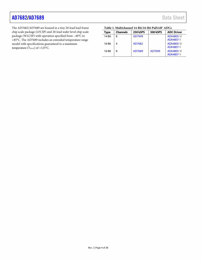
Dynamic Range 90.5 93.8 dB7 Signal-to-Noise (SNR)
LFCSP fIN = 20 kHz, VREF = 5 V 90 92.5 93.5 dB fIN = 20 kHz, VREF =
4.096 V, internal REF 89 91 92.3 dB
fIN = 20 kHz, VREF = 2.5 V, internal REF
86 87.5 88.8 dB
AD7682/AD7689 Data Sheet
Rev. J | Page 6 of 38
Parameter Test Conditions/ Comments
AD7689A AD7682B/AD7689B Unit Min Typ Max Min Typ Max
WLFCSP fIN = 20 kHz, VREF = 5 V 91 92 dB fIN = 20 kHz, VREF =
4.096 V, internal REF 89.5 91 dB
fIN = 20 kHz, VREF = 2.5 V, internal REF
86 87.5 dB
SINAD8 LFCSP fIN = 20 kHz, VREF = 5 V 89 91 92.5 dB
fIN = 20 kHz, VREF = 5 V, −60 dB input
30.5 33.5 dB
fIN = 20 kHz, VREF = 4.096 V, internal REF
88 90 91 dB
fIN = 20 kHz, VREF = 2.5 V, internal REF
86 87 88.4 dB
WLFCSP fIN = 20 kHz, VREF = 5 V 89.5 91 dB fIN = 20 kHz, VREF = 5 V,
−60 dB input 32 dB
fIN = 20 kHz, VREF = 4.096 V, internal REF
88.5 89.5 dB
fIN = 20 kHz, VREF = 2.5 V, internal REF
85.5 87 dB
Total Harmonic Distortion (THD)
fIN = 20 kHz −97 −100 dB
Spurious-Free Dynamic Range (SFDR)
fIN = 20 kHz 105 110 dB
Channel to Channel Crosstalk
fIN = 100 kHz on adjacent channel(s)
−120 −125 dB
SAMPLING DYNAMICS −3 dB Input Bandwidth Full bandwidth 1.7 1.7 MHz ¼ bandwidth 0.425 0.425 MHz Aperture Delay VDD = 5 V 2.5 2.5 ns
TEMPERATURE RANGE Specified Performance Minimum temperature
(TMIN) to TMAX −40 +85 −40 +85 °C
1 CMRR means common mode rejection ratio. 2 See the Analog Inputs section. 3 The bandwidth is set in the configuration register. 4 With the 5 V input range, one LSB is 76.3 µV. 5 See the Terminology section. These specifications include full temperature range variation but not the error contribution from the external reference. 6 With VDD = 5 V, unless otherwise noted. 7 All specifications expressed in decibels are referred to a full-scale input range (FSR) and tested with an input signal at 0.5 dB below full scale, unless otherwise specified. 8 See the Terminology section.

Data Sheet AD7682/AD7689
Rev. J | Page 7 of 38
VDD = 2.3 V to 5.5 V, VIO = 1.8 V to VDD, VREF = VDD, all specifications, TA = −40°C to +125°C, unless otherwise noted. Table 3.
Parameter Test Conditions/Comments
AD7689C
Unit Min Typ Max RESOLUTION 16 Bits
ANALOG INPUT Voltage Range Unipolar mode 0 +VREF V Bipolar mode −VREF/2 +VREF/2 V Absolute Input Voltage Positive input, unipolar and bipolar modes −0.1 VREF + 0.1 V Negative or COM input, unipolar mode −0.1 +0.1 V Negative or COM input, bipolar mode VREF/2 − 0.1 VREF/2 VREF/2 + 0.1 V Analog Input CMRR fIN = 250 kHz 68 dB Leakage Current at 25°C Acquisition phase 1 nA Input Impedance1
THROUGHPUT Conversion Rate
Full Bandwidth2 VDD = 4.5 V to 5.5 V 0 250 kSPS VDD = 2.3 V to 4.5 V 0 200 kSPS ¼ Bandwidth3 VDD = 4.5 V to 5.5 V 0 62.5 kSPS
VDD = 2.3 V to 4.5 V 0 50 kSPS Transient Response Full-scale step, full bandwidth 1.8 µs Full-scale step, ¼ bandwidth 14.5 µs
ACCURACY No Missing Codes 16 Bits Integral Linearity Error −2.0 ±0.4 +2.0 LSB3 Differential Linearity Error −1 ±0.25 +1.8 LSB Transition Noise REF = VDD = 5 V 0.5 LSB Gain Error4 −8 ±1 +8 LSB Gain Error Match −4 ±0.5 +4 LSB Gain Error Temperature Drift ±1 ppm/°C Offset Error5 VDD = 4.5 V to 5.5 V −8 ±1 +8 LSB VDD = 2.3 V to 4.5 V ±5 LSB Offset Error Match −6 ±0.5 +6 LSB Offset Error Temperature Drift ±1 ppm/°C Power Supply Sensitivity VDD = 5 V ± 5% ±1.5 LSB
AC ACCURACY5 Dynamic Range 93.8 dB6 Signal-to-Noise
fIN = 20 kHz, VREF = 5 V 92 93.5 dB fIN = 20 kHz, VREF = 4.096 V, internal REF 89.5 92.3 dB fIN = 20 kHz, VREF = 2.5 V, internal REF 86.5 88.8 dB Total Harmonic Distortion (THD) fIN = 20 kHz −100 dB Spurious-Free Dynamic Range fIN = 20 kHz 110 dB Channel-to-Channel Crosstalk fIN = 100 kHz on adjacent channel(s) −125 dB
SAMPLING DYNAMICS −3 dB Input Bandwidth Full bandwidth 1.7 MHz ¼ bandwidth 0.425 MHz Aperture Delay VDD = 5 V 2.5 ns
TEMPERATURE RANGE Specified Performance TMIN to TMAX −40 +125 °C
1 See the Analog Inputs section. 2 The bandwidth is set in the configuration register. 3 With the 5 V input range, one LSB is 76.3 µV. 4 See the Terminology section. These specifications include full temperature range variation but not the error contribution from the external reference. 5 With VDD = 5 V, unless otherwise noted. 6 All specifications expressed in decibels are referred to an FSR and tested with an input signal at 0.5 dB below full scale, unless otherwise specified.

AD7682/AD7689 Data Sheet
Rev. J | Page 8 of 38
VDD = 2.3 V to 5.5 V, VIO = 1.8 V to VDD, VREF = VDD, all specifications, TA = −40°C to +85°C or TA = −40°C to +125°C (AD7689C), unless otherwise noted.
Table 4. Parameter Test Conditions/Comments Min Typ Max Unit INTERNAL REFERENCE
REF Output Voltage 2.5 V at 25°C 2.490 2.500 2.510 V 4.096 V at 25°C 4.086 4.096 4.106 V REFIN Output Voltage1 2.5 V at 25°C 1.2 V 4.096 V at 25°C 2.3 V REF Output Current ±300 µA Temperature Drift ±10 ppm/°C Line Regulation VDD = 5 V ± 5% ±15 ppm/V Long-Term Drift 1000 hours 50 ppm Turn-On Settling Time Reference capacitor (CREF) = 10 µF 5 ms
EXTERNAL REFERENCE Voltage Range REF input 0.5 VDD + 0.3 V REFIN input (buffered) 0.5 VDD − 0.5 V Current Drain2 250 kSPS, REF = 5 V 50 µA
TEMPERATURE SENSOR Output Voltage3 25°C 283 mV Temperature Sensitivity 1 mV/°C
DIGITAL INPUTS Logic Levels
Input Voltage Low (VIL) −0.3 +0.3 × VIO V High (VIH) 0.7 × VIO VIO + 0.3 V
Input Current Low (IIL) −1 +1 µA High (IIH) −1 +1 µA
DIGITAL OUTPUTS Data Format4 Pipeline Delay5 Output Voltage
Low (VOL) Sink current (ISINK) = 500 µA 0.4 V High (VOH) Source current (ISOURCE) = −500 µA VIO − 0.3 V
POWER SUPPLIES VDD6 Specified performance 2.3 5.5 V VIO Specified performance 1.8 VDD + 0.3 V Standby Current7, 8 VDD and VIO = 5 V at 25°C 50 nA Power Dissipation VDD = 2.5 V, 100 kSPS throughput 1.7 µW VDD = 2.5 V, 200 kSPS throughput 3.5 mW VDD = 5 V, 250 kSPS throughput 12.5 18 mW VDD = 5 V, 250 kSPS throughput with internal reference 15.5 21 mW Energy per Conversion VDD = 5 V 60 nJ
TEMPERATURE RANGE9 Specified Performance TMIN to TMAX, AD7682B/AD7689B, AD7689A −40 +85 °C TMIN to TMAX, AD7689C −40 +125 °C
1 This is the output from the internal band gap. 2 This is an average current and scales with throughput. 3 The output voltage is internal and present on a dedicated multiplexer input. 4 Unipolar mode is serial 16-bit straight binary. Bipolar mode is serial, 16-bit twos complement. 5 Conversion results available immediately after completed conversion. 6 The minimum VDD supply must be 3 V when the 2.5 V internal reference is enabled, and 4.5 V when the 4.096 V internal reference is enabled. See Figure 23 for more information. 7 With all digital inputs forced to VIO or GND as required. 8 During acquisition phase. 9 Contact an Analog Devices, Inc., sales representative for the extended temperature range.

Data Sheet AD7682/AD7689
Rev. J | Page 9 of 38
TIMING SPECIFICATIONS VDD = 4.5 V to 5.5 V, VIO = 1.8 V to VDD, all specifications, TA = −40°C to +85°C or TA = −40°C to +125°C (AD7689C), unless otherwise noted. See Figure 2 and Figure 3 for load conditions.
Table 5. Parameter Symbol Min Typ Max Unit CONVERSION TIME
CNV Rising Edge to Data Available tCONV 2.2 µs ACQUISITION TIME tACQ 1.8 µs TIME BETWEEN CONVERSIONS tCYC 4.0 µs DATA WRITE/READ DURING CONVERSION tDATA 1.2 µs SCK
Period tSCK tDSDO + 2 ns Low Time tSCKL 11 ns High Time tSCKH 11 ns Falling Edge to Data Remains Valid tHSDO 4 ns Falling Edge to Data Valid Delay tDSDO
VIO Above 2.7 V 18 ns VIO Above 2.3 V 23 ns VIO Above 1.8 V 28 ns
CNV Pulse Width tCNVH 10 ns Low to SDO D15 MSB Valid tEN
VIO Above 2.7 V 18 ns VIO Above 2.3 V 22 ns VIO Above 1.8 V 25 ns
High or Last SCK Falling Edge to SDO High Impedance tDIS 32 ns Low to SCK Rising Edge tCLSCK 10 ns
DIN Valid Setup Time from SCK Rising Edge tSDIN 5 ns Valid Hold Time from SCK Rising Edge tHDIN 5 ns

AD7682/AD7689 Data Sheet
Rev. J | Page 10 of 38
VDD = 2.3 V to 4.5 V, VIO = 1.8 V to VDD, all specifications, TA = −40°C to +85°C or TA = −40°C to +125°C (AD7689C), unless otherwise noted. See Figure 2 and Figure 3 for load conditions.
Table 6. Parameter Symbol Min Typ Max Unit CONVERSION TIME
CNV Rising Edge to Data Available, TA ≤ 85°C tCONV 3.2 µs CNV Rising Edge to Data Available, TA ≤ 125°C (AD7689C Only) tCONV 3.3 µs
ACQUISITION TIME TA ≤ 85°C tACQ 1.8 µs TA ≤ 125°C (AD7689C Only) tACQ 1.7 µs
TIME BETWEEN CONVERSIONS tCYC 5 µs DATA WRITE/READ DURING CONVERSION tDATA 1.2 µs SCK
Period tSCK tDSDO + 2 ns Low Time tSCKL 12 ns High Time tSCKH 12 ns Falling Edge to Data Remains Valid tHSDO 5 ns Falling Edge to Data Valid Delay tDSDO
VIO Above 3 V, TA ≤ 85°C 24 ns VIO Above 3 V, TA ≤ 125°C, (AD7689C Only) 30 ns VIO Above 2.7 V, TA ≤ 85°C 30 ns VIO Above 2.7 V, TA ≤ 125°C, (AD7689C Only) 36 ns VIO Above 2.3 V, TA ≤ 85°C 38 ns VIO Above 2.3 V, TA ≤ 125°C, (AD7689C Only) 44 ns VIO Above 1.8 V, TA ≤ 85°C 48 ns VIO Above 1.8 V, TA ≤ 125°C, (AD7689C Only) 54 ns
CNV tEN Pulse Width tCNVH 10 ns Low to SDO D15 MSB Valid
VIO Above 3 V, TA ≤ 85°C 21 ns VIO Above 3 V, TA ≤ 125°C, (AD7689C Only) 27 ns VIO Above 2.7 V, TA ≤ 85°C 27 ns VIO Above 2.7 V, TA ≤ 125°C, (AD7689C Only) 33 ns VIO Above 2.3 V, TA ≤ 85°C 35 ns VIO Above 2.3 V, TA ≤ 125°C, (AD7689C Only) 41 ns VIO Above 1.8 V, TA ≤ 85°C 45 ns VIO Above 1.8 V, TA ≤ 125°C, (AD7689C Only) 51 ns
High or Last SCK Falling Edge to SDO High Impedance tDIS 50 ns Low to SCK Rising Edge tCLSCK 10 ns
DIN Valid Setup Time from SCK Rising Edge tSDIN 5 ns Valid Hold Time from SCK Rising Edge tHDIN 5 ns

Data Sheet AD7682/AD7689
Rev. J | Page 11 of 38
IOL
500µA
500µA
IOH
1.4VTO SDOCL
50pF
0735
3-00
2
Figure 2. Load Circuit for Digital Interface Timing
30% VIO70% VIO
2V OR VIO – 0.5V1
0.8V OR 0.5V20.8V OR 0.5V22V OR VIO – 0.5V1
tDELAY tDELAY
12V IF VIO ABOVE 2.5V, VIO – 0.5V IF VIO BELOW 2.5V.20.8V IF VIO ABOVE 2.5V, 0.5V IF VIO BELOW 2.5V. 07
353-
003
Figure 3. Voltage Levels for Timing

AD7682/AD7689 Data Sheet
Rev. J | Page 12 of 38
ABSOLUTE MAXIMUM RATINGS Table 7. Parameter Rating Analog Inputs
INx,1 COM GND − 0.3 V to VDD + 0.3 V or VDD ± 130 mA
REF, REFIN GND − 0.3 V to VDD + 0.3 V Supply Voltages
VDD, VIO to GND −0.3 V to +7 V VIO to VDD −0.3 V to VDD + 0.3 V
DIN, CNV, SCK to GND −0.3 V to VIO + 0.3 V SDO to GND −0.3 V to VIO + 0.3 V Storage Temperature Range −65°C to +150°C Junction Temperature 150°C Thermal Impedance (LFCSP)
θJA 48°C/W θJC 4.4°C/W
1 See the Analog Inputs section.
Stresses at or above those listed under Absolute Maximum Ratings may cause permanent damage to the product. This is a stress rating only; functional operation of the product at these or any other conditions above those indicated in the operational section of this specification is not implied. Operation beyond the maximum operating conditions for extended periods may affect product reliability.
ESD CAUTION

Data Sheet AD7682/AD7689
Rev. J | Page 13 of 38
PIN CONFIGURATIONS AND FUNCTION DESCRIPTIONS
NOTES1. NC = NO CONNECT.2. THE EXPOSED PAD IS NOT CONNECTED INTERNALLY. FOR INCREASED RELIABILITY OF THE SOLDER JOINTS, IT IS RECOMMENDED THAT THE PAD BE SOLDERED TO THE SYSTEM GROUND PLANE. 07
353-
004
141312
1
34
SDO15 VIO
SCKDIN
11 CNV
VDD
REFIN2REF
GND5GND
7IN
26
NC
8N
C9
IN3
10C
OM
19N
C20
VDD
18IN
117
NC
16IN
0
AD7682TOP VIEW
(Not to Scale)
Figure 4. AD7682 LFCSP Pin Configuration
NOTES1. THE EXPOSED PAD IS NOT CONNECTED INTERNALLY. FOR INCREASED RELIABILITY OF THE SOLDER JOINTS, IT IS RECOMMENDED THAT THE PAD BE SOLDERED TO THE SYSTEM GROUND PLANE. 07
353-
005
141312
1
34
SDO15 VIO
SCKDIN
11 CNV
VDD
REFIN2REF
GND5GND
7IN
56
IN4
8IN
69
IN7
10C
OM
19IN
320
VDD
18IN
217
IN1
16IN
0
AD7689TOP VIEW
(Not to Scale)
Figure 5. AD7689 LFCSP Pin Configuration
Table 8. AD7682 LFCSP and AD7689 LFCSP Pin Function Descriptions LFCSP Mnemonic Pin No. AD7682 AD7689 Type1 Description 1, 20 VDD VDD P Power Supply. Nominally 2.5 V to 5.5 V when using an external reference and decoupled
with 10 μF and 100 nF capacitors. When using the internal reference for a 2.5 V output, the minimum must be 3.0 V. When using the internal reference for 4.096 V output, the minimum must be 4.5 V.
2 REF REF AI/O Reference Input/Output. See the Voltage Reference Output/Input section. When the internal reference is enabled, this pin produces a selectable system reference of 2.5 V or 4.096 V. When the internal reference is disabled and the buffer is enabled, REF produces a buffered version of the voltage present on the REFIN pin (VDD − 0.5 V, maximum), which is useful when using low cost, low power references. For improved drift performance, connect a precision reference to REF (0.5 V to VDD). For any reference method, this pin needs decoupling with an external 10 μF capacitor connected as close to REF as possible. See the Reference Decoupling section.
3 REFIN REFIN AI/O Internal Reference Output/Reference Buffer Input. See the Voltage Reference Output/Input section. When using the internal reference, the internal unbuffered reference voltage is present and requires decoupling with a 0.1 μF capacitor. When using the internal reference buffer, apply a source between 0.5 V and (VDD − 0.5 V) that is buffered to the REF pin, as described in the REF pin description.
4, 5 GND GND P Power Supply Ground. 6 NC IN4 AI No Connection (AD7682). Analog Input Channel 4 (AD7689). 7 IN2 IN5 AI Analog Input Channel 2 (AD7682). Analog Input Channel 5 (AD7689). 8 NC IN6 AI No Connection (AD7682). Analog Input Channel 6 (AD7689). 9 IN3 IN7 AI Analog Input Channel 3 (AD7682). Analog Input Channel 7 (AD7689). 10 COM COM AI Common Channel Input. All input channels, IN[7:0], can be referenced to a common-
mode point of 0 V or VREF/2 V. 11 CNV CNV DI Conversion Input. On the rising edge, CNV initiates the conversion. During conversion, if
CNV is held low, the busy indictor is enabled. 12 DIN DIN DI Data Input. Use this input for writing to the 14-bit configuration register. The
configuration register can be written to during and after conversion. 13 SCK SCK DI Serial Data Clock Input. This input is used to clock out the data on SDO and clock in data
on DIN in an MSB first fashion.

AD7682/AD7689 Data Sheet
Rev. J | Page 14 of 38
LFCSP Mnemonic Pin No. AD7682 AD7689 Type1 Description 14 SDO SDO DO Serial Data Output. The conversion result is output on this pin, synchronized to SCK. In
unipolar modes, conversion results are straight binary. In bipolar modes, conversion results are twos complement.
15 VIO VIO P Input/Output Interface Digital Power. Nominally at the same supply as the host interface (1.8 V, 2.5 V, 3 V, or 5 V).
16 IN0 IN0 AI Analog Input Channel 0. 17 NC IN1 AI No Connection (AD7682). Analog Input Channel 1 (AD7689). 18 IN1 IN2 AI Analog Input Channel 1 (AD7682). Analog Input Channel 2 (AD7689). 19 NC IN3 AI No Connection (AD7682). Analog Input Channel 3 (AD7689). 21 EPAD EPAD NC Exposed Pad. The exposed pad is not connected internally. For increased reliability of the
solder joints, it is recommended that the pad be soldered to the system ground plane. 1AI means analog input, AI/O means analog input/output, DI means digital input, DO means digital output, P means power, and NC means no internal connection.

Data Sheet AD7682/AD7689
Rev. J | Page 15 of 38
AD76829 8 7 6 5 4 3 2 1
NC IN1 IN0 VIOA
VDD VDD NC SDOB
REF REFIN DIN SCKC
GND GND IN3 CNVD
NC IN2 NC COME07
353-
105
Figure 6. AD7682 WLCSP Pin Configuration
AD76899 8 7 6 5 4 3 2 1
IN3 IN2 IN0 VIOA
VDD VDD IN1 SDOB
REF REFIN DIN SCKC
GND GND IN7 CNVD
IN4 IN5 IN6 COME
0735
3-10
6
Figure 7. AD7689 WLCSP Pin Configuration
Table 9. AD7682 WLCSP and AD7689 WLCSP Pin Function Descriptions WLCSP Mnemonic Pin No. AD7682 AD7689 Type1 Description B6, B8 VDD VDD P Power Supply. Nominally 2.5 V to 5.5 V when using an external reference and decoupled
with 10 μF and 100 nF capacitors. When using the internal reference for a 2.5 V output, the minimum must be 3.0 V. When using the internal reference for 4.096 V output, the minimum must be 4.5 V.
C9 REF REF AI/O Reference Input/Output. See the Voltage Reference Output/Input section. When the internal reference is enabled, this pin produces a selectable system reference of 2.5 V or 4.096 V. When the internal reference is disabled and the buffer is enabled, REF produces a buffered version of the voltage present on the REFIN pin (VDD − 0.5 V, maximum), which is useful when using low cost, low power references. For improved drift performance, connect a precision reference to REF (0.5 V to VDD). For any reference method, this pin needs decoupling with an external 10 μF capacitor connected as close to REF as possible. See the Reference Decoupling section.
C7 REFIN REFIN AI/O Internal Reference Output/Reference Buffer Input. See the Voltage Reference Output/Input section. When using the internal reference, the internal unbuffered reference voltage is present and requires decoupling with a 0.1 μF capacitor. When using the internal reference buffer, apply a source between 0.5 V and (VDD − 0.5 V) that is buffered to the REF pin, as described in the REF pin description.
D6, D8 GND GND P Power Supply Ground. A7 NC IN3 AI No Connection (AD7682). Analog Input Channel 3 (AD7689). E5 IN2 IN5 AI Analog Input Channel 2 (AD7682). Analog Input Channel 5 (AD7689). E3 NC IN6 AI No Connection (AD7682). Analog Input Channel 6 (AD7689). D4 IN3 IN7 AI Analog Input Channel 3 (AD7682). Analog Input Channel 7 (AD7689). E1 COM COM AI Common Channel Input. All input channels, IN[7:0], can be referenced to a common-
mode point of 0 V or VREF/2 V. D2 CNV CNV DI Conversion Input. On the rising edge, CNV initiates the conversion. During conversion, if
CNV is held low, the busy indictor is enabled.

AD7682/AD7689 Data Sheet
Rev. J | Page 16 of 38
WLCSP Mnemonic Pin No. AD7682 AD7689 Type1 Description C5 DIN DIN DI Data Input. Use this input for writing to the 14-bit configuration register. The configura-
tion register can be written to during and after conversion. C3 SCK SCK DI Serial Data Clock Input. This input is used to clock out the data on SDO and clock in data
on DIN in an MSB first fashion. B2 SDO SDO DO Serial Data Output. The conversion result is output on this pin, synchronized to SCK. In
unipolar modes, conversion results are straight binary. In bipolar modes, conversion results are twos complement.
A1 VIO VIO P Input/Output Interface Digital Power. Nominally at the same supply as the host interface (1.8 V, 2.5 V, 3 V, or 5 V).
A3 IN0 IN0 AI Analog Input Channel 0. B4 NC IN1 AI No connection (AD7682). Analog Input Channel 1 (AD7689). A5 IN1 IN2 AI Analog Input Channel 1 (AD7682). Analog Input Channel 2 (AD7689). E7 NC IN4 AI No Connection (AD7682). Analog Input Channel 4 (AD7689). 1AI means analog input, AI/O means analog input/output, DI means digital input, DO means digital output, P means power, and NC means no internal connection.

Data Sheet AD7682/AD7689
Rev. J | Page 17 of 38
TYPICAL PERFORMANCE CHARACTERISTICS VDD = 2.5 V to 5.5 V, VREF = 2.5 V to 5 V, VIO = 2.3 V to VDD, unless otherwise noted.
1.5
1.0
0.5
0
–0.5
–1.5
–1.0
INL
(LSB
)
CODES0 16,384 32,768 49,152 65,536
INL MAX = +0.34 LSBINL MIN = –0.44 LSB
0735
3-00
9
Figure 8. Integral Nonlinearity vs. Code, VREF = VDD = 5 V
200k
180k
160k
140k
120k
100k
80k
60k
40k
20k
07FFA
COUN
TS
CODE IN HEX7FFB 7FFC 7FFD 7FFE 7FFF 8000 8001 8002
0 0 487 619 0 0 0
σ = 0.50VREF = VDD = 5V
135,326124,689
0735
3-00
7
Figure 9. Histogram of a DC Input at Code Center
0
–20
–40
–60
–80
–100
–120
–140
–160
–1800 5025 75 100 125
AMPL
ITUD
E (d
B of
Ful
l-Sca
le)
FREQUENCY (kHz)
VREF = VDD = 5VfS= 250kSPSfIN = 19.9kHzSNR = 92.9dBSINAD = 92.4dBTHD = –102dBSFDR = 103dBSECOND HARMONIC = –111dBTHIRD HARMONIC = –104dB
0735
3-00
8
Figure 10. 20 kHz Fast Fourier Transform (FFT), VREF = VDD = 5 V
1.5
1.0
0.5
0
–0.5
–1.00 16,384 32,768 49,152 65,536
DNL
(LSB
)
CODES
DNL MAX = +0.20 LSBDNL MIN = –0.22 LSB
0735
3-00
6
Figure 11. Differential Nonlinearity vs. Code, VREF = VDD = 5 V
160k
140k
120k
100k
80k
60k
40k
20k
0
COUN
TS
CODE IN HEX7FFB 7FFC 7FFD 7FFE 7FFF 8000 8001 8002 8003
1 786649
51,778
4090 60 1
σ = 0.78VREF = VDD = 2.5V
63,257
135,207
0735
3-01
0
Figure 12. Histogram of a DC Input at Code Center
0
–20
–40
–60
–80
–100
–120
–140
–160
–1800 5025 75 100
AMPL
ITUD
E (d
B of
Ful
l-Sca
le)
FREQUENCY (kHz)
VREF = VDD = 2.5Vfs= 200kSPSfIN = 19.9kHzSNR = 88.0dBSINAD = 87.0dBTHD = –89dBSFDR = 89dBSECOND HARMONIC = –105dBTHIRD HARMONIC = –90dB
0735
3-01
1
Figure 13. 20 kHz FFT, VREF = VDD = 2.5 V

AD7682/AD7689 Data Sheet
Rev. J | Page 18 of 38
100
95
90
85
80
75
70
65
600 50 100 150 200
SNR
(dB)
FREQUENCY (kHz)
VREF = VDD = 5V, –0.5dBVREF = VDD = 5V, –10dBVREF = VDD = 2.5V, –0.5dBVREF = VDD = 2.5V, –10dB
0735
3-04
1
Figure 14. SNR vs. Frequency
96
94
92
90
88
86
84
82
80
17.0
16.5
16.0
15.5
15.0
14.5
14.0
13.5
13.01.0
SNR,
SIN
AD (d
B)
ENO
B (B
its)
REFERENCE VOLTAGE (V)1.5 2.0 2.5 3.0 3.5 4.0 4.5 5.0 5.5
SNR AT 2kHzSINAD AT 2kHzSNR AT 20kHzSINAD AT 20kHzENOB AT 2kHzENOB AT 20kHz
0735
3-01
3
Figure 15. SNR, SINAD, and Effective Number of Bits (ENOB) vs. Reference
Voltage
96
94
92
90
88
86
84–55
SNR
(dB)
TEMPERATURE (°C)–35 –15 5 25 45 65 85 105 125
fIN = 20kHz
VREF = VDD = 5V
VREF = VDD = 2.5V
0735
3-01
4
Figure 16. SNR vs. Temperature
100
95
90
85
80
75
70
65
600 50 100 150 200
SINA
D (d
B)
FREQUENCY (kHz)
VREF = VDD = 5V, –0.5dBVREF = VDD = 5V, –10dBVREF = VDD = 2.5V, –0.5dBVREF = VDD = 2.5V, –10dB
0735
3-01
2
Figure 17. SINAD vs. Frequency
130
125
120
115
110
105
100
95
90
85
80
75
701.0
SFDR
(dB)
–60
–65
–70
–75
–80
–85
–90
–95
–100
–105
–110
–115
–120
THD
(dB)
REFERENCE VOLTAGE (V)1.5 2.0 2.5 3.0 3.5 4.0 4.5 5.0 5.5
SFDR = 2kHz
SFDR = 20kHz
THD = 2kHz
THD = 20kHz
0735
3-01
6
Figure 18. Spurious-Free Dynamic Range (SFDR) and THD vs. Reference
Voltage
–90
–95
–100
–105
–110–55
THD
(dB)
TEMPERATURE (°C)–35 –15 5 25 45 65 85 105 125
fIN = 20kHz
VREF = VDD = 5V
VREF = VDD = 2.5V
0735
3-01
7
Figure 19. THD vs. Temperature

Data Sheet AD7682/AD7689
Rev. J | Page 19 of 38
–60
–70
–80
–90
–100
–110
–1200 50 100 150 200
THD
(dB)
FREQUENCY (kHz)
VREF = VDD = 5V, –0.5dBVREF = VDD = 2.5V, –0.5dBVREF = VDD = 2.5V, –10dBVREF = VDD = 5V, –10dB
07353-015
Figure 20. THD vs. Frequency
95
94
93
92
91
90
89
88
87
86
85–10
SNR
(dB)
INPUT LEVEL (dB)–8 –6 –2 0–4
fIN = 20kHz
VREF = VDD = 5V
VREF = VDD = 2.5V
07353-018
Figure 21. SNR vs. Input Level
3
2
1
0
–1
–2
–3
OFF
SET
ERRO
R AN
D G
AIN
ERRO
R (L
SB)
–55TEMPERATURE (°C)
–35 –15 5 25 45 65 85 105 125
UNIPOLAR ZEROUNIPOLAR GAINBIPOLAR ZEROBIPOLAR GAIN
07353-020
Figure 22. Offset and Gain Error vs. Temperature
3000
2750
2500
2250
2000
1750
1500
1250
1000
100
90
80
70
60
50
40
30
202.5 3.0 3.5 4.0 4.5 5.0 5.5
VDD
CURR
ENT
(µA)
VIO
CUR
RENT
(µA)
VDD SUPPLY (V)
2.5V INTERNAL REF4.096V INTERNAL REFINTERNAL BUFFER, TEMP ONINTERNAL BUFFER, TEMP OFFEXTERNAL REF, TEMP ONEXTERNAL REF, TEMP OFFVIO
fS = 200kSPS
07353-021
Figure 23. Operating Currents vs. Supply
3000
2750
2500
2250
2000
1750
1500
1250
1000
180
160
140
120
100
80
60
40
20
VDD
CURR
ENT
(µA)
VIO
CUR
RENT
(µA)
–55TEMPERATURE (°C)
–35 –15 5 25 45 65 85 105 125
fS = 200kSPS
VDD = 5V, INTERNAL 4.096V REF
VDD = 5V, EXTERNAL REF
VDD = 2.5, EXTERNAL REF
VIO
07353-022
Figure 24. Operating Currents vs. Temperature
SDO CAPACITIVE LOAD (pF)1200 20 40 60 80 100
t DSD
O D
ELAY
(ns)
25
20
15
10
5
0
VDD = 2.5V, 85°C
VDD = 3.3V, 25°CVDD = 3.3V, 85°C
VDD = 5V, 85°C
VDD = 5V, 25°C
VDD = 2.5V, 25°C07353-023
Figure 25. tDSDO Delay vs. SDO Capacitance Load and Supply

AD7682/AD7689 Data Sheet
Rev. J | Page 20 of 38
TERMINOLOGY Least Significant Bit (LSB) The LSB is the smallest increment represented by a converter. For an ADC with N bits of resolution, the LSB expressed in volts is
LSB (V) = VREF/2N
Integral Nonlinearity Error (INL) INL refers to the deviation of each individual code from a line drawn from negative full scale through positive full scale. The point used as negative full scale occurs ½ LSB before the first code transition. Positive full scale is defined as a level 1½ LSB beyond the last code transition. The deviation is measured from the middle of each code to the true straight line (see Figure 27).
Differential Nonlinearity Error (DNL) In an ideal ADC, code transitions are 1 LSB apart. DNL is the maximum deviation from this ideal value. It is often specified in terms of resolution for which no missing codes are guaranteed.
Offset Error The first transition must occur at a level ½ LSB above analog ground. The offset error is the deviation of the actual transition from that point.
Gain Error The last transition (from 111…10 to 111…11) must occur for an analog voltage 1½ LSB below the nominal full scale. The gain error is the deviation in LSB (or percentage of full-scale range) of the actual level of the last transition from the ideal level after the offset error is adjusted out. Closely related is the full-scale error (also in LSB or percentage of full-scale range), which includes the effects of the offset error.
Aperture Delay Aperture delay is the measure of the acquisition performance. It is the time between the rising edge of the CNV input and the point at which the input signal is held for a conversion.
Transient Response Transient response is the time required for the ADC to accurately acquire its input after a full-scale step function is applied.
Dynamic Range Dynamic range is the ratio of the rms value of the full scale to the total rms noise measured with the inputs shorted together. The value for dynamic range is expressed in decibels.
Signal-to-Noise Ratio (SNR) SNR is the ratio of the rms value of the actual input signal to the rms sum of all other spectral components below the Nyquist frequency, excluding harmonics and dc. The value for SNR is expressed in decibels.
Signal-to-(Noise + Distortion) Ratio (SINAD) SINAD is the ratio of the rms value of the actual input signal to the rms sum of all other spectral components below the Nyquist frequency, including harmonics but excluding dc. The value for SINAD is expressed in decibels.
Total Harmonic Distortion (THD) THD is the ratio of the rms sum of the first five harmonic components to the rms value of a full-scale input signal and is expressed in decibels.
Spurious-Free Dynamic Range (SFDR) SFDR is the difference, in decibels, between the rms amplitude of the input signal and the peak spurious signal.
Effective Number of Bits (ENOB) ENOB is a measurement of the resolution with a sine wave input. It is related to SINAD by the formula
ENOB = (SINADdB − 1.76)/6.02
and is expressed in bits.
Channel-to-Channel Crosstalk Channel-to-channel crosstalk is a measure of the level of crosstalk between any two adjacent channels. It is measured by applying a dc to the channel under test and applying a full-scale, 100 kHz sine wave signal to the adjacent channel(s). The crosstalk is the amount of signal that leaks into the test channel, and is expressed in decibels.
Reference Voltage Temperature Coefficient Reference voltage temperature coefficient is derived from the typical shift of output voltage at 25°C on a sample of parts at the maximum and minimum reference output voltage (VREF) measured at TMIN, T (25°C), and TMAX. It is expressed in ppm/°C as
610)–()(
)(–)()Cppm/( ×
×°=°
MINMAXREF
REFREFREF TTC25V
MinVMaxVTCV
where: VREF (Max) = maximum VREF at TMIN, T (25°C), or TMAX. VREF (Min) = minimum VREF at TMIN, T (25°C), or TMAX. VREF (25°C) = VREF at 25°C. TMAX = 85°C. TMIN = –40°C.

Data Sheet AD7682/AD7689
Rev. J | Page 21 of 38
THEORY OF OPERATION
SW+MSB
16,384C
INx+
LSB
COMP CONTROLLOGIC
SWITCHES CONTROL
BUSY
OUTPUT CODE
CNV
REF
GND
INx– ORCOM
4C 2C C C32,768C
SW–MSB
16,384C
LSB
4C 2C C C32,768C
0735
3-02
6
Figure 26. ADC Simplified Schematic
OVERVIEW The AD7682/AD7689 are 4-channel/8-channel, 16-bit, charge redistribution SAR ADCs. These devices are capable of converting 250,000 samples per second (250 kSPS) and power down between conversions. For example, when operating with an external reference at 1 kSPS, they consume 17 µW typically, ideal for battery-powered applications.
The AD7682/AD7689 contain all of the components for use in a multichannel, low power data acquisition system, including the following:
• 16-bit SAR ADC with no missing codes • 4-channel/8-channel, low crosstalk multiplexer • Internal low drift reference and buffer • Temperature sensor • Selectable one-pole filter • Channel sequencer
These components are configured through an SPI-compatible, 14-bit register. Conversion results, also SPI compatible, can be read after or during conversions with the option for reading back the configuration associated with the conversion.
The AD7682/AD7689 provide the user with an on-chip track-and-hold and do not exhibit pipeline delay or latency.
The AD7682/AD7689 are specified from 2.3 V to 5.5 V and can be interfaced to any 1.8 V to 5 V digital logic family. They are housed in a 20-lead, 4 mm × 4 mm LFCSP and a 20-lead, 2.4 mm × 2.4 mm WLCSP that combine space savings and allow flexible configurations. They are pin-for-pin compatible with the 16-bit AD7699 and 14-bit AD7949.
CONVERTER OPERATION The AD7682/AD7689 are successive approximation ADCs based on a charge redistribution DAC. Figure 26 shows the simplified schematic of the ADC. The capacitive DAC consists of two identical arrays of 16 binary weighted capacitors, which are connected to the two comparator inputs.
During the acquisition phase, terminals of the array tied to the comparator input are connected to GND via SW+ and SW−. All independent switches are connected to the analog inputs.
The capacitor arrays are used as sampling capacitors and acquire the analog signal on the INx+ and INx− (or COM) inputs. When the acquisition phase is complete and the CNV input goes high, a conversion phase is initiated. When the conversion phase begins, SW+ and SW− open first. The two capacitor arrays are then disconnected from the inputs and connected to the GND input. Therefore, the differential voltage between the INx+ and INx− (or COM) inputs captured at the end of the acquisition phase applies to the comparator inputs, causing the comparator to become unbalanced. By switching each element of the capacitor array between GND and REF, the comparator input varies by binary weighted voltage steps (VREF/2, VREF/4...VREF/32,768). The control logic toggles these switches, starting with the MSB, to bring the comparator back into a balanced condition. After the completion of this process, the device returns to the acquisition phase, and the control logic generates the ADC output code and a busy signal indicator.
Because the AD7682/AD7689 have an on-board conversion clock, the serial clock, SCK, is not required for the conversion process.

AD7682/AD7689 Data Sheet
Rev. J | Page 22 of 38
TRANSFER FUNCTIONS With the inputs configured for unipolar range (single-ended, COM with ground sense, or paired differentially with INx− as ground sense), the data output is straight binary.
With the inputs configured for bipolar range (COM = VREF/2 or paired differentially with INx− = VREF/2), the data outputs are twos complement.
The ideal transfer characteristic for the AD7682/AD7689 is shown in Figure 27 and for both unipolar and bipolar ranges with the internal 4.096 V reference.
100...000100...001100...010
011...101011...110011...111
TWOSCOMPLEMENT
STRAIGHTBINARY
000...000000...001000...010
111...101111...110111...111
ADC
CODE
ANALOG INPUT
+FSR – 1.5LSB+FSR – 1LSB–FSR + 1LSB–FSR
–FSR + 0.5LSB
0735
3-02
7
Figure 27. ADC Ideal Transfer Function
Table 10. Output Codes and Ideal Input Voltages
Description Unipolar Analog Input1 VREF = 4.096 V
Digital Output Code (Straight Binary Hex)
Bipolar Analog Input2 VREF = 4.096 V
Digital Output Code (Twos Complement Hex)
FSR − 1 LSB 4.095938 V 0xFFFF3 2.047938 V 0x7FFF3 Midscale + 1 LSB 2.048063 V 0x8001 62.5 μV 0x0001 Midscale 2.048 V 0x8000 0 V 0x0000 Midscale − 1 LSB 2.047938 V 0x7FFF −62.5 μV 0xFFFF −FSR + 1 LSB 62.5 μV 0x0001 −2.047938 V 0x8001 −FSR 0 V 0x00004 −2.048 V 0x80004 1 With COM or INx− = 0 V or all INx referenced to GND. 2 With COM or INx− = VREF/2. 3 This is also the code for an overranged analog input ((INx+) − (INx−), or COM, above VREF − GND). 4 This is also the code for an underranged analog input ((INx+) − (INx−), or COM, below GND).

Data Sheet AD7682/AD7689
Rev. J | Page 23 of 38
TYPICAL CONNECTION DIAGRAMS
AD7689
REF
GND
VDD VIO
DIN MOSI
MISO
SS
SCKSCK
SDO
CNV
100nF100nF
5V
10µF2V+
V–
1.8V TO VDD
0V TO VREF
0V TO VREF
V+
V–
1. INTERNAL REFERENCE SHOWN. SEE VOLTAGE REFERENCE OUTPUT/INPUT SECTION FORREFERENCE SELECTION.
NOTES
2. CREF IS USUALLY A 10µF CERAMIC CAPACITOR (X5R).3. SEE THE DRIVER AMPLIFIER CHOICE SECTION FOR ADDITIONAL RECOMMENDED AMPLIFIERS.4. SEE THE DIGITAL INTERFACE SECTION FOR CONFIGURING AND READING CONVERSION DATA.
IN0
IN[7:1]
COM
REFIN
100nF
0V ORVREF/2
0735
3-02
8
ADA4805-1/ADA4807-13
ADA4805-1/ADA4807-13
Figure 28. Typical Application Diagram with Multiple Supplies
REF
GND
VDD VIO
DIN MOSI
MISO
SS
SCKSCK
SDO
CNV
100nF100nF
+5V
10µF2
V+
V–
V–
1.8V TO VDD
V+
NOTES1. INTERNAL REFERENCE SHOWN. SEE VOLTAGE REFERENCE OUTPUT/INPUT SECTION FOR
REFERENCE SELECTION.2. CREF IS USUALLY A 10µF CERAMIC CAPACITOR (X5R).3. SEE THE DRIVER AMPLIFIER CHOICE SECTION FOR ADDITIONAL RECOMMENDED AMPLIFIERS.4. SEE THE DIGITAL INTERFACE SECTION FOR CONFIGURING AND READING CONVERSION DATA.
IN0
IN[7:1]
COM
REFIN
100nF
VREF/2
VREF p-p
ADA4805-1/ADA4807-13
ADA4805-1/ADA4807-13
AD768907
353-
029
Figure 29. Typical Application Diagram Using Bipolar Input

AD7682/AD7689 Data Sheet
Rev. J | Page 24 of 38
Unipolar or Bipolar
Figure 28 shows an example of the recommended connection diagram for the AD7682/AD7689 when multiple supplies are available.
Bipolar Single Supply
Figure 29 shows an example of a system with a bipolar input using single supplies with the internal reference (optional different VIO supply). This circuit is also useful when the amplifier/signal conditioning circuit is remotely located with some common mode present. Note that for any input config-uration, the INx inputs are unipolar and are always referenced to GND (no negative voltages even in bipolar range).
For this circuit, a rail-to-rail input/output amplifier can be used. However, take the offset voltage vs. input common-mode range into consideration (1 LSB = 62.5 μV with VREF = 4.096 V). Note that the conversion results are in twos complement format when using the bipolar input configuration. Refer to the AN-581 Application Note, Biasing and Decoupling Op Amps in Single Supply Applications, for additional details about using single-supply amplifiers.
ANALOG INPUTS Input Structure
Figure 30 shows an equivalent circuit of the input structure of the AD7682/AD7689. The two diodes, D1 and D2, provide ESD protection for the analog inputs, IN[7:0] and COM. Care must be taken to ensure that the analog input signal does not exceed the supply rails by more than 0.3 V because this causes the diodes to become forward biased and to start conducting current.
These diodes can handle a maximum forward-biased current of 130 mA. For instance, these conditions may eventually occur when the input buffer supplies are different from VDD. In such a case, for example, an input buffer with a short circuit, the current limitation can be used to protect the device.
CINRIND1
D2CPIN
INx+OR INx–OR COM
GND
VDD
0735
3-03
0
Figure 30. Equivalent Analog Input Circuit
This analog input structure allows the sampling of the true differential signal between INx+ and COM or INx+ and INx−. (COM or INx− = GND ± 0.1 V or VREF ± 0.1 V). By using these differential inputs, signals common to both inputs are rejected, as shown in Figure 31.
70
65
60
55
50
45
40
35
301 10k10
CM
RR
(dB
)
100 1kFREQUENCY (kHz) 07
353-
031
Figure 31. Analog Input CMRR vs. Frequency
During the acquisition phase, the impedance of the analog inputs can be modeled as a parallel combination of the capacitor, CPIN, and the network formed by the series connection of RIN and CIN. CPIN is primarily the pin capacitance. RIN is typically 2.2 kΩ and is a lumped component composed of serial resistors and the on resistance of the switches. CIN is typically 27 pF and is mainly the ADC sampling capacitor.
Selectable Low-Pass Filter
During the conversion phase, when the switches are opened, the input impedance is limited to CPIN. While the AD7682/AD7689 are acquiring, RIN and CIN make a one-pole, low-pass filter that reduces undesirable aliasing effects and limits the noise from the driving circuitry. The low-pass filter can be programmed for the full bandwidth or ¼ of the bandwidth with CFG[6], as shown in Table 12. This setting changes RIN to 19 kΩ. Note that the converter throughput must also be reduced by ¼ when using the filter. If the maximum throughput is used with the bandwidth (BW) set to ¼, the converter acquisition time, tACQ, is violated, resulting in increased THD.

Data Sheet AD7682/AD7689
Rev. J | Page 25 of 38
Input Configurations
Figure 32 shows the different methods for configuring the analog inputs with the configuration register, CFG[12:10]. Refer to the Configuration Register, CFG section for more details.
The analog inputs can be configured as shown in the following figures:
• Figure 32 (A), single-ended referenced to system ground, CFG[12:10] = 1112. In this configuration, all inputs (IN[7:0]) have a range of GND to VREF.
• Figure 32 (B), bipolar differential with a common reference point, COM = VREF/2, CFG[12:10] = 0102. Unipolar differential with COM connected to a ground sense; CFG[12:10] = 1102. In this configuration, all inputs IN[7:0] have a range of GND to VREF.
• Figure 32 (C), bipolar differential pairs with the negative input channel referenced to VREF/2, CFG[12:10] = 00X2. Unipolar differential pairs with the negative input channel referenced to a ground sense, CFG[12:10] = 10X2. In these configurations, the positive input channels have the range of GND to VREF. The negative input channels are a sense referred to VREF/2 for bipolar pairs, or GND for unipolar pairs. The positive channel is configured with CFG[9:7]. If CFG[9:7] is even, then IN0, IN2, IN4, and IN6 are used. If CFG[9:7] is odd, then IN1, IN3, IN5, and IN7 are used, as indicated by the channels with parentheses in Figure 32 (C). For example, for IN0/IN1 pairs with the positive channel on IN0, CFG[9:7] = 0002. For IN4/IN5 pairs with the positive channel on IN5, CFG[9:7] = 1012. Note that for the sequencer, detailed in the Channel Sequencer section, the positive channels are always IN0, IN2, IN4, and IN6.
• Figure 32 (D), inputs configured in any of the preceding combinations (showing that the AD7682/AD7689 can be configured dynamically).
GND
COM
CH0+
CH3+
CH1+
CH2+
CH4+
CH5+
CH6+
CH7+
CH0+
CH3+
CH1+
CH2+
CH4+
CH5+
CH6+
CH7+
COM–
GND
COM
IN1
IN0
IN2
IN3
IN4
IN5
IN6
IN7
IN1
IN0
IN2
IN3
IN4
IN5
IN6
IN7
IN1
IN0
IN2
IN3
IN4
IN5
IN6
IN7
IN1
IN0
IN2
IN3
IN4
IN5
IN6
IN7
A—8 CHANNELS,SINGLE ENDED
B—8 CHANNELS,COMMON REFERNCE
GND
COM
CH0+ (–)
CH1+ (–)
CH2+ (–)
CH3+ (–)
CH0– (+)
CH1– (+)
CH0+ (–)
CH1+ (–)
CH0– (+)
CH1– (+)
CH2– (+)
CH3– (+)
C—4 CHANNELS,DIFFERENTIAL
GND
COM
CH2+
CH3+
CH4+
CH5+
D—COMBINATION
COM–
0735
3-03
2
Figure 32. Multiplexed Analog Input Configurations
Sequencer
The AD7682/AD7689 include a channel sequencer useful for scanning channels in a repeated fashion. Refer to the Channel Sequencer section for further details on the sequencer operation.
Source Resistance
When the source impedance of the driving circuit is low, the AD7682/AD7689 can be driven directly. Large source imped-ances significantly affect the ac performance, especially THD. The dc performances are less sensitive to the input impedance. The maximum source impedance depends on the amount of THD that can be tolerated. The THD degrades as a function of the source impedance and the maximum input frequency.

AD7682/AD7689 Data Sheet
Rev. J | Page 26 of 38
DRIVER AMPLIFIER CHOICE Although the AD7682/AD7689 are easy to drive, the driver amplifier must meet the following requirements:
• The noise generated by the driver amplifier must be kept as low as possible to preserve the SNR and transition noise performance of the AD7682/AD7689. Note that the AD7682/AD7689 have a noise much lower than most other 16-bit ADCs and, therefore, can be driven by a noisier amplifier to meet a given system noise spec-ification. The noise from the amplifier is filtered by the AD7682/AD7689 analog input circuit low-pass filter made by RIN and CIN, or by an external filter, if one is used. Because the typical noise of the AD7682/AD7689 is 35 µV rms (with VREF = 5 V), the SNR degradation due to the amplifier is
+=
−22 )(
2π35
35log20
N3dB
LOSS
NefSNR
where: f–3dB is the input bandwidth in megahertz of the AD7682/ AD7689 (1.7 MHz in full BW or 425 kHz in ¼ BW), or the cutoff frequency of an input filter, if one is used. N is the noise gain of the amplifier (for example, 1 in buffer configuration). eN is the equivalent input noise voltage of the op amp, in nV/√Hz.
• For ac applications, the driver must have a THD performance commensurate with the AD7682/AD7689. Figure 20 shows THD vs. frequency for the AD7682/ AD7689.
• For multichannel, multiplexed applications on each input or input pair, the driver amplifier and the AD7682/ AD7689 analog input circuit must settle a full-scale step onto the capacitor array at a 16-bit level (0.0015%). In amplifier data sheets, settling at 0.1% to 0.01% is more commonly specified. This may differ significantly from the settling time at a 16-bit level and must be verified prior to driver selection.
Table 11. Recommended Driver Amplifiers Amplifier Typical Application ADA4805-1 Low noise, small size, and low power ADA4807-1 Very low noise and high frequency ADA4627-1 Precision, low noise, and low input bias ADA4522-1 Precision, zero drift, and electromagnetic interference
(EMI) enhanced ADA4500-2 Precision, rail-to-rail input/output, and zero input
crossover distortion
VOLTAGE REFERENCE OUTPUT/INPUT The AD7682/AD7689 allow the choice of a very low temper-ature drift internal voltage reference, an external reference, or an external buffered reference.
The internal reference of the AD7682/AD7689 provide excel-lent performance and can be used in almost all applications. There are six possible choices of voltage reference schemes, briefly described in Table 12, with more details in each of the following sections.
Internal Reference/Temperature Sensor
The precision internal reference, suitable for most applications, can be set for either a 2.5 V or a 4.096 V output, as detailed in Table 12. With the internal reference enabled, the band gap voltage is also present on the REFIN pin, which requires an external 0.1 μF capacitor. Because the current output of REFIN is limited, it can be used as a source if followed by a suitable buffer, such as the AD8605. Note that the voltage of REFIN changes depending on the 2.5 V or 4.096 V internal reference.
Enabling the reference also enables the internal temperature sensor, which measures the internal temperature of the AD7682/ AD7689, and is therefore useful for performing a system calibration. For applications requiring the use of the temperature sensor, the internal reference must be active (internal buffer can be disabled in this case). Note that, when using the temperature sensor, the output is straight binary referenced from the AD7682/AD7689 GND pin.
The internal reference is temperature compensated to within 10 mV. The reference is trimmed to provide a typical drift of ±10 ppm/°C.
Connect the AD7682/AD7689 as shown in Figure 33 for either a 2.5 V or 4.096 V internal reference.
REF
GND
TEMPAD7682/AD7689
10µF100nF
REFIN
0735
3-04
9
Figure 33. 2.5 V or 4.096 V Internal Reference Connection

Data Sheet AD7682/AD7689
Rev. J | Page 27 of 38
External Reference and Internal Buffer
For improved drift performance, an external reference can be used with the internal buffer, as shown in Figure 34. The external source is connected to REFIN, the input to the on-chip unity-gain buffer, and the output is produced on the REF pin. An external reference can be used with the internal buffer with or without the temperature sensor enabled. Refer to Table 12 for register details. With the buffer enabled, the gain is unity and is limited to an input/output of VDD = −0.2 V. However, the maximum voltage allowable must be ≤VDD − 0.5 V.
The internal reference buffer is useful in multiconverter applications because a buffer is typically required in these applications. In addition, a low power reference can be used because the internal buffer provides the necessary performance to drive the SAR architecture of the AD7682/AD7689.
REF
GND
TEMPAD7682/AD7689
10µF 100nF
REFIN
REF SOURCE≤ (VDD – 0.5V)
0735
3-13
2
Figure 34. External Reference Using Internal Buffer
External Reference
In any of the six voltage reference schemes, an external ref-erence can be connected directly on the REF pin as shown in Figure 35 because the output impedance of REF is >5 kΩ. To reduce power consumption, power down the reference and buffer. Refer to Table 12 for register details. For improved drift performance, an external reference from the family of devices that includes the ADR430, ADR431, ADR433, ADR434, and ADR435, or the family of devices that includes the ADR440, ADR441, ADR443, ADR444, and ADR445 is recommended.
REF
GND
TEMP
10µF
REFIN
REF SOURCE0.5V < REF < (VDD + 0.3V)
NO CONNECTION REQUIRED
AD7682/AD7689
0735
3-04
7
Figure 35. External Reference
Note that the best SNR is achieved with a 5 V external reference as the internal reference is limited to 4.096 V. The SNR degradation is as follows:
4.096= 20log5LOSSSNR
Reference Decoupling
Whether using an internal or external reference, the AD7682/ AD7689 voltage reference output/input, REF, has a dynamic input impedance and must be driven by a low impedance source with efficient decoupling between the REF and GND pins. This decoupling depends on the choice of the voltage reference but usually consists of a low ESR capacitor connected to REF and GND with minimum parasitic inductance. A 10 µF (X5R, 1206 size) ceramic chip capacitor is appropriate when using the internal reference, a member of the ADR430, ADR431, ADR433, ADR434, and ADR435 family of external references, a member of the ADR440, ADR441, ADR443, ADR444, and ADR445 family of external references, or a low impedance buffer such as the AD8031 or the AD8605.
The placement of the reference decoupling capacitor is also important to the performance of the AD7682/AD7689, as explained in the Layout section. Mount the decoupling capacitor with a thick PCB trace on the same side as the ADC at the REF pin. The GND must also connect to the reference decoupling capacitor with the shortest distance and to the analog ground plane with several vias.
If desired, smaller reference decoupling capacitor values down to 2.2 µF can be used with a minimal impact on performance, especially on DNL.
Regardless, there is no need for an additional lower value ceramic decoupling capacitor (for example, 100 nF) between the REF and GND pins.
For applications that use multiple AD7682/AD7689 devices or other PulSAR devices, it is more effective to use the internal reference buffer to buffer the external reference voltage, thus reducing SAR conversion crosstalk.
The voltage reference temperature coefficient directly impacts full scale; therefore, in applications where full-scale accuracy matters, care must be taken with the temperature coefficient. For instance, a ±10 ppm/°C temperature coefficient of the reference changes full scale by ±1 LSB/°C.

AD7682/AD7689 Data Sheet
Rev. J | Page 28 of 38
POWER SUPPLY The AD7682/AD7689 use two power supply pins: an analog and digital core supply (VDD), and a digital input/output inter-face supply (VIO). VIO allows direct interface with any logic between 1.8 V and VDD. To reduce the supplies needed, the VIO and VDD pins can be tied together. The AD7682/AD7689 are independent of power supply sequencing between VIO and VDD. Additionally, they are very insensitive to power supply variations over a wide frequency range, as shown in Figure 36.
75
70
65
60
55
50
45
40
35
301 10k10 100 1k
FREQUENCY (kHz) 0735
3-03
4
Figure 36. Power Supply Rejection Ratio (PSRR) vs. Frequency
The AD7682/AD7689 power down automatically at the end of each conversion phase. Therefore, the operating currents and power scale linearly with the sampling rate. This makes the device ideal for low sampling rates (even of a few hertz), and low battery-powered applications.
10,000
1000
100
10
1
0.1
0.010
0.00110 1M100
OPE
RATI
NG C
URRE
NT (µ
A)
1k 10k 100kSAMPLING RATE (SPS)
VDD = 5V, INTERNAL REF
VDD = 5V, EXTERNAL REF
VDD = 2.5V, EXTERNAL REF
VIO
0735
3-04
0
Figure 37. Operating Currents vs. Sampling Rate
SUPPLYING THE ADC FROM THE REFERENCE For simplified applications, the AD7682/AD7689, with their low operating current, can be supplied directly using an external reference circuit like the one shown in Figure 38. The reference line can be driven by the following:
• The system power supply directly. • A reference voltage with enough current output capability,
such as the ADR430, ADR431, ADR433, ADR434, ADR435, ADR440, ADR441, ADR443, ADR444, or ADR445.
• A reference buffer, such as the AD8605, which can also filter the system power supply, as shown in Figure 38.
AD8605
AD7682/AD7689
VIOREF VDD
10µF 1µF 0.1µF
10Ω10kΩ
5V
5V
5V
1µF
1
1OPTIONAL REFERENCE BUFFER AND FILTER.
0.1µF
0735
3-03
5
Figure 38. Example of an Application Circuit

Data Sheet AD7682/AD7689
Rev. J | Page 29 of 38
DIGITAL INTERFACE The AD7682/AD7689 use a simple 4-wire interface and are compatible with SPI, MICROWIRE™, QSPI™, digital hosts, and DSPs (for example, Blackfin® ADSP-BF53x, SHARC®, ADSP-219x, and ADSP-218x).
The interface uses the CNV, DIN, SCK, and SDO signals and allows CNV, which initiates the conversion, to be independent of the readback timing. This is useful in low jitter sampling or simultaneous sampling applications.
A 14-bit register, CFG[13:0], is used to configure the ADC for the channel to be converted, the reference selection, and other components, which are detailed in the Configuration Register, CFG section.
When CNV is low, reading/writing can occur during conversion, acquisition, and spanning conversion (acquisition plus conversion). The CFG word is updated on the first 14 SCK rising edges, and conversion results are output on the first 15 (or 16, if busy mode is selected) SCK falling edges. If the CFG readback is enabled, an additional 14 SCK falling edges are required to output the CFG word associated with the con-version results with the CFG MSB following the LSB of the conversion result.
A discontinuous SCK is recommended because the device is selected with CNV low, and SCK activity begins to write a new configuration word and clock out data.
The timing diagrams indicate digital activity (SCK, CNV, DIN, and SDO) during the conversion. However, due to the possibility of performance degradation, digital activity occurs only prior to the safe data reading/writing time, tDATA, because the AD7682/AD7689 provide error correction circuitry that can correct for an incorrect bit during this time. From tDATA to tCONV, there is no error correction, and conversion results may be corrupted. Configure the AD7682/AD7689 and initiate the busy indicator (if desired) prior to tDATA. It is also possible to corrupt the sample by having SCK or DIN transitions near the sampling instant. Therefore, it is recommended to keep the digital pins quiet for approximately 20 ns before and 10 ns after the rising edge of CNV, using a discontinuous SCK whenever possible to avoid any potential performance degradation.
READING/WRITING DURING CONVERSION, FAST HOSTS When reading/writing during conversion (n), conversion results are for the previous (n − 1) conversion, and writing the CFG register is for the next (n + 1) acquisition and conversion.
After the CNV is brought high to initiate conversion, it must be brought low again to allow reading/writing during conversion. Reading/writing must only occur up to tDATA and, because this time is limited, the host must use a fast SCK.
The SCK frequency required is calculated by
DATASCK t
EdgesSCKNumberf
__≥
The time between tDATA and tCONV is a safe time when digital activity must not occur, or sensitive bit decisions may be corrupt.
READING/WRITING AFTER CONVERSION, ANY SPEED HOSTS When reading/writing after conversion, or during acquisition (n), conversion results are for the previous (n − 1) conversion, and writing is for the (n + 1) acquisition.
For the maximum throughput, the only time restriction is that the reading/writing take place during the tACQ (minimum) time. For slow throughputs, the time restriction is dictated by the throughput required by the user, and the host is free to run at any speed. Thus for slow hosts, data access must take place during the acquisition phase.
READING/WRITING SPANNING CONVERSION, ANY SPEED HOST When reading/writing spanning conversion, the data access starts at the current acquisition (n) and spans into the con-version (n). Conversion results are for the previous (n − 1) conversion, and writing the CFG register is for the next (n + 1) acquisition and conversion.
Similar to reading/writing during conversion, reading/writing must only occur up to tDATA. For the maximum throughput, the only time restriction is that reading/writing take place during the tACQ + tDATA time.
For slow throughputs, the time restriction is dictated by the required throughput, and the host is free to run at any speed. Similar to reading/writing during acquisition, for slow hosts, the data access must take place during the acquisition phase with additional time into the conversion.
Data access spanning conversion requires the CNV to be driven high to initiate a new conversion, and data access is not allowed when CNV is high. Therefore, the host must perform two bursts of data access when using this method.
CONFIGURATION REGISTER, CFG The AD7682/AD7689 use a 14-bit configuration register (CFG[13:0]), as detailed in Table 12, to configure the inputs, the channel to be converted, the one-pole filter bandwidth, the reference, and the channel sequencer. The CFG register is latched (MSB first) on DIN with 14 SCK rising edges. The CFG update is edge dependent, allowing for asynchronous or synchronous hosts.
The register can be written to during conversion, during acquisition, or spanning acquisition/conversion, and is updated at the end of conversion, tCONV (maximum). There is always a one deep delay when writing the CFG register.

AD7682/AD7689 Data Sheet
Rev. J | Page 30 of 38
At power-up, the CFG register is undefined and two dummy conversions are required to update the register. To preload the CFG register with a factory setting, hold DIN high for two conversions (CFG[13:0] = 0x3FFF). This sets the AD7682/ AD7689 for the following:
• IN[7:0] unipolar referenced to GND, sequenced in order. • Full bandwidth for a one-pole filter. • Internal reference/temperature sensor disabled, buffer
enabled. • Enables the internal sequencer. • No readback of the CFG register.
Table 12 summarizes the configuration register bit details. See the Theory of Operation section for more details.
13 12 11 10 9 8 7 6 5 4 3 2 1 0 CFG INCC INCC INCC INx INx INx BW REF REF REF SEQ SEQ RB
Table 12. Configuration Register Description Bit(s) Name Description [13] CFG Configuration update. 0 = keep current configuration settings. 1 = overwrite contents of register. [12:10] INCC Input channel configuration. Selection of pseudo bipolar, pseudo differential, pairs, single-ended, or temperature sensor. Refer to the
Input Configurations section. Bit 12 Bit 11 Bit 10 Function 0 0 X1 Bipolar differential pairs; INx− referenced to VREF/2 ± 0.1 V. 0 1 0 Bipolar; INx referenced to COM = VREF/2 ± 0.1 V. 0 1 1 Temperature sensor. 1 0 X1 Unipolar differential pairs; INx− referenced to GND ± 0.1 V.
1 1 0 Unipolar, INx referenced to COM = GND ± 0.1 V. 1 1 1 Unipolar, INx referenced to GND.
[9:7] INx Input channel selection in binary fashion. AD7682 AD7689 Bit 9 Bit 8 Bit 7 Channel Bit 9 Bit 8 Bit 7 Channel X1 0 0 IN0 0 0 0 IN0
X1 0 1 IN1 0 0 1 IN1
X1 1 0 IN2 … … … …
X1 1 1 IN3 1 1 1 IN7
[6] BW Select bandwidth for low-pass filter. Refer to the Selectable Low-Pass Filter section. 0 = ¼ of BW, uses an additional series resistor to further bandwidth limit the noise. Maximum throughput must be reduced to ¼. 1 = full BW. [5:3] REF Reference/buffer selection. Selection of internal, external, external buffered, and enabling of the on-chip temperature sensor. Refer to
the Voltage Reference Output/Input section.
Bit 5 Bit 4 Bit 3 Function 0 0 0 Internal reference and temperature sensor enabled. REF = 2.5 V buffered output. 0 0 1 Internal reference and temperature sensor enabled. REF = 4.096 V buffered output. 0 1 0 Use external reference. Temperature sensor enabled. Internal buffer disabled. 0 1 1 Use external reference. Internal buffer and temperature sensor enabled. 1 0 0 Do not use. 1 0 1 Do not use. 1 1 0 Use external reference. Internal reference, internal buffer, and temperature sensor disabled. 1 1 1 Use external reference. Internal buffer enabled. Internal reference and temperature
sensor disabled. [2:1] SEQ Channel sequencer. Allows for scanning channels in an IN0 to IN[7:0] fashion. Refer to the Channel Sequencer section. Bit 2 Bit 1 Function 0 0 Disable sequencer. 0 1 Update configuration during sequence. 1 0 Scan IN0 to IN[7:0] (set in CFG[9:7]), then temperature. 1 1 Scan IN0 to IN[7:0] (set in CFG[9:7]).
[0] RB Read back the CFG register. 0 = read back current configuration at end of data. 1 = do not read back contents of configuration. 1 X means don’t care.

Data Sheet AD7682/AD7689
Rev. J | Page 31 of 38
GENERAL TIMING WITHOUT A BUSY INDICATOR Figure 39 details the timing for all three modes: read/write during conversion (RDC), read/write after conversion (RAC), and read/write spanning conversion (RSC). Note that the gating item for both CFG and data readback is at the end of conversion (EOC). At EOC, if CNV is high, the busy indicator is disabled.
As detailed in the Digital Interface section, the data access must occur up to safe data reading/writing time, tDATA. If the full CFG word is not written to prior to EOC, it is discarded and the current configuration remains. If the conversion result is not read out fully prior to EOC, it is lost as the ADC updates SDO with the MSB of the current conversion. For detailed timing, refer to Figure 42 and Figure 43, which depict reading/writing spanning conversion with all timing details, including setup, hold, and SCK.
When CNV is brought low after EOC, SDO is driven from high impedance to the MSB. Falling SCK edges clock out bits starting with MSB − 1.
The SCK can idle high or low depending on the clock polarity (CPOL) and clock phase (CPHA) settings if SPI is used. A simple solution is to use CPOL = CPHA = 0 as shown in Figure 39 with SCK idling low.
From power-up, in any read/write mode, the first three conver-sion results are undefined because a valid CFG does not take place until the second EOC; therefore, two dummy conversions are required. If the state machine writes the CFG during the power-up state (RDC shown), the CFG register must be rewritten at the next phase. The first valid data occurs in phase (n + 1) when the CFG register is written during phase (n − 1).
ACQUISITION(n – 1) UNDEFINED
ACQUISITION(n)
ACQUISITION(n + 1)
ACQUISITION(n + 2)PHASE
POWERUP
EOCEOC
SOC
EOC EOC
CONVERSION(n – 1) UNDEFINED
CONVERSION(n)
CONVERSION(n + 1)
CONVERSION(n – 2) UNDEFINED
tCONV
tCYC
tDATA
CNV
CNV
CNV
DIN
SDO
XXX
MSBXXX
MSBXXX
NOTES1. CNV MUST BE HIGH PRIOR TO THE END OF CONVERSION (EOC) TO AVOID THE BUSY INDICATOR.2. A TOTAL OF 16 SCK FALLING EDGES ARE REQUIRED TO RETURN SDO TO HIGH-Z. IF CFG READBACK IS ENABLED, A TOTAL OF 30 SCK FALLING EDGES IS REQUIRED TO RETURN SDO TO HIGH-Z.
DATA (n)DATA (n – 1)XXX
DATA (n – 1)XXX
DATA (n – 1)XXX
DATA (n – 1)XXX
DATA (n – 2)XXX
DATA (n – 2)XXX
DATA (n – 2)XXX
DATA (n – 2)XXX
DATA (n – 3)XXX
DIN
SDO DATA (n + 1)DATA (n)
DATA (n) DATA (n) DATA (n + 1)
DIN CFG (n) CFG (n) CFG (n + 2) CFG (n + 2)CFG (n + 1) CFG (n + 1) CFG (n + 3)
SDO
SCK 1 16 16 16 16
NOTE 2
NOTE 2
1 1 1
SCK 1 16 16 16n n n nn + 1 n + 1 n + 11 1
SCK 1 1 1 161616 1
1
CFG (n) CFG (n + 1) CFG (n + 2)RDC
RAC
RSC
CFG (n) CFG (n + 1) CFG (n + 2) CFG (n + 3)
NOTE 2
NOTE 1
NOTE 1
NOTE 1
0735
3-04
3
Figure 39. General Interface Timing for the AD7682/AD7689 a Busy Indicator
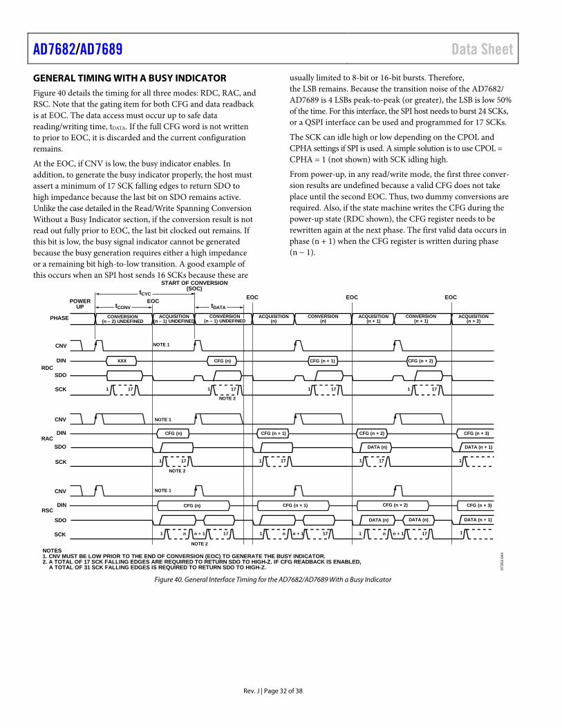
AD7682/AD7689 Data Sheet
Rev. J | Page 32 of 38
GENERAL TIMING WITH A BUSY INDICATOR Figure 40 details the timing for all three modes: RDC, RAC, and RSC. Note that the gating item for both CFG and data readback is at EOC. The data access must occur up to safe data reading/writing time, tDATA. If the full CFG word is not written to prior to EOC, it is discarded and the current configuration remains.
At the EOC, if CNV is low, the busy indicator enables. In addition, to generate the busy indicator properly, the host must assert a minimum of 17 SCK falling edges to return SDO to high impedance because the last bit on SDO remains active. Unlike the case detailed in the Read/Write Spanning Conversion Without a Busy Indicator section, if the conversion result is not read out fully prior to EOC, the last bit clocked out remains. If this bit is low, the busy signal indicator cannot be generated because the busy generation requires either a high impedance or a remaining bit high-to-low transition. A good example of this occurs when an SPI host sends 16 SCKs because these are
usually limited to 8-bit or 16-bit bursts. Therefore, the LSB remains. Because the transition noise of the AD7682/ AD7689 is 4 LSBs peak-to-peak (or greater), the LSB is low 50% of the time. For this interface, the SPI host needs to burst 24 SCKs, or a QSPI interface can be used and programmed for 17 SCKs.
The SCK can idle high or low depending on the CPOL and CPHA settings if SPI is used. A simple solution is to use CPOL = CPHA = 1 (not shown) with SCK idling high.
From power-up, in any read/write mode, the first three conver-sion results are undefined because a valid CFG does not take place until the second EOC. Thus, two dummy conversions are required. Also, if the state machine writes the CFG during the power-up state (RDC shown), the CFG register needs to be rewritten again at the next phase. The first valid data occurs in phase (n + 1) when the CFG register is written during phase (n − 1).
ACQUISITION(n – 1) UNDEFINED
ACQUISITION(n)
ACQUISITION(n + 1)
ACQUISITION(n + 2)PHASE
POWERUP
EOCEOC
START OF CONVERSION(SOC)
EOC EOC
CONVERSION(n)
CONVERSION(n + 1)
CONVERSION(n – 2) UNDEFINED
tCONV
tCYC
tDATA
CNV
CNV
CNV
DINRDC
RAC
RSC
SDO
NOTES1. CNV MUST BE LOW PRIOR TO THE END OF CONVERSION (EOC) TO GENERATE THE BUSY INDICATOR.2. A TOTAL OF 17 SCK FALLING EDGES ARE REQUIRED TO RETURN SDO TO HIGH-Z. IF CFG READBACK IS ENABLED, A TOTAL OF 31 SCK FALLING EDGES IS REQUIRED TO RETURN SDO TO HIGH-Z.
DIN
SDO DATA (n + 1)DATA (n)
DATA (n) DATA (n) DATA (n + 1)
DIN CFG (n) CFG (n + 2)CFG (n + 1) CFG (n + 3)
SDO
SCK 1 1 1 1
SCK 1 n n + 1 17
17 17 17 17
17 17 17
1 n n + 1 17 1 n n + 1 17
SCK 1 1 1 1
1
XXX
NOTE 1
NOTE 1
NOTE 1
NOTE 2
NOTE 2
NOTE 2
CFG (n) CFG (n + 1) CFG (n + 2)
CFG (n) CFG (n + 1) CFG (n + 2) CFG (n + 3)
CONVERSION(n – 1) UNDEFINED
0735
3-04
4
Figure 40. General Interface Timing for the AD7682/AD7689 With a Busy Indicator

Data Sheet AD7682/AD7689
Rev. J | Page 33 of 38
CHANNEL SEQUENCER The AD7682/AD7689 include a channel sequencer useful for scanning channels in a repeated fashion. Channels are scanned as singles or pairs, with or without the temperature sensor, after the last channel is sequenced.
The sequencer starts with IN0 and finishes with IN[7:0] set in CFG[9:7]. For paired channels, the channels are paired depend-ing on the last channel set in CFG[9:7]. Note that in sequencer mode, the channels are always paired with the positive input on the even channels (IN0, IN2, IN4, and IN6), and with the negative input on the odd channels (IN1, IN3, IN5, and IN7). For example, setting CFG[9:7] = 110 or 111 scans all pairs with the positive inputs dedicated to IN0, IN2, IN4, and IN6.
CFG[2:1] are used to enable the sequencer. After the CFG register is updated, DIN must be held low while reading data out for Bit 13, or the CFG register begins updating again.
Note that while operating in a sequence, some bits of the CFG register can be changed. However, if changing CFG[11] (paired or single channel) or CFG[9:7] (last channel in sequence), the sequence reinitializes and converts IN0 (or IN0/IN1 pairs) after the CFG register is updated.
Figure 41 details the timing for all three modes without a busy indicator. Refer to the Read/Write Spanning Conversion Without a Busy Indicator section and the Read/Write Spanning
Conversion Without a Busy Indicator section for more details. The sequencer can also be used with the busy indicator and details for these timings can be found in the General Timing with a Busy Indicator section and the Read/Write Spanning Conversion with a Busy Indicator section.
For sequencer operation, the CFG register must be set during the (n − 1) phase after power-up. On phase (n), the sequencer setting takes place and acquires IN0. The first valid conversion result is available at phase (n + 1). After the last channel set in CFG[9:7] is converted, the internal temperature sensor data is output (if enabled), followed by acquisition of IN0.
Examples
With all channels configured for unipolar mode to GND, including the internal temperature sensor, the sequence scans in the following order:
IN0, IN1, IN2, IN3, IN4, IN5, IN6, IN7, TEMP, IN0, IN1, IN2…
For paired channels with the internal temperature sensor enabled, the sequencer scans in the following order:
IN0, IN2, IN4, IN6, TEMP, IN0…
Note that IN1, IN3, IN5, and IN7 are referenced to a GND sense or VREF/2, as detailed in the Input Configurations section.
ACQUISITION(n – 1) UNDEFINED
ACQUISITION(n), IN0
ACQUISITION(n + 1), IN1
ACQUISITION(n + 2), IN2PHASE
POWERUP
EOCEOC
SOC
EOC EOC
CONVERSION(n – 1) UNDEFINED
CONVERSION(n), IN0
CONVERSION(n + 1), IN1
CONVERSION(n – 2) UNDEFINED
tCONV
tCYC
tDATA
CNV
CNV
CNV
DIN
SDO
XXX
MSBXXX
MSBXXX
NOTES1. CNV MUST BE HIGH PRIOR TO THE END OF CONVERSION (EOC) TO AVOID THE BUSY INDICATOR.2. A TOTAL OF 16 SCK FALLING EDGES ARE REQUIRED TO RETURN SDO TO HIGH-Z. IF CFG READBACK IS ENABLED, A TOTAL OF 30 SCK FALLING EDGES IS REQUIRED TO RETURN SDO TO HIGH-Z.
DATA IN0DATA (n – 1)XXX
DATA (n – 1)XXX
DATA (n – 1)XXX
DATA (n – 1)XXX
DATA (n – 2)XXX
DATA (n – 2)XXX
DATA (n – 2)XXX
DATA (n – 2)XXX
DATA (n – 3)XXX
DIN
SDO DATA IN1DATA IN0
DATA IN0 DATA IN0 DATA IN1
DIN CFG (n) CFG (n)
SDO
SCK 1
NOTE 1
16 16 16 16
NOTE 2
NOTE 2
NOTE 22
1 1 1
SCK 1 16 16 16n n n nn + 1 n + 1 n + 11 1
SCK 1 1 1 161616 1
1
CFG (n)RDC
RAC
RSC
CFG (n)07
353-
046
Figure 41. General Channel Sequencer Timing Without a Busy Indicator

AD7682/AD7689 Data Sheet
Rev. J | Page 34 of 38
READ/WRITE SPANNING CONVERSION WITHOUT A BUSY INDICATOR This mode is used when the AD7682/AD7689 are connected to any host using an SPI, serial port, or FPGA. The connection diagram is shown in Figure 42, and the corresponding timing is given in Figure 43. For the SPI, the host must use CPHA = CPOL = 0. Reading/writing spanning conversion is shown, which covers all three modes detailed in the Digital Interface section. For this mode, the host must generate the data transfer based on the conversion time. For an interrupt driven transfer that uses a busy indicator, refer to the Read/Write Spanning Conversion with a Busy Indicator section.
A rising edge on CNV initiates a conversion, forces SDO to high impedance, and ignores data present on DIN. After a conversion initiates, it continues until completion, irrespective of the state of CNV. CNV must be returned high before the safe data transfer time (tDATA), and held high beyond the conversion time (tCONV) to avoid generation of the busy signal indicator.
After the conversion is complete, the AD7682/AD7689 enter the acquisition phase and power-down. When the host brings CNV low after tCONV (maximum), the MSB enables on SDO. The
host also must enable the MSB of the CFG register at this time (if necessary) to begin the CFG update. While CNV is low, both a CFG update and a data readback take place. The first 14 SCK rising edges are used to update the CFG, and the first 15 SCK falling edges clock out the conversion results starting with MSB − 1. The restriction for both configuring and reading is that they both must occur before the tDATA time of the next conversion elapses. All 14 bits of CFG[13:0] must be written or they are ignored. In addition, if the 16-bit conversion result is not read back before tDATA elapses, it is lost.
The SDO data is valid on both SCK edges. Although the rising edge can capture the data, a digital host using the SCK falling edge allows a faster reading rate, provided it has an acceptable hold time. After the 16th (or 30th) SCK falling edge, or when CNV goes high (whichever occurs first), SDO returns to high impedance.
If CFG readback is enabled, the CFG register associated with the conversion result is read back MSB first following the LSB of the conversion result. A total of 30 SCK falling edges is required to return SDO to high impedance if this is enabled.
MISO
MOSI
SCK
SSCNV
FOR SPI USE CPHA = 0, CPOL = 0.
SCK
SDO
DIN
AD7682/AD7689
DIGITAL HOST
0735
3-03
6
Figure 42. Connection Diagram for the AD7682/AD7689 Without a Busy Indicator
UPDATE (n)CFG/SDO
UPDATE (n + 1)CFG/SDO
ACQUISITION (n)ACQUISITION(n - 1)
MSB
1 2
BEGIN DATA (n – 1)
BEGIN CFG (n + 1)
CFGMSB
14 15
SEE NOTE
SEE NOTE
NOTES1. THE LSB IS FOR CONVERSION RESULTS OR THE CONFIGURATION REGISTER CFG (n – 1) IF 15 SCK FALLING EDGES = LSB OF CONVERSION RESULTS. 29 SCK FALLING EDGES = LSB OF CONFIGURATION REGISTER. ON THE 16TH OR 30TH SCK FALLING EDGE, SDO IS DRIVEN TO HIGH IMPENDANCE.
16/30
CONVERSION (n)
END DATA (n – 1)
END CFG (n + 1)
CFGLSB X X
> tCONV
LSB
SCK
CNV
DIN
SDO
14 15 16/30
CONVERSION (n – 1)
END DATA (n – 2)
END CFG (n)
CFGLSB X X
tCONV
tDATAtCNVH
tDATA
tDIStDIS
tENtDSDOtHSDO
tHDINtSDINtCLSCK
tENtEN
tSCKtSCKH
tSCKL
tDIStDIS
tCONV
LSB
tACQ
tCYC
(QUIETTIME)
(QUIETTIME)
EOC EOC
RETURN CNV HIGHFOR NO BUSY
RETURN CNV HIGHFOR NO BUSY
0735
3-03
7
Figure 43. Serial Interface Timing for the AD7682/AD7689 Without a Busy Indicator

Data Sheet AD7682/AD7689
Rev. J | Page 35 of 38
READ/WRITE SPANNING CONVERSION WITH A BUSY INDICATOR This mode is used when the AD7682/AD7689 are connected to any host using an SPI, serial port, or FPGA with an interrupt input. The connection diagram is shown in Figure 44, and the corresponding timing is given in Figure 45. For the SPI, the host must use CPHA = CPOL = 1. Reading/writing spanning con-version is shown, which covers all three modes detailed in the Digital Interface section.
A rising edge on CNV initiates a conversion, ignores data present on DIN, and forces SDO to high impedance. After the conversion initiates, it continues until completion, irrespective of the state of CNV. CNV must be returned low before the safe data transfer time (tDATA), and then held low beyond the conversion time (tCONV) to generate the busy signal indicator. When the conversion is complete, SDO transitions from high impedance to low (data ready), and with a pull-up to VIO, SDO can be used to interrupt the host to begin data transfer.
After the conversion is complete, the AD7682/AD7689 enter the acquisition phase and power-down. The host must enable the MSB of the CFG register at this time (if necessary) to begin
the CFG update. While CNV is low, both a CFG update and a data readback take place. The first 14 SCK rising edges are used to update the CFG register, and the first 16 SCK falling edges clock out the conversion results starting with the MSB. The restriction for both configuring and reading is that they both occur before the tDATA time elapses for the next conversion. All 14 bits of CFG[13:0] must be written or they are ignored. If the 16-bit conversion result is not read back before tDATA elapses, it is lost.
The SDO data is valid on both SCK edges. Although the rising edge can capture the data, a digital host using the SCK falling edge allows a faster reading rate, provided it has an acceptable hold time. After the optional 17th (or 31st) SCK falling edge, SDO returns to high impedance. If the optional SCK falling edge is not used, the busy feature cannot be detected, as described in the General Timing with a Busy Indicator section.
If CFG readback is enabled, the CFG register associated with the conversion result is read back MSB first following the LSB of the conversion result. A total of 31 SCK falling edges is required to return SDO to high impedance if this is enabled.
AD7682/AD7689
MISO
MOSI
SCK
SS
SDO
VIO
FOR SPI USE CPHA = 1, CPOL = 1.
SCK
CNV
DIN
DIGITAL HOST
IRQ
0735
3-03
8
Figure 44. Connection Diagram for the AD7682/AD7689 with a Busy Indicator
SCK
ACQUISITION (n) ACQUISITION(n + 1)
CNV
DIN
SDO MSB MSB– 1
1 2
BEGIN DATA (n – 1)
BEIGN CFG (n + 1)
CFGMSB
LSB+ 1 LSB
1515
SEE NOTE
SEE NOTE
NOTES:1. THE LSB IS FOR CONVERSION RESULTS OR THE CONFIGURATION REGISTER CFG (n – 1) IF 16 SCK FALLING EDGES = LSB OF CONVERSION RESULTS. 30 SCK FALLING EDGES = LSB OF CONFIGURATION REGISTER. ON THE 17TH OR 31st SCK FALLING EDGE, SDO IS DRIVEN TO HIGH IMPENDANCE. OTHERWISE, THE LSB REMAINS ACTIVE UNTIL THE BUSY INDICATOR IS DRIVEN LOW.
1616 17/31
17/31
CONVERSION (n)CONVERSION (n – 1)
(QUIETTIME)
END DATA (n – 2) END DATA (n – 1)
END CFG (n + 1)END CFG (n)
XX X X X X
tDATA
UPDATE (n + 1)CFG/SDO
LSB+ 1 LSB
CONVERSION (n – 1) (QUIETTIME)
UPDATE (n)CFG/SDO
tCYC
tACQ
tHDIN
tHSDOtDSDO
tSDIN
tDATA
tCONV
tCNVH
tDIS
tDIS
tDIS tEN
tEN tEN
CFGMSB –1
tSCKtSCKH
tSCKL07
353-
039
Figure 45. Serial Interface Timing for the AD7682/AD7689 with a Busy Indicator

AD7682/AD7689 Data Sheet
Rev. J | Page 36 of 38
APPLICATIONS INFORMATION LAYOUT The printed circuit board (PCB) that houses the AD7682/ AD7689 must be designed so that the analog and digital sections are separated and confined to certain areas of the board. The pin configuration of the AD7682/AD7689, with all its analog signals on the left side and all its digital signals on the right side, eases this task.
Avoid running digital lines under the device because these couple noise onto the die unless a ground plane under the AD7682/AD7689 is used as a shield. Fast switching signals, such as CNV or clocks, must not run near analog signal paths. Avoid crossover of digital and analog signals.
Use at least one ground plane. It can be common or split between the digital and analog sections. In the latter case, join the planes underneath the AD7682/AD7689.
The AD7682/AD7689 voltage reference input, REF, has a dynamic input impedance and must be decoupled with minimal parasitic inductances. This is achieved by placing the reference decoupling ceramic capacitor close to (ideally, right up against)
the REF and GND pins and connecting them with wide, low impedance traces.
Finally, the power supplies of the AD7682/AD7689 (VDD and VIO) must be decoupled with ceramic capacitors, typically 100 nF, placed close to the AD7682/AD7689, and connected using short, wide traces to provide low impedance paths and to reduce the effect of glitches on the power supply lines.
The AN-617 Application Note has information on PCB layout and assembly. This information is particularly important for guiding customers who do not have experience with WLCSP.
EVALUATING THE AD7682/AD7689 PERFORMANCE Other recommended layouts for the AD7682/AD7689 are outlined in the documentation of the evaluation board for the AD7682/AD7689 (EVAL-AD7682EDZ/EVAL-AD7689EDZ). The evaluation board package includes a fully assembled and tested evaluation board, documentation, and software for controlling the board from a PC via the converter and evaluation development data capture board, EVAL-CED1Z.

Data Sheet AD7682/AD7689
Rev. J | Page 37 of 38
OUTLINE DIMENSIONS
0.50BSC
0.500.400.30
0.300.250.20
COMPLIANT TO JEDEC STANDARDS MO-220-WGGD-11.
4.104.00 SQ3.90
0.800.750.70 0.05 MAX
0.02 NOM
0.20 REF
0.20 MIN
COPLANARITY0.08
2.652.50 SQ2.35
1
20
610
11
15
16
5
BOTTOM VIEWTOP VIEW
SIDE VIEWFOR PROPER CONNECTION OFTHE EXPOSED PAD, REFER TOTHE PIN CONFIGURATION ANDFUNCTION DESCRIPTIONSSECTION OF THIS DATA SHEET.
09-0
4-20
18-C
EXPOSEDPAD
PKG
-003
578
P IN 1IN D ICATO R AR E A OP T IO NS(SEE DETAIL A)
DETAIL A(JEDEC 95)
PIN 1INDICATOR
AREA
SEATINGPLANE
Figure 46. 20-Lead Lead Frame Chip Scale Package [LFCSP]
4 mm × 4 mm Body and 0.75 mm Package Height (CP-20-10)
Dimensions shown in millimeters
A
B
C
D
E
2.4302.390 SQ2.350
123456789
BOTTOM VIEW(BALL SIDE UP)
TOP VIEW(BALL SIDE DOWN)
BALL A1IDENTIFIER
0.5600.5000.440
0.3300.3000.270SIDE VIEW
0.2300.2000.170
0.3000.2600.220
0.50 REF
0.50 REF
0.25 REF
0.433REF
COPLANARITY0.05
SEATINGPLANE
05-1
3-20
14-A
PKG
-004
466
Figure 47. 20-Ball Wafer Level Chip Scale Package [WLCSP]
(CB-20-12) Dimensions shown in millimeters

AD7682/AD7689 Data Sheet
Rev. J | Page 38 of 38
ORDERING GUIDE
Model1, 2 Integral Nonlinearity
No Missing Code
Temperature Range Package Description
Package Option
Ordering Quantity
AD7682BCPZ ±1.5 LSB maximum 16 bits −40°C to +85°C 20-Lead LFCSP CP-20-10 Tray, 490 AD7682BCPZRL7 ±1.5 LSB maximum 16 bits −40°C to +85°C 20-Lead LFCSP CP-20-10 Reel, 1,500 AD7682BCBZ-RL7 ±1.5 LSB maximum 16 bits −40°C to +85°C 20-Ball WLCSP CB-20-12 Reel, 1,500 AD7689ACPZ ±4 LSB maximum 15 bits −40°C to +85°C 20-Lead LFCSP CP-20-10 Tray, 490 AD7689ACPZRL7 ±4 LSB maximum 15 bits −40°C to +85°C 20-Lead LFCSP CP-20-10 Reel, 1,500 AD7689BCPZ ±1.5 LSB maximum 16 bits −40°C to +85°C 20-Lead LFCSP CP-20-10 Tray, 490 AD7689BCPZRL7 ±1.5 LSB maximum 16 bits −40°C to +85°C 20-Lead LFCSP CP-20-10 Reel, 1,500 AD7689BCBZ-RL7 ±1.5 LSB maximum 16 bits −40°C to +85°C 20-Ball WLCSP CB-20-12 Reel, 1,500 AD7689CCPZ ±2 LSB maximum 16 bits −40°C to +125°C 20-Lead LFCSP CP-20-10 Tray, 490 AD7689CCPZRL7 ±2 LSB maximum 16 bits −40°C to +125°C 20-Lead LFCSP CP-20-10 Reel, 1,500 EVAL-AD7682EDZ Evaluation Board EVAL-AD7689EDZ Evaluation Board EVAL-CED1Z Converter Evaluation and
Development Board
1 Z = RoHS Complaint Part. 2 The EVAL-CED1Z controller board allows a PC to control and communicate with all Analog Devices evaluation boards whose model numbers end in EDZ.
©2008–2019 Analog Devices, Inc. All rights reserved. Trademarks and registered trademarks are the property of their respective owners. D07353-0-11/19(J)