Embed Size (px)
Citation preview

A 3.3 kW Onboard Battery Charger for PHEVs
Saeid Haghbin and Torbjorn Thiringer
Technical Report 2015:1
Department of Energy and Environment
Division of Electric Power Engineering
CHALMERS UNIVERSITY OF TECHNOLOGY
Goteborg, Sweden 2015


A 3.3 kW Onboard Battery Charger for PHEVs
Saeid Haghbin and Torbjorn Thiringer
Technical Report 2015:1
Department of Energy and Environment
Division of Electric Power Engineering
CHALMERS UNIVERSITY OF TECHNOLOGY
Goteborg, Sweden 2015

A 3.3 kW Onboard Battery Charger for PHEVs
Saeid Haghbin and Torbjorn Thiringer
Technical Report 2015:1
Department of Energy and Environment
Division of Electric Power Engineering
CHALMERS UNIVERSITY OF TECHNOLOGY
SE-412 96 Goteborg
Sweden
Telephone + 46 (0)31 772 16 44


Abstract
Onboard battery chargers are the favourable option by automotive industry
because of ease of usage and security of supply by drivers. It is desirable
to have a charger powerful enough to fill the battery in few minutes, but
available technology is not mature enough to support this requirement in
terms of power density and price. The chargers with an input voltage level
of 230 Vac and an input current of 16 A can provide slightly more than 3.3 kW
charging power. These devices are one of the widely used chargers for plug-in
vehicles because of the availability of the power source. The aim of this report
is to explain and demonstrate the specifications, the design methodology and
the performance analysis of a typical 3.3 kW battery charger.
The main specifications of a 3.3 kW battery charger is presented and
explained including the target efficiency level and power density. Usually
there are two power conversion stages in an onboard charger: an AC/DC
converter with unity power factor and an isolated DC/DC converter. One of
the most popular topologies for each converter is selected and explained in
detail including design examples.
The interleaved Boost AC/DC rectifier is one of the high efficiency and
compact topologies utilized for AC/DC conversion with unity power factor
iii

operation. However, there is a need for a line filter to meet the standard
requirements. The topology is presented and the main design steps are de-
scribed. The efficiency analysis of the converter shows that an efficiency
level of 98% is achievable. Standard regulations and filtering guidelines are
provided.
For the second stage, a transformer isolated full-bridge converter with
the phase-shifted control and zero voltage switching (ZVS) is described. The
theory of operation, the design equations, the components selection, the loss
analysis in context of a practical example are discussed and presented. The
proper ZVS operation needs an accurate design of the resonant tank that
adds extra complexity to the converter design. This part is explained in
detail including the main equations.
As the second example, the design and loss analysis of a 3.3 kW battery
charger is provided with an output voltage of 110 V dc. The aim of this part
is to provide design materials for implementation of a practical system as
future work.
iv

Contents
Abstract iii
1 Introduction 1
2 3.3 kW Onboard Chargers: Main Specifications 5
2.1 Practical example of the onboard battery charger used in Volvo
Car V60 PHEV . . . . . . . . . . . . . . . . . . . . . . . . . . 9
3 Interleaved Boost AC/DC Converter 11
3.1 Basic Boost converter . . . . . . . . . . . . . . . . . . . . . . . 12
3.2 Interleaved Boost converter . . . . . . . . . . . . . . . . . . . 15
3.3 Design of an interleaved Boost rectifier with an input current
of 16 A and a dc output of 450 V . . . . . . . . . . . . . . . . 16
3.3.1 Boost inductor selection . . . . . . . . . . . . . . . . . 16
3.3.2 Output capacitor selection . . . . . . . . . . . . . . . . 17
3.4 Semiconductor losses of interleaved Boost converter at 230V/16A
input supply condition . . . . . . . . . . . . . . . . . . . . . . 18
3.4.1 Conduction losses in input bridge rectifier . . . . . . . 18
3.4.2 Conduction losses in Mosfet switches . . . . . . . . . . 19
v

3.4.3 Output diodes conduction losses . . . . . . . . . . . . . 19
3.4.4 Total semiconductor losses of the interleaved Boost rec-
tifier with 230V/16A input . . . . . . . . . . . . . . . . 20
3.5 Regulatory standards and line filters . . . . . . . . . . . . . . 20
4 Transformer Isolated Phase-shifted Full-bridge Converter with
Zero Voltage Switching Operation 23
4.1 Initial condition t < t0 . . . . . . . . . . . . . . . . . . . . . . 26
4.2 Start of the right transition t0 < t < t1 . . . . . . . . . . . . . 28
4.3 Completion of the right leg transition t1 < t < t2 . . . . . . . . 29
4.4 The left leg transition t2 < t < t3 . . . . . . . . . . . . . . . . 29
4.5 The power transfer interval t3 < t < t4 . . . . . . . . . . . . . 32
4.6 Design of the resonant tank . . . . . . . . . . . . . . . . . . . 34
5 Design and Analysis of a 3.3 kW DC/DC Converter with a
dc Output Voltage of 600 V 37
5.1 Inductor current . . . . . . . . . . . . . . . . . . . . . . . . . . 39
5.2 Transformer calculations . . . . . . . . . . . . . . . . . . . . . 39
5.3 Output diodes calculations . . . . . . . . . . . . . . . . . . . . 43
5.4 Bridge Mosfet switches calculations . . . . . . . . . . . . . . . 44
5.5 Total loss calculations . . . . . . . . . . . . . . . . . . . . . . 45
5.6 Minimum primary current for a proper ZVS operation . . . . . 45
6 Design and Analysis of an Air-Cooled 3.3 kW Battery Charger
with an Input of 230 V/16 A and a dc Output Voltage of 110 V 47
vi

6.1 Interleaved Boost AC/DC rectifier with an input of 230 V/16A
and a dc output voltage of 400 V . . . . . . . . . . . . . . . . 48
6.2 Phase-shifted full-bridge DC/DC converter with ZVS with a
dc Output voltage of 110 V . . . . . . . . . . . . . . . . . . . 49
6.2.1 Transformer turns ratio selection . . . . . . . . . . . . 49
6.2.2 Output filter design . . . . . . . . . . . . . . . . . . . . 50
6.2.3 Transformer current calculations . . . . . . . . . . . . . 51
6.2.4 Resonance and ZVS operation . . . . . . . . . . . . . . 51
6.2.5 Output diodes and bridge Mosfet switches calculations 52
7 Conclusions and Some Future Work Suggestions 55
References 59
vii

Chapter 1
Introduction
Battery chargers have an important impact on the development of plug-in
vehicles. The charger is a bridge between the grid and the vehicle; this tie
imposes some requirements on the charger specifications towards the utility
grid and vehicle. It is expected to have the near unity power factor operation
and stay under certain level of harmonics during charge operation. Moreover,
the charger should withstand the transients and under or over voltage oper-
ation. The auto industry requires a high power density and efficient charger
that could tolerate extreme temperatures or vibrating environment and at
the same time a low price. Despite the fact that the electrical isolation is not
required by related standards, for safety reasons it is strongly recommended
or required for a charger with a power level of 3.3 kW that are widely used
in vehicle applications [1–3].
Usually there are two converter stages in the charger circuit: a front-
end AC/CD converter as the power factor corrector (PFC) and an isolated
DC/DC stage. There are different topologies and variations for each stage
1

that one can refer to [4] for a full review and comparison. For the first stage,
an interleaved Boost AC/DC converter is selected and discussed here. For
the second stage, a transformer isolated full-bridge converter with a phase-
shifted control and zero voltage switching is described in the sequel.
The following headings are explained at the following sections for the
interleaved Boost Rectifier and phase-shifted full-bridge converter with ZVS
operation as the main power conversion stages of a 3.3 kW onboard charger:
• Providing a comprehensive list of technical publications and standards
as reference materials
• Short description of the converters basic operation
• Providing a design summary with practical examples
• Converters performance analysis in terms of components and losses
After this introduction, the main specifications of a 3.3 kW onboard
charger is explained in Section II. One example of an available charger is
presented to provide a realistic example. Section III is dedicated to the
interleaved Boost rectifier. Theory of operation, basic design equations, a
practical example and some simulation results are presented in this section.
The next section is devoted to the full-bridge DC/DC converter with a phase-
shifted control and ZVS operation. As the first practical example, the design
and analysis of a phase-shifted full-bridge DC/DC converter with an output
voltage of 600 V is described in Section V. The next example is a 3.3 kW
battery charger with 230 V/16 A input and 110 V dc output. The design of
2

the both interleaved Boost rectifier and phase-shifted full-bridge converter
are explained. The components selection and loss analysis are also provided.
3

4

Chapter 2
3.3 kW Onboard Chargers:
Main Specifications
The vehicle traction system is energized by a battery that can have a voltage
level of 200− 700 V . For passenger cars a voltage level of 300 V is common
while for bus and truck applications the higher voltage levels like 700 V can
be utilized. For instance, the main specifications of a 3.3 kW charger with a
nominal battery voltage of 300 V is presented in Table 2.1.
Usually the power level is limited by the available power from the utility
grid. For instance the maximum available power from a 230 V/16 A is
3520 W . For a charger with an efficiency level of 94% the output power
is 3.3 kW . From the design perspective the input voltage may have a wide
range, as is indicated in Table 2.1 for example, but the maximum line current
is 16 A. So the charger loads the grid with 16 A implying a variable power
for different line voltages.
The near unity power factor operation and a low value of total harmonic
5

Table 2.1: The main specifications of a 3.3 kW charger for a 300 V battery.
Input voltage from the utility grid (single-phase) 85− 270 VMaximum value of the input current from the grid 16 AAc line frequency range 47− 70 HzPower factor More than 99%Total harmonics distortion (THD) Less than 5%Output dc voltage 200− 470 VOutput dc voltage ripple (peak to peak) Less than 2 VMaximum output dc current 11 AMaximum output power 3.3 kWCharger efficiency Around 94%Cooling LiquidCoolant temperature −40 to + 70 ◦CAmbient temperature −40 to + 105 ◦CWeight/Volume Around 6kg/5L
distortion (THD) is easily achieved by using an active pre-regulator stage
including some line filters. The electro magnetic compatibility (EMC) issue
is another concern regarding the grid-connected chargers. There are plenty
of standards covering EMC and other similar topics like surge transients.
For instance one can refer to the IEC 61000-4 series that includes these
requirements. However, using a line filter to reduce EMC and transients is
the main solution to fulfill these requirements [5–7]. The filter design and its
optimality will be shortly discussed in the next section. The nominal battery
voltage in a passenger car can be around 300 V or 700 V . The tendency
is towards higher values because of a lower current in conductors. However,
insulation in devices and equipments makes it difficult to have higher values.
For a battery pack with a nominal voltage of 300 V the battery voltage
variations are wide. For example for a battery pack with a nominal value of
300 V , the battery voltage can vary between 275− 400 V depending on the
6

state of charge (SOC).
The charging profile of a battery has three stages. The first stage is the
bulk charge that a constant high current is injected to the battery. In this
stage the battery will be powered up to approximately 80% of its capacity.
The next stage is called absorption stage in which an absorption voltage is
applied to the battery to fill the rest of 20%. The current level is usually low
in this stage; and finally the float stage that the battery is kept charged by
applying a lower voltage and current compared to the absorption stage.
The impact of the charging profile on the charger is that the designer
shall size the conductors for high current charging (bulk) and adjust the
transformer turns ratio in the DC/DC converter to be able to reach the
desired output voltage for the absorption stage. Consequently, the maximum
current of the charger is not occurring simultaneously with highest output
voltage. For instance according to Table I, the charger maximum power can
be 11 A× 470 V = 5170 W ; instead the maximum power is 11 A× 300 V =
3300 W .
The charger efficiency is an important requirement especially when it
directly deals with the customer. The state of art of the available technology
for power electronic devices enables an efficiency level of around 94%. The
efficiency of the pre-regulator stage, PFC satge, is around 98% and for the
isolated DC/DC converter it can be around 96%. However, this performance
level is reported around nominal power with the input voltage around 230 V .
Deviations from this input voltage level or charging level reduces the charger
efficiency. This issue will be discussed further in the sequel.
The power density is another requirement that is equivalent to the weight
7

and volume. This requirement is extremely important for auto makers be-
cause of lack of space in the vehicle. To achieve a higher power density, the
current trend is to use liquid cooling, for instance water with glycol, to have
a compact package. The power electronics cooling system is usually indepen-
dent of the vehicle cooling system and it is the subject of research to unite
vehicle and power electronics cooling.
Table 2.2: Specifications of the 3 kW charger from Eltek utilized in V60PHEV.
Input voltage from the utility grid (single-phase) 85− 275 VMaximum value of input current from the grid 14 AAc line frequency range 45− 65 HzPower factor More than 99%Total harmonics distortion (THD) Less than 5%Output dc voltage 250− 420 VOutput dc voltage ripple (peak to peak) Less than 2 VMaximum output dc current 10 AMaximum output power 3 kWCharger efficiency 96% at 50% load
95% at 100% loadApplicable standards IEC 61851-1 EN 61000-6-1
EN 61000-6-2 EN 61000-6-3EN 61000-6-4 EN 61000-3-2
Cooling LiquidOperating temperature −40 to + 60 ◦CDimensions 49× 280× 120mm (IP20)
60× 355× 167mm (IP67)Weight 2.8 kg (IP20) and 4.3 kg (IP67)
The vehicle environment is harsh in terms of temperature variations and
vibrations. As is indicated in Table 2.1, the ambient temperature can be
somewhere between −40 to 105 ◦C. It is desirable to have a vehicle to be
able to operate in different climate conditions from north of Sweden to desert
8

areas in the middle of Iran, for example.
The highly vibrating environment of a vehicle requires special considera-
tion in packaging and installation of the battery charger. For instance, there
is a risk of component disconnection or loose connections over time. This
affects the device reliability and probability of failure. Usually the charger is
enclosed inside a metallic closure and there are some bumpers to reduce the
impact of vibration. In addition, the mechanical installation of the compo-
nents is designed to withstand relative requirements and standards.
2.1 Practical example of the onboard battery
charger used in Volvo Car V60 PHEV
The Norway-based Eltek Company supplies onboard battery chargers to
Volvo Car Corporation used in the V60 PHEV. The charger is a water cooled
device installed in an aluminum enclosure. The CAN controller in the charger
unit provides the communication protocol.
The charger is installed in two different mechanical enclosures: one with
ingress protection (IP) 20 and another one with IP 67. The device with
IP 20 weights 2.8 kg and the one with IP 67 weights 4.3 kg. The power
density in the first case is 1.8 kW/liter, which is very high. Table 2.2 provides
a summary of the charger specification [8].
9

10

Chapter 3
Interleaved Boost AC/DC
Converter
The ideal PFC pre-regulator emulates the converter as a resistor towards the
utility grid and transforms ac power to the charger acting as a resistor [9].
It is more convenient to approach the power balance for the modeling and
control of the converter. Fig. 3.1 shows the power in different parts of the
system. The parameters Ps(t), Pc(t) and PL(t) are instantaneous power of
the source, converter and load, subsequently. As is shown in this figure,
the converter should be able to store/supply a minimum level of power that
is the difference between the constant load power and instantaneous input
power. Consequently, this puts a limit on the minimum energy storage of
the converter that is the dc bus capacitor in this case. The dc bus capacitor
has a considerable impact on the converter power density; dc bus capacitor
reduction is still a subject of research to improve the converter power den-
sity. For instance by increasing the switching frequency or using interleaved
11

Vg sinωt
L
O
A
D
Idc=P/Vdc
Vdc
+
-
Power Converter
AC/DC with PFC
including Line
Filter
2P/Vg sinωt
tPP
tPtPS
w
w
2cos
sin2)( 2
-
== tPtPC
w2cos)( -= PtPL
=)(
Source Converter Load
PS(t)
t t t
PC(t) PL(t)
Figure 3.1: The main diagram of the Boost AC/DC converter in PFC appli-cations.
Single-Phase
AC Source
C
+
Q-
L
O
A
D
+
-
VrefVoltage
controller
Power Process
and
Current Control
iL
L
Gate
Signal
+
-
VinVo
Line
Filter
Figure 3.2: Power rectification with PFC based on Boost topology.
schemes one can reduce the capacitor size.
3.1 Basic Boost converter
The basic schematic diagram of a Boost converter in a PFC application is
shown in Fig. 3.2. The ac line voltage is rectified by a bridge rectifier. Switch
Q that can be a Mosfet for instance, charges the inductor and transfers power
to the output capacitor by using a proper switching operation. The inductor
is in series with the line impedance reducing the switching harmonics.
12

There are two control loops [10–18]: an output voltage controller and an
inner current controller. The voltage loop is slower than the inner current
controller. The bandwidth of the voltage control loop is around 2 − 20 Hz
and the bandwidth of the current controller is much faster, can be around 1/6
switching frequency [18]. It is intended to have a constant output voltage,
but there is a voltage ripple determined by the switching frequency and
components values. The task of the voltage control loop is to program the
input current to have a constant power with unity power factor from the ac
source. The deviation from reference output voltage indicates extra energy
or an energy deficit in the system in which the current level is adjusted by
the controller.
Different control strategies have been proposed for the Boost converter in
PFC application [18]. The voltage loop is usually a PI controller or type II
controller [10, 18]. A type II compensator has two poles (one at the origin)
and one zero, and the zero is placed somewhere between the poles. The trans-
fer function of this controller can be written as GC(s) = k (s/ωz+1)s(s/ωp+1)
where k
is a constant, ωz is the angular frequency of zero and ωp is teh angular fre-
quency of pole. The output of the voltage controller is the reference value
for the current controller. However, there are some enhancements like feed-
forwad terms to improve the load and line dynamics. The Boost converter
can operate on three modes depending on the inductor current: continu-
ous conduction mode (CCM), discontinuous conduction mode (DCM) and
boundary conduction mode (BCM) [19–21]. In CCM the inductor current
will not reach to zero when the current is at its peak value, but in discontin-
uous conduction mode the inductor current is zero for a while during each
13

switching period. The BCM is the critical point which CCM turns into to
DCM. The design rule for inductor value is different for CCM and DCM.
The inductor value for CCM can be determined as [20]
LCCM =Vo
4fs∆I(3.1)
where Vo, fs and ∆I are output voltage, switching frequency and designed
current ripple (peak to peak) in the inductor consequently. The inductance
value for DCM can be determined as [20]
LDCM =Vg (1− Vg
Vo)
fs∆IP(3.2)
where Vg is the maximum line voltage and ∆IP is the current ripple when
the line current is at its maximum value.
The output voltage ripple is
∆Vo =Po
2ωCo(3.3)
where ω, Co and Po are the line angular frequency, the output dc bus capacitor
and the output power respectively.
Despite the converter operation mode, there are different ways for the
current control inside the fast inner loop. The average current mode con-
trol, peak current mode control and boundary current mode control are the
main current mode control schemes. All of these three schemes are used for
different applications and there are commercially available controllers. The
average current mode control (ACMC) [18] is the dominant method for high
14

power applications because of its robustness to noise and its stable operation;
there is no problem with instability for duty cycles higher than 0.5 as is the
case for the peak current mode control.
3.2 Interleaved Boost converter
There are different circuit topologies that can be utilized as the PFC pre-
regulator. However, the Boost converter is one the most used options for
this application. There are different varieties and improvements to the basic
Boost converter to achieve a performance closer to the ideal AC/DC con-
verter.
The interleaved Boost rectifier is an interesting configuration from the
Boost converter family providing some advantages over the basic topology
[20–25]. There are two energy storage inductors with two independent switches
and diodes that share the same bridge rectifier at the input side and the same
dc bus capacitor, as is shown in Fig. 3.3. The switching functions are inter-
leaved which significantly reduces the input line and output ripples. It simply
can reduce the ripple to half when the duty cycle is half. In addition, in-
terleaving provides the benefits for parallel converter operation for higher
power applications. The idea of interleaving is that two inductors have op-
posite ripple directions; they cancel out each other in the line current.
15

C
+
Q1 Q2-
L
O
A
D
+-
VrefVoltage
controller
Power Process
and
Current Control
iL1 iL2
L1
L2
S1,2Gate
Signals
+
-
VinVo
Single-Phase
AC Source
Line
Filter
Figure 3.3: Interleaved Boost rectifier as the front end converter.
3.3 Design of an interleaved Boost rectifier
with an input current of 16 A and a dc
output of 450 V
The design steps of an interleaved Boost rectifier with an input of 16 A and
an output voltage of 450 V is explained in this section. It is assumed that the
rms value of the input voltage can be up to 260 V . The switching frequency
is pre-selected to 180 kHz in this case. Moreover, it is intended to operate
the converter in CCM.
3.3.1 Boost inductor selection
By using (3.1) and selecting L1 = L2 = 600 uH , the current ripple is ∆I =
1 A which is around 5% of the peak value of the inductor current.
16

3.3.2 Output capacitor selection
The output capacitor is usually selected to hold the output voltage for a
certain time interval when there is a transient or shortage in the input grid
voltage. For instance one can ask for a holding time of half a cycle, which is
10 ms. In addition, it is desirable to limit the voltage ripple in a certain level
that is ∆Vo defined as the difference between the peak value and nominal
value Vo. By selecting C = 780 uF and using (3.3), the output voltage ripple
is ∆Vo = 18 V when the input power is 260× 16 = 4160 W .
The stored energy in this capacitor is WC = 12CV 2 = 101.25 J which can
supply the load for slightly more than 24 ms. The maximum value of the
stored energy in each Boost inductor is 12Li2 = 0.5×600u×(8
√2)2 = 38.4mJ .
The stored energy in each inductor is much lower than the stored energy in
the output capacitor and it can be neglected.
The rms value of the capacitor current can be calculated as [21] IC,rms =
Iof(α) where α = Vg
Vo= 260
√2
450= 0.8. The function f has a complicated
analytical form which one can see [21] for detailed explanations. However,
in this case α = 0.8 and the capacitor rms current is IC,rms = Iof(α) =
9.2× 0.8 = 7.36 A.
17

3.4 Semiconductor losses of interleaved Boost
converter at 230V/16A input supply con-
dition
The semiconductor components in an interleaved Boost rectifier are the input
bridge rectifier (four diodes), the Boost switches that are of the Mosfet type
in this case and output rectifier diodes. The semiconductor losses are usually
divided into switching losses and conduction losses. For the input bridge
rectifier, the commutation is performed with line frequency, i.e. 50 Hz, so
there is no high frequency switching losses. For the Boost switches and output
diodes by using SiC devices one can ignore switching losses. Consequently,
the semiconductor losses are simplified to conduction losses.
For diodes, a simplified equation for conduction losses can be written as
PC,Diode = ID,aveVD where ID,ave is the average value of the diode current
and VD is the diode voltage drop. For a Mosfet, the conduction loss can be
written as PC,Mosfet = RdsI2Mosfet,rms where Rds is the Mosfet on resistance
and IMosfet,rms is the rms value of the Mosfet current.
3.4.1 Conduction losses in input bridge rectifier
the conduction losses in the input bridge diodes can be written as PC,Diode =
4ID,aveVD. Here it is assumed that VD = 1 V and the average value of the
current is
ID,ave =1
2π
∫ π
0
Igsin(θ)dθ (3.4)
18

where Ig is the maximum value of the input current. For this converter with
a current level of 16 A (rms), the average value of the current is ID,ave =Igπ=
7.2 A. Consequently, the diodes conduction losses are PC,Diode = 4×7.2×1 =
28.8 W .
3.4.2 Conduction losses in Mosfet switches
for an interleaved Boost rectifier, two parallel switches have ideally the same
rms current. The rms value of each Mosfet can be written as [26]
IMosfet,rms =1
2
Ig√2
√
1−8
3π
Vg
Vo
(3.5)
where 12is expressing two interleaved Mosfet switches. For each Mosfet, the
rms current is IMosfet,rms =1216√
1− 83π
230√2
450= 4.97 A. The conduction loss
in each Mosfet is PC,Mosfet = 0.25× 4.972 = 6.17 W where Rds = 0.25 Ohm.
For two switches, the total conduction losses are 12.34 W .
3.4.3 Output diodes conduction losses
there are two output diodes that share the current which each have an average
of half of the load dc current. The average value of the load current is
230×16/450 = 8.17 A. If we assume VD = 1 V , the didoes conduction losses
are PC,Fast Diodes = 8.17× 1 = 8.17 W .
19

3.4.4 Total semiconductor losses of the interleaved Boost
rectifier with 230V/16A input
the total losses can be calculated as
PInterleaved,Semiconductors = PC,Diodes + PC,Mosfets + PC,Fast Diodes =
28.8 + 12.34 + 8.17 = 49.31 W
(3.6)
The total semiconductor losses are around 1.3% of the input power (230 ×
16 = 3680 W ).
3.5 Regulatory standards and line filters
For the grid connected chargers there are two types of regulatory standards:
standards addressing harmonics (lower frequency range) and standards deal-
ing with higher frequencies concerning EMC. The main objectives of low
frequency standards like IEC 6100-3-2 [1] are power factor, harmonics and
THD. Above mentioned Boost topologies will easily pass the low frequency
requirements if they operate properly. However, it is more challenging to
cope with EMC issues.
There are standards concerning higher frequencies like IEC 61851-21-1 [2]
that is dedicated to onboard battery chargers in vehicle applications. The
frequency range of the standards addressing EMC is 150 kHz − 30 MHz.
The high frequency noise is around the switching frequency and its multiples.
For instance, one can choose the switching frequency lower than 150 kHz to
be under the 150 kHz limit. However, a line filter shall be utilized to make
20

EMI Filter
.
.
LC
LC
LD
LD
CX1CX2
CY
CY
Figure 3.4: Typical EMI filter to fulfill standard requirement regarding highfrequency noise.
sure that the device can fulfill this requirement. Both the common mode
noise and differential mode noise should be considered in the filter design.
Fig. 3.4 shows a typical EMI filter where there are differential mode fil-
tering and common mode filtering stages [27]. In addition, there might be
some protective devices like voltage suppressors or surge arrestors to cope
with transients.
The filter has an important impact on the total power density; it is ideal
to optimize the filter and PFC pre-regulator to have even better performance
in terms of power density. For instance, one can reduce the size of the Boost
inductor which would give a higher current ripple. This can be compensated
by having a larger filter. So, it is an optimization task to find out a proper
compromise between the filter and PFC pre-regulator [16].
21

22

Chapter 4
Transformer Isolated
Phase-shifted Full-bridge
Converter with Zero Voltage
Switching Operation
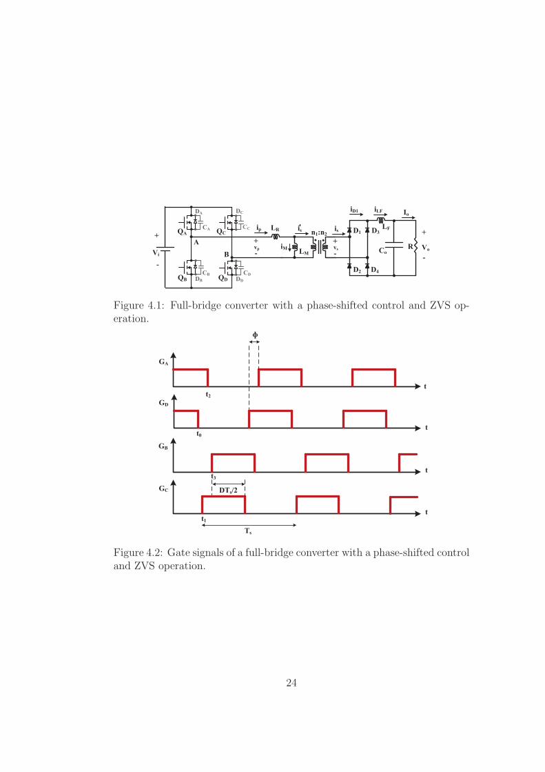
Fig. 4.1 shows a schematic diagram of the full-bridge DC/DC converter with
a phase-shifted control and zero voltage switching capability [28–34]. The
control is performed by a proper turn on/off of four switches (QA − QD) in
the primary side bridge. Here it is assumed that the switches type is a power
Mosfet. Moreover, inside each Mosfet there are an anti-parallel diode and a
parasitic output capacitance that are utilized to perform the ZVS operation.
However, those two components can also be external devices.
The timing diagram of the gate control signals are depicted in Fig. 4.2.
There are two legs: A and B that each leg includes the upper and lower
23
+
-
CoVo
QA
QB
QC
QD
D1
D2
D3
D4
LF
ViR
LM
LR . .n1:n2CA
CB
CC
CD
+
-
DA DC
DB DD
ip
iM
is
iD1 iLF Io
+
-vs
+
-vp
A
B
is
Figure 4.1: Full-bridge converter with a phase-shifted control and ZVS op-eration.
GA
GD
GB
GC
t
t
t
t
t0
ɸ
Ts
DTs/2
t1
t2
t3
Figure 4.2: Gate signals of a full-bridge converter with a phase-shifted controland ZVS operation.
24

vi
+
- Transformer
Bridge
vi
+
- Transformer
Bridge
vi
+
- Transformer
Bridge
vi
+
- Transformer
Bridge
a) t<t0 b) t0<t<t1
c) t1<t<t2 d) t2<t<t3
vi
+
- Transformer
Bridge
vi
+
- Transformer
Bridge
e) t3<t<t4 f) t4<t<t5
Figure 4.3: A simple presentation of the switching status and timing for thephase-shifted ZVS converter.
Mosfet switches. The left leg includes QA and QB and the right leg includes
QC and QD. There are different ways to control the gate signals, but one
sophisticated method is to have a fixed duty cycle slightly less than 50%
for each leg. The blanking time between the upper and lower switches pro-
vides shoot-through protection and is also part of the ZVS operation. This
blanking time is determined by the designer to reach ZVS operation over a
large range of the load and input voltage. The phase-shift between the two
legs determines the power transfer from the input supply to the load. If this
phase-shift Φ is zero, the converter operates like a conventional hard-switched
one with a duty cycle of 1. For a Phase-shift angle of 180 degree, there is
no power transfer and the duty cycle is zero. The gate signals switching
25

times are shown in Fig. 4.2 which the important time instants are denoted
by t0 − t4. The definition of switching period Ts and the duty cycle D are
shown in the figure too. Fig. 4.3 shows the status of switches in different
time intervals according to the related gate signals. This figure depicts more
intuition of the switching operation. The converter operation is explained at
the following [28, 29].
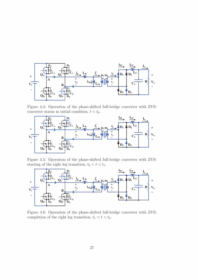
4.1 Initial condition t < t0
Suppose that QA and QD are conducting. Diodes D1 and D4 are conducting
and charging the output inductor LF while transferring power to the load.
The circuit diagram is shown in Fig. 4.4. The active part of the circuit is
in blue color. For instance, parasitic diodes and capacitors of the primary
bridge are not conducting. There is no stored energy in capacitor CD while
capacitor CC is fully charged with input supply voltage Vi. The same holds
for CA and CB. These capacitors in interaction with leakage inductance LR
performs the ZVS operation.
At full load, the transformer primary current is the maximum possible
value which is the reflected load current to the primary and the magnetiza-
tion current. The leakage inductance is usually much lower than the mag-
netization inductance, hence the voltage drop over the leakage inductance is
negligible.
26
+
-
CoVo
QA
QB
QC
QD
D1
D2
D3
D4
LF
ViR
LM
LR . .n1:n2CA
CB
CC
CD
+
-
DA DC
DB DD
ip
iM
is
iD1 iLF Io
+
-vs
+
-vp
A
B
is
Figure 4.4: Operation of the phase-shifted full-bridge converter with ZVS:converter status in initial condition, t < t0.
+
-
CoVo
QA
QB
QC
QD
D1
D2
D3
D4
LF
ViR
LM
LR . .n1:n2CA
CB
CC
CD
+
-
DA DC
DB DD
ip
iM
is
iD1 iLF Io
+
-vs
+
-vp
A
B
is
Figure 4.5: Operation of the phase-shifted full-bridge converter with ZVS:starting of the right leg transition, t0 < t < t1.
+
-
CoVo
QA
QB
QC
QD
D1
D2
D3
D4
LF
ViR
LM
LR . .n1:n2CA
CB
CC
CD
+
-
DA DC
DB DD
ip
iM
is
iD1 iLF Io
+
-vs
+
-vp
A
B
is
Figure 4.6: Operation of the phase-shifted full-bridge converter with ZVS:completion of the right leg transition, t1 < t < t2.
27

4.2 Start of the right transition t0 < t < t1
The right leg transition is starting by turning off QD as is depicted in Fig. 4.2
and 4.3. Assume that at t = t0 switch QD is commanded to the off state.
The magnetization current is usually much less than the full load current.
After t = t0 the stored energy in leakage inductance LR forces the current
to continue to flow through CC and CD until they change status from fully
charged to fully deployed and vice versa. The circuit diagram including
current path is shown in Fig. 4.5.
The stored energy in the leakage inductance should be higher than the
stored energy in the capacitors for a proper ZVS operation. For instance, at
light loads in which the leakage inductance can not supply this energy level,
the ZVS operation is lost. Usually the ZVS operation range is 50% of full
load (decided by the designer).
In this time interval the capacitors are charged and de-charged linearly
over time; consequently, the transformer primary voltage linearly decreases.
The transformer secondary voltage also decreases and in a certain point the
voltage value is equal to the output voltage. After this point, the voltage
over the output inductor changes its polarity and there is no power transfer
from the input supply to the load. Afterwards, the output inductor and the
output capacitor supply the load. At the end of this interval the transformer
primary voltage reaches zero voltage.
28

4.3 Completion of the right leg transition t1 <
t < t2
When CD is fully charged it will not take more current from the circuit. The
capacitor CC is ideally fully de-charged, so the current flows through diode
DC . This is the mechanism of the ZVS operation. If the gate signal of QC is
activated by the controller, QC is turned on lossless because the antiparallel
diode forces the switch’s voltage to a value close to zero. However, one needs
to make sure that the diode is conducting before the gate activation by a
proper component and controller selection.
Fig. 4.6 shows the circuit diagram in this case. After activation of QC
the diode is still conducting. The two devices share the current that lowers
the conduction loss. By turning on the Mosfet QC , the right leg transition
is finished and the circuit is ready to perform the left leg transition under
ZVS condition. The magnetization current is circulating through QA, QC
and DC .
When the right leg transition is finished, the transformer primary and
secondary voltages are zero and there is no power transfer to the load from
the input supply. The output inductor, LF , supplies the load and forces all
diodes at the output bridge, D1 −D4, to conduct and share the current.
4.4 The left leg transition t2 < t < t3
The left leg transition is initiated by the turning off of the QA gate signal at
t = t2. It is desired to turn off QA and turn on QB with a zero voltage. In
29

this moment the transformer primary current, ip(t2), is slightly less than the
transformer initial current, ip(t0), because of the losses. At t = t2 the Mosfet
channel stops to conduct the current and CA takes over the current flow.
Capacitor CB starts to supply the current simultaneously. Consequently, the
voltage at point A starts to decrease towards zero which is preparing for the
ZVS operation of QB. Fig. 4.7 shows the circuit configuration in this case.
The left leg transition has a different mechanism compared to the right
leg transition. All diodes in the secondary are conducting; this provides a
short circuit to the transformer. Consequently, unlike the right leg transition,
the impact of the load current on the primary side is removed. Consequently
CA and CB are de-charging and charging with a resonant mechanism instead
of a linear one. These two capacitors and transformer leakage inductance,
LR, are part of a resonant circuit. The energy source for this series resonance
circuit is provided by the leakage inductance with the initial current of ip(t2).
By solving the circuit in this time interval one can calculate the leakage
inductance current at t = t3 by the following equation as [28, 29]
t3 − t2 =1
ωRarcsin(
ViZi
ip(t2)) (4.1)
where ZR and ωR are the resonant tank circuit impedance and self-oscillating
frequency defined as [28, 29]
ZR =
√
LR
CR
(4.2)
ωR =1√
LRCR
. (4.3)
30

+
-
CoVo
QA
QB
QC
QD
D1
D2
D3
D4
LF
RLM
LR . .n1:n2CA
CB
CC
CD
+
-
DA DC
DB DD
ip
iM
is
iD1 iLF Io
+
-vs
+
-vp
A
B
is
Figure 4.7: Operation of the phase-shifted full-bridge converter with ZVS:the left leg transition, t2 < t < t3.
+
-
CoVo
QA
QB
QC
QD
D1
D2
D3
D4
LF
ViR
LM
LR . .n1:n2CA
CB
CC
CD
+
-
DA DC
DB DD
ip
iM
is
iD1 iLF Io
+
-vs
+
-vp
A
B
is
Figure 4.8: Operation of the phase-shifted full-bridge converter with ZVS:the power transfer interval, t3 < t < t4.
31

The equivalent resonant capacitance can be selected as [28, 29]
CR =8
3Coss + CT (4.4)
where Coss is the Mosfet output capacitance and CT is the transformer input
capacitance. During each transition, two switches capacitors are involved and
these capacitors have not a constant value. So, they are approximated by
83Coss. The transformer capacitance is not negligible in many high frequency
applications that one needs to consider it in the equation.
The left leg transition time is longer than the right leg transition since
the mechanism is different. In conventional controllers it is possible to adjust
the right and left leg transition times independently.
4.5 The power transfer interval t3 < t < t4
At t = t3, Mosfet QB turns on under ZVS. This completes the right leg
transition. The transformer primary voltage changes to −Vi and the two
secondary diodes conduct and supply the load. The circuit configuration is
shown in Fig. 4.8. The transformer magnetization current increases in this
interval. Note that the polarity of the transformer voltage is changed. As
one can see from Fig. 4.2 and 4.3 at t = t4, Mosfet QC turns off that is the
same as the first interval. From this moment the circuit is operating like
before. The converter waveforms are shown in 4.9.
32

iP(t)
t
IPI2 I1
-I2-IP
vP(t)
t
vi
-vi-vi
vs(t)
t
V’
i
vLF(t)
t
V’i-Vo
iLF(t)
t
iD1(t)
tiD3(t)
t
-V’
i
iM(t)
t
IM2
-IM2
IM1
-IM1
-I1
-Vo
V’i-Vo V’i-Vo
-Vo
t0 t3t4
t2
t1
ooII D+
ooII D-
oI
Figure 4.9: The waveforms of the full-bridge converter with phase-shiftedcontrol and ZVS operation.
33

4.6 Design of the resonant tank
As is mentioned earlier, the resonant tank condition controls the ZVS oper-
ation. Two conditions must be held by the resonance circuit: enough stored
inductive energy and allocation of enough time for the transition. The worse
condition is under light load or high voltage in the input. The resonant tank
components are LR and CR with a resonant frequency of ωR. The maximum
transition time should be less than one-fourth of the resonance period that
can be expressed as [28, 29]
tmax =1
4
2π
ωR=
π
2ωR(4.5)
The required energy in the capacitors can be written as
WC =1
2CRV
2i =
4
3Coss +
1
2CTV
2i . (4.6)
There is a factor of 4/3 in output capacitance of the Mosfet to somehow use
an estimated average value of the device capacitance. The stored inductive
energy is
WL(t) =1
2LRi
2p(t). (4.7)
One can calculate the required leakage inductance by the following equation
as
LR =1
( π2tmax
)2CR. (4.8)
34

In addition, the minimum load condition can be calculated as
iP,min =
√
CRV 2i
LR. (4.9)
Below this current, the stored energy in the inductor is less than the stored
energy in the capacitors that avoids proper ZVS operation of. The designer
can set the value of LR such that the ZVS is achieved up to a certain level
of the primary current such as 50% of the nominal load.
35

36

Chapter 5
Design and Analysis of a 3.3 kW
DC/DC Converter with a dc
Output Voltage of 600 V
The design procedure and analysis of a DC/DC converter with the specifica-
tions described in Table 5.1 is presented in this section. Some parameters are
specified in Table 5.1 and others will be selected by following the described
design procedure.
The output current can be calculated as 3300/600 = 5.5 A. The allowed
loss of the converter is 3300×0.05 = 165W . The loss includes semiconductor
losses in the input bridge and output rectifier plus transformer and output
inductor losses. By a proper operation of ZVS and utilizing SiC devices, the
semiconductor’s switching losses are close to zero and are neglected here.
The transformer turns ratio is defined as n = n1/n2 which n1 and n2 are
the number of turns in primary and secondary of the transformer. Here it
37

is assumed that n is given and n = 0.5. The input/output relation can be
described as
Vo = DVi
n(5.1)
where D is the effective duty cycle. For this converter the duty cycle is
D = 600× 0.5/450 = 0.666.
If the magnetization current is too high, then the converter can not op-
erate under peak current mode control; since the impact of load can not be
detected. The magnetization current should be lower than the inductor cur-
rent ripple reflected to the primary side. Assume that the converter is in the
boundary condition mode, then the peak load current should be more than
the maximum value of the magnetization current. Then this requirement can
be stated as IM < ∆Io/n. The required magnetization inductance can be
calculated as
LM >nDVi
4∆Iofs= (0.5× 0.666× 450)/(4× 0.55× 180000) = 0.375 mH (5.2)
It is assumed that the output current ripple is ∆Io = 0.1Io = 0.55 A. A
Table 5.1: Specifications of a 3.3 kW DC/DC converter with an outputvoltage of 600 V .
Input dc voltage, Vi 440− 460 VOutput power 3300 WOutput dc voltage, Vo 600 V dcSwitching frequency, fs 180 kHzOutput inductance, LF 600 uHTransformer turns ratio, n 0.5Efficiency more than 95%
38

tt0 t3 t4
Ts
D Ts/2iLF(t) ooII D+
ooII D-
oI
Figure 5.1: The waveform of the output inductor current.
magnetization inductance of 400 uH is selected here.
5.1 Inductor current
The inductor voltage can be written as
Vi/n− Vo = LF2∆IoDTs/2
. (5.3)
The inductor current ripple is calculated as ∆Io = 0.46 A for this converter.
Fig. 5.1 shows the current waveform.
The rms value of the inductor current can be calculated as
iLF,rms = Io
√
1 +1
3(∆IoIo
)2 (5.4)
which is equivalent to iLF,rms = 5.5√
1 + 13(0.555.5
)2 = 5.5 A in this case.
5.2 Transformer calculations
The transformer primary current is shown in Fig. 5.2. The peak value of the
current, IP , is the maximum load current reflected to the primary plus the
39

maximum value of the magnetization current, IM . The value of IM can be
calculated as
IM =DVi
4LMfs(5.5)
which in this case is IM = 0.666×4504×0.4mH×180kHz
= 1.04 A.
There are three important current levels in the transformer primary cur-
rent indicated as IP , I1 and I2 , as shown in Fig. 5.2. These currents can be
calculated as
IP = IM +Io +∆Io
n(5.6)
I1 = −IM +Io −∆Io
n(5.7)
I2 = IM +Io −∆Io
n(5.8)
where in this case they are equal to
• IP = 1.04 + (5.5 + 0.46)/0.5 = 12.96 A
• I1 = −1.04 + (5.5− 0.46)/0.5 = 9.03 A
• I2 = 1.04 + (5.5− 0.46)/0.5 = 11.11 A.
After some mathematical manipulation the rms value of the transformer
current on the primary side can be written as
I2P,rms =1
3(−IP + I2)
2D1 + (−IP + I2)IPD1 + I2PD1
+1
3(−I2 − I1)
2D2 + (−I2 − I1)I2D2 + I22D2
+1
3(−IP + I1)
2D + (−IP + I1)(−I1)D + I21D
(5.9)
40

iP(t)
t
IP
I2I1
-I2
-IP
-I1
t2t0
t3 t4
t0
Ts/2
Ts
D Ts/2
Figure 5.2: The waveform of the transformer primary current.
where parameters D, D1 and D2 are calculated as
D =t4 − t3Ts/2
(5.10)
D1 =t2
Ts/2(5.11)
D2 =t3 − t2Ts/2
. (5.12)
Moreover the following equation holds
D +D1 +D2 = 1. (5.13)
The right transition time can be calculated as t3 − t2 =14TR = 1
42πωR
= 40 ns.
Consequently, the value of D2 is 0.0145. For this converter the rms current
in the transformer primary side is calculated as 11.32 A.
The transformer secondary current is shown in Fig. 5.3. The peak value
of the current, IPS, is the maximum load current. There are three important
current levels in the transformer secondary current indicated as IPS, I1S and
41

iS(t)
t
IPS
I2SI1S
-I2S
-IPS
-I1S
t2t0
t3 t4
t0
Ts
D Ts/2
Figure 5.3: The waveform of the transformer secondary current.
I2S in Fig. 5.3. These currents can be calculated as
IPS = Io +∆Io (5.14)
I1S = Io −∆Io (5.15)
I2S = Io −∆Io − nIM (5.16)
which in this case are IPS = 5.5 + 0.46 = 5.96 A, I1S = 5.5 − 0.46 = 5.04 A
and I2S = 5.5 − 0.46 − 0.5 × 1.04 = 4.56 A. After some mathematical
manipulation the rms value of the transformer current in the secondary side
can be written as
I2S,rms =1
3(−IPS + I2S)
2D1 + (−IPS + I2S)IPSD1 + I2PSD1
+1
3(−I2S − I1S)
2D2 + (−I2S − I1S)I2SD2 + I22SD2
+1
3(−IPS + I1S)
2D + (−IPS + I1S)(−I1S)D + I21SD
(5.17)
For this converter the rms current in the transformer secondary side is 5.31 A.
42

iD1(t)
t
IPS
I2DS
t1t0 t3 t4 t0
Ts
D Ts/2
iD2(t)
t
IPS
t1t0 t3 t4 t0
I2DSI1S
Figure 5.4: The waveform of the output diodes.
iD1(t)
t
IPS
t0 t4 t0
I1SD Ts/2
Ts/2
Figure 5.5: The approximated waveform of output diode D1.
5.3 Output diodes calculations
The waveforms of the output diodes are shown in Fig. 5.4. During the power
transfer interval, the conducting diodes have the same current as the output
inductor. The waveforms show the detailed timing, but it is difficult to
calculate the exact amount of current. However, one can approximate the
waveform such that during the rest of time interval the diode current is half
of the inductor current. Fig. 5.5 shows the simplified diagram.
The diode D1 average current can be determined as
ID = [1
2(I1S + IPS)D
Ts
2+
1
2IPS(1−D)
Ts
2]/Ts = 2.24 A. (5.18)
43

The diode losses can be calculated as 4IDVD = 4× 2.24× 1 = 8.96 W . The
voltage drop of the diode is assumed to be 1 V and the resistance of the diode
is neglected. Moreover, by utilizing SiC diodes one can neglect the diodes
switching losses.
5.4 Bridge Mosfet switches calculations
By a proper design and operation of the converter, the Mosfet switching
losses are close to zero. In addition, the Mosfet body diode conducts for a
short period of time during the transition. Hence, it is possible to neglect the
losses related to that time interval. Consequently, it is a good approximation
to consider each Mosfet conducting during the power transfer interval in
which the current is equivalent to the transformer primary. Fig. 5.6 shows
the approximate waveform of a Mosfet.
The rms value of each Mosfet can be approximated as
IMos,rms =
√
m2D3T 2s
24+
mD2TsI14
+I21D
2(5.19)
where m = IP−I1DTS/2
. For this converter the Mosfet rms current is 6.38 A.
The Mosfet conduction loss can be approximated as RdsI2Mos,rms that gives
0.25× 6.382 = 10.17 W for each Mosfet. The total conduction losses of the
four Mosfets are 40.70 W for this converter.
44

iQ(t)
t
IP
I1D Ts/2
Ts
Figure 5.6: The approximated waveform of an input Bridge Mosfet.
5.5 Total loss calculations
The converter total losses are semiconductor losses and magnetic losses in the
transformer and output inductor. Moreover, there is the copper loss in these
devices (transformer and inductor). If we assume that the magnetic losses
and semiconductor losses are equal, then the total loss is 2× (40.70+8.96) =
99.32 W . So the converter loss is 99.32/3300 = 3% and the efficiency is 97%.
5.6 Minimum primary current for a proper
ZVS operation
As mentioned earlier, the stored energy in leakage inductor shall be more
than the stored energy in equivalent capacitance of the resonance circuit.
The minimum primary current for a proper ZVS operation can be calculated
as
IP,min =
√
CRV2i
LR=
√
330 pF × 4502
2µH= 5.78 A (5.20)
For this converter it is assumed that CT = 8/3 ∗ 120 pF + 10 pF = 330 pF
and LR = 2 µH . The value of this current in full load condition is calculated
as 12.96 A. Consequently, the ZVS operation is achieved down to 44.6% of
45

the full load.
46

Chapter 6
Design and Analysis of an
Air-Cooled 3.3 kW Battery
Charger with an Input of
230 V/16 A and a dc Output
Voltage of 110 V
In this section the design and component selection of a 3.3 kW battery
charger is explained and presented. The charger has two power conversion
stages: an interleaved Boost rectifier and a DC/DC converter based on the
full-bridge converter with a phase-shifted control and ZVS operation. The
main specifications of the charger are presented in Table 6.1. The output
voltage is varying between 90 V and 120 V while the nominal output value
is 110 V .
47

Table 6.1: Specifications of a 3.3 kW battery charger with an input of230 V/16 A and an output voltage of 110 Vdc.
Input voltage from the utility grid (single-phase) 85− 270 VMaximum value of the input current from the grid 16 AAc line frequency range 45− 65 HzPower factor More than 99%Total harmonics distortion (THD) Less than 5%Output dc voltage 90− 110 VMaximum output dc current 30 AMaximum output power 3.3 kWCharger efficiency Around 94%Cooling Air cooledPFC stage voltage 400 V ± 20 VSwitching frequency of the Boost stage 70 kHzSwitching frequency of the DC/DC stage 200 kHz
6.1 Interleaved Boost AC/DC rectifier with
an input of 230 V/16 A and a dc output
voltage of 400 V
The design process is started by selection of the Boost inductor. The max-
imum current in each inductor is calculated as IP = 16√2/2 = 11.31 A.
By selecting L1 = L2 = 400 uH one can calculate the current ripple ac-
cording to (3.1) as ∆I = 4004×70 kHz×400 uH
= 3.57 A that is around 30% of
the peak value of the input current. So the maximum inductor current is
IP + ∆I = 16√2/2 + 3.57 = 14.88 A. Consequently one can select an
400 uH/15 A inductor for each branch of the converter.
The capacitor value is selected as CPFC = 1 mF which provides a voltage
ripple less than ±20 V at the dc bus. A 1 mF/450 V capacitor with a
48

maximum rms current of 10× 0.8 = 8 A is selected for the PFC stage.
The rms current of each Mosfet can be calculated as IMosfet,rms =1216√
1− 83π
85√2
400=
6.9 A according to (3.5). The selected Mosfet is IPP65R110CFDA that is
a 650 V CoollMOS with a Rds = 0.11 Ohm. The conduction loss for each
Mosfet is 5.2 W .
6.2 Phase-shifted full-bridge DC/DC converter
with ZVS with a dc Output voltage of
110 V
6.2.1 Transformer turns ratio selection
The first step in the design stage is the transformer turns-ratio selection.
The turns ratio is defined as n = n1/n2. The maximum and minimum duty
cycle of the converter can be calculated as
Dmin = nVo,min/Vi (6.1)
Dmax = nVo,max/Vi (6.2)
where Vo,min and Vo,max are minimum and maximum values of the output
voltage. Usually it is desirable to have the maximum duty cycle less than
80%. With these two equations one can choose the turns ratio that a value
of n = 8/3 = 2.6666 is selected here.
By using (6.1)-(6.2) and n = 2.66 one can calculate minimum and maxi-
49

mum values of duty cycles as Dmin = 0.60 and Dmax = 0.8. In addition duty
cycle for the nominal output voltage is
Dnom = nVo,nom/Vi = 2.666× 110/400 = 0.7333. (6.3)
6.2.2 Output filter design
The output inductor, Lf , is selected according the following formula where
∆Io is the desired output current ripple (the average to peak value).
Lf =Vo,nom(1−Dnom)
4∆Iofs. (6.4)
If ∆Io = 0.1Io = 3 A, the value of output inductor is 12.2 uH . The output
inductor is selected as Lf = 20 uH in this case. By the selection of Lf =
20 uH , the output current ripple is calculated as ∆Io = 1.83 A.
The output capacitor is usually selected by holding time during load
transients or input changes. If an output voltage ripple ∆Vo ≤ 1 V is desired,
then the capacitor can be selected as
Co ≥∆IoTs
16∆Vo= 0.9 uF. (6.5)
However, the value of output capacitor is selected as Co = 990 uF . The
stored energy in capacitor can supply the load for tH = 1.8 ms. This time
can be calculated as tH = W/P = 0.5CVo/Io.
50

6.2.3 Transformer current calculations
As is mentioned earlier, the magnetization inductance can be selected as
LM ≥nDVi
4∆Iofs=
2.6666× 0.7333 ∗ 4004× 1.8× 200000
= 533 uH. (6.6)
However, a value of LM = 600 uH is assumed for the magnetization induc-
tance.
The maximum value of the magnetization current can be calculated as
IM = DnomVi
4LMfs= 0.7333×400
4×600e−6×200e3= 0.61 A. By utilizing the calculated magneti-
zation current in nominal condition, the transformer currents as depicted in
Fig. 5.2 can be calculated as IP = 12.55 A, I1 = 9.95 A and I2 = 11.17 A.
6.2.4 Resonance and ZVS operation
The resonant tanks is modeled by resonance action of the Shim inductor LR
and an equivalent capacitance CR. The inductance LR is the sum of the
transformer leakage inductance and an external inductance, if there is any.
The equivalent capacitance can be calculated as
CR =8
3Coss + CT =
8
3× 120e− 12 + 10e− 12 = 330 pF (6.7)
where CT is the transformer leakage capacitance. In a high frequency ap-
plication one can not neglect this parasitic capacitance. It is assumed that
Mosfet parasitic capacitance Coss = 120 pF and CT = 10 pF . The stored
energy in equivalent capacitance is WC = 12CRV
2i = 26.4 uJ . The stored
energy in resonance inductor shall be higher than this energy for a proper
51

ZVS operation. For instance, at 50% of the full load, the peak value of the
transformer primary current is 6.92 A. Considering this value and using the
magnetic energy equation, WL = 12LRi
2L one can calculate LR = 1.1 uH .
The resonance frequency is fR = ωR
2π= 1
2π√LRCR
= 12π
√1.1e−9∗330e−12
=
8.347 MHz. The maximum current for the left transition in ZVS is tmax =
14
1fR
= 29.98 ns.
By selection of LR = 2 uH the ZVS range will be extended further. In
this case fR = 6.195 MHz and tmax = 40.35 ns. The minimum current for
ZVS operation is calculated as 5.13 A at the primary and 11.25 A at the
output, which is 37.5% of the nominal power.
The transformer primary and secondary rms current can be calculated by
the same procedure as explained in the previous sections. The duty cycle in
nominal condition is D = 0.7333. The next duty cycle is D2 =tmax
Ts/2= 0.0161.
Consequently the first duty cycle is D1 = 1−D2−D = 0.25. The transformer
primary and secondary rms currents are calculated as 11.36 A and 29.26 A
respectively.
6.2.5 Output diodes and bridge Mosfet switches cal-
culations
The average value of the output diode current can be calculated as 12.82 A
which gives a power loss of around 12.82 W for each diode. The rms value
of each Mosfet in the primary bridge is 6.82 A. If the Mosfet on resistance
is 0.25 Ohm, the Mosfet conduction loss is 11.65 W for each switch. One
can neglect the switching losses with a proper operation of ZVS and utilizing
52

SiC devices. Consequently, the total semiconductor losses can be calculated
as Psemi = 4PD + 4PMos = 4× 12.82 + 4× 11.65 = 97.9 W .
53

54

Chapter 7
Conclusions and Some Future
Work Suggestions
The main specifications, design process, loss analysis and design examples
of a 3.3 kW battery charger is presented and explained in this report. In
addition some major references are provided to have an effective technical
library for the designer.
Usually there are two power conversion stages in a modern 3.3 kW bat-
tery charger used as an onboard vehicle charger: a Boost rectifier as the
front-end pre-regulator and a transformer isolated DC/DC converter. The
interleaved Boost rectifier is explained in this case. The design procedure is
presented with some practical examples. In addition, the regulatory stan-
dards regarding the utility grid are listed. It is shown that an efficiency level
of 98% is feasible for this stage that provides a compact high power density
AC/DC conversion.
The transformer isolated full-bridge DC/DC converter with a Phase-shift
55

control and ZVS operation is considered as the second stage converter. The
Design process, component selection and loss analysis are provided in the
context of some practical examples. The converter operation including im-
portant equations are presented and discussed.
The analysis results show that the designed DC/DC stage has a good
design and performance, but the interleaved Boost converter stage can be
improved by changing component selections, for instance smaller line induc-
tance, and control strategy like average current mode control.
The following headings are suggested for the continuation of this work:
• Reliability analysis of the charger to provide some practical recommen-
dations for a more tolerant charger
• Experimental verification of the presented results that are mainly based
on the theoretical analysis
• Performing the loss analysis by considering the copper losses and mag-
netic losses
• Thermal analysis considering the geometry and package of the charger
• Investigation of dynamic performance of the device by considering con-
trol
• Study the impacts of the digital control on the system performance
• EMC and surge transients analysis inline with regulatory standards
• Considering high frequency model of the transformer to study the pos-
sible ringings and losses in the output
56

• Investigation of component selection towards a lower price
• Investigation of alternative topologies like resonance converters in the
DC/DC stage
57

58

References
[1] IEC 61000-3-2, Electromagnetic compatibility (EMC) - Part 3-2: Limits
- Limits for harmonic current emissions (equipment input current = 16
A per phase), IEC Standard, 2014.
[2] IEC 61851-21-1, Electric vehicle conductive charging system - Part 21-1
Electric vehicle onboard charger EMC requirements for conductive con-
nection to a.c./d.c. supply, IEC Standard, 2013.
[3] A. Di Napoli and A. Ndokaj, “Emc and safety in vehicle drives,” in
Power Electronics and Applications (EPE 2011), Proceedings of the
2011-14th European Conference on, Aug 2011, pp. 1–8.
[4] S. Haghbin and T. Thiringer, “3.3 kw onboard battery chargers for plug-
in vehicles: Specifications, topologies and a practical example,” Inter-
national Journal of Electrical Energy, 2015.
[5] J. Muhlethaler, H. Uemura, and J. Kolar, “Optimal design of emi filters
for single-phase boost pfc circuits,” in IECON 2012 - 38th Annual Con-
ference on IEEE Industrial Electronics Society, Oct 2012, pp. 632–638.
[6] F. Yang, X. Ruan, Q. Ji, and Z. Ye, “Input differential-mode emi of crm
59

boost pfc converter,” Power Electronics, IEEE Transactions on, vol. 28,
no. 3, pp. 1177–1188, March 2013.
[7] J.-C. Crebier and J. Ferrieux, “Pfc full bridge rectifiers emi modeling
and analysis-common mode disturbance reduction,” Power Electronics,
IEEE Transactions on, vol. 19, no. 2, pp. 378–387, March 2004.
[8] 3 kW Traction Battery Charger Module, Datasheet, Eltek Valere Co.
[9] Input-Current Shaped Ac-to-Dc Converters, NASA Report Number N86-
25693, Power Electronics Group, California Institute of Technology,
May, 1986.
[10] L. H. Dixon, High Power factor Preregulators for Off-line Power Sup-
plies. Unitrode, Power supply design seminar, SEM-800, 1991.
[11] H. Kanaan, G. Sauriol, and K. Al-Haddad, “Small-signal modelling and
linear control of a high efficiency dual boost single-phase power factor
correction circuit,” Power Electronics, IET, vol. 2, no. 6, pp. 665–674,
Nov 2009.
[12] J. Williams, “Design of feedback loop in unity power factor ac to dc
converter,” in Power Electronics Specialists Conference, 1989. PESC
’89 Record., 20th Annual IEEE, Jun 1989, pp. 959–967 vol.2.
[13] R. Middlebrook, “Small-signal modeling of pulse-width modulated
switched-mode power converters,” Proceedings of the IEEE, vol. 76,
no. 4, pp. 343–354, Apr 1988.
60

[14] P. Cooke, “Modeling average current mode control [of power conver-
tors],” in Applied Power Electronics Conference and Exposition, 2000.
APEC 2000. Fifteenth Annual IEEE, vol. 1, 2000, pp. 256–262 vol.1.
[15] W. Tang, F. Lee, and R. Ridley, “Small-signal modeling of average
current-mode control,” Power Electronics, IEEE Transactions on, vol. 8,
no. 2, pp. 112–119, Apr 1993.
[16] F. Huliehel, F. Lee, and B. Cho, “Small-signal modeling of the single-
phase boost high power factor converter with constant frequency con-
trol,” in Power Electronics Specialists Conference, 1992. PESC ’92
Record., 23rd Annual IEEE, Jun 1992, pp. 475–482 vol.1.
[17] R. Middlebrook, “Topics in multiple-loop regulators and current-mode
programming,” Power Electronics, IEEE Transactions on, vol. PE-2,
no. 2, pp. 109–124, April 1987.
[18] L. H. Dixon, Average Current Mode Control of Switching Power Sup-
plies. Unitrode Application Note, 1990.
[19] L. Rossetto, G. Spiazzi, and P. Tenti, “Control techniques for power fac-
tor correction converters,” in Proc. of Power Electronics, Motion Control
(PEMC), Sep 1994, pp. 1310–1318.
[20] K. Raggl, T. Nussbaumer, G. Doerig, J. Biela, and J. Kolar, “Compre-
hensive design and optimization of a high-power-density single-phase
boost pfc,” Industrial Electronics, IEEE Transactions on, vol. 56, no. 7,
pp. 2574–2587, July 2009.
61

[21] T. Nussbaumer, K. Raggl, and J. Kolar, “Design guidelines for inter-
leaved single-phase boost pfc circuits,” Industrial Electronics, IEEE
Transactions on, vol. 56, no. 7, pp. 2559–2573, July 2009.
[22] F. Musavi, W. Eberle, and W. Dunford, “A high-performance single-
phase bridgeless interleaved pfc converter for plug-in hybrid electric ve-
hicle battery chargers,” Industry Applications, IEEE Transactions on,
vol. 47, no. 4, pp. 1833–1843, July 2011.
[23] ——, “A phase-shifted gating technique with simplified current sensing
for the semi-bridgeless ac-dc converter,” Vehicular Technology, IEEE
Transactions on, vol. 62, no. 4, pp. 1568–1576, May 2013.
[24] F. Musavi, D. Gautam, W. Eberle, and W. Dunford, “A simplified power
loss calculation method for pfc boost topologies,” in Transportation Elec-
trification Conference and Expo (ITEC), 2013 IEEE, June 2013, pp. 1–5.
[25] F. Musavi, W. Eberle, and W. Dunford, “Efficiency evaluation of single-
phase solutions for ac-dc pfc boost converters for plug-in-hybrid electric
vehicle battery chargers,” in Vehicle Power and Propulsion Conference
(VPPC), 2010 IEEE, Sept 2010, pp. 1–6.
[26] R. W. Erickson and D. Maksimovic, Fundamentals of Power Electronics,
2nd ed. Springer, 2001.
[27] M. Pieniz, J. Pinheiro, and H. Hey, “An investigation of the boost induc-
tor volume applied to pfc converters,” in Power Electronics Specialists
Conference, 2006. PESC ’06. 37th IEEE, June 2006, pp. 1–7.
62

[28] Phase-Shifted Full-Bridge, Zero-Voltage Transition Design Considera-
tions, Application Report, Texas Instrumnet, 2011.
[29] UCC28950 600-W, Phase-Shifted, Full-Bridge Application Report, Ap-
plication Report, Texas Instrumnet, 2010.
[30] R. Steigerwald and K. Ngo, “Full-bridge lossless switching converter,”
US Patent no. 4,864,479, 5 September 1989.
[31] J. Sabate, V. Vlatkovic, R. Ridley, F. Lee, and B. Cho, “Design con-
siderations for high-voltage high-power full-bridge zero-voltage-switched
pwm converter,” in Applied Power Electronics Conference and Expo-
sition, 1990. APEC ’90, Conference Proceedings 1990., Fifth Annual,
March 1990, pp. 275–284.
[32] D. Tsukiyama, Y. Fukuda, S. Miyake, S. Mekhilef, S.-K. Kwon, and
M. Nakaoka, “A new 98% soft-switching full-bridge dc-dc converter
based on secondary-side lc resonant principle for pv generation systems,”
in Power Electronics and Drive Systems (PEDS), 2011 IEEE Ninth In-
ternational Conference on, Dec 2011, pp. 1112–1119.
[33] I.-O. Lee and G.-W. Moon, “Analysis and design of phase-shifted dual
h-bridge converter with a wide zvs range and reduced output filter,”
Industrial Electronics, IEEE Transactions on, vol. 60, no. 10, pp. 4415–
4426, Oct 2013.
[34] ——, “Phase-shifted pwm converter with a wide zvs range and reduced
circulating current,” Power Electronics, IEEE Transactions on, vol. 28,
no. 2, pp. 908–919, Feb 2013.
63