Embed Size (px)
Citation preview

Vehicles: Specifications, Topologies and a
Practical Example
Saeid Haghbin and Torbjörn Thiringer Electric Power Engineering, Chalmers University of Technology, Gothenburg, Sweden
Emails: {saeid.haghbin, torbjorn.thiringer}@chalmers.se
Abstract—Battery chargers are essential components for
further development of plug-in vehicles including electric or
hybrid electric vehicles. The 3.3kW battery charges are
widely used in plug-in vehicles in which the power source is
the single phase ac grid. The auto industry has stringent
requirements on the size, efficiency, temperature and
packaging of the onboard chargers that are reviewed in this
paper. Usually there is a power factor pre-regulator and an
isolated DC/DC stage in a typical onboard charger.
Different circuit topologies are feasible for both stages.
Some of the most used topologies are reviewed in this paper.
Some simulation results are provided and a practical
example is presented. Different practical aspects of these
chargers are presented and explained.
Index Terms—3.3kW onboard battery charger, plug-in
vehicles, power factor control, DC/DC converter,
interleaved Boost rectifier
I. INTRODUCTION
The concept of more electric transport systems is
booming because of several reasons. At one side, there is
an increasing demand on energy consumption that needs
sustainable solutions to control the environmental
adverseness. At the other side the available technology
enables us to utilize more electric solutions in traction
applications. The passenger car is one of the areas
undergoing intensive electrification in different forms.
Powertrain and auxiliary systems are heavily
investigating to reach the targets set by governments,
research institutes and so on. However, the battery price
is still a bottleneck to have a fully battery powered
powertrain in vehicle applications.
Plug-In hybrid electric vehicles (PHEVs) are an
interesting solution to overcome zero emission
requirements in the city area and high price of fully
electric vehicles. The battery capacity is usually less than
20kWh in a PHEV providing of driving fully electric in a
range of 50 km.
Battery chargers have an important impact on the
development of plug-in vehicles. They can be a
standalone unit out of vehicle with a high power charge
capability or an onboard charger with a rated power of
Manuscript received January 6, 2015; revised April 16, 2015.
3.3kW. A fast charger with a power level of 100kW may
cost more than 100,000USD which enabling battery
charging of a typical PHEV in 5-10 minutes [1]. A 3.3kW
charger can charge a 20kWh depleted battery pack in less
than five hours. At the moment, the price of a 3.3kW
onboard battery charger is 500-800USD that makes it
interesting solution for auto industry.
The battery charger is the bridge between the grid and
the vehicle; this tie imposes requirements on the charger
specifications towards the grid and automobile [2]-[9]. It
is expected to have the near unity power factor (PFC)
operation and stay under certain level of harmonics [2].
Moreover, the charger should withstand the transients and
under or over voltage operation [3], [4]. The auto industry
requires a high power density efficient charger that could
tolerate extreme temperature or vibrating environment
with a low price. Despite the fact that electrical isolation
is not required by related standards, but for safety reasons
it is strongly recommended or required for a charger with
a power level of 3.3kW in vehicle applications [6].
After this introduction the typical specifications of a
3.3kW battery charger is presented. Different
requirements and expected performance like efficiency
and volume are discussed in detail.
There are two stages in a battery charger in this
application [10]-[13]: a unity power factor pre-regulator
and an isolated DC/DC stage. Section III is dedicated to
pre-regulator stage. For instance an interleaved Boost
converter can be used in this stage. Different solutions for
this AC/DC converter are discussed including some
simulation results for an interleaved Boost converter with
an average current mode control strategy.
The isolated DC/DC stage is discussed and explained
in Section IV. For the DC/DC converter, transformer
isolated resonance converter or zero voltage switching
(ZVS) Full-bridge converters are usually utilized.
Different topologies are discussed and typical simulation
results for a Full-bridge converter are presented in this
section.
Volvo Car Corporation recently introduced a PHEV
which is named V60 model. The battery pack used in
V60 is lithium-ion type with the energy of 11.2kWh. A
3kW onboard charger is used in this vehicle. There is a
PFC stage and an isolated DC/DC converter with
resonance topology in the battery charger. More detailed
International Journal of Electronics and Electrical Engineering Vol. 4, No. 1, February 2016
©2016 Int. J. Electron. Electr. Eng. 9doi: 10.18178/ijeee.4.1.9-16
3.3kW Onboard Battery Chargers for Plug-in

explanations are provided in Section V. The conclusion is
the last section of the article, Section VI.
II. THE MAIN SPECIFICATIONS OF ONBOARD 3.3 KW
BATRREY CHARGERS
The main specifications of a typical onboard 3.3 kW
battery charger are summarized in Table I [10]-[13].
TABLE I. SPECIFICATIONS OF THE 3.3 KW CHARGER
Parameter Value
Input voltage from grid utility (single-phase) 85-270 V
Maximum value of input current from the
grid 16 A
Ac line frequency range 47-70 Hz
Power factor More than 99%
Total harmonics distortion (THD) Less than 5%
Output dc voltage (depend on battery
voltage) 200-470 V
Output dc voltage ripple Less than 2 V
Maximum output dc current 11 A
Maximum output power 3.3 kW
Charger efficiency Around 94%
Cooling Liquid
Coolant temperature -40 to +70 oC
Ambient temperature -40 to +105 oC
Weight/Volume Around 6Kg/5L
Usually the power level is limited by available power
from the utility grid. For instance, the maximum power
available from a 220V/16 A is 3520W. Considering the
94% efficiency, the output power is 3.3kW. From the
design perspective, the input voltage may have a wide
range, as is indicated in the table, but the maximum line
current is around 16A. So the charger loads the grid with
16A implying a variable power for different voltage
levels.
The near unity power factor and small value of THD is
easily achieved by using an active pre-regulator stage
including some line filters. The electro magnetic
compatibility (EMC) issue is another concern regarding
the grid-connected charger. There are plenty of standards
covering the EMC and other similar topics like surge
transients. For instance one can refer to the IEC 61000-4
[4] series including some of these requirements. However,
using a line filter to reduce EMC and transients is the
main solution to fulfill these requirements [7]-[9]. The
filter design and its optimality will be shortly discussed in
the next section.
The nominal battery voltage in a passenger car can be
around 300V or 700V. The tendency is towards higher
values because of lower current in conductors. However,
insulation in devices and equipment makes it difficult to
have higher values. For a battery pack with a nominal
voltage of 300V, still the battery voltages variations are
wide. For example, for a battery pack with nominal value
of 300V, the battery voltage can vary between 275-400V
depend on the state of charge (SOC).
The charging profile of a battery has three stages. The
first stage is the bulk charge that a constant high current
is injected to the battery. In this stage the battery will be
powered up to the 80% of its capacity. The next stage is
called absorption stage in which an absorption voltage is
applied to the battery to fill the rest of 20%. The current
level is usually low in this stage; and finally the float
stage that the battery is kept charged by applying a lower
voltage and current compared to the absorption stage.
The impact of the charging profile on the charger is
that the designer shall size the conductors for high current
charging (bulk) and adjust the transformer turns ration in
the DC/DC converter to be able to reach the desired
output voltage for absorption stage. Consequently, the
maximum current of the charger is not occurring
simultaneously with highest voltage. For instance
according to Table I, the charger maximum power can be
11A*470V=5170W but this is not the case, and the
maximum power is 11A*300V=3300W.
The charger efficiency is an important requirement
especially when it directly deals with the customer. The
state of art of the available technology for power
electronic devices enables an efficiency level of around
94%. The efficiency of the pre-PFC regulator stage is
around 98% and for the isolated DC/DC converter it can
be around 96%. However, this performance level is
reported around nominal power with the input voltage
around 230V. Deviations from this input voltage level or
charging level reduces the charger efficiency. This issue
will be discussed further in the sequel.
The power density is another requirement that is
equivalent to the weight and volume. This requirement is
extremely important for auto makers because of lack of
space in the vehicle. To achieve a higher power density,
the current trend is to use liquid cooling, for instance with
water, to have a compact package. The power electronics
cooling system is usually independent of the vehicle
cooling system and it is subject of research to unite
vehicle and power electronics cooling.
The vehicle environment is harsh in terms of
temperature variations and vibrations. As is indicated in
Table I, the ambient temperature can be somewhere
between -40- to 105°C. It is desirable to have a vehicle to
be able to operate in different climate conditions from
north of Sweden to dessert area in the middle of Iran, for
example.
The highly vibrating environment of a vehicle requires
special consideration in packaging and installation of the
battery charger. For instance, there is a risk of component
disconnection or loose connection over time. This affects
the device reliability and probability of failure. Usually
the charger is enclosed inside a metallic closure and there
are some bumpers to reduce the impact of vibration. In
addition, mechanical installation of the components is
designed to withstand relative requirements and standards.
III. INPUT FILTER AND UNITY POWER FACTOR
PREREGULATOR
The ideal PFC pre-regulator emulates the converter as
a resistor towards the utility grid and transforms the ac
International Journal of Electronics and Electrical Engineering Vol. 4, No. 1, February 2016
©2016 Int. J. Electron. Electr. Eng. 10

power to the charger as a resistor [14]. It is more
convenient to approach the power balance for the
modeling and control of the converter. Fig. 1 shows the
power in different parts of the system. The parameters
Ps(t), Pc(t) and PL(t) are instantaneous power in the
source in the converter and the load, subsequently. As is
shown in this figure, the converter should be able to
store/supply a minimum level of power that is the
difference between the constant load power and
instantaneous input power. Consequently, this put a limit
on the minimum energy storage on the converter that is
dc bus capacitor in this case. The dc bus capacitor has a
considerable impact on the converter power density; dc
bus capacitor reduction is still subject of research to
improve the converter power density.
There are different circuit topologies that can be
utilized as the PFC pre-regulator. However, the Boost
converter is one the most used option for this application.
There are different varieties and improvements to the
basic Boost converter to achieve closer performance to
the ideal AC/DC converter.
Vg sinωt
L
O
A
D
Idc=P/Vdc
Vdc
+
-
Power Converter
AC/DC with PFC
including Line
Filter
2P/Vg sinωt
tPP
tPtPS
2cos
sin2)( 2
tPtPC 2cos)( PtPL )(
Source Converter Load
PS(t)
t t t
PC(t) PL(t)
Figure 1. Power balance in an ideal AC/DC PFC converter.
Single-Phase
AC Source
C
+
Q-
L
O
A
D
+-
VrefVoltage
controller
Power Process
and
Current Control
iL
L
Gate
Signal
+
-
VinVo
Line
Filter
Figure 2. Power rectification with PFC based on Boost topology.
A. Basic Boost Converter
The basic schematic diagram of a Boost converter in a
PFC application is shown in Fig. 2. The ac line voltage is
rectified by a bridge rectifier. The switch Q that can be a
Mosfet for instance, charges the inductor and transfer the
power to the output capacitor by a proper switching
operation. The inductor is in series with the line
impedance that makes it easier to reduce the switching
harmonics.
There are two control loops [15]-[22]: an output
voltage controller and an inner current controller. The
voltage loop is slower than the inner current controller.
The bandwidth of the voltage control loop is around 2-
20Hz and the bandwidth of the current controller is much
faster, that could be around 1/6 switching frequency [22].
It is intended to have a constant output voltage, but there
is a voltage ripple determined by the switching frequency
and components values. The task of voltage control loop
is to program the input current to have a constant power
with the unity power factor from the ac source. The
deviation from reference output voltage indicates extra
energy or energy deficit in the system in which the
current level is adjusted by the controller.
Different control strategies have been proposed for the
Boost converter in PFC application [22]. The voltage
loop is usually a PI controller or type II controller. The
output of the voltage controller is the reference value for
the current controller. However, there are some
enhancements like feedforwad terms to improve the load
and line dynamics. The boost converter can operate on
three modes depending on the inductor current:
continuous conduction mode (CCM), discontinuous
conduction mode (DCM) and boundary conduction mode
BCM) [23], [24]. In CCM the inductor current will not
reach to zero when the current is at its peak value, but in
discontinuous mode the inductor current is zero for a
while during each switching period. The BCM is the
critical point which CCM turns into to DCM. The design
rule for inductor value is different for CCM and DCM.
The inductor value for CCM can be determined as [23]
𝐿𝐶𝐶𝑀 =𝑉𝑜
4𝑓𝑠∆𝐼 (1)
where 𝑉𝑜 , 𝑓𝑠 and ∆𝐼 are output voltage, switching
frequency and designed current ripple in the inductor
consequently. The inductance value for DCM can be
determined as [23]
𝐿𝐷𝐶𝑀 =𝑉𝑔(1−
𝑉𝑔
𝑉𝑜)
𝑓𝑠∆𝐼𝑃 (2)
where 𝑉𝑔 is the maximum line voltage and ∆𝐼𝑃 is the
current ripple in maximum line current value. The output
voltage ripple is
∆𝑉𝑜 =𝑃
2𝜔𝑉𝑜𝐶𝑜 (3)
where ω, and 𝐶𝑜 are line angular frequency and dc bus
capacitor. P is the output power in this equation.
Despite the converter operation mode, there are
different ways for current control inside the fast inner
loop. The average current mode control, peak current
mode control and boundary current mode control are the
main current mode control schemes. All of these three
schemes are used for different applications and there are
commercially available controllers. The average current
mode control (ACMC) [22] is dominant method for high
power applications because of its robustness to noise and
its stable operation; there is no problem with instability
for the duty cycles more than 0.5 as is the case for the
peak current mode control.
B. Efficinecy of the Basic Boost Converter
There are mainly two types of losses in the basic Boost
converter, semiconductor loss and inductor loss. The
International Journal of Electronics and Electrical Engineering Vol. 4, No. 1, February 2016
©2016 Int. J. Electron. Electr. Eng. 11

input bridge diodes, Mosfet and output diode are the
semiconductor switches that have conduction loss and
switching loss. In general, semiconductor loss calculation
can be very complicated depending on required accuracy
[25]-[29].
The inductor loss includes copper loss and core loss.
Usually around 0.5% of the total loss is the inductor loss
and around 1.5% is semiconductor losses. However, there
are other losses like losses in capacitors or line filter
devices that have a minor impact on the loss analysis.
The input bridge rectifier includes four diodes which
two of them are conducting simultaneously. The
switching loss is negligible and the conduction loss can
be calculated by considering the diode on resistance and
forward voltage drop for a specific value of the current.
For example, with a 16A rms input current and with a 1V
voltage drop, the loss in one diode can be calculated as 2
πIP=
2
π16√2=14.4W. For two diodes the loss is 28.8W. So
the input bridge loss is around 28.8W that is around 0.1%
of total loss in nominal condition. The average value of
the fast diode is the same as the output dc current. If the
switching loss is negligible for the fast diode, for instance
by utilizing SiC materials, the loss is 𝐼𝑑𝑐𝑉𝑓. For example
for a typical diode this can be 11A*1V=11W. The Mosfet
loss, switching and conduction, has not a straightforward
calculation method. Usually, circuit simulator generates
ideal waveforms to be used by another program to
calculate the loss. The datasheet information is extracted
to be able to perform loss calculations for Mosfet.
C. Interleaved Boost Converter
The interleaved Boost converter is an interesting
topology from the Boost converter family providing
interesting advantages over basic converter [23], [24],
[30]-[33]. There are two energy storage inductors with
two independent switches and diodes that share the same
bridge rectifier at the input side and the same dc bus
capacitor, as is shown in Fig. 3. The switching functions
are interleaved which significantly reduces the input line
and output ripples. It simply can reduce the ripple to half
when the duty cycle is half. In addition, interleaving
provides the capability of parallel converter operation for
higher power applications. The idea of interleaving is that
two inductors have opposite ripple directions; and they
cancel out each other in the line current.
C
+
Q1 Q2-
L
O
A
D
+-
VrefVoltage
controller
Power Process
and
Current Control
iL1 iL2
L1
L2
S1,2
Gate
Signals
+
-
VinVo
Single-Phase
AC Source
Line
Filter
Figure 3. Interleaved Boost rectifier as the frontend converter.
For a converter with a power level of 3.6kW at the
input side, the line current and voltage are shown in Fig.
4 where a step change in load from half to full load is
applied at t=1.5s. The switching frequency in this case is
70kHz. The converter dc voltage is shown in Fig. 5 for a
similar situation.
This circuit topology has been employed in several 3.3
kW battery chargers as the front end PFC pre-regulator
stage. The converter has higher efficiency compared to
the classical Boost converter that will be discussed in this
section later on.
Figure 4. Simulation result: line current and voltage in interleaved Boost rectifier (response to step-change in load).
Figure 5. Simulation result: output dc in interleaved Boost rectifier (response to step-change in load).
Single-Phase
AC Source
C
+
Q1-
L
O
A
D
L1
VoLine
FilterL2 Q2
D1 D2
Figure 6. Bridgeless boost rectifier as the frontend converter
D. Bridgless Converter
To achieve higher efficiencies and lower component
numbers, the Bridgeless converter is proposed as a viable
alternative for the PFC pre-regulator [30]. Fig. 6 shows
the converter topology. As can be seen from the figure
the input bridge is eliminated. However, the main
limitation with this topology is increased noise towards
the utility grid leading to a need of more filtering.
Considering the filter, this topology may not be an
interesting solution for PFC applications.
E. Regulatory Standards and Line Filters
For the grid connected chargers there are two types of
regulatory standards: standards addressing harmonics
(lower frequency range) and standards dealing with
higher frequencies concerning EMC. The main objectives
of low frequency standards like IEC 6100-3-2 [2] are
power factor, harmonics and THD. Above mentioned
International Journal of Electronics and Electrical Engineering Vol. 4, No. 1, February 2016
©2016 Int. J. Electron. Electr. Eng. 12
Boost topologies will easily pass the low frequency
requirements if they operate properly. However, it is
more challenging to cope with EMC issues.
There are standards concerning higher frequencies like
IEC 61851-21-1 [3] that is dedicated to onboard battery
chargers in vehicle applications. The frequency range of
the standards addressing EMC is 150kHz-30MHz. The
high frequency noise is around the switching frequency
and its multiples. For instance, one can choose the
switching frequency lower than 150kHz to be under the
150kHz limit. However, a line filter shall be utilized to
make sure that the device can fulfill this requirement.
Both the common mode noise and differential mode noise
should be considered in filter design.
EMI Filter
.
.
LC
LC
LD
LD
CX1
CX2
CY
CY
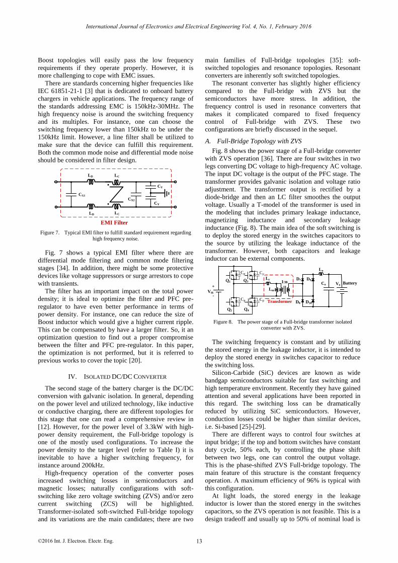
Figure 7. Typical EMI filter to fulfill standard requirement regarding high frequency noise.
Fig. 7 shows a typical EMI filter where there are
differential mode filtering and common mode filtering
stages [34]. In addition, there might be some protective
devices like voltage suppressors or surge arrestors to cope
with transients.
The filter has an important impact on the total power
density; it is ideal to optimize the filter and PFC pre-
regulator to have even better performance in terms of
power density. For instance, one can reduce the size of
Boost inductor which would give a higher current ripple.
This can be compensated by have a larger filter. So, it an
optimization question to find out a proper compromise
between the filter and PFC pre-regulator. In this paper,
the optimization is not performed, but it is referred to
previous works to cover the topic [20].
IV. ISOLATED DC/DC CONVERTER
The second stage of the battery charger is the DC/DC
conversion with galvanic isolation. In general, depending
on the power level and utilized technology, like inductive
or conductive charging, there are different topologies for
this stage that one can read a comprehensive review in
[12]. However, for the power level of 3.3kW with high-
power density requirement, the Full-bridge topology is
one of the mostly used configurations. To increase the
power density to the target level (refer to Table I) it is
inevitable to have a higher switching frequency, for
instance around 200kHz.
High-frequency operation of the converter poses
increased switching losses in semiconductors and
magnetic losses; naturally configurations with soft-
switching like zero voltage switching (ZVS) and/or zero
current switching (ZCS) will be highlighted.
Transformer-isolated soft-switched Full-bridge topology
and its variations are the main candidates; there are two
main families of Full-bridge topologies [35]: soft-
switched topologies and resonance topologies. Resonant
converters are inherently soft switched topologies.
The resonant converter has slightly higher efficiency
compared to the Full-bridge with ZVS but the
semiconductors have more stress. In addition, the
frequency control is used in resonance converters that
makes it complicated compared to fixed frequency
control of Full-bridge with ZVS. These two
configurations are briefly discussed in the sequel.
A. Full-Bridge Topology with ZVS
Fig. 8 shows the power stage of a Full-bridge converter
with ZVS operation [36]. There are four switches in two
legs converting DC voltage to high-frequency AC voltage.
The input DC voltage is the output of the PFC stage. The
transformer provides galvanic isolation and voltage ratio
adjustment. The transformer output is rectified by a
diode-bridge and then an LC filter smoothes the output
voltage. Usually a T-model of the transformer is used in
the modeling that includes primary leakage inductance,
magnetizing inductance and secondary leakage
inductance (Fig. 8). The main idea of the soft switching is
to deploy the stored energy in the switches capacitors to
the source by utilizing the leakage inductance of the
transformer. However, both capacitors and leakage
inductor can be external components.
+
-
Co Vo
Q1
Q2
Q3
Q4
D7
D8
D9
D10
Lo
Vdc
Battery
Lm
Lr
. .
1:n
Transformer
Cp
Cp
Cp
Cp
Figure 8. The power stage of a Full-bridge transformer isolated converter with ZVS.
The switching frequency is constant and by utilizing
the stored energy in the leakage inductor, it is intended to
deploy the stored energy in switches capacitor to reduce
the switching loss.
Silicon-Carbide (SiC) devices are known as wide
bandgap semiconductors suitable for fast switching and
high temperature environment. Recently they have gained
attention and several applications have been reported in
this regard. The switching loss can be dramatically
reduced by utilizing SiC semiconductors. However,
conduction losses could be higher than similar devices,
i.e. Si-based [25]-[29].
There are different ways to control four switches at
input bridge; if the top and bottom switches have constant
duty cycle, 50% each, by controlling the phase shift
between two legs, one can control the output voltage.
This is the phase-shifted ZVS Full-bridge topology. The
main feature of this structure is the constant frequency
operation. A maximum efficiency of 96% is typical with
this configuration.
At light loads, the stored energy in the leakage
inductor is lower than the stored energy in the switches
capacitors, so the ZVS operation is not feasible. This is a
design tradeoff and usually up to 50% of nominal load is
International Journal of Electronics and Electrical Engineering Vol. 4, No. 1, February 2016
©2016 Int. J. Electron. Electr. Eng. 13

selected by the designer. Below this value the converter
efficiency is lower than the nominal condition.
B. Resonant Full-Bridge Topology with LLC
Configuration
Inductor-Inductor-Capacitor (LCC) resonant converter
is one of the attractive alternatives as DC/DC converter
because of high efficiency, high power density, lower
EMI levels and wide operation ranges [37]. The
waveforms are sinusoidal during one or more subinterval
of each switching period [35]; so the small signal
approximation is not valid for the resonance converters.
Fig. 9 shows the power stage of a transformer isolated
LLC resonant converter in which the resonant tank is
specified in the figure. The input bridge provides a square
waveform with a controllable frequency around 80kHz
for example. The resonant tank includes Cr, Lr and Lm
which are a series capacitor, the transformer leakage and
magnetization inductances consequently; the transformer
adjusts the voltage level for the bridge and output low
pass filter. The full analysis of the resonant converter is
not a straightforward task. However, with some
simplifications it is possible to have an acceptable design
procedure. If the main component of the bridge output
voltage is considered, then one can analyze the circuit
based on the phasor method.
+
-
Co Vo
Q1
Q2
Q3
Q4
D7
D8
D9
D10
Lo
Vdc
Battery
Lm
Lr ..1:n
Transformer
Cr
Resonant Tank
Figure 9. The power stage of an isolated Full-bridge LLC resonant converter.
VS1 Lm
LrCr
Req
+
-
Vo/n+ -
Vcr
iLr irect
Vdc
VS1
out
oeq
P
V
nR
2
22
8
Figure 10. Equivalent circuit of the LLC resonant converter considering the fundamental component.
Fig. 10 shows the equivalent circuit diagram of the
LLC converter considering just the first harmonic. The
output rectifier and filter is modeled as an equivalent
resistor [35] considering the transformer turns ratio, n.
The equivalent resistance from the primary side is
out
oeq
P
V
nR
2
22
8
, where Vo and Pout are the output voltage
and power respectively.
By controlling the bridge frequency, the resonant tank
shows different impedances, which is the mechanism to
regulate the output voltage. However, the frequency
variation can’t be extremely wide in order to violate the
first harmonic assumption. The next harmonic of the
bridge square wave is the third one. The variable
frequency control is apparently a negative point
compared to the fixed switching frequency controlled
schemes, especially when it comes to digital
implementation.
As is mentioned earlier, the output battery voltage has
a wide range that can be from 275-400V which makes it
challenging to design the controller especially
considering ZVS or ZCS operation. The best efficiency of
98% [37] is reported for this circuit and it turns out that it
is a viable option for battery charging. At lighter load the
ZVS is not performed that reduces the efficiency of the
charger [37].
V. PRACTICAL EXAMPLE OF THE ONBOARD BATTERY
CHARGER USED IN VOLVO CAR V60
The Norway-based Eltek Company supplied onboard
battery chargers to Volvo Car Corporation to be used in
the V60 PHEV. The charger is a water cooled device
installed in an aluminum enclosure. The CAN controller
in the charger unit provides the communication protocol.
The charger is installed in two different mechanical
enclosures: one with ingress protection (IP) 20 and
another one with IP 67. The device with IP 20 weights
2.8kg and the one with IP 67 weights 4.3kg. The power
density in the first case is 1.8kW/liter, which is very high.
Table II provides a summary of the charger specification.
TABLE II. SPECIFICATIONS OF THE ELTEK 3KW CHARGER [38]
Parameter Value
Input voltage from grid utility
(single-phase) 85-275 V
Maximum value of input current
from the grid 14 A
Ac line frequency range 45-65 Hz
Power factor More than 99%
Total harmonics distortion (THD) Less than 5%
Output dc voltage 250-420 V
Output dc voltage ripple Less than 2 V
Maximum output dc current 10 A
Maximum output power 3 kW
Charger efficiency 96% at 50% load
95% at 100% load
Applicable standards
Electrical safety
EMC: immunity, light industry EMC: immunity, industry
EMC: emission, light industry
EMC: emission, industry
Mains Harmonics
IEC 61851-1
EN 61000-6-1
EN 61000-6-2
EN 61000-6-3 EN 61000-6-4
EN 61000-3-2
Cooling Liquid
Operating temperature -40 to +60 oC
Dimensions 49x280x120mm (IP20) 60x355x167mm (IP67)
Weight 2.8 kg (IP20)
4.3 kg (IP67)
International Journal of Electronics and Electrical Engineering Vol. 4, No. 1, February 2016
©2016 Int. J. Electron. Electr. Eng. 14

VI. CONCLUSIONS
3.3kW battery chargers are a favorable alternative by
auto industries for PHEVs. Different requirements of
such a charger like power density and efficiency are
explained in this paper. The charger has two converter
stages: an AC/DC pre-regulator stage and an isolated
DC/DC converter. Interleaved Boost converter is a
potential topology for the pre-regulator stage. The ZVS
Full-bridge topology and the LLC resonant topology are
the main candidates for the DC/DC stage.
ACKNOWLEDGMENT
The financial support given by Energimyndigheten
(Swedish Energy Agency) is gratefully acknowledged.
REFERENCES
[1] S. Haghbin, “Integrated motor drives and battery chargers for
electric or plug-in hybrid electric vehicles,” PhD thesis, Chalmers
University of Technology, Sweden, 2013. [2] Limits for Harmonic Current Emissions (Equipment Input Current
<16A per Phase), IEC61000-3-2, Aug. 1995.
[3] Electric Vehicle Conductive Charging System - Part 21-1 Electric Vehicle Onboard Charger EMC Requirements for Conductive
Connection to a.c./d.c. Supply, IEC 61851-21-1, 2013.
[4] Electromagnetic Compatibility Series, IEC 61000-4. [5] S. Basu, M. H. J. Bollen, and T. M. Undeland, “PFC Strategies in
light of EN 61000-3-2,” APEC Paper A, 2005.
[6] A. Di Napoli and A. Ndokaj, “EMC and safety in vehicle drives,” in Proc. 14th European Conference on Power Electronics and
Applications (EPE 2011), 2011, pp. 1-8.
[7] J. Muhlethaler, H. Uemura, and J. W. Kolar, “Optimal design of EMI filters for single-phase boost PFC circuits,” in Proc. 38th
Annual Conference on IEEE Industrial Electronics Society, Oct.
2012, pp. 632-638. [8] F. Yang, X. Ruan, Q. Ji, and Z. Ye, “Input differential-mode EMI
of CRM boost PFC converter,” IEEE Transactions on Power
Electronics, vol. 28, no. 3, pp. 1177-1188, Mar. 2013. [9] J. C. Crebier and J. Ferrieux, “PFC full bridge rectifiers EMI
modeling and analysis-common mode disturbance reduction,” IEEE Transactions on Power Electronics, vol. 19, no. 2, pp. 378-
387, Mar. 2004.
[10] M. C. Kya, “Design, implementation, and control of a two stage AC/DC isolated power supply with high input power factor and
high efficiency,” PhD thesis, Middle East Technical University,
2013. [11] K.-W. Koo, D.-H. Kim, D.-G. Woo, and B.-K. Lee, “Topology
and selection guideline,” in Proc. IEEE Vehicle Power and Propulsion Conference (VPPC), Oct. 2012, pp. 1520-1524.
[12] A. Khaligh and S. Dusmez, “Comprehensive topological analysis
of conductive and inductive charging solutions for plug-in electric vehicles,” IEEE Transactions on Vehicular Technology, vol. 61,
no. 8, pp. 3475-3489, Oct. 2012.
[13] D. S. Gautam, F. Musavi, M. Edington, W. Eberle, and W. G. Dunford, “An automotive onboard 3.3-kW battery charger for
PHEV application,” IEEE Transactions on Vehicular Technology,
vol. 61, no. 8, pp. 3466-3474, Oct. 2012. [14] Power Electronics Group, California Institute of Technology,
“Input-Current shaped ac-to-dc converters,” NASA Report
Number N86-25693, May 1986. [15] H. Y. Kanaan, G. Sauriol, and K. Al-Haddad, “Small-Signal
modelling and linear control of a high efficiency dual boost single-
phase power factor correction circuit,” IET Power Electronics, vol. 2, no. 6, pp. 665-674, Nov. 2009.
[16] J. B. Williams, “Design of feedback loop in unity power factor AC
to DC converter,” in Proc. 20th Annual IEEE Power Electronics Specialists Conference, Jun. 1989, pp. 959-967.
[17] R. D. Middlebrook, “Small-Signal modeling of pulse-width
modulated switched-mode power converters,” Proceedings of the IEEE, vol. 76, no. 4, pp. 343-354, Apr. 1988.
[18] P. Cooke, “Modeling average current mode control [of power convertors],” in Proc. Fifteenth Annual IEEE Applied Power
Electronics Conference and Exposition, 2000, pp. 256-262.
[19] W. Tang, F.C. Lee, and R. B. Ridley, “Small-Signal modeling of average current-mode control,” IEEE Transactions on Power
Electronics, vol. 8, no. 2, pp. 112-119, Apr. 1993.
[20] F. A. Huliehel, F. C. Lee, and B. H. Cho, “Small-Signal modeling of the single-phase boost high power factor converter with
constant frequency control,” in Proc. 23rd Annual IEEE Power
Electronics Specialists Conference, 1992, pp. 475-482. [21] R. D. Middlebrook, “Topics in multiple-loop regulators and
current-mode programming,” IEEE Transactions on Power
Electronics, vol. PE-2, no. 2, pp. 109-124, Apr. 1987. [22] L. H. Dixon, “Average current mode control of switching power
supplies,” Unitrode Application Note, 1990.
[23] K. Raggl, T. Nussbaumer, G. Doerig, J. Biela, and J. W. Kolar, “Comprehensive design and optimization of a high-power-density
single-phase boost PFC,” IEEE Transactions on Industrial
Electronics, vol. 56, no. 7, pp. 2574-2587, Jul. 2009. [24] T. Nussbaumer, K. Raggl, and J. W. Kolar, “Design guidelines for
interleaved single-phase boost PFC circuits,” IEEE Transactions
on Industrial Electronics, vol. 56, no. 7, pp. 2559-2573, Jul. 2009. [25] H. Kragh, F. Blaabjerg, and J. K. Pedersen, “An advanced tool for
optimised design of power electronic circuits,” in Proc. Thirty-
Third IAS Annual Meeting, Industry Applications Conference, Oct. 1998, pp. 991-998.
[26] I. K. Budihardjo, Peter O. Lauritzen, and H. A. Mantooth,
“Performance requirements for power MOSFET models,” IEEE Transactions on Power Electronics, vol. 12, no. 1, pp. 36-45, Jan.
1997.
[27] C. L. Ma and P. O. Lauritzen, “A simple power diode model with forward and reverse recovery,” IEEE Transactions on Power
Electronics, vol. 8, no. 4, pp. 342-346, Oct. 1993.
[28] Z. Wang, A. T. Bryant, J. Wu, and P. R. Palmer, “Implementation and comparison of power diode models for system simulation,” in
Proc. International Conference on Power Electronics and Drives
Systems, 2005, vol. 1, pp. 694-699. [29] C. M. Tan and K.-J. Tseng, “Using power diode models for circuit
simulations-a comprehensive review,” IEEE Transactions on Industrial Electronics, vol. 46, no. 3, pp. 637-645, Jun. 1999.
[30] F. Musavi, W. Eberle, and W. G. Dunford, “A high-performance
single-phase bridgeless interleaved PFC converter for plug-in hybrid electric vehicle battery chargers,” IEEE Transactions on
Industry Applications, vol. 47, no. 4, pp. 1833-1843, 2011.
[31] F. Musavi, W. Eberle, and W. G. Dunford, “A phase-shifted gating technique with simplified current sensing for the semi-
bridgeless AC-DC converter,” IEEE Transactions on Vehicular
Technology, vol. 62, no. 4, pp. 1568-1576, May 2013. [32] F. Musavi, D. S. Gautam, W. Eberle, and W. G. Dunford, “A
simplified power loss calculation method for PFC boost
topologies,” in Proc. IEEE Transportation Electrification Conference and Expo (ITEC), Jun. 2013, pp. 1-5.
[33] F. Musavi, W. Eberle, and W. G. Dunford, “Efficiency evaluation
of single-phase solutions for AC-DC PFC boost converters for plug-in-hybrid electric vehicle battery chargers,” in Proc. IEEE
Vehicle Power and Propulsion Conference (VPPC), Sep. 2010, pp.
1-6. [34] M. Pieniz, J. R. Pinheiro, and H. L. Hey, “An investigation of the
boost inductor volume applied to PFC converters,” in Proc. 37th
IEEE Power Electronics Specialists Conference, 2006, pp. 1-7. [35] R. W. Erickson and D. Maksimovic, Fundamentals of Power
Electronics, 2nd ed., Springer, 2001.
[36] D. Gautam, F. Musavi, M. Edington, W. Eberle, and W. Dunford, “A zero voltage switching full-bridge DC-DC converter for an on-
board PHEV battery charger,” in Proc. IEEE Transportation
Electrification Conference and Expo (ITEC), 2012, pp. 1-6. [37] J. Deng, S. Li, S. Hu, C. C. Mi, and R. Ma, “Design methodology
of LLC resonant converters for electric vehicle battery chargers,”
IEEE Trans. on Vehicular Technology, vol. 63, no. 4, May 2014. [38] 3kW Traction Battery Charger Module, Datasheet, Eltek Valere
Co.
Saeid Haghbin received his Master degree in electrical engineering
from Sharif University of Technology, Iran, in 2003. During 2003-2007
he was working in industry mainly on power electronic systems and automation. He received his PhD degree in Electric Power Engineering
International Journal of Electronics and Electrical Engineering Vol. 4, No. 1, February 2016
©2016 Int. J. Electron. Electr. Eng. 15
comparison for 6.6kW on board charger: Performance, efficiency,

in 2013 from Chalmers University of Technology, Sweden. At the present time he is a postdoctoral fellow at Chalmers University of
Technology. His main research interests are power electronics, drive
systems and related signal processing.
Torbjörn Thiringer works at Chalmers university of Technology, in
Gothenburg Sweden, as a professor in applied power electronics. He took his M.Sc and Ph.D at Chalmers University of technology in 1989
and 1996 respectively. His areas of interest include the modeling,
control and grid integration of wind energy converters into power grids as well as power electronics and drives for other types of applications,
such as electrified vehicles, buildings and industrial applications.
International Journal of Electronics and Electrical Engineering Vol. 4, No. 1, February 2016
©2016 Int. J. Electron. Electr. Eng. 16