Embed Size (px)
Citation preview

915-MHz Wireless 64-Channel Neural RecordingSoC with Programmable Mixed-Signal FIR Filters
Karim Abdelhalim and Roman GenovElectrical and Computer Engineering, University of Toronto; Email: {karim, roman}@eecg.utoronto.ca
Abstract— A system-on-chip (SoC) neural recording interfacewith 64 channels, 64 16-tap programmable mixed-signal FIRfilters and a fully integrated 915MHz OOK/FSK closed-loopwireless transmitter is presented. Each recording channel hasa fully differential amplifier with 54dB of gain and utilizes atunable low-distortion subthreshold MOS-resistor to reject DCoffsets with an input-referred noise of 6.5µV and a CMRR of78dB. Each channel contains a modified 8-bit SAR ADC with anENOB of 7.8-bits and can provide analog-digital multiplicationby modifying the the sampling phase of the ADC. It is used inconjunction with 12-bit digital adders and registers to implement64 programmable transposed FIR filters that enable preciseseparation of various bands in the neural spectrum. The 915MHzFSK/OOK transmitter offers data rates up to 1.5Mbps with amaximum output power of 0dBm. The 4x3mm chip fabricated ina 0.13µm CMOS process dissipates 5.03mW from a 1.2V supply.
I. INTRODUCTION
Monitoring neuro-electrical activity in the brain is a vitalmethod in diagnostics and evaluation of various neurologicaldisorders. A number of non-invasive techniques can be usedfor brain function testing such as EEG, MEG, fMRI andPET scans. These methods are complementary and often havelimited efficacy and applicability. Cortical surface electricalrecordings known as electrocorticography (ECoG) providebetter signal-to-noise ratio than scalp surface EEG, as wellas a higher bandwidth, up to 500Hz of signal content, andincreased spatial resolution. 64-site ECoG is currently the goldstandard procedure for seizure localization in most patientswith intractable epilepsy who are candidates for resectivesurgery. Other invasive methods include neural recording frommicroelectrodes, such as Utah electrode arrays employed inexperimental animal and human studies, which allow forrecording signals with even wider bandwidths and for monitor-ing action potentials of individual neurons. Currently most ofthese methods involve tethered wires connecting the electrodesto bench-top neural amplifiers.
An implanted RF wireless interface enables the freedomof movement for a patient, reduces artifacts and noise in therecording data and reduces the possibility of an infection.The requirements of a large number of recording channelsand wide signal bandwidth translate to a high output datarate (>1Mbps). Tissue heating and available power budgetseverely limit the transmitter output power. Existing designsovercome this limitation by transmitting only neural spikeson most or all channels [1], [2] and by utilizing simple low-power transmitter architectures [1], [3]. Spike detection resultsin a loss of vital information such as neural oscillations in the
64
16-TAP FIR FILTER
SHIFT REGISTERCOEFFICIENT
AMP
VV
CONTROLLER
CLKs
14.33MHz CLOCK
1.2V
ANALOGFRONTEND
MIXED-SIGNAL
ON-CHIP
915MHz PLLFSK/OOK
TX
IN0
IN64
SIGNALPROCESSING
REF
VFig. 1. Simplified system diagram of the wireless neural recording SoC.
gamma band present in patients with epilepsy, schizophrenia,Alzheimer’s disease and many other neurological disorders.Simple transmitter architectures have shortcomings and aretypically not fully integrated. Open-loop VCO designs [1],[3] suffer from temperature sensitivity and frequency drift.Basic UWB architectures [4] are susceptible to interferenceand noise.
We present an integrated 64-channel neural recording inter-face system-on-chip (SoC) that densely integrates 64 neuralrecording amplifiers and ADCs, 64 programmable 16-tap FIRfilters, an on-chip digital controller and a fully-integratedclosed-loop wireless transmitter on a 4mm×3mm 0.13µmCMOS die. It performs versatile signal filtering individuallyconfigurable for each channel to extract information of interestsuch as beta, gamma or other frequency bands, local-fieldpotentials (LFP) and spikes. It also performs interferencesuppression, spike detection, precise bandwidth control anda variety of other filtering tasks. A mixed-signal FIR filterimplementation eliminates the need for 512 conventional 8-bitdigital multipliers by efficiently implementing the multiplica-tion within an ADC conversion cycle. This results in over anorder of magnitude savings in the power-area product.
II. SYSTEM ARCHITECTURE AND VLSI IMPLEMENTATION
The full system architecture is shown in Figure 1. It consistsof 64 neural recording amplifiers with a tunable high-passpole frequency in the sub-Hz range. Each channel containsa programmable mixed-signal 16-tap FIR filter. Digital data issent to the 915MHz PLL-based transmitter and modulated us-ing either Manchester encoded FSK or OOK. The transmitteroutput power, FSK modulation index, VCO center frequency
978-1-4577-0704-9/10/$26.00 ©2011 IEEE 223
−
+
RST
RST
C1=11.7pFC2=300fF
C2=300fF
C =3.1pF
C =3.1pF
−
+FOLDED 2-STAGECASCODE
C4=100fF
VDD=1.2VI
VCM=0.6V
VV V
I
C3=1.4pF
C4=100fF
THICK OXIDE
RE
FIN
L
L
HP HP
OU
T
C1=11.7pF
Fig. 2. Schematic of the analog front end.
and the PLL bandwidth can all be programmed. A single off-chip 14.32-MHz crystal oscillator generates all on-chip clocks.
A. Analog Front End
The schematic of the analog front end is shown in Figure2. Amplification and filtering are performed over two stageswith 54dB of gain set by the input and feedback capacitorratios. The first stage uses a fully differential architectureto ensure high CMRR, which is important for dense SoCimplementations. The first stage uses a folded-cascode OTAwith a total current of 3µA. Large PMOS input devices wereselected to minimize flicker noise and are biased in weakinversion to maximize their transconductance. The first stagehas a small output swing and uses two thick oxide NMOSpseudo-resistors as feedback elements which along with C2
yields a high-pass pole in the sub-Hertz region. To maximizeoutput swing, the second stage uses a 2-stage OTA with a totalcurrent of 1µA. The pseudoresistor as implemented in the firststage exhibits distortion as it is a non-linear resistance whenlarge output swings are present [1]. It can be made tuneableby setting its gate to a voltage [5] and operating the device insubthreshold. Setting the VGS of the feedback device too lowleads to leakage issues and bias drifts often saturating the OTA.To address these issues, the feedback resistor in the secondstage was implemented using two source followers to ensurea constant VGS on the subthreshold device for large outputswings as shown in Figure 2. A 10-15dB improvement indistortion at sub-Hz frequencies was observed experimentallywhen using the implemented approach in Figure 2 over theconventional subthreshold transistor when used in the secondstage.
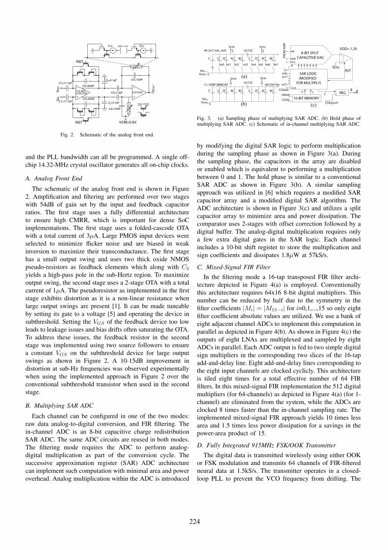
B. Multiplying SAR ADC
Each channel can be configured in one of the two modes:raw data analog-to-digital conversion, and FIR filtering. Thein-channel ADC is an 8-bit capacitive charge redistributionSAR ADC. The same ADC circuits are reused in both modes.The filtering mode requires the ADC to perform analog-digital multiplication as part of the conversion cycle. Thesuccessive approximation register (SAR) ADC architecturecan implement such computation with minimal area and poweroverhead. Analog multiplication within the ADC is introduced
10-BIT MEMORY
8 2
m0m1
m7
Vcm
VIN
VREFVcm
FRO
M A
MP
datain
CLKin
CLK
8
CLKsynch
REG8
Mx
RSTS SAR LOGIC (MODIFIED FOR MULTIPLY)
VDD= 1.2V
C=100fF MIMCAP
−
+
C C 2C 2CC4C 4C8C
16/15CVcm Vcm
Vin
C C 2C 2CC4C 4C8C 8C
16/15CVcm
SVcm
S
Vcm
Sm0 m1 m2 m3 m4 m5 m6 m7
(a)-M/256*Vin
(b) (c)
CLKadc
M={m7,m6...m0}
VinVcm
8-BIT SPLIT CAPACITIVE DAC
S S
8C
SS
Fig. 3. (a) Sampling phase of multiplying SAR ADC. (b) Hold phase ofmultiplying SAR ADC. (c) Schematic of in-channel multiplying SAR ADC.
by modifying the digital SAR logic to perform multiplicationduring the sampling phase as shown in Figure 3(a). Duringthe sampling phase, the capacitors in the array are disabledor enabled which is equivalent to performing a multiplicationbetween 0 and 1. The hold phase is similar to a conventionalSAR ADC as shown in Figure 3(b). A similar samplingapproach was utilized in [6] which requires a modified SARcapacitor array and a modified digital SAR algorithm. TheADC architecture is shown in Figure 3(c) and utilizes a splitcapacitor array to minimize area and power dissipation. Thecomparator uses 2-stages with offset correction followed by adigital buffer. The analog-digital multiplication requires onlya few extra digital gates in the SAR logic. Each channelincludes a 10-bit shift register to store the multiplication andsign coefficients and dissipates 1.8µW at 57kS/s.
C. Mixed-Signal FIR Filter
In the filtering mode a 16-tap transposed FIR filter archi-tecture depicted in Figure 4(a) is employed. Conventionallythis architecture requires 64x16 8-bit digital multipliers. Thisnumber can be reduced by half due to the symmetry in thefilter coefficients |Mi| = |M15−i| for i=0,1,...,15 so only eightfilter coefficient absolute values are utilized. We use a bank ofeight adjacent channel ADCs to implement this computation inparallel as depicted in Figure 4(b). As shown in Figure 4(c) theoutputs of eight LNAs are multiplexed and sampled by eightADCs in parallel. Each ADC output is fed to two simple digitalsign multipliers in the corresponding two slices of the 16-tapadd-and-delay line. Eight add-and-delay lines corresponding tothe eight input channels are clocked cyclicly. This architectureis tiled eight times for a total effective number of 64 FIRfilters. In this mixed-signal FIR implementation the 512 digitalmultipliers (for 64-channels) as depicted in Figure 4(a) (for 1-channel) are eliminated from the system, while the ADCs areclocked 8 times faster than the in-channel sampling rate. Theimplemented mixed-signal FIR approach yields 10 times lessarea and 1.5 times less power dissipation for a savings in thepower-area product of 15.
D. Fully Integrated 915MHz FSK/OOK Transmitter
The digital data is transmitted wirelessly using either OOKor FSK modulation and transmits 64 channels of FIR-filteredneural data at 1.5kS/s. The transmitter operates in a closed-loop PLL to prevent the VCO frequency from drifting. The
224

z -1 z -1+ z -1+ +
Din
Dout(a)
LNA0
LNA1
LNA7
SELECT
ANALOG
FRONT END& ADCs
M0
M1
M7
DIGITAL
CLK7 CLK1 CLK0
DOUT7 DOUT1 DOUT0
TO WIRELESS
V
V
V
V
(c)
IN0
IN1
IN7
REF
CLK_FIR
SELECT
sign15 M0
sign0 M0
sign1 M1
sign7 M7
sign8 M8
sign15 M0
sign14 M1
8
sign14 M1 sign1 M1 sign0 M0ADCVin
z -1 z -1+ z -1+ + Dout(b)
sign15 M0 sign14 M1 sign1 M1 sign0 M0
Vin
MULTIPLYING ADC
Fig. 4. (a) Conventional 16-tap transposed FIR structure. (b) Mixed-signal16-tap transposed FIR filter structure. (c) Schematic of implemented mixed-signal 64 16-tap FIR filters.
full wireless transmitter schematic is shown in Figure 5.The voltage-controlled oscillator (VCO) was implementedusing a cross-coupled architecture with a 12.6nH on-chipinductor implemented using a thick copper top-level metal.A large varactor implemented using a P+/N junction diodewas connected to the control voltage of the VCO to lockthe PLL to 916.3MHz. The data is modulated at high bit-rates through Manchester-encoded FSK on the smaller NMOSvaractors. They consist of binary-weighted transistors and have3-bit programming to adjust the FSK modulation index. Thebandwidth of the PLL must be significantly lower than thedata bit-rate to prevent it from being filtered out by the PLL[7]. The loop filter was implemented on-chip and is tunableto achieve different PLL bandwidths. The output of the VCOis buffered and sent to the power amplifier which utilizes a12.6nH on-chip inductor and a capacitive matching network tomatch to a 50-Ohm antenna. The output power has 4-bit digitaltuning and is adjustable from -20dBm to 0dBm through P0 toP3 in Figure 5. For OOK modulation, the PLL is locked tothe carrier frequency and the cascode transistors of the poweramplifier are turned ON or OFF.
III. EXPERIMENTAL RESULTS
The experimentally measured amplitude frequency responseand input referred noise of a neural recording channel areshown in Figure 6(a) and Figure 6(b), respectively. The high-pass corner frequency can be adjusted from approximately0.1Hz to 10Hz by adjusting the bias current of the sourcefollower in Figure 2. Integrating the noise over the bandwidth
MANCHESTERDATA
FSK DATA
STATIC CMOS
14.3
2MH
z
750uA
5.1pF
92pF75k
Icp=10 A
−
+
P3 P2 P1 P0
Vgate
BONDPAD
ANTENNA
12.6nH 2.9pF
4pF
160k
25.6pF−
+
12.6nH
ENCODER
OOKMODULATOR
P0- P
3
3.1pF3.1pF
PHA
SE
DET
ECTO
RC
HA
RGE
PUM
PA
ND
Vctl
FREQ
UEN
CY
Ω
Ω
μ
DIVIDER /64
M0,M1M2,M3
M4,M5
M6M7M8M9
15x2 m/120nmμ45x2 m/120nmμ
3-T BINARY WEIGHTEDμ
40x2 m/120nmμ20x2 m/120nmμ10x2 m/120nmμ 6x2 m/120nmμ
DEVICE SIZE
M2,M3
M0,M1
M4 M5
M6 M7 M8 M9
BANK 2,4,8x2.5 m/120nm
Fig. 5. Schematic of the wireless transmitter.
0 200 400 600 800 1000 1200 1400 1600 1800−40
−20
0
MA
G (d
B)
0 200 400 600 800 1000 1200 1400 1600 1800
−40
−20
0
MA
G (d
B)
0 200 400 600 800 1000 1200 1400 1600 1800
−40
−20
0
MA
G (d
B)
0 200 400 600 800 1000 1200 1400 1600 1800
−40
−20
0
INPUT FREQUENCY (Hz)
MA
G (d
B)
MEASUREDIDEAL
MEASUREDIDEAL
MEASUREDIDEAL
MEASUREDIDEAL
5000 10000 15000 20000 250000
−100
−80
−60
−40
−20
0
MA
G (d
B)
0 5000 10000 15000 20000 250000
2
4
6
8
10
1
3
5
7
9
INPUT FREQUENCY (Hz)
ENO
B (B
ITS)
INPUT FREQUENCY=1kHzSAMPLE RATE=56kS/s
ENOB=7.8 bits
(c)
(d)
(e)
(f)
(g)
(h)
0.1 1 10 100 1000 1000035
40
45
50
55
(a)
MA
G (d
B)
0.1 100 1000 10000101
1
100
10
0.01
0.1
(b)INPU
T RE
FERR
ED N
OIS
E (
V rm
s/sq
rt(H
z))
Ihp=60nAIhp=150nAIhp=300nA
INTEGRATED NOISE FROM 10Hz to 5kHz is 6.5µVrmsµ
Fig. 6. (a)(b) Measured amplitude response and input-referred noise of theanalog front end. (c) FFT of an in-channel ADC output for 1kHz sinusoidinput at 54kS/s (d) ENOB vs. input frequency for an in-channel ADC. (e)-(h)Measured filter responses of different FIR filters at 7.1kSps.
of 10Hz to 5kHz results in an input-referred noise of 6.5µVrms
and an NEF of 7.2. The CMRR at 1kHz is 78dB.The experimentally measured ADC performance is shown
in Figure 6(c) and (d) with an ENOB of 7.8 and close to 7-bitsover the full Nyquist bandwidth when sampled at 54kS/s. Fourdifferent 16-tap FIR configurations operating at 7.1kS/s (twodifferent low-pass, one high-pass, and one band-pass filter) areshown in Figure 6(e) to (h) with a very close match betweenthe experimental result and the ideal filter response.
Experimental results for the wireless transmitter are shownin Figure 7. Figure 7(a) shows the spectrum analyzer with1.2Mbps of Manchester-encoded FSK data and Figure 7(b)shows transmitted and received data at a distance of 1m.Figure 7(c) shows OOK-modulated data on an oscilloscopeand Figure 7(d) shows transmitted and received OOK datafrom a distance of 1m. The full transmitter dissipates 3.7mWand 6.6mW in FSK-mode for an output power of -20dBm and0dBm, respectively and 5mW for 0dBm OOK modulation.
Figure 8(a) shows the wireless neural recording SoC im-plemented in a standard 1P8M 0.13µm CMOS technology
225

3 4 5 6 7 8 9 10
0
0.5
1
1.5
(V)
3 4 5 6 7 8 9 10
0
0.2
0.4
0.6
0.8
1
TIME ( µ s)
(V)
’10’=1 ’10’=1 ’10’=1 ’01’=0 ’10’=1 ’10’=1 ’01’=0 ’01’=0 ’10’=1
10kbps OOK RAW MODULATED DATA
OUTPUT OF PA INTO 50-OHM LOAD
RAW TRANSMITTED DATA
RECEIVED OOK-MODULATED DATA
RAW TRANSMITTED DATA AT 1.2Mbps
RECEIVED MANCHESTER FSK DATA
(a) (b)
(c) (d)
MANCHESTER ENCODED RECEIVED DATA AT 1.2Mbps
916.4MHz
Fig. 7. (a) Spectrum of FSK-modulated data at a 1m distance. (b) Transmittedand received data from 1m distance at 1.2Mbps using FSK-modulation.(c) OOK modulated data into 50-ohm termination and (d) transmitted andreceived data from a 1m distance at 10kb/s using OOK modulation.
which occupies 4×3mm2 of area. An array of 8x8 neuralrecording channels are organized on a 300µm pitch grid tobe flip-chip bonded to a 8x8 trace carrier or an electrodearray. The power dissipation of the neural recording SoC is0.8mW for the analog front end, ADCs and biasing, 0.53mWfor the digital controller and the adders/registers to implementthe FIR filters while operating at 7.1kS/s. The total systempower dissipation is 5.03mW from a 1.2V supply when usingFSK modulation with a -20dBm output power. A comparisonwith other wireless neural recording SoCs is given in Table I.
The functionality of the analog front end, ADC and FIRfilters was also verified with pre-recorded neural activity ofepileptic seizure events. Seizure-like events were induced in anintact hippocampus from Wilstar rats by immersing it in a low-Mg2+ solution. The signals were recorded with a conventionalbench-top low-noise amplifier and then programmed onto anarbitrary waveform generator with the original signal as shownin Figure 8(b). The input signal was then contaminated with60Hz interference with a much larger power than that of thepre-recorded signal as shown in Figure 8(c) and applied to oneof the 64 channels on the chip. The FIR filter was programmedwith the bandpass filter response shown in Figure 6(h). Figure8(d) shows the output after the FIR filtering with the neuralactivity clearly visible and the 60Hz interference removed.
IV. CONCLUSION
A 0.13µm CMOS wireless neural recording SoC is pre-sented. The die integrates 64 fully differential recording ampli-fiers with 64 SAR ADCs modified to perform in-channel mul-tiplication. This implements 64 programmable 16-tap mixed-signal FIR filters to perform versatile signal filtering in eachchannel. A fully integrated PLL-based FSK/OOK transmitterwirelessly sends the digitized neural recorded data at up to1.5Mb/s. The total power dissipation is 5.1mW from a 1.2Vsupply.
−1−0.5
0
10.5
−1
0
1
−20
0
20
40
0.4 0.45 0.5 0.55 0.6 0.65
0.4 0.45 0.5 0.55 0.6 0.65
0.4 0.45 0.5 0.55 0.6 0.65
(b)
(c)
(d)
AM
P (m
V)A
MP
(mV)
DIG
ITA
L O
UTP
UT
64 NEURAL RECORDING
AMPLIFIERS &
64 8-BIT SAR ADCs
WITH MULTIPLICATION
32x16 12-BIT ADDERS & REGISTERSFOR FIR FILTERS
32x16 12-BIT ADDERS & REGISTERSFOR FIR FILTERS
CONTROLLER915MHz 915MHz
PLL PA
(a)
Fig. 8. (a) Micrograph of the 4×3mm2 0.13µm CMOS prototype. (b)Original prerecorded neural spike from a rat. (c) The input into the amplifierwhich includes the signal from (b) and an added 60-Hz interference. (d)Output after the amplifier and ADC/FIR filter programmed to implement aBP filter.
TABLE I
INTEGRATED WIRELESS NEURAL RECORDING SOCS.
Spec. [1] [2] [3] [4] THIS WORK
Power Diss. 13.5mW 17.2mW 7.05mW 6.0mW 5.03mWCMOS Tech. 0.5µm 0.35µm 0.5µm 0.35µm 0.13µmArea (mm)2 27.3 8.4 16.3 63.4 12Supply (V) 3.3 3.0 3.0 3.3 1.2
# Rec. Chan. 100 16 32 128 64Power/ch. 38µW 9µW 75µW 11µW 6.3µWGain (dB) 60 60 68-78 57-60 54-60
Noise 5.1µV 3.1µV 9.3µV 4.9µV 6.5µVADC 1xSAR 1xSAR PWM 1xSAR 64xSAR
ADC Res. 9b 8b N/A 6-9b 8bSig. Proc. Spike Spike None Spike 64x16t-FIR
Programmable No No No Yes YesRF Carrier 433MHz 433MHz 915MHz 3.1GHz 915MHzModulation FSK FSK FSK/OOK UWB FSK/OOKData rate 330kb/s 1.25Mb/s 708kS/s 90Mb/s 1.5Mb/s
PLL No Yes No No YesFully Int. TX No No No Yes YesPout(dBm) N/A 0 -22 N/A -20 to 0PDC (mW) 4.0 16.6 3.3 4.8 3.7 to 6.6
REFERENCES
[1] R R. Harrison, P T. Watkins, R J. Kier, R O. Lovejoy, D J. Black, BradleyGreger, and Florian Solzbacher, “A low-power integrated circuit for awireless 100-electrode neural recording system,” IEEE Journal of Solid-State Circuits, vol. 42, no. 1, pp. 123–133, January 2007.
[2] A. Bonfanti, M. Ceravolo, G. Zambra, R. Gusmeroli, T. Borghi,A. Spinelli, and A. Lacaita, “A multi-channel low-power IC for neuralspike recording with data compression and narrowband 400-MHz MC-FSK wireless transmission,” IEEE European Solid-State Circuits Confer-ence, Sept. 2010.
[3] S. Lee, H. Lee, M. Kiani, U. Jow, and M. Ghovanloo, “An inductivelypowered scalable 32-channel wireless neural recording system-on-a-chipfor neuroscience applications,” IEEE International Solid-State CircuitsConference, pp. 120–121, Feb. 2010.
[4] M S Chae, W Liu, Z Yang, T Chen, J Kim, M Sivaprakasam, and M Yuce,“A 128-channel 6mW wireless neural recording IC with on-the-fly spikesorting and UWB transmitter,” IEEE International Solid-State CircuitsConference Digest of Technical Papers, pp. 146–603, February 2008.
[5] J. N. Y. Aziz, K. Abdelhalim, R. Shulyzki, B. L. Bardakjian, M. Der-chansky, D. Serletis, P. L. Carlen, and R. Genov, “256-channel neuralrecording and delta compression microsystem with 3D electrodes,” IEEEJournal of Solid-State Circuits, vol. 44, pp. 995–1005, March 2009.
[6] J. Kang, D. T. Lin, L. Li, and M. P. Flynn, “A reconfigurable FIRfilter embedded in a 9b successive approximately ADC,” IEEE CustomIntegrated Circuits Conference, pp. 711–714, September 2008.
[7] S. Cho and A. P. Chandrakasan, “A 6.5-Ghz energy-efficient BFSKmodulator for wireless sensor applications,” IEEE Journal of Solid-StateCircuits, vol. 39, no. 5, pp. 731–739, May 2004.
226


![PVCPR11 Edital 3.5 GHz v03.ppt [Modo de Compatibilidade]...2011/06/09 · 35 MHz 35 MHz 10 MHz 10 MHz 10 MHz 10 MHz 10 MHz 10 MHz 3.400,00 MHz 3.600,00 MHz 10 MHz 35 MHz 10 MHz 10](https://img.dokumen.tips/doc/110x75/5f7286506e7f433bb4685297/pvcpr11-edital-35-ghz-v03ppt-modo-de-compatibilidade-20110609-35-mhz.jpg)


![arXiv:2005.13949v1 [physics.app-ph] 25 May 20207.5 MHz F4 6.5 MHz F5 F6 7.5 MHz F7 F8 6.5 MHz F14 9.5 MHz F15 NA F16 8.5 MHz F17 NA F18 NA F19 7.5 MHz F11 6.5 MHz F20 NA F21 8.5 MHz](https://img.dokumen.tips/doc/110x75/5f758878eb2d114487007824/arxiv200513949v1-25-may-2020-75-mhz-f4-65-mhz-f5-f6-75-mhz-f7-f8-65-mhz.jpg)