Embed Size (px)
Citation preview
*Other brands and names are the property of their respective owners.Information in this document is provided in connection with Intel products. Intel assumes no liability whatsoever, including infringement of any patent orcopyright, for sale and use of Intel products except as provided in Intel’s Terms and Conditions of Sale for such products. Intel retains the right to makechanges to these specifications at any time, without notice. Microcomputer Products may have minor variations to this specification known as errata.
July, 2004COPYRIGHT © INTEL CORPORATION, 2004 Order Number: 272336-005
8XC52/54/58CHMOS SINGLE-CHIP 8-BIT MICROCONTROLLER
Commercial/Express
87C52/80C52/80C32/87C54/80C54/87C58/80C58*See Table 1 for Proliferation Options
Y High Performance CHMOS EPROM/ROM/CPU
Y 12/24/33 MHz Operations
Y Three 16-Bit Timer/Counters
Y Programmable Clock Out
Y Up/Down Timer/Counter
Y Three Level Program Lock System
Y 8K/16K/32K On-Chip Program Memory
Y 256 Bytes of On-Chip Data RAM
Y Improved Quick Pulse ProgrammingAlgorithm
Y Boolean Processor
Y 32 Programmable I/O Lines
Y 6 Interrupt Sources
Y Programmable Serial Channel with:Ð Framing Error DetectionÐ Automatic Address Recognition
Y TTL and CMOS Compatible LogicLevels
Y 64K External Program Memory Space
Y 64K External Data Memory Space
Y MCSÉ 51 Microcontroller CompatibleInstruction Set
Y Power Saving Idle and Power DownModes
Y ONCE (On-Circuit Emulation) Mode
Y Four-Level Interrupt Priority
Y Extended Temperature Range Exceptfor 33 MHz Offering (b40§C to a85§C)
MEMORY ORGANIZATION
ROM EPROM ROMless ROM/EPROM RAM
Device Version Version Bytes Bytes
80C52 87C52 80C32 8K 256
80C54 87C54 80C32 16K 256
80C58 87C58 80C32 32K 256
These devices can address up to 64 Kbytes of external program/data memory.
The Intel 8XC52/8XC54/8XC58 is a single-chip control-oriented microcontroller which is fabricated on Intel’sreliable CHMOS III-E technology. Being a member of the MCS 51 family of controllers, the 8XC52/8XC54/8XC58 uses the same powerful instruction set, has the same architecture, and is pin-for-pin compatible withthe existing MCS 51 family of products. The 8XC52/8XC54/8XC58 is an enhanced version of the87C51/80C51BH/80C31BH. The added features make it an even more powerful microcontroller for applica-tions that require clock output, and up/down counting capabilities such as motor control. It also has a moreversatile serial channel that facilitates multi-processor communications.
Throughout this document 8XC5X will refer to the 8XC52, 80C32, 8XC54 and 8XC58 unless informationapplies to a specific device.
8XC52/54/58
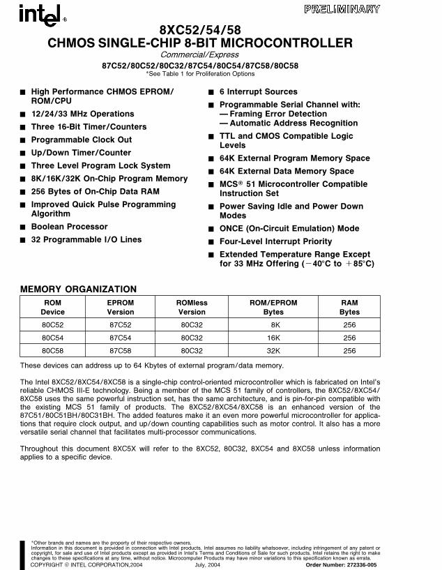
Table 1. Proliferations Options
Standard*1 -1 -2 -24 -33
80C32 X X X X X
80C52 X X X X X
87C52 X X X X X
80C54 X X X X X
87C54 X X X X X
80C58 X X X X X
87C58 X X X X X
NOTES:*1 3.5 MHz to 12 MHz; 5V g20%-1 3.5 MHz to 16 MHz; 5V g20%-2 0.5 MHz to 12 MHz; 5V g20%-24 3.5 MHz to 24 MHz; 5V g20%-33 3.5 MHz to 33 MHz; 5V g10%
272336–1
Figure 1. 8XC5X Block Diagram
2
8XC52/54/58
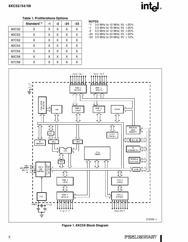
PROCESS INFORMATIONThis device is manufactured on P629.0, a CHMOSIII-E process. Additional process and reliability infor-mation is available in the Intel® Quality SystemHandbook .
PACKAGES40-Pin Plastic DIP (OTP)40-Pin CERDIP (EPROM)44-Pin PLCC (OTP)44-Pin QFP (OTP)
272336–2
DIP
272336–3
PLCC
272336–4
*Do not connect reserved pins. QFP
Figure 2. Pin Connections
3
8XC52/54/58
PIN DESCRIPTIONS
VCC: Supply voltage.
VSS: Circuit ground.
VSS1: Secondary ground (not on DIP). Provided toreduce ground bounce and improve power supplyby-passing.
NOTE:This pin is not a substitute for the VSS pin (pin 22).(Connection not necessary for proper operation.)
Port 0: Port 0 is an 8-bit, open drain, bidirectionalI/O port. As an output port each pin can sink severalLS TTL inputs. Port 0 pins that have 1’s written tothem float, and in that state can be used as high-im-pedance inputs.
Port 0 is also the multiplexed low-order address anddata bus during accesses to external Program andData Memory. In this application it uses strong inter-nal pullups when emitting 1’s, and can source andsink several LS TTL inputs.
Port 0 also receives the code bytes during EPROMprogramming, and outputs the code bytes duringprogram verification. External pullup resistors are re-quired during program verification.
Port 1: Port 1 is an 8-bit bidirectional I/O port withinternal pullups. The Port 1 output buffers can driveLS TTL inputs. Port 1 pins that have 1’s written tothem are pulled high by the internal pullups, and inthat state can be used as inputs. As inputs, Port 1pins that are externally pulled low will source current(IIL, on the data sheet) because of the internal pull-ups.
In addition, Port 1 serves the functions of the follow-ing special features of the 8XC5X:
Port Pin Alternate Function
P1.0 T2 (External Count Input to Timer/Counter 2), Clock-Out
P1.1 T2EX (Timer/Counter 2 Capture/Reload Trigger and Direction Control)
Port 1 receives the low-order address bytes duringEPROM programming and verifying.
Port 2: Port 2 is an 8-bit bidirectional I/O port withinternal pullups. The Port 2 output buffers can driveLS TTL inputs. Port 2 pins that have 1’s written tothem are pulled high by the internal pullups, and inthat state can be used as inputs. As inputs, Port 2
pins that are externally pulled low will source current(IIL, on the data sheet) because of the internal pull-ups.
Port 2 emits the high-order address byte duringfetches from external Program Memory and duringaccesses to external Data Memory that use 16-bitaddresses (MOVX @DPTR). In this application ituses strong internal pullups when emitting 1’s. Dur-ing accesses to external Data Memory that use 8-bitaddresses (MOVX @Ri), Port 2 emits the contents ofthe P2 Special Function Register.
Some Port 2 pins receive the high-order address bitsduring EPROM programming and program verifica-tion.
Port 3: Port 3 is an 8-bit bidirectional I/O port withinternal pullups. The Port 3 output buffers can driveLS TTL inputs. Port 3 pins that have 1’s written tothem are pulled high by the internal pullups, and inthat state can be used as inputs. As inputs, Port 3pins that are externally pulled low will source current(IIL, on the data sheet) because of the pullups.
Port 3 also serves the functions of various specialfeatures of the 8051 Family, as listed below:
Port Pin Alternate Function
P3.0 RXD (serial input port)
P3.1 TXD (serial output port)
P3.2 INT0 (external interrupt 0)
P3.3 INT1 (external interrupt 1)
P3.4 T0 (Timer 0 external input)
P3.5 T1 (Timer 1 external input)
P3.6 WR (external data memory write strobe)
P3.7 RD (external data memory read strobe)
RST: Reset input. A high on this pin for two machinecycles while the oscillator is running resets the de-vice. The port pins will be driven to their reset condi-tion when a minimum VIHI voltage is applied whetherthe oscillator is running or not. An internal pulldownresistor permits a power-on reset with only a capaci-tor connected to VCC.
ALE: Address Latch Enable output pulse for latchingthe low byte of the address during accesses to ex-ternal memory. This pin (ALE/PROG) is also theprogram pulse input during EPROM programming forthe 87C5X.
In normal operation ALE is emitted at a constantrate of (/6 the oscillator frequency, and may be usedfor external timing or clocking purposes. Note, how-ever, that one ALE pulse is skipped during each ac-cess to external Data Memory.
4
8XC52/54/58
If desired, ALE operation can be disabled by settingbit 0 of SFR location 8EH. With this bit set, the pin isweakly pulled high. However, the ALE disable fea-ture will be suspended during a MOVX or MOVC in-struction, idle mode, power down mode and ICEmode. The ALE disable feature will be terminated byreset. When the ALE disable feature is suspended orterminated, the ALE pin will no longer be pulled upweakly. Setting the ALE-disable bit has no affect ifthe microcontroller is in external execution mode.
Throughout the remainder of this data sheet, ALEwill refer to the signal coming out of the ALE/PROGpin, and the pin will be referred to as the ALE/PROGpin.
PSEN: Program Store Enable is the read strobe toexternal Program Memory.
When the 8XC5X is executing code from externalProgram Memory, PSEN is activated twice eachmachine cycle, except that two PSEN activationsare skipped during each access to external DataMemory.
EA/VPP: External Access enable. EA must bestrapped to VSS in order to enable the device tofetch code from external Program Memory locations0000H to 0FFFFH. Note, however, that if any of theLock bits are programmed, EA will be internallylatched on reset.
EA should be strapped to VCC for internal programexecutions.
This pin also receives the programming supply volt-age (VPP) during EPROM programming.
XTAL1: Input to the inverting oscillator amplifier.
XTAL2: Output from the inverting oscillator amplifi-er.
OSCILLATOR CHARACTERISTICS
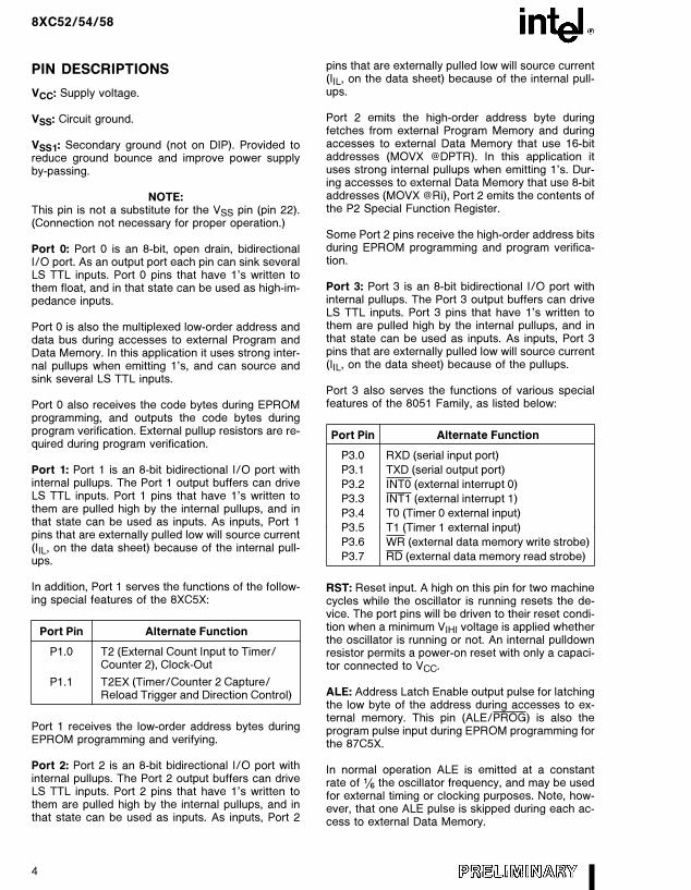
XTAL1 and XTAL2 are the input and output, respec-tively, of a inverting amplifier which can be config-ured for use as an on-chip oscillator, as shown inFigure 3. Either a quartz crystal or ceramic resonatormay be used. More detailed information concerningthe use of the on-chip oscillator is available in Appli-cation Note AP-155, ‘‘Oscillators for Microcontrol-lers’’, Order No. 230659.
272336–5
C1, C2 e 30 pF g10 pF for CrystalsFor Ceramic Resonators, contact resonator manufac-turer.
Figure 3. Oscillator Connections
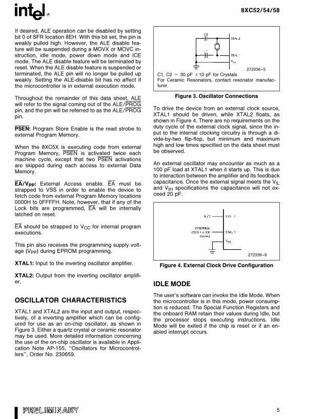
To drive the device from an external clock source,XTAL1 should be driven, while XTAL2 floats, asshown in Figure 4. There are no requirements on theduty cycle of the external clock signal, since the in-put to the internal clocking circuitry is through a di-vide-by-two flip-flop, but minimum and maximumhigh and low times specified on the data sheet mustbe observed.
An external oscillator may encounter as much as a100 pF load at XTAL1 when it starts up. This is dueto interaction between the amplifier and its feedbackcapacitance. Once the external signal meets the VILand VIH specifications the capacitance will not ex-ceed 20 pF.
272336–6
Figure 4. External Clock Drive Configuration
IDLE MODE
The user’s software can invoke the Idle Mode. Whenthe microcontroller is in this mode, power consump-tion is reduced. The Special Function Registers andthe onboard RAM retain their values during Idle, butthe processor stops executing instructions. IdleMode will be exited if the chip is reset or if an en-abled interrupt occurs.
5
8XC52/54/58
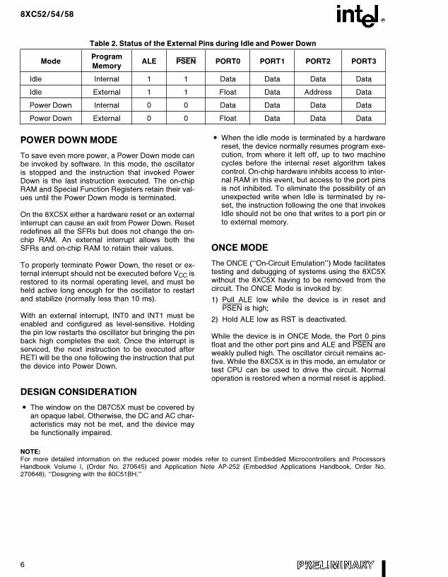
Table 2. Status of the External Pins during Idle and Power Down
ModeProgram
ALE PSEN PORT0 PORT1 PORT2 PORT3Memory
Idle Internal 1 1 Data Data Data Data
Idle External 1 1 Float Data Address Data
Power Down Internal 0 0 Data Data Data Data
Power Down External 0 0 Float Data Data Data
POWER DOWN MODE
To save even more power, a Power Down mode canbe invoked by software. In this mode, the oscillatoris stopped and the instruction that invoked PowerDown is the last instruction executed. The on-chipRAM and Special Function Registers retain their val-ues until the Power Down mode is terminated.
On the 8XC5X either a hardware reset or an externalinterrupt can cause an exit from Power Down. Resetredefines all the SFRs but does not change the on-chip RAM. An external interrupt allows both theSFRs and on-chip RAM to retain their values.
To properly terminate Power Down, the reset or ex-ternal interrupt should not be executed before VCC isrestored to its normal operating level, and must beheld active long enough for the oscillator to restartand stabilize (normally less than 10 ms).
With an external interrupt, INT0 and INT1 must beenabled and configured as level-sensitive. Holdingthe pin low restarts the oscillator but bringing the pinback high completes the exit. Once the interrupt isserviced, the next instruction to be executed afterRETI will be the one following the instruction that putthe device into Power Down.
DESIGN CONSIDERATION
# The window on the D87C5X must be covered byan opaque label. Otherwise, the DC and AC char-acteristics may not be met, and the device maybe functionally impaired.
# When the idle mode is terminated by a hardwarereset, the device normally resumes program exe-cution, from where it left off, up to two machinecycles before the internal reset algorithm takescontrol. On-chip hardware inhibits access to inter-nal RAM in this event, but access to the port pinsis not inhibited. To eliminate the possibility of anunexpected write when Idle is terminated by re-set, the instruction following the one that invokesIdle should not be one that writes to a port pin orto external memory.
ONCE MODE
The ONCE (‘‘On-Circuit Emulation’’) Mode facilitatestesting and debugging of systems using the 8XC5Xwithout the 8XC5X having to be removed from thecircuit. The ONCE Mode is invoked by:
1) Pull ALE low while the device is in reset andPSEN is high;
2) Hold ALE low as RST is deactivated.
While the device is in ONCE Mode, the Port 0 pinsfloat and the other port pins and ALE and PSEN areweakly pulled high. The oscillator circuit remains ac-tive. While the 8XC5X is in this mode, an emulator ortest CPU can be used to drive the circuit. Normaloperation is restored when a normal reset is applied.
NOTE:For more detailed information on the reduced power modes refer to current Embedded Microcontrollers and ProcessorsHandbook Volume I, (Order No. 270645) and Application Note AP-252 (Embedded Applications Handbook, Order No.270648), ‘‘Designing with the 80C51BH.’’
6
8XC52/54/58
8XC5X EXPRESSThe Intel EXPRESS system offers enhancements tothe operational specifications of the MCS 51 familyof microcontrollers. These EXPRESS products aredesigned to meet the needs of those applicationswhose operating requirements exceed commercialstandards.
The EXPRESS program includes the commercialstandard temperature range with burn-in and an ex-tended temperature range with or without burn-in.
With the commercial standard temperature range,operational characteristics are guaranteed over thetemperature range of 0°C to a 70°C. With the ex-tended temperature range option, operational char-acteristics are guaranteed over the range of -40°Cto +85°C.
The optional burn-in is dynamic for a minimum timeof 168 hours at 125°C with VCC = 6.9V ± 0.25V,following guidelines in MIL-STD-883, Method 1015.
For the extended temperature range option, thisdata sheet specifies the parameters which deviatefrom their commercial temperature range limits.
NOTE:Intel offers Express Temperature specifica-tions for all 8XC5X speed options except for33 MHz.
7
8XC52/54/58
ABSOLUTE MAXIMUM RATINGS*
Ambient Temperature Under Bias Àb40§C to a85§CStorage Temperature ÀÀÀÀÀÀÀÀÀÀb65§C to a150§CVoltage on EA/VPP Pin to VSS ÀÀÀÀÀÀÀ0V to a13.0V
Voltage on Any Other Pin to VSS ÀÀb0.5V to a6.5V
IOL Per I/O Pin ÀÀÀÀÀÀÀÀÀÀÀÀÀÀÀÀÀÀÀÀÀÀÀÀÀÀÀ15 mA
Power DissipationÀÀÀÀÀÀÀÀÀÀÀÀÀÀÀÀÀÀÀÀÀÀÀÀÀÀ1.5W(based on PACKAGE heat transfer limitations, notdevice power consumption)
NOTICE: This data sheet contains preliminary infor-mation on new products in production. The specifica-tions are subject to change without notice. Verify withyour local Intel Sales office that you have the latestdata sheet before finalizing a design.
*WARNING: Stressing the device beyond the ‘‘AbsoluteMaximum Ratings’’ may cause permanent damage.These are stress ratings only. Operation beyond the‘‘Operating Conditions’’ is not recommended and ex-tended exposure beyond the ‘‘Operating Conditions’’may affect device reliability.
OPERATING CONDITIONS
Symbol Description Min Max Units
TA Ambient Temperature Under Bias
Commercial 0 a70 §CExpress b40 a85 §C
VCC Supply Voltage 4.0 6.0 V
8XC5X-33 4.5 5.5 V
fOSC Oscillator Frequency
8XC5X 3.5 12 MHz
8XC5X-1 3.5 16 MHz
8XC5X-2 0.5 12 MHz
8XC5X-24 3.5 24 MHz
8XC5X-33 3.5 33 MHz
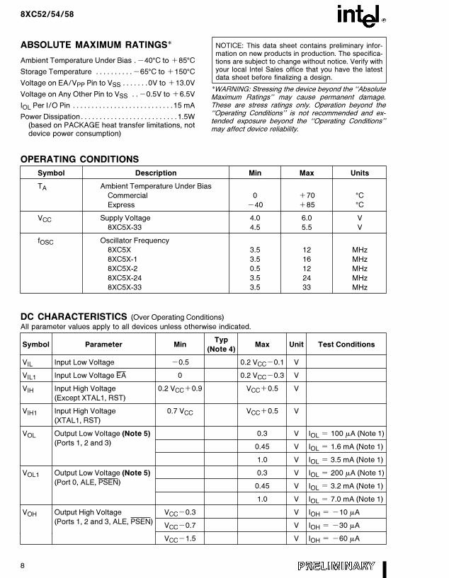
DC CHARACTERISTICS (Over Operating Conditions)
All parameter values apply to all devices unless otherwise indicated.
Symbol Parameter MinTyp
Max Unit Test Conditions(Note 4)
VIL Input Low Voltage b0.5 0.2 VCCb0.1 V
VIL1 Input Low Voltage EA 0 0.2 VCCb0.3 V
VIH Input High Voltage 0.2 VCCa0.9 VCCa0.5 V
(Except XTAL1, RST)
VIH1 Input High Voltage 0.7 VCC VCCa0.5 V
(XTAL1, RST)
VOL Output Low Voltage (Note 5) 0.3 V IOL e 100 mA (Note 1)
(Ports 1, 2 and 3)0.45 V IOL e 1.6 mA (Note 1)
1.0 V IOL e 3.5 mA (Note 1)
VOL1 Output Low Voltage (Note 5) 0.3 V IOL e 200 mA (Note 1)
(Port 0, ALE, PSEN)0.45 V IOL e 3.2 mA (Note 1)
1.0 V IOL e 7.0 mA (Note 1)
VOH Output High Voltage VCCb0.3 V IOH e b10 mA
(Ports 1, 2 and 3, ALE, PSEN)VCCb0.7 V IOH e b30 mA
VCCb1.5 V IOH e b60 mA
8
8XC52/54/58
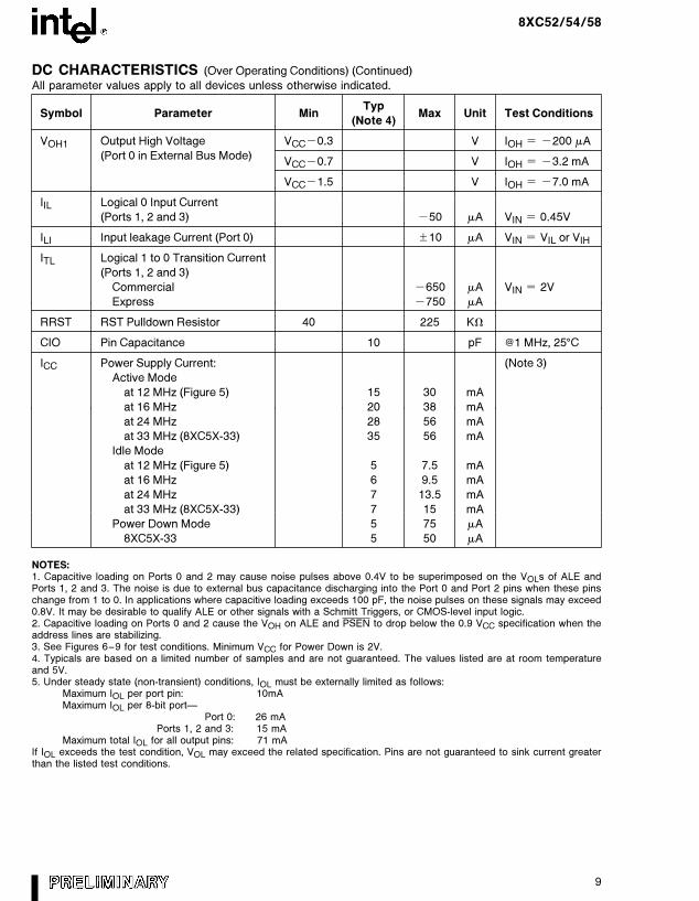
DC CHARACTERISTICS (Over Operating Conditions) (Continued)
All parameter values apply to all devices unless otherwise indicated.
Symbol Parameter MinTyp
Max Unit Test Conditions(Note 4)
VOH1 Output High Voltage VCCb0.3 V IOH e b200 mA
(Port 0 in External Bus Mode)VCCb0.7 V IOH e b3.2 mA
VCCb1.5 V IOH e b7.0 mA
IIL Logical 0 Input Current
(Ports 1, 2 and 3) b50 mA VIN e 0.45V
ILI Input leakage Current (Port 0) g10 mA VIN e VIL or VIH
ITL Logical 1 to 0 Transition Current
(Ports 1, 2 and 3)
Commercial b650 mA VIN e 2V
Express b750 mA
RRST RST Pulldown Resistor 40 225 KX
CIO Pin Capacitance 10 pF @1 MHz, 25§CICC Power Supply Current: (Note 3)
Active Mode
at 12 MHz (Figure 5) 15 30 mA
at 16 MHz 20 38 mA
at 24 MHz 28 56 mA
at 33 MHz (8XC5X-33) 35 56 mA
Idle Mode
at 12 MHz (Figure 5) 5 7.5 mA
at 16 MHz 6 9.5 mA
at 24 MHz 7 13.5 mA
at 33 MHz (8XC5X-33) 7 15 mA
Power Down Mode 5 75 mA
8XC5X-33 5 50 mA
NOTES:1. Capacitive loading on Ports 0 and 2 may cause noise pulses above 0.4V to be superimposed on the VOLs of ALE andPorts 1, 2 and 3. The noise is due to external bus capacitance discharging into the Port 0 and Port 2 pins when these pinschange from 1 to 0. In applications where capacitive loading exceeds 100 pF, the noise pulses on these signals may exceed0.8V. It may be desirable to qualify ALE or other signals with a Schmitt Triggers, or CMOS-level input logic.2. Capacitive loading on Ports 0 and 2 cause the VOH on ALE and PSEN to drop below the 0.9 VCC specification when theaddress lines are stabilizing.3. See Figures 6–9 for test conditions. Minimum VCC for Power Down is 2V.4. Typicals are based on a limited number of samples and are not guaranteed. The values listed are at room temperatureand 5V.5. Under steady state (non-transient) conditions, IOL must be externally limited as follows:
Maximum IOL per port pin: 10mAMaximum IOL per 8-bit portÐ
Port 0: 26 mAPorts 1, 2 and 3: 15 mA
Maximum total IOL for all output pins: 71 mAIf IOL exceeds the test condition, VOL may exceed the related specification. Pins are not guaranteed to sink current greaterthan the listed test conditions.
9
8XC52/54/58
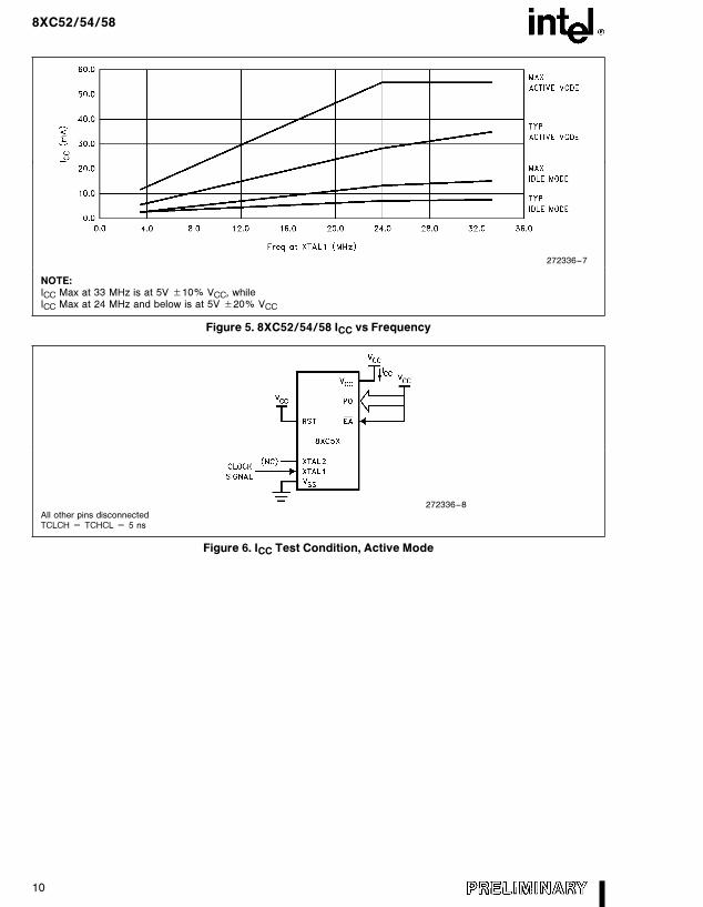
272336–7
NOTE:ICC Max at 33 MHz is at 5V g10% VCC, whileICC Max at 24 MHz and below is at 5V g20% VCC
Figure 5. 8XC52/54/58 ICC vs Frequency
272336–8All other pins disconnectedTCLCH e TCHCL e 5 ns
Figure 6. ICC Test Condition, Active Mode
10
8XC52/54/58
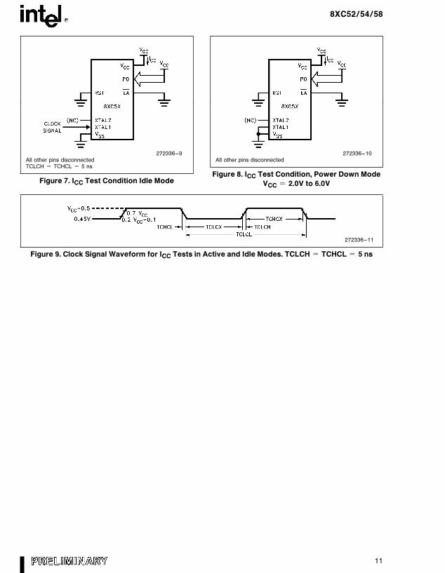
272336–9All other pins disconnectedTCLCH e TCHCL e 5 ns
Figure 7. ICC Test Condition Idle Mode
272336–10All other pins disconnected
Figure 8. ICC Test Condition, Power Down Mode
VCC e 2.0V to 6.0V
272336–11
Figure 9. Clock Signal Waveform for ICC Tests in Active and Idle Modes. TCLCH e TCHCL e 5 ns
11
8XC52/54/58
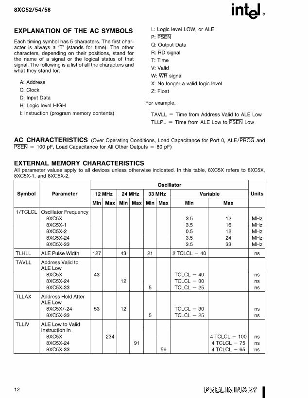
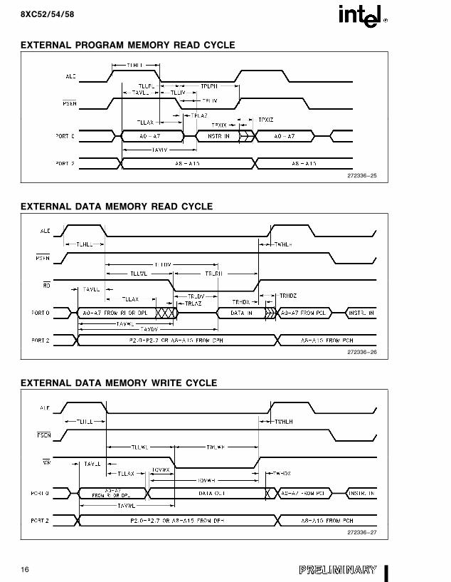
EXPLANATION OF THE AC SYMBOLS
Each timing symbol has 5 characters. The first char-acter is always a ‘T’ (stands for time). The othercharacters, depending on their positions, stand forthe name of a signal or the logical status of thatsignal. The following is a list of all the characters andwhat they stand for.
A: Address
C: Clock
D: Input Data
H: Logic level HIGH
I: Instruction (program memory contents)
L: Logic level LOW, or ALE
P: PSEN
Q: Output Data
R: RD signal
T: Time
V: Valid
W: WR signal
X: No longer a valid logic level
Z: Float
For example,
TAVLL e Time from Address Valid to ALE Low
TLLPL e Time from ALE Low to PSEN Low
AC CHARACTERISTICS (Over Operating Conditions, Load Capacitance for Port 0, ALE/PROG and
PSEN e 100 pF, Load Capacitance for All Other Outputs e 80 pF)
EXTERNAL MEMORY CHARACTERISTICSAll parameter values apply to all devices unless otherwise indicated. In this table, 8XC5X refers to 8XC5X,8XC5X-1, and 8XC5X-2.
Symbol Parameter
Oscillator
Units12 MHz 24 MHz 33 MHz Variable
Min Max Min Max Min Max Min Max
1/TCLCL Oscillator Frequency
8XC5X 3.5 12 MHz
8XC5X-1 3.5 16 MHz
8XC5X-2 0.5 12 MHz
8XC5X-24 3.5 24 MHz
8XC5X-33 3.5 33 MHz
TLHLL ALE Pulse Width 127 43 21 2 TCLCL b 40 ns
TAVLL Address Valid toALE Low
8XC5X 43 TCLCL b 40 ns
8XC5X-24 12 TCLCL b 30 ns
8XC5X-33 5 TCLCL b 25 ns
TLLAX Address Hold AfterALE Low
8XC5X/-24 53 12 TCLCL b 30 ns
8XC5X-33 5 TCLCL b 25 ns
TLLIV ALE Low to ValidInstruction In
8XC5X 234 4 TCLCL b 100 ns
8XC5X-24 91 4 TCLCL b 75 ns
8XC5X-33 56 4 TCLCL b 65 ns
12
8XC52/54/58
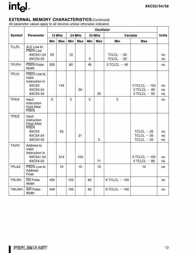
EXTERNAL MEMORY CHARACTERISTICS (Continued)
All parameter values apply to all devices unless otherwise indicated.
Symbol Parameter
Oscillator
Units12 MHz 24 MHz 33 MHz Variable
Min Max Min Max Min Max Min Max
TLLPL ALE Low toPSEN Low
8XC5X/-24 53 12 TCLCL b 30 ns
8XC5X-33 5 TCLCL b 25 ns
TPLPH PSEN Pulse 205 80 46 3 TCLCL b 45 nsWidth
TPLIV PSEN Low toValidInstruction In
8XC5X 145 3 TCLCL b 105 ns
8XC5X-24 35 3 TCLCL b 90 ns
8XC5X-33 35 3 TCLCL b 55 ns
TPXIX Input 0 0 0 0 nsInstructionHold AfterPSEN
TPXIZ InputInstructionFloat AfterPSEN
8XC5X 59 TCLCL b 25 ns
8XC5X-24 21 TCLCL b 20 ns
8XC5X-33 5 TCLCL b 25 ns
TAVIV Address toValidInstruction In
8XC5X/-24 312 103 5 TCLCL b 105 ns
8XC5X-33 71 5 TCLCL b 80 ns
TPLAZ PSEN Low to 10 10 10 10 nsAddressFloat
TRLRH RD Pulse 400 150 82 6 TCLCL b 100 nsWidth
TWLWH WR Pulse 400 150 82 6 TCLCL b 100 nsWidth
13
8XC52/54/58
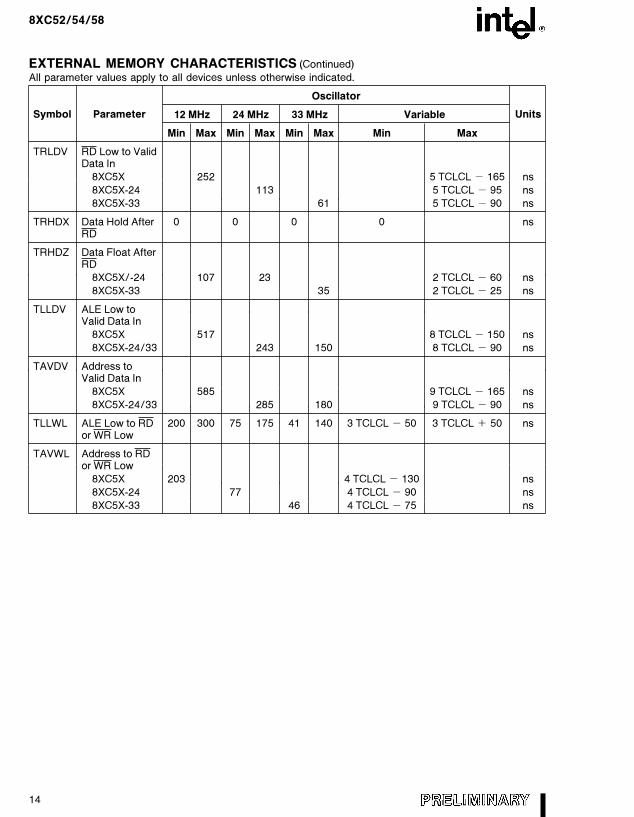
EXTERNAL MEMORY CHARACTERISTICS (Continued)
All parameter values apply to all devices unless otherwise indicated.
Symbol Parameter
Oscillator
Units12 MHz 24 MHz 33 MHz Variable
Min Max Min Max Min Max Min Max
TRLDV RD Low to ValidData In
8XC5X 252 5 TCLCL b 165 ns
8XC5X-24 113 5 TCLCL b 95 ns
8XC5X-33 61 5 TCLCL b 90 ns
TRHDX Data Hold After 0 0 0 0 nsRD
TRHDZ Data Float AfterRD
8XC5X/-24 107 23 2 TCLCL b 60 ns
8XC5X-33 35 2 TCLCL b 25 ns
TLLDV ALE Low toValid Data In
8XC5X 517 8 TCLCL b 150 ns
8XC5X-24/33 243 150 8 TCLCL b 90 ns
TAVDV Address toValid Data In
8XC5X 585 9 TCLCL b 165 ns
8XC5X-24/33 285 180 9 TCLCL b 90 ns
TLLWL ALE Low to RD 200 300 75 175 41 140 3 TCLCL b 50 3 TCLCL a 50 nsor WR Low
TAVWL Address to RDor WR Low
8XC5X 203 4 TCLCL b 130 ns
8XC5X-24 77 4 TCLCL b 90 ns
8XC5X-33 46 4 TCLCL b 75 ns
14
8XC52/54/58
EXTERNAL MEMORY CHARACTERISTICS (Continued)
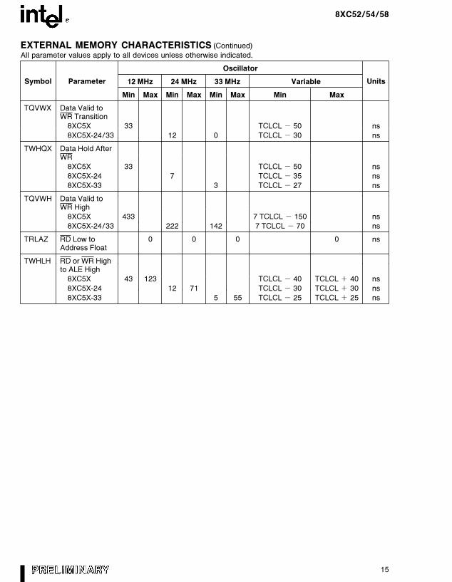
All parameter values apply to all devices unless otherwise indicated.
Symbol Parameter
Oscillator
Units12 MHz 24 MHz 33 MHz Variable
Min Max Min Max Min Max Min Max
TQVWX Data Valid toWR Transition
8XC5X 33 TCLCL b 50 ns
8XC5X-24/33 12 0 TCLCL b 30 ns
TWHQX Data Hold AfterWR
8XC5X 33 TCLCL b 50 ns
8XC5X-24 7 TCLCL b 35 ns
8XC5X-33 3 TCLCL b 27 ns
TQVWH Data Valid toWR High
8XC5X 433 7 TCLCL b 150 ns
8XC5X-24/33 222 142 7 TCLCL b 70 ns
TRLAZ RD Low to 0 0 0 0 nsAddress Float
TWHLH RD or WR Highto ALE High
8XC5X 43 123 TCLCL b 40 TCLCL a 40 ns
8XC5X-24 12 71 TCLCL b 30 TCLCL a 30 ns
8XC5X-33 5 55 TCLCL b 25 TCLCL a 25 ns
15
8XC52/54/58
EXTERNAL PROGRAM MEMORY READ CYCLE
272336–25
EXTERNAL DATA MEMORY READ CYCLE
272336–26
EXTERNAL DATA MEMORY WRITE CYCLE
272336–27
16
8XC52/54/58
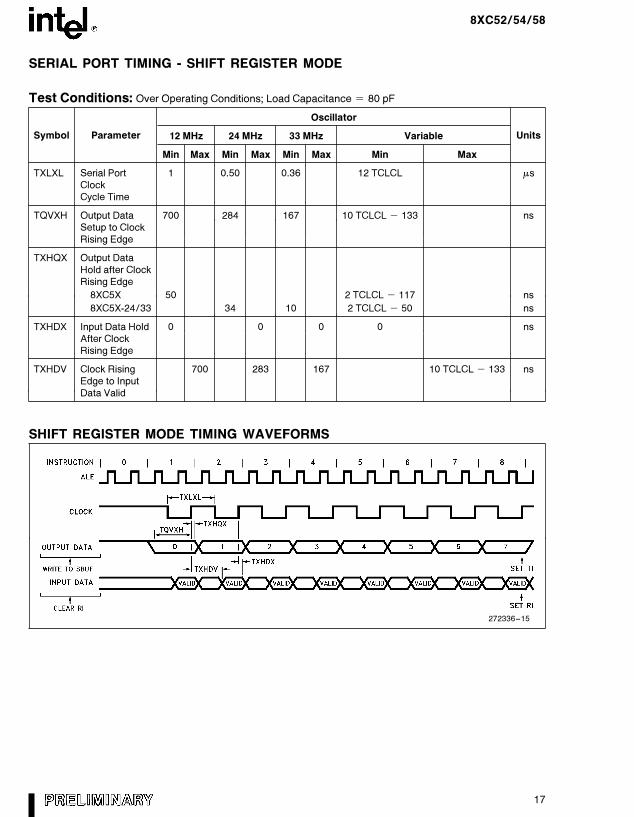
SERIAL PORT TIMING - SHIFT REGISTER MODE
Test Conditions: Over Operating Conditions; Load Capacitance e 80 pF
Symbol Parameter
Oscillator
Units12 MHz 24 MHz 33 MHz Variable
Min Max Min Max Min Max Min Max
TXLXL Serial Port 1 0.50 0.36 12 TCLCL msClockCycle Time
TQVXH Output Data 700 284 167 10 TCLCL b 133 nsSetup to ClockRising Edge
TXHQX Output DataHold after ClockRising Edge
8XC5X 50 2 TCLCL b 117 ns
8XC5X-24/33 34 10 2 TCLCL b 50 ns
TXHDX Input Data Hold 0 0 0 0 nsAfter ClockRising Edge
TXHDV Clock Rising 700 283 167 10 TCLCL b 133 nsEdge to InputData Valid
SHIFT REGISTER MODE TIMING WAVEFORMS
272336–15
17
8XC52/54/58
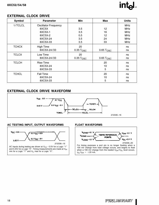
EXTERNAL CLOCK DRIVE
Symbol Parameter Min Max Units
1/TCLCL Oscillator Frequency MHz
8XC5X 3.5 12 MHz
8XC5X-1 3.5 16 MHz
8XC5X-2 0.5 12 MHz
8XC5X-24 3.5 24 MHz
8XC5X-33 3.5 33 MHz
TCHCX High Time 20 ns
8XC5X-24/33 0.35 TOSC 0.65 TOSC ns
TCLCX Low Time 20 ns
8XC5X-24/33 0.35 TOSC 0.65 TOSC ns
TCLCH Rise Time 20 ns
8XC5X-24 10 ns
8XC5X-33 5 ns
TCHCL Fall Time 20 ns
8XC5X-24 10 ns
8XC5X-33 5 ns
EXTERNAL CLOCK DRIVE WAVEFORM
272336–16
AC TESTING INPUT, OUTPUT WAVEFORMS
272336–19
AC Inputs during testing are driven at VCCb0.5V for a Logic ‘‘1’’and 0.45V for a Logic ‘‘0’’. Timing measurements are made at VIHmin for a Logic ‘‘1’’ and VIL max for a Logic ‘‘0’’.
FLOAT WAVEFORMS
272336–20For timing purposes a port pin is no longer floating when a100 mV change from load voltage occurs, and begins to floatwhen a 100 mV change from the loaded VOH/VOL level occurs.IOL/IOH e g20 mA.
18
8XC52/54/58
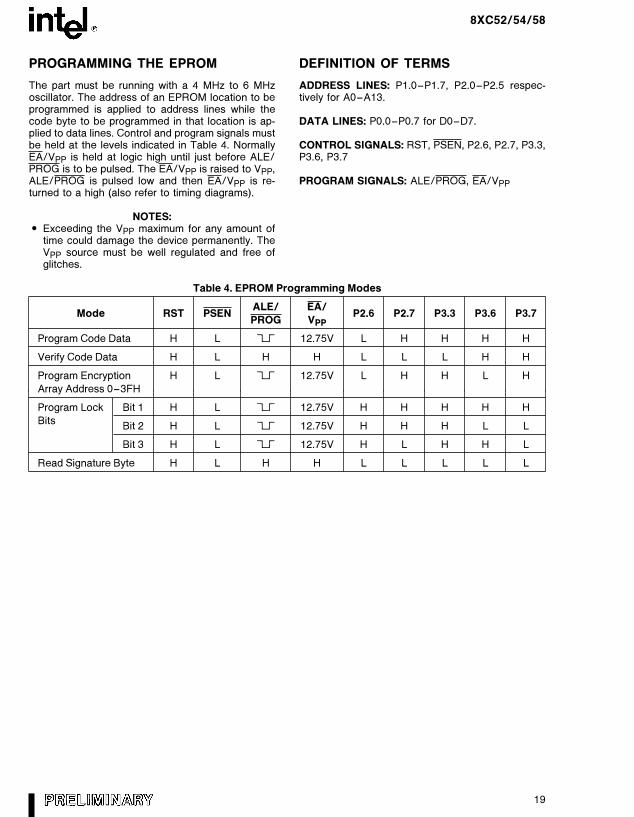
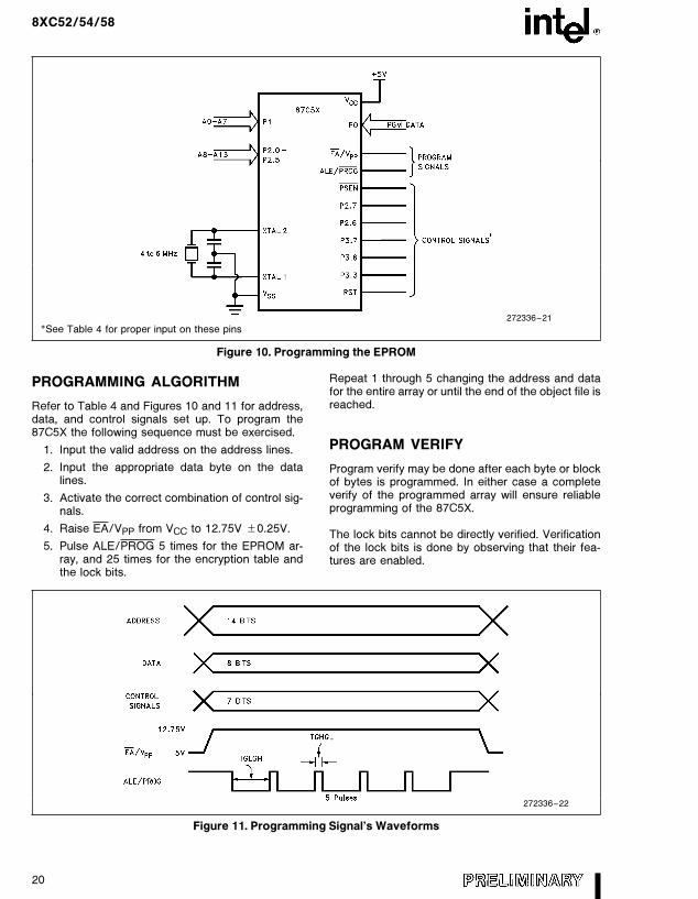
PROGRAMMING THE EPROM
The part must be running with a 4 MHz to 6 MHzoscillator. The address of an EPROM location to beprogrammed is applied to address lines while thecode byte to be programmed in that location is ap-plied to data lines. Control and program signals mustbe held at the levels indicated in Table 4. NormallyEA/VPP is held at logic high until just before ALE/PROG is to be pulsed. The EA/VPP is raised to VPP,ALE/PROG is pulsed low and then EA/VPP is re-turned to a high (also refer to timing diagrams).
NOTES:# Exceeding the VPP maximum for any amount of
time could damage the device permanently. TheVPP source must be well regulated and free ofglitches.
DEFINITION OF TERMS
ADDRESS LINES: P1.0–P1.7, P2.0–P2.5 respec-tively for A0–A13.
DATA LINES: P0.0–P0.7 for D0–D7.
CONTROL SIGNALS: RST, PSEN, P2.6, P2.7, P3.3,P3.6, P3.7
PROGRAM SIGNALS: ALE/PROG, EA/VPP
Table 4. EPROM Programming Modes
Mode RST PSENALE/ EA/
P2.6 P2.7 P3.3 P3.6 P3.7PROG VPP
Program Code Data H L ß 12.75V L H H H H
Verify Code Data H L H H L L L H H
Program Encryption H L ß 12.75V L H H L H
Array Address 0–3FH
Program Lock Bit 1 H L ß 12.75V H H H H H
BitsBit 2 H L ß 12.75V H H H L L
Bit 3 H L ß 12.75V H L H H L
Read Signature Byte H L H H L L L L L
19
8XC52/54/58
272336–21
*See Table 4 for proper input on these pins
Figure 10. Programming the EPROM
PROGRAMMING ALGORITHM
Refer to Table 4 and Figures 10 and 11 for address,data, and control signals set up. To program the87C5X the following sequence must be exercised.
1. Input the valid address on the address lines.
2. Input the appropriate data byte on the datalines.
3. Activate the correct combination of control sig-nals.
4. Raise EA/VPP from VCC to 12.75V g0.25V.
5. Pulse ALE/PROG 5 times for the EPROM ar-ray, and 25 times for the encryption table andthe lock bits.
Repeat 1 through 5 changing the address and datafor the entire array or until the end of the object file isreached.
PROGRAM VERIFY
Program verify may be done after each byte or blockof bytes is programmed. In either case a completeverify of the programmed array will ensure reliableprogramming of the 87C5X.
The lock bits cannot be directly verified. Verificationof the lock bits is done by observing that their fea-tures are enabled.
272336–22
Figure 11. Programming Signal’s Waveforms
20
8XC52/54/58
ROM and EPROM Lock System
The program lock system, when programmed, pro-tects the onboard program against software piracy.
The 80C5X has a one-level program lock systemand a 64-byte encryption table. See line 2 of Table5. If program protection is desired. the user submitsthe encryption table with their code. and both thelock-bit and encryption array are programmed by thefactory. The encryption array is not available withoutthe lock bit. For the lock bit to be programmed, theuser must submit an encryption table.
The 87C5X has a 3-level program lock system and a64-byte encryption array. Since this is an EPROMdevice, all locations are user-programmable. SeeTable 5.
Encryption Array
Within the EPROM array are 64 bytes of EncryptionArray that are initially unprogrammed (all 1’s). Everytime that a byte is addressed during a verify, 6 ad-dress lines are used to select a byte of the Encryp-tion Array. This byte is then exclusive-NOR’ed(XNOR) with the code byte, creating an EncryptionVerify byte. The algorithm, with the array in the un-programmed state (all 1’s), will return the code in itsoriginal, unmodified form. For programming the En-cryption Array, refer to Table 4 (Programming theEPROM).
When using the encryption array, one important fac-tor needs to be considered. If a code byte has thevalue 0FFH, verifying the byte will produce the en-cryption byte value. If a large block (l64 bytes) ofcode is left unprogrammed, a verification routine willdisplay the contents of the encryption array. For thisreason all unused code bytes should be pro-grammed with some value other than 0FFH, and notall of them the same value. This will ensure maxi-mum program protection.
Program Lock Bits
The 87C5X has 3 programmable lock bits that whenprogrammed according to Table 5 will provide differ-ent levels of protection for the on-chip code anddata.
Erasing the EPROM also erases the encryption ar-ray and the program lock bits, returning the part tofull functionality.
Reading the Signature Bytes
The 8XC5X has 3 signature bytes in locations 30H,31H, and 60H. To read these bytes follow the proce-dure for EPROM verify, but activate the control linesprovided in Table 4 for Read Signature Byte.
Location Device Contents
30H All 89H
31H All 58H
60H 80C52 12H
87C52 52H
80C54 14H
87C54 54H
80C58 18H
87C58 58H
Erasure Characteristics(Windowed Packages Only)
Erasure of the EPROM begins to occur when thechip is exposed to light with wavelength shorter thanapproximately 4,000 Angstroms. Since sunlight andfluorescent lighting have wavelengths in this range,exposure to these light sources over an extendedtime (about 1 week in sunlight, or 3 years in room-level fluorescent lighting) could cause inadvertenterasure. If an application subjects the device to thistype of exposure, it is suggested that an opaque la-bel be placed over the window.
The recommended erasure procedure is exposureto ultraviolet light (at 2537 Angstroms) to an integrat-ed dose of at least 15 W-sec/cm2. Exposing theEPROM to an ultraviolet lamp of 12,000 mW/cm2
rating for 30 minutes, at a distance of about 1 inch,should be sufficient.
Erasure leaves all the EPROM Cells in a 1’s state.
21
8XC52/54/58
Table 5. Program Lock Bits and the Features
Program Lock BitsProtection Type
LB1 LB2 LB3
1 U U U No Program Lock features enabled. (Code verify will still be encrypted by theEncryption Array if programmed.)
2 P U U MOVC instructions executed from external program memory are disabled fromfetching code bytes from internal memory, EA is sampled and latched onReset, and further programming of the EPROM is disabled.
3 P P U Same as 2, also verify is disabled.
4 P P P Same as 3, also external execution is disabled.
NOTE:Any other combination of the lock bits is not defined.
EPROM PROGRAMMING AND VERIFICATION CHARACTERISTICS(TA e 21§C to 27§C; VCC e 5V g20%; VSS e 0V)
Symbol Parameter Min Max Units
VPP Programming Supply Voltage 12.5 13.0 V
IPP Programming Supply Current 75 mA
1/TCLCL Oscillator Frequency 4 6 MHz
TAVGL Address Setup to PROG Low 48TCLCL
TGHAX Address Hold after PROG 48TCLCL
TDVGL Data Setup to PROG Low 48TCLCL
TGHDX Data Hold after PROG 48TCLCL
TEHSH (Enable) High to VPP 48TCLCL
TSHGL VPP Setup to PROG Low 10 ms
TGHSL VPP Hold after PROG 10 ms
TGLGH PROG Width 90 110 ms
TAVQV Address to Data Valid 48TCLCL
TELQV ENABLE Low to Data Valid 48TCLCL
TEHQZ Data Float after ENABLE 0 48TCLCL
TGHGL PROG High to PROG Low 10 ms
22
8XC52/54/58
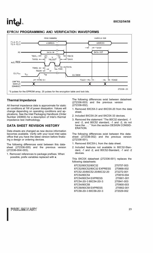
EPROM PROGRAMMING AND VERIFICATION WAVEFORMS
272336–23*5 pulses for the EPROM array. 25 pulses for the encryption table and lock bits.
Thermal ImpedanceAll thermal impedance data is approximate for staticair conditions at 1W of power dissipation. Values willchange depending on operating conditions and ap-plications. See the Intel Packaging Handbook (OrderNumber 240800) for a description of Intel’s thermalimpedance test methodology.
DATA SHEET REVISION HISTORYData sheets are changed as new device informationbecomes available. Verify with your local Intel salesoffice that you have the latest version before finaliz-ing a design or ordering devices.
The following differences exist between datasheet(272336-003) and the previous version(272336-002).1. Removed 8XC5X-3 and 8XC5X-20 from the data
sheet.2. Included 8XC5X-24 and 8XC5X-33 devices.3. Removed the statement ‘‘The 80C32 standard, -1
and -2, and 80C52 standard, -1 and -2, do nothave the . . . ’’ from the section DESIGN CONSID-ERATION.
The following differences exist between this data-sheet (272336-002) and the previous version(272336-001).1. Removed 8XC5X-L from the data sheet.2. Included features not available in 80C32-Stan-
dard, -1 and -2, and 80C52-Standard, -1 and -2devices.
This 8XC5X datasheet (272336-001) replaces thefollowing datasheets:
87C52/80C52/80C32 270757-00387C52/80C52/80C32 EXPRESS 270868-00287C52-20/80C52-20/80C32-20 272272-00187C54/80C54 270816-00487C54/80C54 EXPRESS 270901-00187C54-20/-3 80C54-20/-3 270941-00387C54/80C58 270900-00387C58/80C58 EXPRESS 270902-00187C58-20/-3 80C58-20/-3 272029-002
23
The following differences exist between this data-sheet (272336-005) and the previous version(272336-004/-003).1. Removed references to package prefixes. When possible, prefix variables replaced with x.