Embed Size (px)
Citation preview
*Other brands and names are the property of their respective owners.Information in this document is provided in connection with Intel products. Intel assumes no liability whatsoever, including infringement of any patent orcopyright, for sale and use of Intel products except as provided in Intel’s Terms and Conditions of Sale for such products. Intel retains the right to makechanges to these specifications at any time, without notice. Microcomputer Products may have minor variations to this specification known as errata.
December 1995COPYRIGHT © INTEL CORPORATION, 1995 Order Number: 231630-011
Intel386TM DX MICROPROCESSOR32-BIT CHMOS MICROPROCESSOR
WITH INTEGRATED MEMORY MANAGEMENTY Flexible 32-Bit Microprocessor
Ð 8, 16, 32-Bit Data TypesÐ 8 General Purpose 32-Bit Registers
Y Very Large Address SpaceÐ 4 Gigabyte PhysicalÐ 64 Terabyte VirtualÐ 4 Gigabyte Maximum Segment Size
Y Integrated Memory Management UnitÐ Virtual Memory SupportÐ Optional On-Chip PagingÐ 4 Levels of ProtectionÐ Fully Compatible with 80286
Y Object Code Compatible with All 8086Family Microprocessors
Y Virtual 8086 Mode Allows Running of8086 Software in a Protected andPaged System
Y Hardware Debugging Support
Y Optimized for System PerformanceÐ Pipelined Instruction ExecutionÐ On-Chip Address Translation CachesÐ 20, 25 and 33 MHz ClockÐ 40, 50 and 66 Megabytes/Sec Bus
Bandwidth
Y Numerics Support via Intel387TM DXMath Coprocessor
Y Complete System DevelopmentSupportÐ Software: C, PL/M, Assembler
System Generation ToolsÐ Debuggers: PSCOPE, ICETM-386
Y High Speed CHMOS IV Technology
Y 132 Pin Grid Array Package
Y 132 Pin Plastic Quad Flat Package(See Packaging Specification, Order Ý231369)
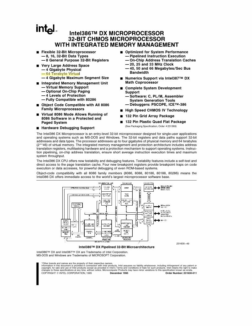
The Intel386 DX Microprocessor is an entry-level 32-bit microprocessor designed for single-user applicationsand operating systems such as MS-DOS and Windows. The 32-bit registers and data paths support 32-bitaddresses and data types. The processor addresses up to four gigabytes of physical memory and 64 terabytes(2**46) of virtual memory. The integrated memory management and protection architecture includes addresstranslation registers, multitasking hardware and a protection mechanism to support operating systems. Instruc-tion pipelining, on-chip address translation, ensure short average instruction execution times and maximumsystem throughput.
The Intel386 DX CPU offers new testability and debugging features. Testability features include a self-test anddirect access to the page translation cache. Four new breakpoint registers provide breakpoint traps on codeexecution or data accesses, for powerful debugging of even ROM-based systems.
Object-code compatibility with all 8086 family members (8086, 8088, 80186, 80188, 80286) means theIntel386 DX offers immediate access to the world’s largest microprocessor software base.
231630–49
Intel386TM DX Pipelined 32-Bit Microarchitecture
Intel386TM DX and Intel387TM DX are Trademarks of Intel Corporation.MS-DOS and Windows are Trademarks of MICROSOFT Corporation.


Intel386TM DX MICROPROCESSOR32-BIT CHMOS MICROPROCESSOR
WITH INTEGRATED MEMORY MANAGEMENT
CONTENTS PAGE
1. PIN ASSIGNMENT ÀÀÀÀÀÀÀÀÀÀÀÀÀÀÀÀÀÀÀÀÀÀÀÀÀÀÀÀÀÀÀÀÀÀÀÀÀÀÀÀÀÀÀÀÀÀÀÀÀÀÀÀÀÀÀÀÀÀÀÀÀÀÀÀÀÀÀÀÀÀÀÀÀ 5
1.1 Pin Description Table ÀÀÀÀÀÀÀÀÀÀÀÀÀÀÀÀÀÀÀÀÀÀÀÀÀÀÀÀÀÀÀÀÀÀÀÀÀÀÀÀÀÀÀÀÀÀÀÀÀÀÀÀÀÀÀÀÀÀÀÀÀÀÀÀÀÀ 6
2. BASE ARCHITECTURE ÀÀÀÀÀÀÀÀÀÀÀÀÀÀÀÀÀÀÀÀÀÀÀÀÀÀÀÀÀÀÀÀÀÀÀÀÀÀÀÀÀÀÀÀÀÀÀÀÀÀÀÀÀÀÀÀÀÀÀÀÀÀÀÀÀÀÀ 8
2.1 Introduction ÀÀÀÀÀÀÀÀÀÀÀÀÀÀÀÀÀÀÀÀÀÀÀÀÀÀÀÀÀÀÀÀÀÀÀÀÀÀÀÀÀÀÀÀÀÀÀÀÀÀÀÀÀÀÀÀÀÀÀÀÀÀÀÀÀÀÀÀÀÀÀÀÀÀÀÀ 8
2.2 Register Overview ÀÀÀÀÀÀÀÀÀÀÀÀÀÀÀÀÀÀÀÀÀÀÀÀÀÀÀÀÀÀÀÀÀÀÀÀÀÀÀÀÀÀÀÀÀÀÀÀÀÀÀÀÀÀÀÀÀÀÀÀÀÀÀÀÀÀÀÀÀ 8
2.3 Register Descriptions ÀÀÀÀÀÀÀÀÀÀÀÀÀÀÀÀÀÀÀÀÀÀÀÀÀÀÀÀÀÀÀÀÀÀÀÀÀÀÀÀÀÀÀÀÀÀÀÀÀÀÀÀÀÀÀÀÀÀÀÀÀÀÀÀÀÀ 9
2.4 Instruction Set ÀÀÀÀÀÀÀÀÀÀÀÀÀÀÀÀÀÀÀÀÀÀÀÀÀÀÀÀÀÀÀÀÀÀÀÀÀÀÀÀÀÀÀÀÀÀÀÀÀÀÀÀÀÀÀÀÀÀÀÀÀÀÀÀÀÀÀÀÀÀÀÀ 15
2.5 Addressing Modes ÀÀÀÀÀÀÀÀÀÀÀÀÀÀÀÀÀÀÀÀÀÀÀÀÀÀÀÀÀÀÀÀÀÀÀÀÀÀÀÀÀÀÀÀÀÀÀÀÀÀÀÀÀÀÀÀÀÀÀÀÀÀÀÀÀÀÀÀ 18
2.6 Data Types ÀÀÀÀÀÀÀÀÀÀÀÀÀÀÀÀÀÀÀÀÀÀÀÀÀÀÀÀÀÀÀÀÀÀÀÀÀÀÀÀÀÀÀÀÀÀÀÀÀÀÀÀÀÀÀÀÀÀÀÀÀÀÀÀÀÀÀÀÀÀÀÀÀÀÀ 20
2.7 Memory Organization ÀÀÀÀÀÀÀÀÀÀÀÀÀÀÀÀÀÀÀÀÀÀÀÀÀÀÀÀÀÀÀÀÀÀÀÀÀÀÀÀÀÀÀÀÀÀÀÀÀÀÀÀÀÀÀÀÀÀÀÀÀÀÀÀÀ 22
2.8 I/O Space ÀÀÀÀÀÀÀÀÀÀÀÀÀÀÀÀÀÀÀÀÀÀÀÀÀÀÀÀÀÀÀÀÀÀÀÀÀÀÀÀÀÀÀÀÀÀÀÀÀÀÀÀÀÀÀÀÀÀÀÀÀÀÀÀÀÀÀÀÀÀÀÀÀÀÀÀ 23
2.9 Interrupts ÀÀÀÀÀÀÀÀÀÀÀÀÀÀÀÀÀÀÀÀÀÀÀÀÀÀÀÀÀÀÀÀÀÀÀÀÀÀÀÀÀÀÀÀÀÀÀÀÀÀÀÀÀÀÀÀÀÀÀÀÀÀÀÀÀÀÀÀÀÀÀÀÀÀÀÀÀ 24
2.10 Reset and Initialization ÀÀÀÀÀÀÀÀÀÀÀÀÀÀÀÀÀÀÀÀÀÀÀÀÀÀÀÀÀÀÀÀÀÀÀÀÀÀÀÀÀÀÀÀÀÀÀÀÀÀÀÀÀÀÀÀÀÀÀÀÀÀÀ 27
2.11 Testability ÀÀÀÀÀÀÀÀÀÀÀÀÀÀÀÀÀÀÀÀÀÀÀÀÀÀÀÀÀÀÀÀÀÀÀÀÀÀÀÀÀÀÀÀÀÀÀÀÀÀÀÀÀÀÀÀÀÀÀÀÀÀÀÀÀÀÀÀÀÀÀÀÀÀÀ 28
2.12 Debugging Support ÀÀÀÀÀÀÀÀÀÀÀÀÀÀÀÀÀÀÀÀÀÀÀÀÀÀÀÀÀÀÀÀÀÀÀÀÀÀÀÀÀÀÀÀÀÀÀÀÀÀÀÀÀÀÀÀÀÀÀÀÀÀÀÀÀÀ 28
3. REAL MODE ARCHITECTURE ÀÀÀÀÀÀÀÀÀÀÀÀÀÀÀÀÀÀÀÀÀÀÀÀÀÀÀÀÀÀÀÀÀÀÀÀÀÀÀÀÀÀÀÀÀÀÀÀÀÀÀÀÀÀÀÀÀÀÀ 32
3.1 Real Mode Introduction ÀÀÀÀÀÀÀÀÀÀÀÀÀÀÀÀÀÀÀÀÀÀÀÀÀÀÀÀÀÀÀÀÀÀÀÀÀÀÀÀÀÀÀÀÀÀÀÀÀÀÀÀÀÀÀÀÀÀÀÀÀÀÀ 32
3.2 Memory Addressing ÀÀÀÀÀÀÀÀÀÀÀÀÀÀÀÀÀÀÀÀÀÀÀÀÀÀÀÀÀÀÀÀÀÀÀÀÀÀÀÀÀÀÀÀÀÀÀÀÀÀÀÀÀÀÀÀÀÀÀÀÀÀÀÀÀÀÀ 33
3.3 Reserved Locations ÀÀÀÀÀÀÀÀÀÀÀÀÀÀÀÀÀÀÀÀÀÀÀÀÀÀÀÀÀÀÀÀÀÀÀÀÀÀÀÀÀÀÀÀÀÀÀÀÀÀÀÀÀÀÀÀÀÀÀÀÀÀÀÀÀÀÀ 34
3.4 Interrupts ÀÀÀÀÀÀÀÀÀÀÀÀÀÀÀÀÀÀÀÀÀÀÀÀÀÀÀÀÀÀÀÀÀÀÀÀÀÀÀÀÀÀÀÀÀÀÀÀÀÀÀÀÀÀÀÀÀÀÀÀÀÀÀÀÀÀÀÀÀÀÀÀÀÀÀÀÀ 34
3.5 Shutdown and Halt ÀÀÀÀÀÀÀÀÀÀÀÀÀÀÀÀÀÀÀÀÀÀÀÀÀÀÀÀÀÀÀÀÀÀÀÀÀÀÀÀÀÀÀÀÀÀÀÀÀÀÀÀÀÀÀÀÀÀÀÀÀÀÀÀÀÀÀÀ 34
4. PROTECTED MODE ARCHITECTURE ÀÀÀÀÀÀÀÀÀÀÀÀÀÀÀÀÀÀÀÀÀÀÀÀÀÀÀÀÀÀÀÀÀÀÀÀÀÀÀÀÀÀÀÀÀÀÀÀÀÀÀ 34
4.1 Introduction ÀÀÀÀÀÀÀÀÀÀÀÀÀÀÀÀÀÀÀÀÀÀÀÀÀÀÀÀÀÀÀÀÀÀÀÀÀÀÀÀÀÀÀÀÀÀÀÀÀÀÀÀÀÀÀÀÀÀÀÀÀÀÀÀÀÀÀÀÀÀÀÀÀÀÀ 34
4.2 Addressing Mechanism ÀÀÀÀÀÀÀÀÀÀÀÀÀÀÀÀÀÀÀÀÀÀÀÀÀÀÀÀÀÀÀÀÀÀÀÀÀÀÀÀÀÀÀÀÀÀÀÀÀÀÀÀÀÀÀÀÀÀÀÀÀÀÀ 35
4.3 Segmentation ÀÀÀÀÀÀÀÀÀÀÀÀÀÀÀÀÀÀÀÀÀÀÀÀÀÀÀÀÀÀÀÀÀÀÀÀÀÀÀÀÀÀÀÀÀÀÀÀÀÀÀÀÀÀÀÀÀÀÀÀÀÀÀÀÀÀÀÀÀÀÀÀÀ 36
4.4 Protection ÀÀÀÀÀÀÀÀÀÀÀÀÀÀÀÀÀÀÀÀÀÀÀÀÀÀÀÀÀÀÀÀÀÀÀÀÀÀÀÀÀÀÀÀÀÀÀÀÀÀÀÀÀÀÀÀÀÀÀÀÀÀÀÀÀÀÀÀÀÀÀÀÀÀÀÀ 46
4.5 Paging ÀÀÀÀÀÀÀÀÀÀÀÀÀÀÀÀÀÀÀÀÀÀÀÀÀÀÀÀÀÀÀÀÀÀÀÀÀÀÀÀÀÀÀÀÀÀÀÀÀÀÀÀÀÀÀÀÀÀÀÀÀÀÀÀÀÀÀÀÀÀÀÀÀÀÀÀÀÀÀÀ 52
4.6 Virtual 8086 Environment ÀÀÀÀÀÀÀÀÀÀÀÀÀÀÀÀÀÀÀÀÀÀÀÀÀÀÀÀÀÀÀÀÀÀÀÀÀÀÀÀÀÀÀÀÀÀÀÀÀÀÀÀÀÀÀÀÀÀÀÀÀ 56
5. FUNCTIONAL DATA ÀÀÀÀÀÀÀÀÀÀÀÀÀÀÀÀÀÀÀÀÀÀÀÀÀÀÀÀÀÀÀÀÀÀÀÀÀÀÀÀÀÀÀÀÀÀÀÀÀÀÀÀÀÀÀÀÀÀÀÀÀÀÀÀÀÀÀÀÀ 61
5.1 Introduction ÀÀÀÀÀÀÀÀÀÀÀÀÀÀÀÀÀÀÀÀÀÀÀÀÀÀÀÀÀÀÀÀÀÀÀÀÀÀÀÀÀÀÀÀÀÀÀÀÀÀÀÀÀÀÀÀÀÀÀÀÀÀÀÀÀÀÀÀÀÀÀÀÀÀÀ 61
5.2 Signal Description ÀÀÀÀÀÀÀÀÀÀÀÀÀÀÀÀÀÀÀÀÀÀÀÀÀÀÀÀÀÀÀÀÀÀÀÀÀÀÀÀÀÀÀÀÀÀÀÀÀÀÀÀÀÀÀÀÀÀÀÀÀÀÀÀÀÀÀÀ 61
5.2.1 Introduction ÀÀÀÀÀÀÀÀÀÀÀÀÀÀÀÀÀÀÀÀÀÀÀÀÀÀÀÀÀÀÀÀÀÀÀÀÀÀÀÀÀÀÀÀÀÀÀÀÀÀÀÀÀÀÀÀÀÀÀÀÀÀÀÀÀÀÀÀÀ 61
5.2.2 Clock (CLK2) ÀÀÀÀÀÀÀÀÀÀÀÀÀÀÀÀÀÀÀÀÀÀÀÀÀÀÀÀÀÀÀÀÀÀÀÀÀÀÀÀÀÀÀÀÀÀÀÀÀÀÀÀÀÀÀÀÀÀÀÀÀÀÀÀÀÀÀÀ 62
5.2.3 Data Bus (D0 through D31) ÀÀÀÀÀÀÀÀÀÀÀÀÀÀÀÀÀÀÀÀÀÀÀÀÀÀÀÀÀÀÀÀÀÀÀÀÀÀÀÀÀÀÀÀÀÀÀÀÀÀÀÀÀÀ 62
5.2.4 Address Bus (BEOÝ through BE3Ý, A2 through A31) ÀÀÀÀÀÀÀÀÀÀÀÀÀÀÀÀÀÀÀÀÀÀÀÀÀÀÀÀ 62
5.2.5 Bus Cycle Definition Signals (W/RÝ, D/CÝ, M/IO, LOCKÝ) ÀÀÀÀÀÀÀÀÀÀÀÀÀÀÀÀÀÀÀÀÀ 63
5.2.6 Bus Control Signals (ADSÝ, READYÝ, NAÝ, BS16Ý) ÀÀÀÀÀÀÀÀÀÀÀÀÀÀÀÀÀÀÀÀÀÀÀÀÀÀÀ 64
5.2.7 Bus Arbitration Signals (HOLD, HLDA) ÀÀÀÀÀÀÀÀÀÀÀÀÀÀÀÀÀÀÀÀÀÀÀÀÀÀÀÀÀÀÀÀÀÀÀÀÀÀÀÀÀÀÀ 65
5.2.8 Coprocessor Interface Signals (PEREQ, BUSYÝ, ERRORÝ) ÀÀÀÀÀÀÀÀÀÀÀÀÀÀÀÀÀÀÀÀÀ 65
5.2.9 Interrupt Signals (INTR, NMI, RESET) ÀÀÀÀÀÀÀÀÀÀÀÀÀÀÀÀÀÀÀÀÀÀÀÀÀÀÀÀÀÀÀÀÀÀÀÀÀÀÀÀÀÀÀÀ 66
5.2.10 Signal Summary ÀÀÀÀÀÀÀÀÀÀÀÀÀÀÀÀÀÀÀÀÀÀÀÀÀÀÀÀÀÀÀÀÀÀÀÀÀÀÀÀÀÀÀÀÀÀÀÀÀÀÀÀÀÀÀÀÀÀÀÀÀÀÀÀ 67
3
CONTENTS PAGE
5. FUNCTIONAL DATA (Continued)5.3. Bus Transfer Mechanism ÀÀÀÀÀÀÀÀÀÀÀÀÀÀÀÀÀÀÀÀÀÀÀÀÀÀÀÀÀÀÀÀÀÀÀÀÀÀÀÀÀÀÀÀÀÀÀÀÀÀÀÀÀÀÀÀÀÀÀÀÀ 67
5.3.1 Introduction ÀÀÀÀÀÀÀÀÀÀÀÀÀÀÀÀÀÀÀÀÀÀÀÀÀÀÀÀÀÀÀÀÀÀÀÀÀÀÀÀÀÀÀÀÀÀÀÀÀÀÀÀÀÀÀÀÀÀÀÀÀÀÀÀÀÀÀÀÀ 67
5.3.2 Memory and I/O Spaces ÀÀÀÀÀÀÀÀÀÀÀÀÀÀÀÀÀÀÀÀÀÀÀÀÀÀÀÀÀÀÀÀÀÀÀÀÀÀÀÀÀÀÀÀÀÀÀÀÀÀÀÀÀÀÀÀÀ 68
5.3.3 Memory and I/O Organization ÀÀÀÀÀÀÀÀÀÀÀÀÀÀÀÀÀÀÀÀÀÀÀÀÀÀÀÀÀÀÀÀÀÀÀÀÀÀÀÀÀÀÀÀÀÀÀÀÀÀÀ 69
5.3.4 Dynamic Data Bus Sizing ÀÀÀÀÀÀÀÀÀÀÀÀÀÀÀÀÀÀÀÀÀÀÀÀÀÀÀÀÀÀÀÀÀÀÀÀÀÀÀÀÀÀÀÀÀÀÀÀÀÀÀÀÀÀÀÀ 69
5.3.5 Interfacing with 32- and 16-bit Memories ÀÀÀÀÀÀÀÀÀÀÀÀÀÀÀÀÀÀÀÀÀÀÀÀÀÀÀÀÀÀÀÀÀÀÀÀÀÀÀÀÀ 70
5.3.6 Operand Alignment ÀÀÀÀÀÀÀÀÀÀÀÀÀÀÀÀÀÀÀÀÀÀÀÀÀÀÀÀÀÀÀÀÀÀÀÀÀÀÀÀÀÀÀÀÀÀÀÀÀÀÀÀÀÀÀÀÀÀÀÀÀÀ 71
5.4 Bus Functional Description ÀÀÀÀÀÀÀÀÀÀÀÀÀÀÀÀÀÀÀÀÀÀÀÀÀÀÀÀÀÀÀÀÀÀÀÀÀÀÀÀÀÀÀÀÀÀÀÀÀÀÀÀÀÀÀÀÀÀÀÀ 71
5.4.1 Introduction ÀÀÀÀÀÀÀÀÀÀÀÀÀÀÀÀÀÀÀÀÀÀÀÀÀÀÀÀÀÀÀÀÀÀÀÀÀÀÀÀÀÀÀÀÀÀÀÀÀÀÀÀÀÀÀÀÀÀÀÀÀÀÀÀÀÀÀÀÀ 71
5.4.2 Address Pipelining ÀÀÀÀÀÀÀÀÀÀÀÀÀÀÀÀÀÀÀÀÀÀÀÀÀÀÀÀÀÀÀÀÀÀÀÀÀÀÀÀÀÀÀÀÀÀÀÀÀÀÀÀÀÀÀÀÀÀÀÀÀÀÀ 74
5.4.3 Read and Write Cycles ÀÀÀÀÀÀÀÀÀÀÀÀÀÀÀÀÀÀÀÀÀÀÀÀÀÀÀÀÀÀÀÀÀÀÀÀÀÀÀÀÀÀÀÀÀÀÀÀÀÀÀÀÀÀÀÀÀÀ 76
5.4.4 Interrupt Acknowledge (INTA) Cycles ÀÀÀÀÀÀÀÀÀÀÀÀÀÀÀÀÀÀÀÀÀÀÀÀÀÀÀÀÀÀÀÀÀÀÀÀÀÀÀÀÀÀÀÀ 87
5.4.5 Halt Indication Cycle ÀÀÀÀÀÀÀÀÀÀÀÀÀÀÀÀÀÀÀÀÀÀÀÀÀÀÀÀÀÀÀÀÀÀÀÀÀÀÀÀÀÀÀÀÀÀÀÀÀÀÀÀÀÀÀÀÀÀÀÀÀ 88
5.4.6 Shutdown Indication Cycle ÀÀÀÀÀÀÀÀÀÀÀÀÀÀÀÀÀÀÀÀÀÀÀÀÀÀÀÀÀÀÀÀÀÀÀÀÀÀÀÀÀÀÀÀÀÀÀÀÀÀÀÀÀÀÀ 89
5.5 Other Functional Descriptions ÀÀÀÀÀÀÀÀÀÀÀÀÀÀÀÀÀÀÀÀÀÀÀÀÀÀÀÀÀÀÀÀÀÀÀÀÀÀÀÀÀÀÀÀÀÀÀÀÀÀÀÀÀÀÀÀÀ 90
5.5.1 Entering and Exiting Hold Acknowledge ÀÀÀÀÀÀÀÀÀÀÀÀÀÀÀÀÀÀÀÀÀÀÀÀÀÀÀÀÀÀÀÀÀÀÀÀÀÀÀÀÀÀ 90
5.5.2 Reset during Hold Acknowledge ÀÀÀÀÀÀÀÀÀÀÀÀÀÀÀÀÀÀÀÀÀÀÀÀÀÀÀÀÀÀÀÀÀÀÀÀÀÀÀÀÀÀÀÀÀÀÀÀÀ 90
5.5.3 Bus Activity During and Following Reset ÀÀÀÀÀÀÀÀÀÀÀÀÀÀÀÀÀÀÀÀÀÀÀÀÀÀÀÀÀÀÀÀÀÀÀÀÀÀÀÀÀ 90
5.6 Self-test Signature ÀÀÀÀÀÀÀÀÀÀÀÀÀÀÀÀÀÀÀÀÀÀÀÀÀÀÀÀÀÀÀÀÀÀÀÀÀÀÀÀÀÀÀÀÀÀÀÀÀÀÀÀÀÀÀÀÀÀÀÀÀÀÀÀÀÀÀÀ 92
5.7 Component and Revision Identifiers ÀÀÀÀÀÀÀÀÀÀÀÀÀÀÀÀÀÀÀÀÀÀÀÀÀÀÀÀÀÀÀÀÀÀÀÀÀÀÀÀÀÀÀÀÀÀÀÀÀÀÀ 92
5.8 Coprocessor Interface ÀÀÀÀÀÀÀÀÀÀÀÀÀÀÀÀÀÀÀÀÀÀÀÀÀÀÀÀÀÀÀÀÀÀÀÀÀÀÀÀÀÀÀÀÀÀÀÀÀÀÀÀÀÀÀÀÀÀÀÀÀÀÀÀ 94
5.8.1 Software Testing for Coprocessor Presence ÀÀÀÀÀÀÀÀÀÀÀÀÀÀÀÀÀÀÀÀÀÀÀÀÀÀÀÀÀÀÀÀÀÀÀÀÀ 94
6. INSTRUCTION SET ÀÀÀÀÀÀÀÀÀÀÀÀÀÀÀÀÀÀÀÀÀÀÀÀÀÀÀÀÀÀÀÀÀÀÀÀÀÀÀÀÀÀÀÀÀÀÀÀÀÀÀÀÀÀÀÀÀÀÀÀÀÀÀÀÀÀÀÀÀÀ 95
6.1 Instruction Encoding and Clock Count Summary ÀÀÀÀÀÀÀÀÀÀÀÀÀÀÀÀÀÀÀÀÀÀÀÀÀÀÀÀÀÀÀÀÀÀÀÀÀÀÀ 95
6.2 Instruction Encoding Details ÀÀÀÀÀÀÀÀÀÀÀÀÀÀÀÀÀÀÀÀÀÀÀÀÀÀÀÀÀÀÀÀÀÀÀÀÀÀÀÀÀÀÀÀÀÀÀÀÀÀÀÀÀÀÀÀÀ 110
7. DESIGNING FOR ICETM-386 DX EMULATOR USE ÀÀÀÀÀÀÀÀÀÀÀÀÀÀÀÀÀÀÀÀÀÀÀÀÀÀÀÀÀÀÀÀÀÀÀÀÀÀ 117
8. MECHANICAL DATA ÀÀÀÀÀÀÀÀÀÀÀÀÀÀÀÀÀÀÀÀÀÀÀÀÀÀÀÀÀÀÀÀÀÀÀÀÀÀÀÀÀÀÀÀÀÀÀÀÀÀÀÀÀÀÀÀÀÀÀÀÀÀÀÀÀÀÀÀ 119
8.1 Introduction ÀÀÀÀÀÀÀÀÀÀÀÀÀÀÀÀÀÀÀÀÀÀÀÀÀÀÀÀÀÀÀÀÀÀÀÀÀÀÀÀÀÀÀÀÀÀÀÀÀÀÀÀÀÀÀÀÀÀÀÀÀÀÀÀÀÀÀÀÀÀÀÀÀÀ 119
8.2 Package Dimensions and Mounting ÀÀÀÀÀÀÀÀÀÀÀÀÀÀÀÀÀÀÀÀÀÀÀÀÀÀÀÀÀÀÀÀÀÀÀÀÀÀÀÀÀÀÀÀÀÀÀÀÀÀ 119
8.3 Package Thermal Specification ÀÀÀÀÀÀÀÀÀÀÀÀÀÀÀÀÀÀÀÀÀÀÀÀÀÀÀÀÀÀÀÀÀÀÀÀÀÀÀÀÀÀÀÀÀÀÀÀÀÀÀÀÀÀ 122
9. ELECTRICAL DATA ÀÀÀÀÀÀÀÀÀÀÀÀÀÀÀÀÀÀÀÀÀÀÀÀÀÀÀÀÀÀÀÀÀÀÀÀÀÀÀÀÀÀÀÀÀÀÀÀÀÀÀÀÀÀÀÀÀÀÀÀÀÀÀÀÀÀÀÀ 123
9.1 Introduction ÀÀÀÀÀÀÀÀÀÀÀÀÀÀÀÀÀÀÀÀÀÀÀÀÀÀÀÀÀÀÀÀÀÀÀÀÀÀÀÀÀÀÀÀÀÀÀÀÀÀÀÀÀÀÀÀÀÀÀÀÀÀÀÀÀÀÀÀÀÀÀÀÀÀ 123
9.2 Power and Grounding ÀÀÀÀÀÀÀÀÀÀÀÀÀÀÀÀÀÀÀÀÀÀÀÀÀÀÀÀÀÀÀÀÀÀÀÀÀÀÀÀÀÀÀÀÀÀÀÀÀÀÀÀÀÀÀÀÀÀÀÀÀÀÀÀ 123
9.3 Maximum Ratings ÀÀÀÀÀÀÀÀÀÀÀÀÀÀÀÀÀÀÀÀÀÀÀÀÀÀÀÀÀÀÀÀÀÀÀÀÀÀÀÀÀÀÀÀÀÀÀÀÀÀÀÀÀÀÀÀÀÀÀÀÀÀÀÀÀÀÀÀ 124
9.4 D.C. Specifications ÀÀÀÀÀÀÀÀÀÀÀÀÀÀÀÀÀÀÀÀÀÀÀÀÀÀÀÀÀÀÀÀÀÀÀÀÀÀÀÀÀÀÀÀÀÀÀÀÀÀÀÀÀÀÀÀÀÀÀÀÀÀÀÀÀÀÀ 124
9.5 A.C. Specifications ÀÀÀÀÀÀÀÀÀÀÀÀÀÀÀÀÀÀÀÀÀÀÀÀÀÀÀÀÀÀÀÀÀÀÀÀÀÀÀÀÀÀÀÀÀÀÀÀÀÀÀÀÀÀÀÀÀÀÀÀÀÀÀÀÀÀÀ 125
10. REVISION HISTORY ÀÀÀÀÀÀÀÀÀÀÀÀÀÀÀÀÀÀÀÀÀÀÀÀÀÀÀÀÀÀÀÀÀÀÀÀÀÀÀÀÀÀÀÀÀÀÀÀÀÀÀÀÀÀÀÀÀÀÀÀÀÀÀÀÀÀÀ 137
NOTE:This is revision 011; This supercedes all previous revisions.
4

Intel386TM DX MICROPROCESSOR
1. PIN ASSIGNMENT
The Intel386 DX pinout as viewed from the top sideof the component is shown by Figure 1-1. Its pinoutas viewed from the Pin side of the component isFigure 1-2.
VCC and GND connections must be made to multi-ple VCC and VSS (GND) pins. Each VCC and VSSmust be connected to the appropriate voltage level.The circuit board should include VCC and GNDplanes for power distribution and all VCC and VSSpins must be connected to the appropriate plane.
NOTE:Pins identified as ‘‘N.C.’’ should remain completelyunconnected.
231630–33
Figure 1-1. Intel386TM DX PGA
PinoutÐView from Top Side
231630–34
Figure 1-2. Intel386TM DX PGA
PinoutÐView from Pin Side
Table 1-1. Intel386TM DX PGA PinoutÐFunctional Grouping
Signal/Pin Signal/Pin Signal/Pin Signal/Pin Signal/Pin Signal/Pin
A2 C4 A24 L2 D6 L14 D28 M6 VCC C12 VSS F2
A3 A3 A25 K3 D7 K12 D29 P4 D12 F3
A4 B3 A26 M1 D8 L13 D30 P3 G2 F14
A5 B2 A27 N1 D9 N14 D31 M5 G3 J2
A6 C3 A28 L3 D10 M12 D/CÝ A11 G12 J3
A7 C2 A29 M2 D11 N13 ERRORÝ A8 G14 J12
A8 C1 A30 P1 D12 N12 HLDA M14 L12 J13
A9 D3 A31 N2 D13 P13 HOLD D14 M3 M4
A10 D2 ADSÝ E14 D14 P12 INTR B7 M7 M8
A11 D1 BE0Ý E12 D15 M11 LOCKÝ C10 M13 M10
A12 E3 BE1Ý C13 D16 N11 M/IOÝ A12 N4 N3
A13 E2 BE2Ý B13 D17 N10 NAÝ D13 N7 P6
A14 E1 BE3Ý A13 D18 P11 NMI B8 P2 P14
A15 F1 BS16Ý C14 D19 P10 PEREQ C8 P8 W/RÝ B10
A16 G1 BUSYÝ B9 D20 M9 READYÝ G13 VSS A2 N.C. A4
A17 H1 CLK2 F12 D21 N9 RESET C9 A6 B4
A18 H2 D0 H12 D22 P9 VCC A1 A9 B6
A19 H3 D1 H13 D23 N8 A5 B1 B12
A20 J1 D2 H14 D24 P7 A7 B5 C6
A21 K1 D3 J14 D25 N6 A10 B11 C7
A22 K2 D4 K14 D26 P5 A14 B14 E13
A23 L1 D5 K13 D27 N5 C5 C11 F13
5

Intel386TM DX MICROPROCESSOR
1.1 PIN DESCRIPTION TABLE
The following table lists a brief description of each pin on the Intel386 DX. The following definitions are used inthese descriptions:
Ý The named signal is active LOW.
I Input signal.
O Output signal.
I/O Input and Output signal.
Ð No electrical connection.
For a more complete description refer to Section 5.2 Signal Description.
Symbol Type Name and Function
CLK2 I CLK2 provides the fundamental timing for the Intel386 DX.
D31–D0 I/O DATA BUS inputs data during memory, I/O and interrupt acknowledge
read cycles and outputs data during memory and I/O write cycles.
A31–A2 O ADDRESS BUS outputs physical memory or port I/O addresses.
BE0Ý–BE3Ý O BYTE ENABLES indicate which data bytes of the data bus take part in
a bus cycle.
W/RÝ O WRITE/READ is a bus cycle definition pin that distinguishes write
cycles from read cycles.
D/CÝ O DATA/CONTROL is a bus cycle definition pin that distinguishes data
cycles, either memory or I/O, from control cycles which are: interrupt
acknowledge, halt, and instruction fetching.
M/IOÝ O MEMORY I/O is a bus cycle definition pin that distinguishes memory
cycles from input/output cycles.
LOCKÝ O BUS LOCK is a bus cycle definition pin that indicates that other
system bus masters are denied access to the system bus while it is
active.
ADSÝ O ADDRESS STATUS indicates that a valid bus cycle definition and
address (W/RÝ, D/CÝ, M/IOÝ, BE0Ý, BE1Ý, BE2Ý, BE3Ý and
A31–A2) are being driven at the Intel386 DX pins.
NAÝ I NEXT ADDRESS is used to request address pipelining.
READYÝ I BUS READY terminates the bus cycle.
BS16Ý I BUS SIZE 16 input allows direct connection of 32-bit and 16-bit data
buses.
HOLD I BUS HOLD REQUEST input allows another bus master to request
control of the local bus.
6

Intel386TM DX MICROPROCESSOR
1.1 PIN DESCRIPTION TABLE (Continued)
Symbol Type Name and Function
HLDA O BUS HOLD ACKNOWLEDGE output indicates that the Intel386 DX
has surrendered control of its local bus to another bus master.
BUSYÝ I BUSY signals a busy condition from a processor extension.
ERRORÝ I ERROR signals an error condition from a processor extension.
PEREQ I PROCESSOR EXTENSION REQUEST indicates that the processor
extension has data to be transferred by the Intel386 DX.
INTR I INTERRUPT REQUEST is a maskable input that signals the Intel386
DX to suspend execution of the current program and execute an
interrupt acknowledge function.
NMI I NON-MASKABLE INTERRUPT REQUEST is a non-maskable input
that signals the Intel386 DX to suspend execution of the current
program and execute an interrupt acknowledge function.
RESET I RESET suspends any operation in progress and places the Intel386
DX in a known reset state. See Interrupt Signals for additional
information.
N/C Ð NO CONNECT should always remain unconnected. Connection of a
N/C pin may cause the processor to malfunction or be incompatible
with future steppings of the Intel386 DX.
VCC I SYSTEM POWER provides the a5V nominal D.C. supply input.
VSS I SYSTEM GROUND provides 0V connection from which all inputs and
outputs are measured.
7
Intel386TM DX MICROPROCESSOR
2. BASE ARCHITECTURE
2.1 INTRODUCTION
The Intel386 DX consists of a central processingunit, a memory management unit and a bus inter-face.
The central processing unit consists of the execu-tion unit and instruction unit. The execution unit con-tains the eight 32-bit general purpose registerswhich are used for both address calculation, dataoperations and a 64-bit barrel shifter used to speedshift, rotate, multiply, and divide operations. Themultiply and divide logic uses a 1-bit per cycle algo-rithm. The multiply algorithm stops the iterationwhen the most significant bits of the multiplier are allzero. This allows typical 32-bit multiplies to be exe-cuted in under one microsecond. The instruction unitdecodes the instruction opcodes and stores them inthe decoded instruction queue for immediate use bythe execution unit.
The memory management unit (MMU) consists of asegmentation unit and a paging unit. Segmentationallows the managing of the logical address space byproviding an extra addressing component, one thatallows easy code and data relocatability, and effi-cient sharing. The paging mechanism operates be-neath and is transparent to the segmentation pro-cess, to allow management of the physical addressspace. Each segment is divided into one or more 4Kbyte pages. To implement a virtual memory system,the Intel386 DX supports full restartability for allpage and segment faults.
Memory is organized into one or more variablelength segments, each up to four gigabytes in size. Agiven region of the linear address space, a segment,can have attributes associated with it. These attri-butes include its location, size, type (i.e. stack, codeor data), and protection characteristics. Each taskon an Intel386 DX can have a maximum of 16,381segments of up to four gigabytes each, thus provid-ing 64 terabytes (trillion bytes) of virtual memory toeach task.
The segmentation unit provides four-levels of pro-tection for isolating and protecting applications andthe operating system from each other. The hardwareenforced protection allows the design of systemswith a high degree of integrity.
The Intel386 DX has two modes of operation: RealAddress Mode (Real Mode), and Protected VirtualAddress Mode (Protected Mode). In Real Mode theIntel386 DX operates as a very fast 8086, but with
32-bit extensions if desired. Real Mode is requiredprimarily to setup the processor for Protected Modeoperation. Protected Mode provides access to thesophisticated memory management, paging andprivilege capabilities of the processor.
Within Protected Mode, software can perform a taskswitch to enter into tasks designated as Virtual 8086Mode tasks. Each such task behaves with 8086 se-mantics, thus allowing 8086 software (an applicationprogram, or an entire operating system) to execute.The Virtual 8086 tasks can be isolated and protect-ed from one another and the host Intel386 DX oper-ating system, by the use of paging, and the I/O Per-mission Bitmap.
Finally, to facilitate high performance system hard-ware designs, the Intel386 DX bus interface offersaddress pipelining, dynamic data bus sizing, and di-rect Byte Enable signals for each byte of the databus. These hardware features are described fully be-ginning in Section 5.
2.2 REGISTER OVERVIEW
The Intel386 DX has 32 register resources in thefollowing categories:
# General Purpose Registers
# Segment Registers
# Instruction Pointer and Flags
# Control Registers
# System Address Registers
# Debug Registers
# Test Registers.
The registers are a superset of the 8086, 80186 and80286 registers, so all 16-bit 8086, 80186 and80286 registers are contained within the 32-bit In-tel386 DX.
Figure 2-1 shows all of Intel386 DX base architec-ture registers, which include the general addressand data registers, the instruction pointer, and theflags register. The contents of these registers aretask-specific, so these registers are automaticallyloaded with a new context upon a task switch opera-tion.
The base architecture also includes six directly ac-cessible segments, each up to 4 Gbytes in size. Thesegments are indicated by the selector valuesplaced in Intel386 DX segment registers of Figure2-1. Various selector values can be loaded as a pro-gram executes, if desired.
8

Intel386TM DX MICROPROCESSOR
GENERAL DATA AND ADDRESS REGISTERS31 16 15 0
AX EAX
BX EBX
CX ECX
DX EDX
SI ESI
DI EDI
BP EBP
SP ESP
SEGMENT SELECTOR REGISTERS15 0
CS CODE
SS STACK
DS
ESDATA
FS
GS *INSTRUCTION POINTERAND FLAGS REGISTER31 16 15 0
IP EIP
FLAGS EFLAGS
Figure 2-1. Intel386TM DX Base
Architecture Registers
The selectors are also task-specific, so the segmentregisters are automatically loaded with new contextupon a task switch operation.
The other types of registers, Control, System Ad-dress, Debug, and Test, are primarily used by sys-tem software.
2.3 REGISTER DESCRIPTIONS
2.3.1 General Purpose Registers
General Purpose Registers: The eight general pur-pose registers of 32 bits hold data or address quanti-ties. The general registers, Figure 2-2, support dataoperands of 1, 8, 16, 32 and 64 bits, and bit fields of1 to 32 bits. They support address operands of 16and 32 bits. The 32-bit registers are named EAX,EBX, ECX, EDX, ESI, EDI, EBP, and ESP.
The least significant 16 bits of the registers can beaccessed separately. This is done by using the 16-bit names of the registers AX, BX, CX, DX, SI, DI,
BP, and SP. When accessed as a 16-bit operand,the upper 16 bits of the register are neither used norchanged.
Finally 8-bit operations can individually access thelowest byte (bits 0–7) and the higher byte (bits 8–15) of general purpose registers AX, BX, CX and DX.The lowest bytes are named AL, BL, CL and DL,respectively. The higher bytes are named AH, BH,CH and DH, respectively. The individual byte acces-sibility offers additional flexibility for data operations,but is not used for effective address calculation.
31 16 15 8 7 0
AH A X AL EAX
BH B X BL EBX
CH C X CL ECX
DH D X DL EDX
SI ESI
DI EDI
BP EBP
SP ESP
31 16 15 0
EIP
X ä YIP
Figure 2-2. General Registers
and Instruction Pointer
2.3.2 Instruction Pointer
The instruction pointer, Figure 2-2, is a 32-bit regis-ter named EIP. EIP holds the offset of the next in-struction to be executed. The offset is always rela-tive to the base of the code segment (CS). The low-er 16 bits (bits 0–15) of EIP contain the 16-bit in-struction pointer named IP, which is used by 16-bitaddressing.
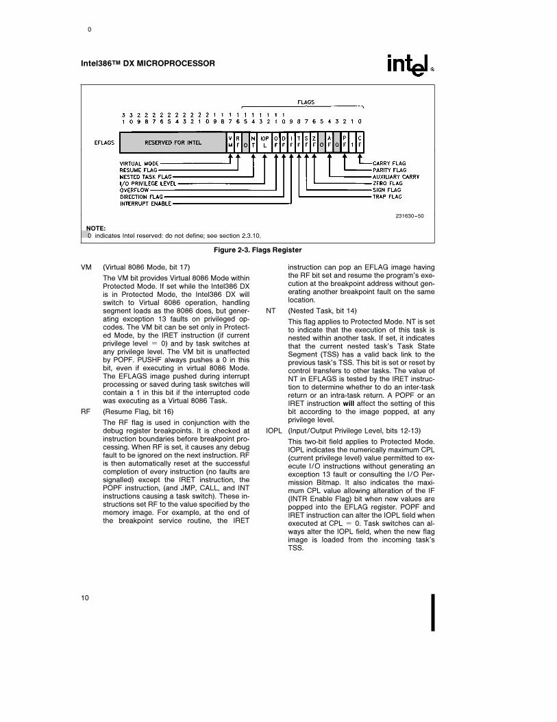
2.3.3 Flags Register
The Flags Register is a 32-bit register namedEFLAGS. The defined bits and bit fields withinEFLAGS, shown in Figure 2-3, control certain opera-tions and indicate status of the Intel386 DX. Thelower 16 bits (bit 0–15) of EFLAGS contain the16-bit flag register named FLAGS, which is mostuseful when executing 8086 and 80286 code.
9
0
Intel386TM DX MICROPROCESSOR
231630–50
NOTE:0 indicates Intel reserved: do not define; see section 2.3.10.
Figure 2-3. Flags Register
VM (Virtual 8086 Mode, bit 17)
The VM bit provides Virtual 8086 Mode withinProtected Mode. If set while the Intel386 DXis in Protected Mode, the Intel386 DX willswitch to Virtual 8086 operation, handlingsegment loads as the 8086 does, but gener-ating exception 13 faults on privileged op-codes. The VM bit can be set only in Protect-ed Mode, by the IRET instruction (if currentprivilege level e 0) and by task switches atany privilege level. The VM bit is unaffectedby POPF. PUSHF always pushes a 0 in thisbit, even if executing in virtual 8086 Mode.The EFLAGS image pushed during interruptprocessing or saved during task switches willcontain a 1 in this bit if the interrupted codewas executing as a Virtual 8086 Task.
RF (Resume Flag, bit 16)
The RF flag is used in conjunction with thedebug register breakpoints. It is checked atinstruction boundaries before breakpoint pro-cessing. When RF is set, it causes any debugfault to be ignored on the next instruction. RFis then automatically reset at the successfulcompletion of every instruction (no faults aresignalled) except the IRET instruction, thePOPF instruction, (and JMP, CALL, and INTinstructions causing a task switch). These in-structions set RF to the value specified by thememory image. For example, at the end ofthe breakpoint service routine, the IRET
instruction can pop an EFLAG image havingthe RF bit set and resume the program’s exe-cution at the breakpoint address without gen-erating another breakpoint fault on the samelocation.
NT (Nested Task, bit 14)
This flag applies to Protected Mode. NT is setto indicate that the execution of this task isnested within another task. If set, it indicatesthat the current nested task’s Task StateSegment (TSS) has a valid back link to theprevious task’s TSS. This bit is set or reset bycontrol transfers to other tasks. The value ofNT in EFLAGS is tested by the IRET instruc-tion to determine whether to do an inter-taskreturn or an intra-task return. A POPF or anIRET instruction will affect the setting of thisbit according to the image popped, at anyprivilege level.
IOPL (Input/Output Privilege Level, bits 12-13)
This two-bit field applies to Protected Mode.IOPL indicates the numerically maximum CPL(current privilege level) value permitted to ex-ecute I/O instructions without generating anexception 13 fault or consulting the I/O Per-mission Bitmap. It also indicates the maxi-mum CPL value allowing alteration of the IF(INTR Enable Flag) bit when new values arepopped into the EFLAG register. POPF andIRET instruction can alter the IOPL field whenexecuted at CPL e 0. Task switches can al-ways alter the IOPL field, when the new flagimage is loaded from the incoming task’sTSS.
10
Intel386TM DX MICROPROCESSOR
OF (Overflow Flag, bit 11)
OF is set if the operation resulted in a signedoverflow. Signed overflow occurs when theoperation resulted in carry/borrow into thesign bit (high-order bit) of the result but didnot result in a carry/borrow out of the high-order bit, or vice-versa. For 8/16/32 bit oper-ations, OF is set according to overflow at bit7/15/31, respectively.
DF (Direction Flag, bit 10)
DF defines whether ESI and/or EDI registerspostdecrement or postincrement during thestring instructions. Postincrement occurs ifDF is reset. Postdecrement occurs if DF isset.
IF (INTR Enable Flag, bit 9)
The IF flag, when set, allows recognition ofexternal interrupts signalled on the INTR pin.When IF is reset, external interrupts signalledon the INTR are not recognized. IOPL indi-cates the maximum CPL value allowing alter-ation of the IF bit when new values arepopped into EFLAGS or FLAGS.
TF (Trap Enable Flag, bit 8)
TF controls the generation of exception 1trap when single-stepping through code.When TF is set, the Intel386 DX generates anexception 1 trap after the next instruction isexecuted. When TF is reset, exception 1traps occur only as a function of the break-point addresses loaded into debug registersDR0–DR3.
SF (Sign Flag, bit 7)
SF is set if the high-order bit of the result isset, it is reset otherwise. For 8-, 16-, 32-bitoperations, SF reflects the state of bit 7, 15,31 respectively.
ZF (Zero Flag, bit 6)
ZF is set if all bits of the result are 0. Other-wise it is reset.
AF (Auxiliary Carry Flag, bit 4)
The Auxiliary Flag is used to simplify the addi-tion and subtraction of packed BCD quanti-ties. AF is set if the operation resulted in acarry out of bit 3 (addition) or a borrow into bit3 (subtraction). Otherwise AF is reset. AF isaffected by carry out of, or borrow into bit 3only, regardless of overall operand length: 8,16 or 32 bits.
PF (Parity Flags, bit 2)
PF is set if the low-order eight bits of the op-eration contains an even number of ‘‘1’s’’(even parity). PF is reset if the low-order eightbits have odd parity. PF is a function of onlythe low-order eight bits, regardless of oper-and size.
CF (Carry Flag, bit 0)
CF is set if the operation resulted in a carryout of (addition), or a borrow into (subtraction)the high-order bit. Otherwise CF is reset. For8-, 16- or 32-bit operations, CF is set accord-ing to carry/borrow at bit 7, 15 or 31, respec-tively.
Note in these descriptions, ‘‘set’’ means ‘‘set to 1,’’and ‘‘reset’’ means ‘‘reset to 0.’’
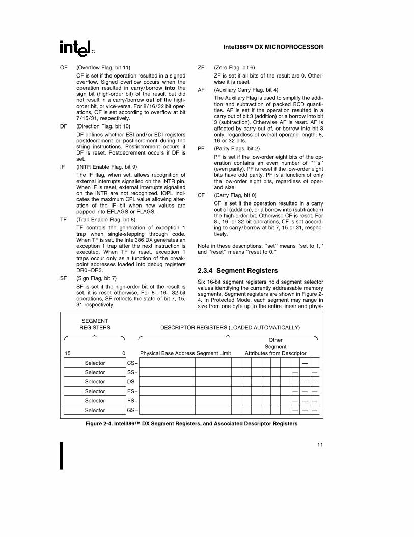
2.3.4 Segment Registers
Six 16-bit segment registers hold segment selectorvalues identifying the currently addressable memorysegments. Segment registers are shown in Figure 2-4. In Protected Mode, each segment may range insize from one byte up to the entire linear and physi-
SEGMENT
REGISTERS DESCRIPTOR REGISTERS (LOADED AUTOMATICALLY)V â W V â WOther
Segment
15 0 Physical Base Address Segment Limit Attributes from Descriptor
Selector CS– Ð
Selector SS– Ð Ð
Selector DS– Ð Ð Ð
Selector ES– Ð Ð Ð
Selector FS– Ð Ð Ð
Selector GS– Ð Ð Ð
Figure 2-4. Intel386TM DX Segment Registers, and Associated Descriptor Registers
11

Intel386TM DX MICROPROCESSOR
cal space of the machine, 4 Gbytes (232 bytes). If amaximum sized segment is used (limit e
FFFFFFFFH) it should be Dword aligned (i.e., theleast two significant bits of the segment base shouldbe zero). This will avoid a segment limit violation (ex-ception 13) caused by the wrap around. In Real Ad-dress Mode, the maximum segment size is fixed at64 Kbytes (216 bytes).
The six segments addressable at any given momentare defined by the segment registers CS, SS, DS,ES, FS and GS. The selector in CS indicates thecurrent code segment; the selector in SS indicatesthe current stack segment; the selectors in DS, ES,FS and GS indicate the current data segments.
2.3.5 Segment Descriptor Registers
The segment descriptor registers are not program-mer visible, yet it is very useful to understand theircontent. Inside the Intel386 DX, a descriptor register(programmer invisible) is associated with each pro-grammer-visible segment register, as shown by Fig-ure 2-4. Each descriptor register holds a 32-bit seg-ment base address, a 32-bit segment limit, and theother necessary segment attributes.
When a selector value is loaded into a segment reg-ister, the associated descriptor register is automati-cally updated with the correct information. In RealAddress Mode, only the base address is updateddirectly (by shifting the selector value four bits to theleft), since the segment maximum limit and attributesare fixed in Real Mode. In Protected Mode, the baseaddress, the limit, and the attributes are all updatedper the contents of the segment descriptor indexedby the selector.
Whenever a memory reference occurs, the segmentdescriptor register associated with the segment be-ing used is automatically involved with the memoryreference. The 32-bit segment base address be-comes a component of the linear address calcula-
tion, the 32-bit limit is used for the limit-check opera-tion, and the attributes are checked against the typeof memory reference requested.
2.3.6 Control Registers
The Intel386 DX has three control registers of 32bits, CR0, CR2 and CR3, to hold machine state of aglobal nature (not specific to an individual task).These registers, along with System Address Regis-ters described in the next section, hold machinestate that affects all tasks in the system. To accessthe Control Registers, load and store instructionsare defined.
CR0: Machine Control Register (includes 80286Machine Status Word)
CR0, shown in Figure 2-5, contains 6 defined bits forcontrol and status purposes. The low-order 16 bitsof CR0 are also known as the Machine Status Word,MSW, for compatibility with 80286 Protected Mode.LMSW and SMSW instructions are taken as specialaliases of the load and store CR0 operations, whereonly the low-order 16 bits of CR0 are involved. Forcompatibility with 80286 operating systems the In-tel386 DX LMSW instructions work in an identicalfashion to the LMSW instruction on the 80286. (i.e. Itonly operates on the low-order 16-bits of CR0 and itignores the new bits in CR0.) New Intel386 DX oper-ating systems should use the MOV CR0, Reg in-struction.
The defined CR0 bits are described below.
PG (Paging Enable, bit 31)
the PG bit is set to enable the on-chip pagingunit. It is reset to disable the on-chip pagingunit.
R (reserved, bit 4)
This bit is reserved by Intel. When loading CR0care should be taken to not alter the value ofthis bit.
31 24 23 16 15 8 7 0
P0 0 0 0 0 0 0 0 0 0 0 0 0 0 0 0 0 0 0 0 0 0 0 0 0 0 R
T E M PCR0
G S M P E
X ä YMSW
NOTE: 0 indicates Intel reserved: Do not define; SEE SECTION 2.3.10
Figure 2-5. Control Register 0
12

Intel386TM DX MICROPROCESSOR
TS (Task Switched, bit 3)
TS is automatically set whenever a task switchoperation is performed. If TS is set, a coproces-sor ESCape opcode will cause a CoprocessorNot Available trap (exception 7). The trap han-dler typically saves the Intel387 DX coproces-sor context belonging to a previous task, loadsthe Intel387 DX coprocessor state belonging tothe current task, and clears the TS bit beforereturning to the faulting coprocessor opcode.
EM (Emulate Coprocessor, bit 2)
The EMulate coprocessor bit is set to cause allcoprocessor opcodes to generate a Coproces-sor Not Available fault (exception 7). It is resetto allow coprocessor opcodes to be executedon an actual Intel387 DX coprocessor (this isthe default case after reset). Note that theWAIT opcode is not affected by the EM bit set-ting.
MP (Monitor Coprocessor, bit 1)
The MP bit is used in conjunction with the TSbit to determine if the WAIT opcode will gener-ate a Coprocessor Not Available fault (excep-tion 7) when TS e 1. When both MP e 1 andTS e 1, the WAIT opcode generates a trap.Otherwise, the WAIT opcode does not gener-ate a trap. Note that TS is automatically setwhenever a task switch operation is performed.
PE (Protection Enable, bit 0)
The PE bit is set to enable the Protected Mode.If PE is reset, the processor operates again inReal Mode. PE may be set by loading MSW orCR0. PE can be reset only by a load into CR0.Resetting the PE bit is typically part of a longerinstruction sequence needed for proper tran-sition from Protected Mode to Real Mode. Notethat for strict 80286 compatibility, PE cannot bereset by the LMSW instruction.
CR1: reserved
CR1 is reserved for use in future Intel processors.
CR2: Page Fault Linear Address
CR2, shown in Figure 2-6, holds the 32-bit linear ad-dress that caused the last page fault detected. The
error code pushed onto the page fault handler’sstack when it is invoked provides additional statusinformation on this page fault.
CR3: Page Directory Base Address
CR3, shown in Figure 2-6, contains the physicalbase address of the page directory table. The In-tel386 DX page directory table is always page-aligned (4 Kbyte-aligned). Therefore the lowesttwelve bits of CR3 are ignored when written andthey store as undefined.
A task switch through a TSS which changes thevalue in CR3, or an explicit load into CR3 with anyvalue, will invalidate all cached page table entries inthe paging unit cache. Note that if the value in CR3does not change during the task switch, the cachedpage table entries are not flushed.
2.3.7 System Address Registers
Four special registers are defined to reference thetables or segments supported by the 80286 CPUand Intel386 DX protection model. These tables orsegments are:
GDT (Global Descriptor Table),
IDT (Interrupt Descriptor Table),
LDT (Local Descriptor Table),
TSS (Task State Segment).
The addresses of these tables and segments arestored in special registers, the System Address andSystem Segment Registers illustrated in Figure 2-7.These registers are named GDTR, IDTR, LDTR andTR, respectively. Section 4 Protected Mode Archi-tecture describes the use of these registers.
GDTR and IDTR
These registers hold the 32-bit linear base addressand 16-bit limit of the GDT and IDT, respectively.
The GDT and IDT segments, since they are global toall tasks in the system, are defined by 32-bit linearaddresses (subject to page translation if paging isenabled) and 16-bit limit values.
31 24 23 16 15 8 7 0
PAGE FAULT LINEAR ADDRESS REGISTER CR2
PAGE DIRECTORY BASE REGISTER 0 0 0 0 0 0 0 0 0 0 0 0 CR3
NOTE: 0 indicates Intel reserved: Do not define; SEE SECTION 2.3.10
Figure 2-6. Control Registers 2 and 3
13

Intel386TM DX MICROPROCESSOR
SYSTEM ADDRESS REGISTERS
47 32-BIT LINEAR BASE ADDRESS 16 15 LIMIT 0
GDTR
IDTR
SYSTEM SEGMENT
REGISTERS DESCRIPTOR REGISTERS (AUTOMATICALLY LOADED)V â W V â W15 0 32-BIT LINEAR BASE ADDRESS 32-BIT SEGMENT LIMIT ATTRIBUTES
TR SELECTOR
LDTR SELECTOR
Figure 2-7. System Address and System Segment Registers
LDTR and TR
These registers hold the 16-bit selector for the LDTdescriptor and the TSS descriptor, respectively.
The LDT and TSS segments, since they are task-specific segments, are defined by selector valuesstored in the system segment registers. Note that asegment descriptor register (programmer-invisible)is associated with each system segment register.
2.3.8 Debug and Test Registers
Debug Registers: The six programmer accessibledebug registers provide on-chip support for debug-ging. Debug Registers DR0–3 specify the four linearbreakpoints. The Debug Control Register DR7 isused to set the breakpoints and the Debug StatusRegister DR6, displays the current state of thebreakpoints. The use of the debug registers is de-scribed in section 2.12 Debugging support.
DEBUG REGISTERS31 0
LINEAR BREAKPOINT ADDRESS 0 DR0
LINEAR BREAKPOINT ADDRESS 1 DR1
LINEAR BREAKPOINT ADDRESS 2 DR2
LINEAR BREAKPOINT ADDRESS 3 DR3
Intel reserved. Do not define. DR4
Intel reserved. Do not define. DR5
BREAKPOINT STATUS DR6
BREAKPOINT CONTROL DR7
TEST REGISTERS (FOR PAGE CACHE)31 0
TEST CONTROL TR6
TEST STATUS TR7
Figure 2-8. Debug and Test Registers
Test Registers: Two registers are used to controlthe testing of the RAM/CAM (Content AddressableMemories) in the Translation Lookaside Buffer por-tion of the Intel386 DX. TR6 is the command testregister, and TR7 is the data register which containsthe data of the Translation Lookaside buffer test.Their use is discussed in section 2.11 Testability.
Figure 2-8 shows the Debug and Test registers.
2.3.9 Register Accessibility
There are a few differences regarding the accessibil-ity of the registers in Real and Protected Mode. Ta-ble 2-1 summarizes these differences. See Section4 Protected Mode Architecture for further details.
2.3.10 Compatibility
VERY IMPORTANT NOTE:COMPATIBILITY WITH FUTURE PROCESSORS
In the preceding register descriptions, note cer-tain Intel386 DX register bits are Intel reserved.When reserved bits are called out, treat them asfully undefined. This is essential for your soft-ware compatibility with future processors! Fol-low the guidelines below:
1) Do not depend on the states of any unde-fined bits when testing the values of definedregister bits. Mask them out when testing.
2) Do not depend on the states of any unde-fined bits when storing them to memory oranother register.
3) Do not depend on the ability to retain infor-mation written into any undefined bits.
4) When loading registers always load the unde-fined bits as zeros.
14
Intel386TM DX MICROPROCESSOR
Table 2-1. Register Usage
Use in Use in Use in
RegisterReal Mode Protected Mode Virtual 8086 Mode
Load Store Load Store Load Store
General Registers Yes Yes Yes Yes Yes Yes
Segment Registers Yes Yes Yes Yes Yes Yes
Flag Register Yes Yes Yes Yes IOPL* IOPL*
Control Registers Yes Yes PL e 0 PL e 0 No Yes
GDTR Yes Yes PL e 0 Yes No Yes
IDTR Yes Yes PL e 0 Yes No Yes
LDTR No No PL e 0 Yes No No
TR No No PL e 0 Yes No No
Debug Control Yes Yes PL e 0 PL e 0 No No
Test Registers Yes Yes PL e 0 PL e 0 No No
NOTES:PL e 0: The registers can be accessed only when the current privilege level is zero.*IOPL: The PUSHF and POPF instructions are made I/O Privilege Level sensitive in Virtual 8086 Mode.
5) However, registers which have been previ-ously stored may be reloaded without mask-ing.
Depending upon the values of undefined regis-ter bits will make your software dependent uponthe unspecified Intel386 DX handling of thesebits. Depending on undefined values risks mak-ing your software incompatible with future proc-essors that define usages for the Intel386 DX-undefined bits. AVOID ANY SOFTWARE DEPEN-DENCE UPON THE STATE OF UNDEFINED In-tel386 DX REGISTER BITS.
2.4 INSTRUCTION SET
2.4.1 Instruction Set Overview
The instruction set is divided into nine categories ofoperations:
Data Transfer
Arithmetic
Shift/Rotate
String Manipulation
Bit Manipulation
Control Transfer
High Level Language Support
Operating System Support
Processor Control
These Intel386 DX instructions are listed in Table2-2.
All Intel386 DX instructions operate on either 0, 1, 2,or 3 operands; where an operand resides in a regis-ter, in the instruction itself, or in memory. Most zerooperand instructions (e.g. CLI, STI) take only onebyte. One operand instructions generally are twobytes long. The average instruction is 3.2 bytes long.Since the Intel386 DX has a 16-byte instructionqueue, an average of 5 instructions will be pre-fetched. The use of two operands permits the follow-ing types of common instructions:
Register to Register
Memory to Register
Immediate to Register
Register to Memory
Immediate to Memory.
The operands can be either 8, 16, or 32 bits long. Asa general rule, when executing code written for theIntel386 DX (32-bit code), operands are 8 or 32 bits;when executing existing 80286 or 8086 code (16-bitcode), operands are 8 or 16 bits. Prefixes can beadded to all instructions which override the defaultlength of the operands, (i.e. use 32-bit operands for16-bit code, or 16-bit operands for 32-bit code).
For a more elaborate description of the instructionset, refer to the Intel386 DX Programmer’s Refer-ence Manual.
15
Intel386TM DX MICROPROCESSOR
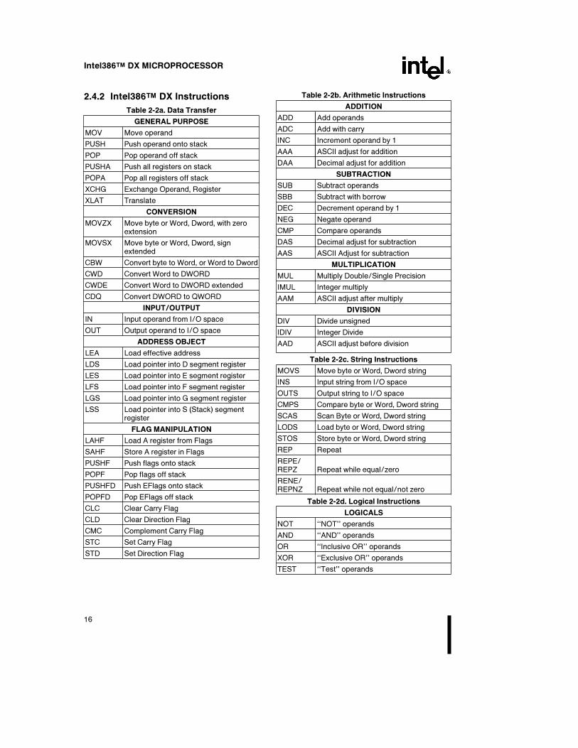
2.4.2 Intel386TM DX Instructions
Table 2-2a. Data Transfer
GENERAL PURPOSE
MOV Move operand
PUSH Push operand onto stack
POP Pop operand off stack
PUSHA Push all registers on stack
POPA Pop all registers off stack
XCHG Exchange Operand, Register
XLAT Translate
CONVERSION
MOVZX Move byte or Word, Dword, with zeroextension
MOVSX Move byte or Word, Dword, signextended
CBW Convert byte to Word, or Word to Dword
CWD Convert Word to DWORD
CWDE Convert Word to DWORD extended
CDQ Convert DWORD to QWORD
INPUT/OUTPUT
IN Input operand from I/O space
OUT Output operand to I/O space
ADDRESS OBJECT
LEA Load effective address
LDS Load pointer into D segment register
LES Load pointer into E segment register
LFS Load pointer into F segment register
LGS Load pointer into G segment register
LSS Load pointer into S (Stack) segmentregister
FLAG MANIPULATION
LAHF Load A register from Flags
SAHF Store A register in Flags
PUSHF Push flags onto stack
POPF Pop flags off stack
PUSHFD Push EFlags onto stack
POPFD Pop EFlags off stack
CLC Clear Carry Flag
CLD Clear Direction Flag
CMC Complement Carry Flag
STC Set Carry Flag
STD Set Direction Flag
Table 2-2b. Arithmetic Instructions
ADDITION
ADD Add operands
ADC Add with carry
INC Increment operand by 1
AAA ASCII adjust for addition
DAA Decimal adjust for addition
SUBTRACTION
SUB Subtract operands
SBB Subtract with borrow
DEC Decrement operand by 1
NEG Negate operand
CMP Compare operands
DAS Decimal adjust for subtraction
AAS ASCII Adjust for subtraction
MULTIPLICATION
MUL Multiply Double/Single Precision
IMUL Integer multiply
AAM ASCII adjust after multiply
DIVISION
DIV Divide unsigned
IDIV Integer Divide
AAD ASCII adjust before division
Table 2-2c. String Instructions
MOVS Move byte or Word, Dword string
INS Input string from I/O space
OUTS Output string to I/O space
CMPS Compare byte or Word, Dword string
SCAS Scan Byte or Word, Dword string
LODS Load byte or Word, Dword string
STOS Store byte or Word, Dword string
REP Repeat
REPE/REPZ Repeat while equal/zero
RENE/REPNZ Repeat while not equal/not zero
Table 2-2d. Logical Instructions
LOGICALS
NOT ‘‘NOT’’ operands
AND ‘‘AND’’ operands
OR ‘‘Inclusive OR’’ operands
XOR ‘‘Exclusive OR’’ operands
TEST ‘‘Test’’ operands
16

Intel386TM DX MICROPROCESSOR
Table 2-2d. Logical Instructions (Continued)
SHIFTS
SHL/SHR Shift logical left or right
SAL/SAR Shift arithmetic left or right
SHLD/SHRD Double shift left or right
ROTATES
ROL/ROR Rotate left/right
RCL/RCR Rotate through carry left/right
Table 2-2e. Bit Manipulation Instructions
SINGLE BIT INSTRUCTIONS
BT Bit Test
BTS Bit Test and Set
BTR Bit Test and Reset
BTC Bit Test and Complement
BSF Bit Scan Forward
BSR Bit Scan Reverse
Table 2-2f. Program Control Instructions
CONDITIONAL TRANSFERS
SETCC Set byte equal to condition code
JA/JNBE Jump if above/not below nor equal
JAE/JNB Jump if above or equal/not below
JB/JNAE Jump if below/not above nor equal
JBE/JNA Jump if below or equal/not above
JC Jump if carry
JE/JZ Jump if equal/zero
JG/JNLE Jump if greater/not less nor equal
JGE/JNL Jump if greater or equal/not less
JL/JNGE Jump if less/not greater nor equal
JLE/JNG Jump if less or equal/not greater
JNC Jump if not carry
JNE/JNZ Jump if not equal/not zero
JNO Jump if not overflow
JNP/JPO Jump if not parity/parity odd
JNS Jump if not sign
JO Jump if overflow
JP/JPE Jump if parity/parity even
JS Jump if Sign
Table 2-2f. Program Control Instructions
(Continued)
UNCONDITIONAL TRANSFERS
CALL Call procedure/task
RET Return from procedure
JMP Jump
ITERATION CONTROLS
LOOP Loop
LOOPE/LOOPZ Loop if equal/zero
LOOPNE/LOOPNZ Loop if not equal/not zero
JCXZ JUMP if register CXe0
INTERRUPTS
INT Interrupt
INTO Interrupt if overflow
IRET Return from Interrupt/Task
CLI Clear interrupt Enable
STI Set Interrupt Enable
Table 2-2g. High Level Language Instructions
BOUND Check Array Bounds
ENTER Setup Parameter Block for EnteringProcedure
LEAVE Leave Procedure
Table 2-2h. Protection Model
SGDT Store Global Descriptor Table
SIDT Store Interrupt Descriptor Table
STR Store Task Register
SLDT Store Local Descriptor Table
LGDT Load Global Descriptor Table
LIDT Load Interrupt Descriptor Table
LTR Load Task Register
LLDT Load Local Descriptor Table
ARPL Adjust Requested Privilege Level
LAR Load Access Rights
LSL Load Segment Limit
VERR/VERW Verify Segment for Reading or Writing
LMSW Load Machine Status Word (lower16 bits of CR0)
SMSW Store Machine Status Word
Table 2-2i. Processor Control Instructions
HLT Halt
WAIT Wait until BUSYÝ negated
ESC Escape
LOCK Lock Bus
17

Intel386TM DX MICROPROCESSOR
2.5 ADDRESSING MODES
2.5.1 Addressing Modes Overview
The Intel386 DX provides a total of 11 addressingmodes for instructions to specify operands. The ad-dressing modes are optimized to allow the efficientexecution of high level languages such as C andFORTRAN, and they cover the vast majority of datareferences needed by high-level languages.
2.5.2 Register and Immediate Modes
Two of the addressing modes provide for instruc-tions that operate on register or immediate oper-ands:
Register Operand Mode: The operand is locatedin one of the 8-, 16- or 32-bit general registers.
Immediate Operand Mode: The operand is in-cluded in the instruction as part of the opcode.
2.5.3 32-Bit Memory AddressingModes
The remaining 9 modes provide a mechanism forspecifying the effective address of an operand. Thelinear address consists of two components: the seg-ment base address and an effective address. Theeffective address is calculated by using combina-tions of the following four address elements:
DISPLACEMENT: An 8-, or 32-bit immediate value,following the instruction.
BASE: The contents of any general purpose regis-ter. The base registers are generally used by compil-ers to point to the start of the local variable area.
INDEX: The contents of any general purpose regis-ter except for ESP. The index registers are used toaccess the elements of an array, or a string of char-acters.
SCALE: The index register’s value can be multipliedby a scale factor, either 1, 2, 4 or 8. Scaled indexmode is especially useful for accessing arrays orstructures.
Combinations of these 4 components make up the 9additional addressing modes. There is no perform-ance penalty for using any of these addressing com-binations, since the effective address calculation ispipelined with the execution of other instructions.
The one exception is the simultaneous use of Baseand Index components which requires one addition-al clock.
As shown in Figure 2-9, the effective address (EA) ofan operand is calculated according to the followingformula.
EAeBase Rega(Index Reg * Scaling)aDisplacement
Direct Mode: The operand’s offset is contained aspart of the instruction as an 8-, 16- or 32-bit dis-placement.EXAMPLE: INC Word PTR [500]
Register Indirect Mode: A BASE register containsthe address of the operand.EXAMPLE: MOV [ECX], EDX
Based Mode: A BASE register’s contents is addedto a DISPLACEMENT to form the operands offset.EXAMPLE: MOV ECX, [EAXa24]
Index Mode: An INDEX register’s contents is addedto a DISPLACEMENT to form the operands offset.EXAMPLE: ADD EAX, TABLE[ESI]
Scaled Index Mode: An INDEX register’s contents ismultiplied by a scaling factor which is added to aDISPLACEMENT to form the operands offset.EXAMPLE: IMUL EBX, TABLE[ESI*4],7
Based Index Mode: The contents of a BASE registeris added to the contents of an INDEX register toform the effective address of an operand.EXAMPLE: MOV EAX, [ESI] [EBX]
Based Scaled Index Mode: The contents of an IN-DEX register is multiplied by a SCALING factor andthe result is added to the contents of a BASE regis-ter to obtain the operands offset.EXAMPLE: MOV ECX, [EDX*8] [EAX]
Based Index Mode with Displacement: The contentsof an INDEX Register and a BASE register’s con-tents and a DISPLACEMENT are all summed to-gether to form the operand offset.EXAMPLE: ADD EDX, [ESI] [EBPa00FFFFF0H]
Based Scaled Index Mode with Displacement: Thecontents of an INDEX register are multiplied by aSCALING factor, the result is added to the contentsof a BASE register and a DISPLACEMENT to formthe operand’s offset.EXAMPLE: MOV EAX, LOCALTABLE[EDI*4][EBPa80]
18

Intel386TM DX MICROPROCESSOR
231630–51
Figure 2-9. Addressing Mode Calculations
2.5.4 Differences Between 16 and 32Bit Addresses
In order to provide software compatibility with the80286 and the 8086, the Intel386 DX can execute16-bit instructions in Real and Protected Modes. Theprocessor determines the size of the instructions it isexecuting by examining the D bit in the CS segmentDescriptor. If the D bit is 0 then all operand lengthsand effective addresses are assumed to be 16 bitslong. If the D bit is 1 then the default length for oper-ands and addresses is 32 bits. In Real Mode thedefault size for operands and addresses is 16-bits.
Regardless of the default precision of the operandsor addresses, the Intel386 DX is able to execute ei-ther 16 or 32-bit instructions. This is specified via theuse of override prefixes. Two prefixes, the OperandSize Prefix and the Address Length Prefix, over-ride the value of the D bit on an individual instructionbasis. These prefixes are automatically added by In-tel assemblers.
Example: The processor is executing in Real Modeand the programmer needs to access the EAX regis-ters. The assembler code for this might be MOVEAX, 32-bit MEMORYOP, ASM386 Macro Assem-bler automatically determines that an Operand SizePrefix is needed and generates it.
Example: The D bit is 0, and the programmer wishesto use Scaled Index addressing mode to access anarray. The Address Length Prefix allows the use ofMOV DX, TABLE[ESI*2]. The assembler uses anAddress Length Prefix since, with De0, the defaultaddressing mode is 16-bits.
Example: The D bit is 1, and the program wants tostore a 16-bit quantity. The Operand Length Prefix isused to specify only a 16-bit value; MOV MEM16,DX.
19
Intel386TM DX MICROPROCESSOR
Table 2-3. BASE and INDEX Registers for 16- and 32-Bit Addresses
16-Bit Addressing 32-Bit Addressing
BASE REGISTER BX,BP Any 32-bit GP Register
INDEX REGISTER SI,DI Any 32-bit GP Register
Except ESP
SCALE FACTOR none 1, 2, 4, 8
DISPLACEMENT 0, 8, 16 bits 0, 8, 32 bits
The OPERAND LENGTH and Address Length Pre-fixes can be applied separately or in combination toany instruction. The Address Length Prefix does notallow addresses over 64K bytes to be accessed inReal Mode. A memory address which exceedsFFFFH will result in a General Protection Fault. AnAddress Length Prefix only allows the use of the ad-ditional Intel386 DX addressing modes.
When executing 32-bit code, the Intel386 DX useseither 8-, or 32-bit displacements, and any registercan be used as base or index registers. When exe-cuting 16-bit code, the displacements are either 8, or16 bits, and the base and index register conform tothe 80286 model. Table 2-3 illustrates the differenc-es.
2.6 DATA TYPES
The Intel386 DX supports all of the data types com-monly used in high level languages:
Bit: A single bit quantity.
Bit Field: A group of up to 32 contiguous bits,which spans a maximum of four bytes.
Bit String: A set of contiguous bits, on the Intel386DX bit strings can be up to 4 gigabits long.
Byte: A signed 8-bit quantity.
Unsigned Byte: An unsigned 8-bit quantity.
Integer (Word): A signed 16-bit quantity.
Long Integer (Double Word): A signed 32-bit quan-tity. All operations assume a 2’s complement rep-resentation.
Unsigned Integer (Word): An unsigned 16-bitquantity.
Unsigned Long Integer (Double Word): An un-signed 32-bit quantity.
Signed Quad Word: A signed 64-bit quantity.
Unsigned Quad Word: An unsigned 64-bit quanti-ty.
Offset: A 16- or 32-bit offset only quantity whichindirectly references another memory location.
Pointer: A full pointer which consists of a 16-bitsegment selector and either a 16- or 32-bit offset.
Char: A byte representation of an ASCII Alphanu-meric or control character.
String: A contiguous sequence of bytes, words ordwords. A string may contain between 1 byte and4 Gbytes.
BCD: A byte (unpacked) representation of decimaldigits 0–9.
Packed BCD: A byte (packed) representation oftwo decimal digits 0–9 storing one digit in eachnibble.
When the Intel386 DX is coupled with an Intel387DX Numerics Coprocessor then the following com-mon Floating Point types are supported.
Floating Point: A signed 32-, 64-, or 80-bit realnumber representation. Floating point numbersare supported by the Intel387 DX numerics co-processor.
Figure 2-10 illustrates the data types supported bythe Intel386 DX and the Intel387 DX numerics co-processor.
20

Intel386TM DX MICROPROCESSOR
231630–52
Figure 2-10. Intel386TM DX Supported Data Types
21

Intel386TM DX MICROPROCESSOR
2.7 MEMORY ORGANIZATION
2.7.1 Introduction
Memory on the Intel386 DX is divided up into 8-bitquantities (bytes), 16-bit quantities (words), and32-bit quantities (dwords). Words are stored in twoconsecutive bytes in memory with the low-order byteat the lowest address, the high order byte at the highaddress. Dwords are stored in four consecutivebytes in memory with the low-order byte at the low-est address, the high-order byte at the highest ad-dress. The address of a word or dword is the byteaddress of the low-order byte.
In addition to these basic data types, the Intel386DX supports two larger units of memory: pages andsegments. Memory can be divided up into one ormore variable length segments, which can beswapped to disk or shared between programs. Mem-ory can also be organized into one or more 4K bytepages. Finally, both segmentation and paging canbe combined, gaining the advantages of both sys-tems. The Intel386 DX supports both pages andsegments in order to provide maximum flexibility tothe system designer. Segmentation and paging arecomplementary. Segmentation is useful for organiz-ing memory in logical modules, and as such is a toolfor the application programmer, while pages are use-ful for the system programmer for managing thephysical memory of a system.
2.7.2 Address Spaces
The Intel386 DX has three distinct address spaces:logical, linear, and physical. A logical address
(also known as a virtual address) consists of a se-lector and an offset. A selector is the contents of asegment register. An offset is formed by summing allof the addressing components (BASE, INDEX, DIS-PLACEMENT) discussed in section 2.5.3 MemoryAddressing Modes into an effective address. Sinceeach task on Intel386 DX has a maximum of 16K(214 b1) selectors, and offsets can be 4 gigabytes,(232 bits) this gives a total of 246 bits or 64 terabytesof logical address space per task. The programmersees this virtual address space.
The segmentation unit translates the logical ad-dress space into a 32-bit linear address space. If thepaging unit is not enabled then the 32-bit linear ad-dress corresponds to the physical address. Thepaging unit translates the linear address space intothe physical address space. The physical addressis what appears on the address pins.
The primary difference between Real Mode and Pro-tected Mode is how the segmentation unit performsthe translation of the logical address into the linearaddress. In Real Mode, the segmentation unit shiftsthe selector left four bits and adds the result to theoffset to form the linear address. While in ProtectedMode every selector has a linear base address as-sociated with it. The linear base address is stored inone of two operating system tables (i.e. the LocalDescriptor Table or Global Descriptor Table). Theselector’s linear base address is added to the offsetto form the final linear address.
Figure 2-11 shows the relationship between the vari-ous address spaces.
231630–53
Figure 2-11. Address Translation
22
Intel386TM DX MICROPROCESSOR
2.7.3 Segment Register Usage
The main data structure used to organize memory isthe segment. On the Intel386 DX, segments are vari-able sized blocks of linear addresses which havecertain attributes associated with them. There aretwo main types of segments: code and data, thesegments are of variable size and can be as smallas 1 byte or as large as 4 gigabytes (232 bytes).
In order to provide compact instruction encoding,and increase processor performance, instructionsdo not need to explicitly specify which segment reg-ister is used. A default segment register is automati-cally chosen according to the rules of Table 2-4(Segment Register Selection Rules). In general, datareferences use the selector contained in the DS reg-ister; Stack references use the SS register and In-struction fetches use the CS register. The contentsof the Instruction Pointer provides the offset. Specialsegment override prefixes allow the explicit use of agiven segment register, and override the implicitrules listed in Table 2-4. The override prefixes alsoallow the use of the ES, FS and GS segment regis-ters.
There are no restrictions regarding the overlappingof the base addresses of any segments. Thus, all 6segments could have the base address set to zeroand create a system with a four gigabyte linear ad-dress space. This creates a system where the virtualaddress space is the same as the linear addressspace. Further details of segmentation are dis-cussed in section 4.1.
2.8 I/O SPACE
The Intel386 DX has two distinct physical addressspaces: Memory and I/O. Generally, peripherals areplaced in I/O space although the Intel386 DX alsosupports memory-mapped peripherals. The I/Ospace consists of 64K bytes, it can be divided into64K 8-bit ports, 32K 16-bit ports, or 16K 32-bit ports,or any combination of ports which add up to lessthan 64K bytes. The 64K I/O address space refersto physical memory rather than linear address sinceI/O instructions do not go through the segmentationor paging hardware. The M/IOÝ pin acts as an addi-tional address line thus allowing the system designerto easily determine which address space the proces-sor is accessing.
Table 2-4. Segment Register Selection Rules
Type of Implied (Default) Segment Override
Memory Reference Segment Use Prefixes Possible
Code Fetch CS None
Destination of PUSH, PUSHF, INT, SS NoneCALL, PUSHA Instructions
Source of POP, POPA, POPF, SS NoneIRET, RET instructions
Destination of STOS, MOVS, REP ES NoneSTOS, REP MOVS Instructions(DI is Base Register)
Other Data References, withEffective Address Using BaseRegister of:
[EAX] DS DS,CS,SS,ES,FS,GS[EBX] DS DS,CS,SS,ES,FS,GS[ECX] DS DS,CS,SS,ES,FS,GS[EDX] DS DS,CS,SS,ES,FS,GS[ESI] DS DS,CS,SS,ES,FS,GS[EDI] DS DS,CS,SS,ES,FS,GS[EBP] SS DS,CS,SS,ES,FS,GS[ESP] SS DS,CS,SS,ES,FS,GS
23
Intel386TM DX MICROPROCESSOR
The I/O ports are accessed via the IN and OUT I/Oinstructions, with the port address supplied as animmediate 8-bit constant in the instruction or in theDX register. All 8- and 16-bit port addresses are zeroextended on the upper address lines. The I/O in-structions cause the M/IOÝ pin to be driven low.
I/O port addresses 00F8H through 00FFH are re-served for use by Intel.
2.9 INTERRUPTS
2.9.1 Interrupts and Exceptions
Interrupts and exceptions alter the normal programflow, in order to handle external events, to reporterrors or exceptional conditions. The difference be-tween interrupts and exceptions is that interrupts areused to handle asynchronous external events whileexceptions handle instruction faults. Although a pro-gram can generate a software interrupt via an INT Ninstruction, the processor treats software interruptsas exceptions.
Hardware interrupts occur as the result of an exter-nal event and are classified into two types: maskableor non-maskable. Interrupts are serviced after theexecution of the current instruction. After the inter-rupt handler is finished servicing the interrupt, exe-cution proceeds with the instruction immediately af-ter the interrupted instruction. Sections 2.9.3 and2.9.4 discuss the differences between Maskable andNon-Maskable interrupts.
Exceptions are classified as faults, traps, or abortsdepending on the way they are reported, and wheth-er or not restart of the instruction causing the excep-tion is supported. Faults are exceptions that are de-tected and serviced before the execution of thefaulting instruction. A fault would occur in a virtualmemory system, when the processor referenced apage or a segment which was not present. The oper-ating system would fetch the page or segment fromdisk, and then the Intel386 DX would restart the in-struction. Traps are exceptions that are reported im-mediately after the execution of the instructionwhich caused the problem. User defined interruptsare examples of traps. Aborts are exceptions whichdo not permit the precise location of the instructioncausing the exception to be determined. Aborts areused to report severe errors, such as a hardwareerror, or illegal values in system tables.
Thus, when an interrupt service routine has beencompleted, execution proceeds from the instruction
immediately following the interrupted instruction. Onthe other hand, the return address from an excep-tion fault routine will always point at the instructioncausing the exception and include any leading in-struction prefixes. Table 2-5 summarizes the possi-ble interrupts for the Intel386 DX and shows wherethe return address points.
The Intel386 DX has the ability to handle up to 256different interrupts/exceptions. In order to servicethe interrupts, a table with up to 256 interrupt vec-tors must be defined. The interrupt vectors are sim-ply pointers to the appropriate interrupt service rou-tine. In Real Mode (see section 3.1), the vectors are4 byte quantities, a Code Segment plus a 16-bit off-set; in Protected Mode, the interrupt vectors are 8byte quantities, which are put in an Interrupt Descrip-tor Table (see section 4.1). Of the 256 possible inter-rupts, 32 are reserved for use by Intel, the remaining224 are free to be used by the system designer.
2.9.2 Interrupt Processing
When an interrupt occurs the following actions hap-pen. First, the current program address and theFlags are saved on the stack to allow resumption ofthe interrupted program. Next, an 8-bit vector is sup-plied to the Intel386 DX which identifies the appro-priate entry in the interrupt table. The table containsthe starting address of the interrupt service routine.Then, the user supplied interrupt service routine isexecuted. Finally, when an IRET instruction is exe-cuted the old processor state is restored and pro-gram execution resumes at the appropriate instruc-tion.
The 8-bit interrupt vector is supplied to the Intel386DX in several different ways: exceptions supply theinterrupt vector internally; software INT instructionscontain or imply the vector; maskable hardware in-terrupts supply the 8-bit vector via the interrupt ac-knowledge bus sequence. Non-Maskable hardwareinterrupts are assigned to interrupt vector 2.
2.9.3 Maskable Interrupt
Maskable interrupts are the most common way usedby the Intel386 DX to respond to asynchronous ex-ternal hardware events. A hardware interrupt occurswhen the INTR is pulled high and the Interrupt Flagbit (IF) is enabled. The processor only responds tointerrupts between instructions, (REPeat String in-structions, have an ‘‘interrupt window’’, betweenmemory moves, which allows interrupts during long
24

Intel386TM DX MICROPROCESSOR
Table 2-5. Interrupt Vector Assignments
Instruction WhichReturn Address
FunctionInterrupt
Can CausePoints to
TypeNumber
ExceptionFaulting
Instruction
Divide Error 0 DIV, IDIV YES FAULT
Debug Exception 1 any instruction YES TRAP*
NMI Interrupt 2 INT 2 or NMI NO NMI
One Byte Interrupt 3 INT NO TRAP
Interrupt on Overflow 4 INTO NO TRAP
Array Bounds Check 5 BOUND YES FAULT
Invalid OP-Code 6 Any Illegal Instruction YES FAULT
Device Not Available 7 ESC, WAIT YES FAULT
Double Fault 8 Any Instruction That Can ABORTGenerate an Exception
Coprocessor Segment Overrun 9 ESC NO ABORT
Invalid TSS 10 JMP, CALL, IRET, INT YES FAULT
Segment Not Present 11 Segment Register Instructions YES FAULT
Stack Fault 12 Stack References YES FAULT
General Protection Fault 13 Any Memory Reference YES FAULT
Intel Reserved 15
Page Fault 14 Any Memory Access or Code Fetch YES FAULT
Coprocessor Error 16 ESC, WAIT YES FAULT
Intel Reserved 17–31
Two Byte Interrupt 0–255 INT n NO TRAP
* Some debug exceptions may report both traps on the previous instruction, and faults on the next instruction.
string moves). When an interrupt occurs the proces-sor reads an 8-bit vector supplied by the hardwarewhich identifies the source of the interrupt, (one of224 user defined interrupts). The exact nature of theinterrupt sequence is discussed in section 5.
The IF bit in the EFLAG registers is reset when aninterrupt is being serviced. This effectively disablesservicing additional interrupts during an interruptservice routine. However, the IF may be set explicitlyby the interrupt handler, to allow the nesting of inter-rupts. When an IRET instruction is executed theoriginal state of the IF is restored.
2.9.4 Non-Maskable Interrupt
Non-maskable interrupts provide a method of servic-ing very high priority interrupts. A common exampleof the use of a non-maskable interrupt (NMI) wouldbe to activate a power failure routine. When the NMI
input is pulled high it causes an interrupt with aninternally supplied vector value of 2. Unlike a normalhardware interrupt, no interrupt acknowledgment se-quence is performed for an NMI.
While executing the NMI servicing procedure, the In-tel386 DX will not service further NMI requests, untilan interrupt return (IRET) instruction is executed orthe processor is reset. If NMI occurs while currentlyservicing an NMI, its presence will be saved for serv-icing after executing the first IRET instruction. The IFbit is cleared at the beginning of an NMI interrupt toinhibit further INTR interrupts.
2.9.5 Software Interrupts
A third type of interrupt/exception for the Intel386DX is the software interrupt. An INT n instructioncauses the processor to execute the interrupt serv-ice routine pointed to by the nth vector in the inter-rupt table.
25

Intel386TM DX MICROPROCESSOR
A special case of the two byte software interrupt INTn is the one byte INT 3, or breakpoint interrupt. Byinserting this one byte instruction in a program, theuser can set breakpoints in his program as a debug-ging tool.
A final type of software interrupt, is the single stepinterrupt. It is discussed in section 2.12.
2.9.6 Interrupt and ExceptionPriorities
Interrupts are externally-generated events. Maska-ble Interrupts (on the INTR input) and Non-MaskableInterrupts (on the NMI input) are recognized at in-struction boundaries. When NMI and maskableINTR are both recognized at the same instructionboundary, the Intel386 DX invokes the NMI serviceroutine first. If, after the NMI service routine hasbeen invoked, maskable interrupts are still enabled,then the Intel386 DX will invoke the appropriate in-terrupt service routine.
Table 2-6a. Intel386TM DX Priority for
Invoking Service Routines in Case of
Simultaneous External Interrupts
1. NMI
2. INTR
Exceptions are internally-generated events. Excep-tions are detected by the Intel386 DX if, in thecourse of executing an instruction, the Intel386 DXdetects a problematic condition. The Intel386 DXthen immediately invokes the appropriate exceptionservice routine. The state of the Intel386 DX is suchthat the instruction causing the exception can be re-started. If the exception service routine has takencare of the problematic condition, the instruction willexecute without causing the same exception.
It is possible for a single instruction to generate sev-eral exceptions (for example, transferring a singleoperand could generate two page faults if the oper-and location spans two ‘‘not present’’ pages). How-ever, only one exception is generated upon each at-tempt to execute the instruction. Each exceptionservice routine should correct its corresponding ex-ception, and restart the instruction. In this manner,exceptions are serviced until the instruction exe-cutes successfully.
As the Intel386 DX executes instructions, it follows aconsistent cycle in checking for exceptions, asshown in Table 2-6b. This cycle is repeated
as each instruction is executed, and occurs in paral-lel with instruction decoding and execution.
Table 2-6b. Sequence of Exception Checking
Consider the case of the Intel386 DX having justcompleted an instruction. It then performs thefollowing checks before reaching the point wherethe next instruction is completed:
1. Check for Exception 1 Traps from the instruc-tion just completed (single-step via Trap Flag,or Data Breakpoints set in the Debug Regis-ters).
2. Check for Exception 1 Faults in the next in-struction (Instruction Execution Breakpoint setin the Debug Registers for the next instruc-tion).
3. Check for external NMI and INTR.
4. Check for Segmentation Faults that preventedfetching the entire next instruction (exceptions11 or 13).
5. Check for Page Faults that prevented fetchingthe entire next instruction (exception 14).
6. Check for Faults decoding the next instruction(exception 6 if illegal opcode; exception 6 if inReal Mode or in Virtual 8086 Mode and at-tempting to execute an instruction for Protect-ed Mode only (see 4.6.4); or exception 13 ifinstruction is longer than 15 bytes, or privilegeviolation in Protected Mode (i.e. not at IOPL orat CPLe0).
7. If WAIT opcode, check if TSe1 and MPe1(exception 7 if both are 1).
8. If ESCAPE opcode for numeric coprocessor,check if EMe1 or TSe1 (exception 7 if eitherare 1).
9. If WAIT opcode or ESCAPE opcode for nu-meric coprocessor, check ERRORÝ input sig-nal (exception 16 if ERRORÝ input is assert-ed).
10. Check in the following order for each memo-ry reference required by the instruction:
a. Check for Segmentation Faults that pre-vent transferring the entire memory quanti-ty (exceptions 11, 12, 13).
b. Check for Page Faults that prevent trans-ferring the entire memory quantity (excep-tion 14).
Note that the order stated supports the conceptof the paging mechanism being ‘‘underneath’’the segmentation mechanism. Therefore, for anygiven code or data reference in memory, seg-mentation exceptions are generated before pag-ing exceptions are generated.
26

Intel386TM DX MICROPROCESSOR
2.9.7 Instruction Restart
The Intel386 DX fully supports restarting all instruc-tions after faults. If an exception is detected in theinstruction to be executed (exception categories 4through 10 in Table 2-6b), the Intel386 DX invokesthe appropriate exception service routine. The In-tel386 DX is in a state that permits restart of theinstruction, for all cases but those in Table 2-6c.Note that all such cases are easily avoided by prop-er design of the operating system.
Table 2-6c. Conditions Preventing
Instruction Restart
A. An instruction causes a task switch to a taskwhose Task State Segment is partially ‘‘notpresent’’. (An entirely ‘‘not present’’ TSS is re-startable.) Partially present TSS’s can beavoided either by keeping the TSS’s of suchtasks present in memory, or by aligning TSSsegments to reside entirely within a single 4Kpage (for TSS segments of 4K bytes or less).
B. A coprocessor operand wraps around the topof a 64K-byte segment or a 4G-byte segment,and spans three pages, and the page holdingthe middle portion of the operand is ‘‘not pres-ent.’’ This condition can be avoided by startingat a page boundary any segments containingcoprocessor operands if the segments are ap-proximately 64K-200 bytes or larger (i.e. largeenough for wraparound of the coprocessoroperand to possibly occur).
Note that these conditions are avoided by usingthe operating system designs mentioned in thistable.
2.9.8 Double Fault
A Double Fault (exception 8) results when the proc-essor attempts to invoke an exception service rou-tine for the segment exceptions (10, 11, 12 or 13),but in the process of doing so, detects an exceptionother than a Page Fault (exception 14).
A Double Fault (exception 8) will also be generatedwhen the processor attempts to invoke the PageFault (exception 14) service routine, and detects anexception other than a second Page Fault. In anyfunctional system, the entire Page Fault service rou-tine must remain ‘‘present’’ in memory.
Double page faults however do not raise the doublefault exception. If a second page fault occurs whilethe processor is attempting to enter the service rou-tine for the first time, then the processor will invoke
the page fault (exception 14) handler a second time,rather than the double fault (exception 8) handler. Asubsequent fault, though, will lead to shutdown.
When a Double Fault occurs, the Intel386 DX in-vokes the exception service routine for exception 8.
2.10 RESET AND INITIALIZATION
When the processor is initialized or Reset the regis-ters have the values shown in Table 2-7. The In-tel386 DX will then start executing instructions nearthe top of physical memory, at location FFFFFFF0H.When the first InterSegment Jump or Call is execut-ed, address lines A20-31 will drop low for CS-rela-tive memory cycles, and the Intel386 DX will onlyexecute instructions in the lower one megabyte ofphysical memory. This allows the system designer touse a ROM at the top of physical memory to initializethe system and take care of Resets.
RESET forces the Intel386 DX to terminate all exe-cution and local bus activity. No instruction execu-tion or bus activity will occur as long as Reset isactive. Between 350 and 450 CLK2 periods afterReset becomes inactive the Intel386 DX will startexecuting instructions at the top of physical memory.
Table 2-7. Register Values after Reset
Flag Word UUUU0002H Note 1
Machine Status Word (CR0) UUUUUUU0H Note 2
Instruction Pointer 0000FFF0H
Code Segment F000H Note 3
Data Segment 0000H
Stack Segment 0000H
Extra Segment (ES) 0000H
Extra Segment (FS) 0000H
Extra Segment (GS) 0000H
DX register component and
stepping ID Note 5
All other registers undefined Note 4
NOTES:1. EFLAG Register. The upper 14 bits of the EFLAGS reg-ister are undefined, VM (Bit 17) and RF (BIT) 16 are 0 asare all other defined flag bits.2. CR0: (Machine Status Word). All of the defined fields inthe CR0 are 0 (PG Bit 31, TS Bit 3, EM Bit 2, MP Bit 1, andPE Bit 0).3. The Code Segment Register (CS) will have its Base Ad-dress set to FFFF0000H and Limit set to 0FFFFH.4. All undefined bits are Intel Reserved and should not beused.5. DX register always holds component and stepping iden-tifier (see 5.7). EAX register holds self-test signature if self-test was requested (see 5.6).
27

Intel386TM DX MICROPROCESSOR
2.11 TESTABILITY
2.11.1 Self-Test
The Intel386 DX has the capability to perform a self-test. The self-test checks the function of all of theControl ROM and most of the non-random logic ofthe part. Approximately one-half of the Intel386 DXcan be tested during self-test.
Self-Test is initiated on the Intel386 DX when theRESET pin transitions from HIGH to LOW, and theBUSYÝ pin is low. The self-test takes about 2**19clocks, or approximately 26 milliseconds with a20 MHz Intel386 DX. At the completion of self-testthe processor performs reset and begins normal op-eration. The part has successfully passed self-test ifthe contents of the EAX register are zero (0). If theresults of EAX are not zero then the self-test hasdetected a flaw in the part.
2.11.2 TLB Testing
The Intel386 DX provides a mechanism for testingthe Translation Lookaside Buffer (TLB) if desired.This particular mechanism is unique to the Intel386DX and may not be continued in the same way infuture processors. When testing the TLB pagingmust be turned off (PG e 0 in CR0) to enable theTLB testing hardware and avoid interference withthe test data being written to the TLB.
There are two TLB testing operations: 1) write en-tries into the TLB, and, 2) perform TLB lookups. TwoTest Registers, shown in Figure 2-12, are providedfor the purpose of testing. TR6 is the ‘‘test commandregister’’, and TR7 is the ‘‘test data register’’. Thefields within these registers are defined below.
C: This is the command bit. For a write into TR6 tocause an immediate write into the TLB entry, write a0 to this bit. For a write into TR6 to cause an immedi-ate TLB lookup, write a 1 to this bit.
Linear Address: This is the tag field of the TLB. Ona TLB write, a TLB entry is allocated to this linearaddress and the rest of that TLB entry is set per thevalue of TR7 and the value just written into TR6. Ona TLB lookup, the TLB is interrogated per this valueand if one and only one TLB entry matches, the restof the fields of TR6 and TR7 are set from the match-ing TLB entry.
Physical Address: This is the data field of the TLB.On a write to the TLB, the TLB entry allocated to thelinear address in TR6 is set to this value. On a TLBlookup, the data field (physical address) from theTLB is read out to here.
PL: On a TLB write, PLe1 causes the REP field ofTR7 to select which of four associative blocks of theTLB is to be written, but PLe0 allows the internalpointer in the paging unit to select which TLB blockis written. On a TLB lookup, the PL bit indicateswhether the lookup was a hit (PL gets set to 1) or amiss (PL gets reset to 0).
V: The valid bit for this TLB entry. All valid bits canalso be cleared by writing to CR3.
D, DÝ: The dirty bit for/from the TLB entry.
U, UÝ: The user bit for/from the TLB entry.
W, WÝ: The writable bit for/from the TLB entry.
For D, U and W, both the attribute and its comple-ment are provided as tag bits, to permit the option ofa ‘‘don’t care’’ on TLB lookups. The meaning ofthese pairs of bits is given in the following table:
X XÝEffect During Value of Bit
TLB Lookup X after TLB Write
0 0 Miss All Bit X Becomes Undefined
0 1 Match if X e 0 Bit X Becomes 0
1 0 Match if X e 1 Bit X Becomes 1
1 1 Match all Bit X Becomes Undefined
For writing a TLB entry:
1. Write TR7 for the desired physical address, PLand REP values.
2. Write TR6 with the appropriate linear address,etc. (be sure to write C e 0 for ‘‘write’’ com-mand).
For looking up (reading) a TLB entry:
1. Write TR6 with the appropriate linear address (besure to write Ce1 for ‘‘lookup’’ command).
2. Read TR7 and TR6. If the PL bit in TR7 indicatesa hit, then the other values reveal the TLB con-tents. If PL indicates a miss, then the other valuesin TR7 and TR6 are indeterminate.
2.12 DEBUGGING SUPPORT
The Intel386 DX provides several features whichsimplify the debugging process. The three catego-ries of on-chip debugging aids are:
1) the code execution breakpoint opcode (0CCH),
2) the single-step capability provided by the TF bit inthe flag register, and
3) the code and data breakpoint capability providedby the Debug Registers DR0-3, DR6, and DR7.
28

Intel386TM DX MICROPROCESSOR
31 12 11 0
LINEAR ADDRESSV D D U U W W
0 0 0 0 C TR6Ý Ý Ý
PHYSICAL ADDRESS 0 0 0 0 0 0 0P
REP 0 0 TR7L
NOTE: 0 indicates Intel reserved: Do not define; SEE SECTION 2.3.10
Figure 2-12. Test Registers
2.12.1 Breakpoint Instruction
A single-byte-opcode breakpoint instruction is avail-able for use by software debuggers. The breakpointopcode is 0CCh, and generates an exception 3 trapwhen executed. In typical use, a debugger programcan ‘‘plant’’ the breakpoint instruction at all desiredcode execution breakpoints. The single-byte break-point opcode is an alias for the two-byte generalsoftware interrupt instruction, INT n, where ne3.The only difference between INT 3 (0CCh) and INT nis that INT 3 is never IOPL-sensitive but INT n isIOPL-sensitive in Protected Mode and Virtual 8086Mode.
2.12.2 Single-Step Trap
If the single-step flag (TF, bit 8) in the EFLAG regis-ter is found to be set at the end of an instruction, asingle-step exception occurs. The single-step ex-ception is auto vectored to exception number 1. Pre-cisely, exception 1 occurs as a trap after the instruc-tion following the instruction which set TF. In typicalpractice, a debugger sets the TF bit of a flag registerimage on the debugger’s stack. It then typicallytransfers control to the user program and loads theflag image with a signal instruction, the IRET instruc-tion. The single-step trap occurs after executing oneinstruction of the user program.
Since the exception 1 occurs as a trap (that is, itoccurs after the instruction has already executed),the CS:EIP pushed onto the debugger’s stack pointsto the next unexecuted instruction of the programbeing debugged. An exception 1 handler, merely byending with an IRET instruction, can therefore effi-ciently support single-stepping through a user pro-gram.
2.12.3 Debug Registers
The Debug Registers are an advanced debuggingfeature of the Intel386 DX. They allow data accessbreakpoints as well as code execution breakpoints.Since the breakpoints are indicated by on-chip regis-ters, an instruction execution breakpoint can be
placed in ROM code or in code shared by severaltasks, neither of which can be supported by the INT3breakpoint opcode.
The Intel386 DX contains six Debug Registers, pro-viding the ability to specify up to four distinct break-points addresses, breakpoint control options, andread breakpoint status. Initially after reset, break-points are in the disabled state. Therefore, no break-points will occur unless the debug registers are pro-grammed. Breakpoints set up in the Debug Regis-ters are autovectored to exception number 1.
2.12.3.1 LINEAR ADDRESS BREAKPOINTREGISTERS (DR0–DR3)
Up to four breakpoint addresses can be specified bywriting into Debug Registers DR0–DR3, shown inFigure 2-13. The breakpoint addresses specified are32-bit linear addresses. Intel386 DX hardware con-tinuously compares the linear breakpoint addressesin DR0–DR3 with the linear addresses generated byexecuting software (a linear address is the result ofcomputing the effective address and adding the32-bit segment base address). Note that if paging isnot enabled the linear address equals the physicaladdress. If paging is enabled, the linear address istranslated to a physical 32-bit address by the on-chip paging unit. Regardless of whether paging isenabled or not, however, the breakpoint registershold linear addresses.
2.12.3.2 DEBUG CONTROL REGISTER (DR7)
A Debug Control Register, DR7 shown in Figure2-13, allows several debug control functions such asenabling the breakpoints and setting up other con-trol options for the breakpoints. The fields within theDebug Control Register, DR7, are as follows:
LENi (breakpoint length specification bits)
A 2-bit LEN field exists for each of the four break-points. LEN specifies the length of the associatedbreakpoint field. The choices for data breakpointsare: 1 byte, 2 bytes, and 4 bytes. Instruction execu-
29

Intel386TM DX MICROPROCESSOR
31 16 15 0
BREAKPOINT 0 LINEAR ADDRESS DR0
BREAKPOINT 1 LINEAR ADDRESS DR1
BREAKPOINT 2 LINEAR ADDRESS DR2
BREAKPOINT 3 LINEAR ADDRESS DR3
Intel reserved. Do not define. DR4
Intel reserved. Do not define. DR5
0B B B
0 0 0 0 0 0 0 0 0B B B B
DR6T S D 3 2 1 0
LEN R W LEN R W LEN R W LEN R W0 0
G0 0 0
G L G L G L G L G LDR7
3 3 3 2 2 2 1 1 1 0 0 0 D E E 3 3 2 2 1 1 0 0
31 16 15 0
NOTE: 0 indicates Intel reserved: Do not define; SEE SECTION 2.3.10
Figure 2-13. Debug Registers
tion breakpoints must have a length of 1 (LENi e
00). Encoding of the LENi field is as follows:
Usage of LeastLENi Breakpoint Significant Bits in
Encoding Field Width Breakpoint AddressRegister i, (ie0b3)
00 1 byte All 32-bits used tospecify a single-bytebreakpoint field.
01 2 bytes A1–A31 used tospecify a two-byte,word-alignedbreakpoint field. A0 inBreakpoint AddressRegister is not used.
10 UndefinedÐdo not use
this encoding
11 4 bytes A2–A31 used tospecify a four-byte,dword-alignedbreakpoint field. A0and A1 in BreakpointAddress Register arenot used.
The LENi field controls the size of breakpoint field iby controlling whether all low-order linear addressbits in the breakpoint address register are used todetect the breakpoint event. Therefore, all break-point fields are aligned; 2-byte breakpoint fields be-gin on Word boundaries, and 4-byte breakpointfields begin on Dword boundaries.
The following is an example of various size break-point fields. Assume the breakpoint linear address inDR2 is 00000005H. In that situation, the followingillustration indicates the region of the breakpointfield for lengths of 1, 2, or 4 bytes.
DR2e00000005H; LEN2 e 00B
31 0
00000008H
bkpt fld2 00000004H
00000000H
DR2e00000005H; LEN2 e 01B
31 0
00000008H
w bkpt fld2 x 00000004H
00000000H
DR2e00000005H; LEN2 e 11B
31 0
00000008H
w bkpt fld2 x 00000004H
00000000H
30
Intel386TM DX MICROPROCESSOR
RWi (memory access qualifier bits)
A 2-bit RW field exists for each of the four break-points. The 2-bit RW field specifies the type of usagewhich must occur in order to activate the associatedbreakpoint.
RW Usage
Encoding Causing Breakpoint
00 Instruction execution only
01 Data writes only
10 UndefinedÐdo not use this encoding
11 Data reads and writes only
RW encoding 00 is used to set up an instructionexecution breakpoint. RW encodings 01 or 11 areused to set up write-only or read/write data break-points.
Note that instruction execution breakpoints aretaken as faults (i.e. before the instruction exe-cutes), but data breakpoints are taken as traps(i.e. after the data transfer takes place).
Using LENi and RWi to Set Data Breakpoint i
A data breakpoint can be set up by writing the linearaddress into DRi (i e 0–3). For data breakpoints,RWi can e 01 (write-only) or 11 (write/read). LENcan e 00, 01, or 11.
If a data access entirely or partly falls within the databreakpoint field, the data breakpoint condition hasoccurred, and if the breakpoint is enabled, an excep-tion 1 trap will occur.
Using LENi and RWi to Set Instruction ExecutionBreakpoint i
An instruction execution breakpoint can be set up bywriting address of the beginning of the instruction(including prefixes if any) into DRi (i e 0–3). RWimust e 00 and LEN must e 00 for instruction exe-cution breakpoints.
If the instruction beginning at the breakpoint addressis about to be executed, the instruction executionbreakpoint condition has occurred, and if the break-point is enabled, an exception 1 fault will occur be-fore the instruction is executed.
Note that an instruction execution breakpoint ad-dress must be equal to the beginning byte addressof an instruction (including prefixes) in order for theinstruction execution breakpoint to occur.
GD (Global Debug Register access detect)
The Debug Registers can only be accessed in RealMode or at privilege level 0 in Protected Mode. The
GD bit, when set, provides extra protection againstany Debug Register access even in Real Mode or atprivilege level 0 in Protected Mode. This additionalprotection feature is provided to guarantee that asoftware debugger (or ICETM-386) can have full con-trol over the Debug Register resources when re-quired. The GD bit, when set, causes an exception 1fault if an instruction attempts to read or write anyDebug Register. The GD bit is then automaticallycleared when the exception 1 handler is invoked,allowing the exception 1 handler free access to thedebug registers.
GE and LE (Exact data breakpoint match, global andlocal)
If either GE or LE is set, any data breakpoint trap willbe reported exactly after completion of the instruc-tion that caused the operand transfer. Exact report-ing is provided by forcing the Intel386 DX executionunit to wait for completion of data operand transfersbefore beginning execution of the next instruction.
If exact data breakpoint match is not selected, databreakpoints may not be reported until several in-structions later or may not be reported at all. Whenenabling a data breakpoint, it is therefore recom-mended to enable the exact data breakpoint match.
When the Intel386 DX performs a task switch, theLE bit is cleared. Thus, the LE bit supports fast taskswitching out of tasks, that have enabled the exactdata breakpoint match for their task-local break-points. The LE bit is cleared by the processor duringa task switch, to avoid having exact data breakpointmatch enabled in the new task. Note that exact databreakpoint match must be re-enabled under soft-ware control.
The Intel386 DX GE bit is unaffected during a taskswitch. The GE bit supports exact data breakpointmatch that is to remain enabled during all tasks exe-cuting in the system.
Note that instruction execution breakpoints are al-ways reported exactly, whether or not exact databreakpoint match is selected.
Gi and Li (breakpoint enable, global and local)
If either Gi or Li is set then the associated breakpoint(as defined by the linear address in DRi, the lengthin LENi and the usage criteria in RWi) is enabled. Ifeither Gi or Li is set, and the Intel386 DX detects theith breakpoint condition, then the exception 1 han-dler is invoked.
When the Intel386 DX performs a task switch to anew Task State Segment (TSS), all Li bits arecleared. Thus, the Li bits support fast task switchingout of tasks that use some task-local breakpoint
31

Intel386TM DX MICROPROCESSOR
registers. The Li bits are cleared by the processorduring a task switch, to avoid spurious exceptions inthe new task. Note that the breakpoints must be re-enabled under software control.
All Intel386 DX Gi bits are unaffected during a taskswitch. The Gi bits support breakpoints that are ac-tive in all tasks executing in the system.
2.12.3.3 DEBUG STATUS REGISTER (DR6)
A Debug Status Register, DR6 shown in Figure 2-13,allows the exception 1 handler to easily determinewhy it was invoked. Note the exception 1 handlercan be invoked as a result of one of several events:
1) DR0 Breakpoint fault/trap.
2) DR1 Breakpoint fault/trap.
3) DR2 Breakpoint fault/trap.
4) DR3 Breakpoint fault/trap.
5) Single-step (TF) trap.
6) Task switch trap.
7) Fault due to attempted debug register accesswhen GDe1.
The Debug Status Register contains single-bit flagsfor each of the possible events invoking exception 1.Note below that some of these events are faults (ex-ception taken before the instruction is executed),while other events are traps (exception taken afterthe debug events occurred).
The flags in DR6 are set by the hardware but nevercleared by hardware. Exception 1 handler softwareshould clear DR6 before returning to the user pro-gram to avoid future confusion in identifying thesource of exception 1.
The fields within the Debug Status Register, DR6,are as follows:
Bi (debug fault/trap due to breakpoint 0–3)
Four breakpoint indicator flags, B0–B3, correspondone-to-one with the breakpoint registers in DR0–DR3. A flag Bi is set when the condition describedby DRi, LENi, and RWi occurs.
If Gi or Li is set, and if the ith breakpoint is detected,the processor will invoke the exception 1 handler.The exception is handled as a fault if an instructionexecution breakpoint occurred, or as a trap if a databreakpoint occurred.
IMPORTANT NOTE: A flag Bi is set whenever thehardware detects a match condition on enabledbreakpoint i. Whenever a match is detected on atleast one enabled breakpoint i, the hardware imme-
diately sets all Bi bits corresponding to breakpointconditions matching at that instant, whether enabledor not. Therefore, the exception 1 handler may seethat multiple Bi bits are set, but only set Bi bits corre-sponding to enabled breakpoints (Li or Gi set) aretrue indications of why the exception 1 handler wasinvoked.
BD (debug fault due to attempted register accesswhen GD bit set)
This bit is set if the exception 1 handler was invokeddue to an instruction attempting to read or write tothe debug registers when GD bit was set. If such anevent occurs, then the GD bit is automaticallycleared when the exception 1 handler is invoked,allowing handler access to the debug registers.
BS (debug trap due to single-step)
This bit is set if the exception 1 handler was invokeddue to the TF bit in the flag register being set (forsingle-stepping). See section 2.12.2.
BT (debug trap due to task switch)
This bit is set if the exception 1 handler was invokeddue to a task switch occurring to a task having anIntel386 DX TSS with the T bit set. (See Figure4-15a). Note the task switch into the new task oc-curs normally, but before the first instruction of thetask is executed, the exception 1 handler is invoked.With respect to the task switch operation, the opera-tion is considered to be a trap.
2.12.3.4 USE OF RESUME FLAG (RF) IN FLAGREGISTER
The Resume Flag (RF) in the flag word can sup-press an instruction execution breakpoint when theexception 1 handler returns to a user program at auser address which is also an instruction executionbreakpoint. See section 2.3.3.
3. REAL MODE ARCHITECTURE
3.1 REAL MODE INTRODUCTION
When the processor is reset or powered up it is ini-tialized in Real Mode. Real Mode has the same basearchitecture as the 8086, but allows access to the32-bit register set of the Intel386 DX. The address-ing mechanism, memory size, interrupt handling, areall identical to the Real Mode on the 80286.
32

Intel386TM DX MICROPROCESSOR
231630–54
Figure 3-1. Real Address Mode Addressing
All of the Intel386 DX instructions are available inReal Mode (except those instructions listed in 4.6.4).The default operand size in Real Mode is 16-bits,just like the 8086. In order to use the 32-bit registersand addressing modes, override prefixes must beused. In addition, the segment size on the Intel386DX in Real Mode is 64K bytes so 32-bit effectiveaddresses must have a value less the 0000FFFFH.The primary purpose of Real Mode is to set up theprocessor for Protected Mode Operation.
The LOCK prefix on the Intel386 DX, even in RealMode, is more restrictive than on the 80286. This isdue to the addition of paging on the Intel386 DX inProtected Mode and Virtual 8086 Mode. Pagingmakes it impossible to guarantee that repeatedstring instructions can be LOCKed. The Intel386 DXcan’t require that all pages holding the string bephysically present in memory. Hence, a Page Fault(exception 14) might have to be taken during therepeated string instruction. Therefore the LOCK pre-fix can’t be supported during repeated string instruc-tions.
These are the only instruction forms where theLOCK prefix is legal on the Intel386 DX:
OpcodeOperands
(Dest, Source)
BIT Test andMem, Reg/immed
SET/RESET/COMPLEMENTXCHG Reg, MemXCHG Mem, RegADD, OR, ADC, SBB, Mem, Reg/immed
AND, SUB, XORNOT, NEG, INC, DEC Mem
An exception 6 will be generated if a LOCK prefix isplaced before any instruction form or opcode notlisted above. The LOCK prefix allows indivisible
read/modify/write operations on memory operandsusing the instructions above. For example, even theADD Reg, Mem is not LOCKable, because the Memoperand is not the destination (and therefore nomemory read/modify/operation is being performed).
Since, on the Intel386 DX, repeated string instruc-tions are not LOCKable, it is not possible to LOCKthe bus for a long period of time. Therefore, theLOCK prefix is not IOPL-sensitive on the Intel386DX. The LOCK prefix can be used at any privilegelevel, but only on the instruction forms listed above.
3.2 MEMORY ADDRESSING
In Real Mode the maximum memory size is limited to1 megabyte. Thus, only address lines A2–A19 areactive. (Exception, the high address lines A20–A31are high during CS-relative memory cycles until anintersegment jump or call is executed (see section2.10)).
Since paging is not allowed in Real Mode the linearaddresses are the same as physical addresses.Physical addresses are formed in Real Mode byadding the contents of the appropriate segment reg-ister which is shifted left by four bits to an effectiveaddress. This addition results in a physical addressfrom 00000000H to 0010FFEFH. This is compatiblewith 80286 Real Mode. Since segment registers areshifted left by 4 bits this implies that Real Mode seg-ments always start on 16 byte boundaries.
All segments in Real Mode are exactly 64K byteslong, and may be read, written, or executed. TheIntel386 DX will generate an exception 13 if a dataoperand or instruction fetch occurs past the end of asegment. (i.e. if an operand has an offset greaterthan FFFFH, for example a word with a low byte atFFFFH and the high byte at 0000H.)
33

Intel386TM DX MICROPROCESSOR
Segments may be overlapped in Real Mode. Thus, ifa particular segment does not use all 64K bytes an-other segment can be overlayed on top of the un-used portion of the previous segment. This allowsthe programmer to minimize the amount of physicalmemory needed for a program.
3.3 RESERVED LOCATIONS
There are two fixed areas in memory which are re-served in Real address mode: system initializationarea and the interrupt table area. Locations 00000Hthrough 003FFH are reserved for interrupt vectors.Each one of the 256 possible interrupts has a 4-bytejump vector reserved for it. Locations FFFFFFF0Hthrough FFFFFFFFH are reserved for system initiali-zation.
3.4 INTERRUPTS
Many of the exceptions shown in Table 2-5 and dis-cussed in section 2.9 are not applicable to RealMode operation, in particular exceptions 10, 11, 14,will not happen in Real Mode. Other exceptionshave slightly different meanings in Real Mode; Table3-1 identifies these exceptions.
3.5 SHUTDOWN AND HALT
The HLT instruction stops program execution andprevents the processor from using the local bus untilrestarted. Either NMI, INTR with interrupts enabled(IFe1), or RESET will force the Intel386 DX out ofhalt. If interrupted, the saved CS:IP will point to thenext instruction after the HLT.
Shutdown will occur when a severe error is detectedthat prevents further processing. In Real Mode,shutdown can occur under two conditions:
An interrupt or an exception occur (Exceptions 8or 13) and the interrupt vector is larger than the
Interrupt Descriptor Table (i.e. There is not an in-terrupt handler for the interrupt).
A CALL, INT or PUSH instruction attempts to wraparound the stack segment when SP is not even.(e.g. pushing a value on the stack when SP e
0001 resulting in a stack segment greater thanFFFFH)
An NMI input can bring the processor out of shut-down if the Interrupt Descriptor Table limit is largeenough to contain the NMI interrupt vector (at least0017H) and the stack has enough room to containthe vector and flag information (i.e. SP is greaterthan 0005H). Otherwise shutdown can only be exit-ed via the RESET input.
4. PROTECTED MODEARCHITECTURE
4.1 INTRODUCTION
The complete capabilities of the Intel386 DX are un-locked when the processor operates in ProtectedVirtual Address Mode (Protected Mode). ProtectedMode vastly increases the linear address space tofour gigabytes (232 bytes) and allows the running ofvirtual memory programs of almost unlimited size(64 terabytes or 246 bytes). In addition ProtectedMode allows the Intel386 DX to run all of the existing8086 and 80286 software, while providing a sophisti-cated memory management and a hardware-assist-ed protection mechanism. Protected Mode allowsthe use of additional instructions especially opti-mized for supporting multitasking operating systems.The base architecture of the Intel386 DX remainsthe same, the registers, instructions, and addressingmodes described in the previous sections are re-tained. The main difference between ProtectedMode, and Real Mode from a programmer’s view isthe increased address space, and a different ad-dressing mechanism.
Table 3-1
FunctionInterrupt Related Return
Number Instructions Address Location
Interrupt table limit too small 8 INT Vector is not Before
within table limit Instruction
CS, DS, ES, FS, GS 13 Word memory reference Before
Segment overrun exception beyond offset e FFFFH. Instruction
An attempt to execute
past the end of CS segment.
SS Segment overrun exception 12 Stack Reference Before
beyond offset e FFFFH Instruction
34

Intel386TM DX MICROPROCESSOR
4.2 ADDRESSING MECHANISM
Like Real Mode, Protected Mode uses two compo-nents to form the logical address, a 16-bit selector isused to determine the linear base address of a seg-ment, the base address is added to a 32-bit effectiveaddress to form a 32-bit linear address. The linearaddress is then either used as the 32-bit physicaladdress, or if paging is enabled the paging mecha-nism maps the 32-bit linear address into a 32-bitphysical address.
The difference between the two modes lies in calcu-lating the base address. In Protected Mode the se-lector is used to specify an index into an operating
system defined table (see Figure 4-1). The tablecontains the 32-bit base address of a given seg-ment. The physical address is formed by adding thebase address obtained from the table to the offset.
Paging provides an additional memory managementmechanism which operates only in Protected Mode.Paging provides a means of managing the very largesegments of the Intel386 DX. As such, paging oper-ates beneath segmentation. The paging mechanismtranslates the protected linear address which comesfrom the segmentation unit into a physical address.Figure 4-2 shows the complete Intel386 DX address-ing mechanism with paging enabled.
231630–55
Figure 4-1. Protected Mode Addressing
231630–56
Figure 4-2. Paging and Segmentation
35
Intel386TM DX MICROPROCESSOR
4.3 SEGMENTATION
4.3.1 Segmentation Introduction
Segmentation is one method of memory manage-ment. Segmentation provides the basis for protec-tion. Segments are used to encapsulate regions ofmemory which have common attributes. For exam-ple, all of the code of a given program could be con-tained in a segment, or an operating system tablemay reside in a segment. All information about asegment is stored in an 8 byte data structure calleda descriptor. All of the descriptors in a system arecontained in tables recognized by hardware.
4.3.2 Terminology
The following terms are used throughout the discus-sion of descriptors, privilege levels and protection:
PL: Privilege LevelÐOne of the four hierarchicalprivilege levels. Level 0 is the most privileged leveland level 3 is the least privileged. More privilegedlevels are numerically smaller than less privilegedlevels.
RPL: Requestor Privilege LevelÐThe privilege levelof the original supplier of the selector. RPL is deter-mined by the least two significant bits of a selector.
DPL: Descriptor Privilege LevelÐThis is the leastprivileged level at which a task may access that de-scriptor (and the segment associated with that de-scriptor). Descriptor Privilege Level is determined bybits 6:5 in the Access Right Byte of a descriptor.
CPL: Current Privilege LevelÐThe privilege level atwhich a task is currently executing, which equals theprivilege level of the code segment being executed.CPL can also be determined by examining the low-est 2 bits of the CS register, except for conformingcode segments.
EPL: Effective Privilege LevelÐThe effective privi-lege level is the least privileged of the RPL and DPL.Since smaller privilege level values indicate greaterprivilege, EPL is the numerical maximum of RPL andDPL.
Task: One instance of the execution of a program.Tasks are also referred to as processes.
4.3.3 Descriptor Tables
4.3.3.1 DESCRIPTOR TABLES INTRODUCTION
The descriptor tables define all of the segmentswhich are used in an Intel386 DX system. There arethree types of tables on the Intel386 DX which holddescriptors: the Global Descriptor Table, Local De-scriptor Table, and the Interrupt Descriptor Table. Allof the tables are variable length memory arrays.They can range in size between 8 bytes and 64Kbytes. Each table can hold up to 8192 8 byte de-scriptors. The upper 13 bits of a selector are used asan index into the descriptor table. The tables haveregisters associated with them which hold the 32-bitlinear base address, and the 16-bit limit of each ta-ble.
Each of the tables has a register associated with itthe GDTR, LDTR, and the IDTR (see Figure 4-3).The LGDT, LLDT, and LIDT instructions, load thebase and limit of the Global, Local, and Interrupt De-scriptor Tables, respectively, into the appropriateregister. The SGDT, SLDT, and SIDT instructionsstore the base and limit values. These tables aremanipulated by the operating system. Therefore, theload descriptor table instructions are privileged in-structions.
4.3.3.2 GLOBAL DESCRIPTOR TABLE
The Global Descriptor Table (GDT) contains de-scriptors which are possibly available to all of thetasks in a system. The GDT can contain any type ofsegment descriptor except for descriptors which areused for servicing interrupts (i.e. interrupt and trapdescriptors). Every Intel386 DX system contains a
231630–57
Figure 4-3. Descriptor Table Registers
36

Intel386TM DX MICROPROCESSOR
GDT. Generally the GDT contains code and datasegments used by the operating systems and taskstate segments, and descriptors for the LDTs in asystem.
The first slot of the Global Descriptor Table corre-sponds to the null selector and is not used. The nullselector defines a null pointer value.
4.3.3.3 LOCAL DESCRIPTOR TABLE
LDTs contain descriptors which are associated witha given task. Generally, operating systems are de-signed so that each task has a separate LDT. TheLDT may contain only code, data, stack, task gate,and call gate descriptors. LDTs provide a mecha-nism for isolating a given task’s code and data seg-ments from the rest of the operating system, whilethe GDT contains descriptors for segments whichare common to all tasks. A segment cannot be ac-cessed by a task if its segment descriptor does notexist in either the current LDT or the GDT. This pro-vides both isolation and protection for a task’s seg-ments, while still allowing global data to be sharedamong tasks.
Unlike the 6 byte GDT or IDT registers which containa base address and limit, the visible portion of theLDT register contains only a 16-bit selector. This se-lector refers to a Local Descriptor Table descriptor inthe GDT.
4.3.3.4 INTERRUPT DESCRIPTOR TABLE
The third table needed for Intel386 DX systems isthe Interrupt Descriptor Table. (See Figure 4-4.) TheIDT contains the descriptors which point to the loca-tion of up to 256 interrupt service routines. The IDT
may contain only task gates, interrupt gates, andtrap gates. The IDT should be at least 256 bytes insize in order to hold the descriptors for the 32 IntelReserved Interrupts. Every interrupt used by a sys-tem must have an entry in the IDT. The IDT entriesare referenced via INT instructions, external inter-rupt vectors, and exceptions. (See 2.9 Interrupts).
231630–58
Figure 4-4. Interrupt Descriptor
Table Register Use
4.3.4 Descriptors
4.3.4.1 DESCRIPTOR ATTRIBUTE BITS
The object to which the segment selector points tois called a descriptor. Descriptors are eight bytequantities which contain attributes about a given re-gion of linear address space (i.e. a segment). Theseattributes include the 32-bit base linear address ofthe segment, the 20-bit length and granularity of thesegment, the protection level, read, write or executeprivileges, the default size of the operands (16-bit or
31 0 BYTE
SEGMENT BASE 15 . . . 0 SEGMENT LIMIT 15 . . . 0
ADDRESS
0
BASE 31 . . . 24 G D 0 AVLLIMIT
P DPL S TYPE ABASE
a419 . . . 16 23 . . . 16
BASE Base Address of the segmentLIMIT The length of the segmentP Present Bit 1ePresent 0eNot PresentDPL Descriptor Privilege Level 0–3S Segment Descriptor 0eSystem Descriptor 1eCode or Data Segment DescriptorTYPE Type of SegmentA Accessed BitG Granularity Bit 1eSegment length is page granular 0eSegment length is byte granularD Default Operation Size (recognized in code segment descriptors only) 1e32-bit segment 0e16-bit segment0 Bit must be zero (0) for compatibility with future processorsAVL Available field for user or OS
NOTE:In a maximum-size segment (ie. a segment with Ge1 and segment limit 19...0eFFFFFH), the lowest 12 bits of thesegment base should be zero (ie. segment base 11...000e000H).
Figure 4-5. Segment Descriptors
37

Intel386TM DX MICROPROCESSOR
32-bit), and the type of segment. All of the attributeinformation about a segment is contained in 12 bitsin the segment descriptor. Figure 4-5 shows the gen-eral format of a descriptor. All segments on the In-tel386 DX have three attribute fields in common: theP bit, the DPL bit, and the S bit. The Present P bit is1 if the segment is loaded in physical memory, ifPe0 then any attempt to access this segment caus-es a not present exception (exception 11). The De-scriptor Privilege Level DPL is a two-bit field whichspecifies the protection level 0–3 associated with asegment.
The Intel386 DX has two main categories of seg-ments system segments and non-system segments
(for code and data). The segment S bit in the seg-ment descriptor determines if a given segment is asystem segment or a code or data segment. If the Sbit is 1 then the segment is either a code or datasegment, if it is 0 then the segment is a system seg-ment.
4.3.4.2 Intel386TM DX CODE, DATADESCRIPTORS (Se1)
Figure 4-6 shows the general format of a code anddata descriptor and Table 4-1 illustrates how the bitsin the Access Rights Byte are interpreted.
31 0
SEGMENT BASE 15 . . . 0 SEGMENT LIMIT 15 . . . 0 0
LIMITACCESS BASE
BASE 31 . . . 24 G D/B 0 AVL19 . . . 16
RIGHTS23 . . . 16
a4
BYTE
D/B 1eDefault Instructions Attributes are 32-Bits0eDefault Instruction Attributes are 16-Bits
AVL Available field for user or OS
G Granularity Bit 1eSegment length is page granular0eSegment length is byte granular
0 Bit must be zero (0) for compatibility with future processors
NOTE:In a maximum-size segment (ie. a segment with Ge1 and segment limit 19...0eFFFFFH), the lowest 12 bits of thesegment base should be zero (ie. segment base 11...000e000H).
Figure 4-6. Segment Descriptors
Table 4-1. Access Rights Byte Definition for Code and Data Descriptions
BitName Function
Position
7 Present (P) P e 1 Segment is mapped into physical memory.
P e 0 No mapping to physical memory exits, base and limit are notused.
6–5 Descriptor Privilege Segment privilege attribute used in privilege tests.
Level (DPL)
4 Segment Descrip- S e 1 Code or Data (includes stacks) segment descriptor
tor (S) S e 0 System Segment Descriptor or Gate Descriptor
3 Executable (E) E e 0 Descriptor type is data segment: If
2 Expansion Direc- ED 0 Expand up segment, offsets must be s limit. Data
tion (ED) ED e 1 Expand down segment, offsets must be l limit. Segment
1 Writeable (W) W e 0 Data segment may not be written into. (S e 1,
Type W e 1 Data segment may be written into. * E e 0)
Field3 Executable (E) E e 1 Descriptor type is code segment: If
Definition2 Conforming (C) C e 1 Code segment may only be executed when Code
CPL t DPL and CPL remains unchanged. Segment
1 Readable (R) R e 0 Code segment may not be read. (S e 1,
R e 1 Code segment may be read. * E e 1)
0 Accessed (A) A e 0 Segment has not been accessed.
A e 1 Segment selector has been loaded into segment register orused by selector test instructions.
38

Intel386TM DX MICROPROCESSOR
Code and data segments have several descriptorfields in common. The accessed A bit is set whenev-er the processor accesses a descriptor. The A bit isused by operating systems to keep usage statisticson a given segment. The G bit, or granularity bit,specifies if a segment length is byte-granular orpage-granular. Intel386 DX segments can be onemegabyte long with byte granularity (Ge0) or fourgigabytes with page granularity (Ge1), (i.e., 220
pages each page is 4K bytes in length). The granu-larity is totally unrelated to paging. An Intel386 DXsystem can consist of segments with byte granulari-ty, and page granularity, whether or not paging isenabled.
The executable E bit tells if a segment is a code ordata segment. A code segment (Ee1, Se1) may beexecute-only or execute/read as determined by theRead R bit. Code segments are execute only ifRe0, and execute/read if Re1. Code segmentsmay never be written into.
NOTE:Code segments may be modified via aliases. Alias-es are writeable data segments which occupy thesame range of linear address space as the codesegment.
The D bit indicates the default length for operandsand effective addresses. If De1 then 32-bit oper-ands and 32-bit addressing modes are assumed. IfDe0 then 16-bit operands and 16-bit addressingmodes are assumed. Therefore all existing 80286code segments will execute on the Intel386 DX as-suming the D bit is set 0.
Another attribute of code segments is determined bythe conforming C bit. Conforming segments, Ce1,can be executed and shared by programs at differ-ent privilege levels. (See section 4.4 Protection.)
Segments identified as data segments (Ee0, Se1)are used for two types of Intel386 DX segments:stack and data segments. The expansion direction(ED) bit specifies if a segment expands downward(stack) or upward (data). If a segment is a stack seg-ment all offsets must be greater than the segmentlimit. On a data segment all offsets must be lessthan or equal to the limit. In other words, stack seg-ments start at the base linear address plus the maxi-mum segment limit and grow down to the base linearaddress plus the limit. On the other hand, data seg-ments start at the base linear address and expand tothe base linear address plus limit.
The write W bit controls the ability to write into asegment. Data segments are read-only if We0. Thestack segment must have We1.
The B bit controls the size of the stack pointer regis-ter. If Be1, then PUSHes, POPs, and CALLs all usethe 32-bit ESP register for stack references and as-sume an upper limit of FFFFFFFFH. If Be0, stackinstructions all use the 16-bit SP register and as-sume an upper limit of FFFFH.
4.3.4.3 SYSTEM DESCRIPTOR FORMATS
System segments describe information about oper-ating system tables, tasks, and gates. Figure 4-7shows the general format of system segment de-scriptors, and the various types of system segments.Intel386 DX system descriptors contain a 32-bitbase linear address and a 20-bit segment limit.80286 system descriptors have a 24-bit base ad-dress and a 16-bit segment limit. 80286 system de-scriptors are identified by the upper 16 bits being allzero.
31 16 0
SEGMENT BASE 15 . . . 0 SEGMENT LIMIT 15 . . . 0 0
BASE 31 . . . 24 G 0 0 0LIMIT
P DPL 0 TYPEBASE
a419 . . . 16 23 . . . 16
Type Defines
0 Invalid1 Available 80286 TSS2 LDT3 Busy 80286 TSS4 80286 Call Gate5 Task Gate (for 80286 or Intel386TM DX Task)6 80286 Interrupt Gate7 80286 Trap Gate
Type Defines
8 Invalid9 Available Intel386TM DX TSSA Undefined (Intel Reserved)B Busy Intel386TM DX TSSC Intel386TM DX Call GateD Undefined (Intel Reserved)E Intel386TM DX Interrupt GateF Intel386TM DX Trap Gate
NOTE:In a maximum-size segment (ie. a segment with Ge1 and segment limit 19...0eFFFFFH), the lowest 12 bits of thesegment base should be zero (ie. segment base 11...000e000H).
Figure 4-7. System Segments Descriptors
39

Intel386TM DX MICROPROCESSOR
4.3.4.4 LDT DESCRIPTORS (Se0, TYPEe2)
LDT descriptors (Se0 TYPEe2) contain informa-tion about Local Descriptor Tables. LDTs contain atable of segment descriptors, unique to a particulartask. Since the instruction to load the LDTR is onlyavailable at privilege level 0, the DPL field is ignored.LDT descriptors are only allowed in the Global De-scriptor Table (GDT).
4.3.4.5 TSS DESCRIPTORS (Se0,TYPEe1, 3, 9, B)
A Task State Segment (TSS) descriptor contains in-formation about the location, size, and privilege levelof a Task State Segment (TSS). A TSS in turn is aspecial fixed format segment which contains all thestate information for a task and a linkage field topermit nesting tasks. The TYPE field is used to indi-cate whether the task is currently BUSY (i.e. on achain of active tasks) or the TSS is available. TheTYPE field also indicates if the segment contains a80286 or an Intel386 DX TSS. The Task Register(TR) contains the selector which points to the cur-rent Task State Segment.
4.3.4.6 GATE DESCRIPTORS (Se0,TYPEe4–7, C, F)
Gates are used to control access to entry pointswithin the target code segment. The various types of
gate descriptors are call gates, task gates, inter-rupt gates, and trap gates. Gates provide a level ofindirection between the source and destination ofthe control transfer. This indirection allows the proc-essor to automatically perform protection checks. Italso allows system designers to control entry pointsto the operating system. Call gates are used tochange privilege levels (see section 4.4 Protection),task gates are used to perform a task switch, andinterrupt and trap gates are used to specify interruptservice routines.
Figure 4-8 shows the format of the four types of gatedescriptors. Call gates are primarily used to transferprogram control to a more privileged level. The callgate descriptor consists of three fields: the accessbyte, a long pointer (selector and offset) whichpoints to the start of a routine and a word countwhich specifies how many parameters are to be cop-ied from the caller’s stack to the stack of the calledroutine. The word count field is only used by callgates when there is a change in the privilege level,other types of gates ignore the word count field.
Interrupt and trap gates use the destination selectorand destination offset fields of the gate descriptor asa pointer to the start of the interrupt or trap handlerroutines. The difference between interrupt gates andtrap gates is that the interrupt gate disables inter-rupts (resets the IF bit) while the trap gate does not.
31 24 16 8 5 0
SELECTOR OFFSET 15 . . . 0 0
WORD
OFFSET 31 . . . 16 P DPL 0 TYPE 0 0 0 COUNT a4
4 . . . 0
Gate Descriptor FieldsName Value DescriptionType 4 80286 call gate
5 Task gate (for 80286 or Intel386TM DX task)6 80286 interrupt gate7 80286 trap gateC Intel386TM DX call gateE Intel386TM DX interrupt gateF Intel386TM DX trap gate
P 0 Descriptor contents are not valid1 Descriptor contents are valid
DPLÐleast privileged level at which a task may access the gate. WORD COUNT 0–31Ðthe number of parameters to copy from caller’s stackto the called procedure’s stack. The parameters are 32-bit quantities for Intel386TM DX gates, and 16-bit quantities for 80286 gates.
DESTINATION 16-bit Selector to the target code segmentSELECTOR selector or
Selector to the target task state segment for task gate
DESTINATION offset Entry point within the target code segmentOFFSET 16-bit 80286
32-bit Intel386TM DX
Figure 4-8. Gate Descriptor Formats
40
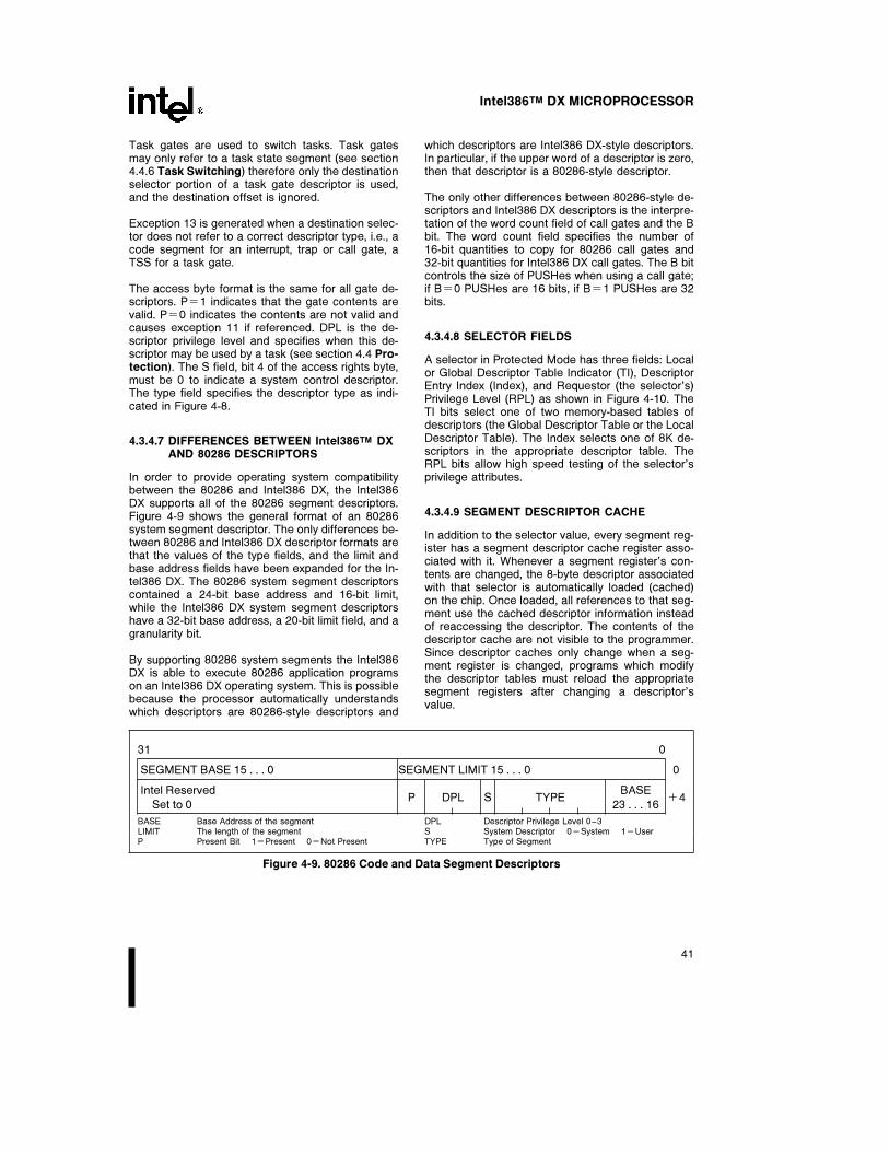
Intel386TM DX MICROPROCESSOR
Task gates are used to switch tasks. Task gatesmay only refer to a task state segment (see section4.4.6 Task Switching) therefore only the destinationselector portion of a task gate descriptor is used,and the destination offset is ignored.
Exception 13 is generated when a destination selec-tor does not refer to a correct descriptor type, i.e., acode segment for an interrupt, trap or call gate, aTSS for a task gate.
The access byte format is the same for all gate de-scriptors. Pe1 indicates that the gate contents arevalid. Pe0 indicates the contents are not valid andcauses exception 11 if referenced. DPL is the de-scriptor privilege level and specifies when this de-scriptor may be used by a task (see section 4.4 Pro-tection). The S field, bit 4 of the access rights byte,must be 0 to indicate a system control descriptor.The type field specifies the descriptor type as indi-cated in Figure 4-8.
4.3.4.7 DIFFERENCES BETWEEN Intel386TM DXAND 80286 DESCRIPTORS
In order to provide operating system compatibilitybetween the 80286 and Intel386 DX, the Intel386DX supports all of the 80286 segment descriptors.Figure 4-9 shows the general format of an 80286system segment descriptor. The only differences be-tween 80286 and Intel386 DX descriptor formats arethat the values of the type fields, and the limit andbase address fields have been expanded for the In-tel386 DX. The 80286 system segment descriptorscontained a 24-bit base address and 16-bit limit,while the Intel386 DX system segment descriptorshave a 32-bit base address, a 20-bit limit field, and agranularity bit.
By supporting 80286 system segments the Intel386DX is able to execute 80286 application programson an Intel386 DX operating system. This is possiblebecause the processor automatically understandswhich descriptors are 80286-style descriptors and
which descriptors are Intel386 DX-style descriptors.In particular, if the upper word of a descriptor is zero,then that descriptor is a 80286-style descriptor.
The only other differences between 80286-style de-scriptors and Intel386 DX descriptors is the interpre-tation of the word count field of call gates and the Bbit. The word count field specifies the number of16-bit quantities to copy for 80286 call gates and32-bit quantities for Intel386 DX call gates. The B bitcontrols the size of PUSHes when using a call gate;if Be0 PUSHes are 16 bits, if Be1 PUSHes are 32bits.
4.3.4.8 SELECTOR FIELDS
A selector in Protected Mode has three fields: Localor Global Descriptor Table Indicator (TI), DescriptorEntry Index (Index), and Requestor (the selector’s)Privilege Level (RPL) as shown in Figure 4-10. TheTI bits select one of two memory-based tables ofdescriptors (the Global Descriptor Table or the LocalDescriptor Table). The Index selects one of 8K de-scriptors in the appropriate descriptor table. TheRPL bits allow high speed testing of the selector’sprivilege attributes.
4.3.4.9 SEGMENT DESCRIPTOR CACHE
In addition to the selector value, every segment reg-ister has a segment descriptor cache register asso-ciated with it. Whenever a segment register’s con-tents are changed, the 8-byte descriptor associatedwith that selector is automatically loaded (cached)on the chip. Once loaded, all references to that seg-ment use the cached descriptor information insteadof reaccessing the descriptor. The contents of thedescriptor cache are not visible to the programmer.Since descriptor caches only change when a seg-ment register is changed, programs which modifythe descriptor tables must reload the appropriatesegment registers after changing a descriptor’svalue.
31 0
SEGMENT BASE 15 . . . 0 SEGMENT LIMIT 15 . . . 0 0
Intel ReservedP DPL S TYPE
BASEa4
Set to 0 23 . . . 16
BASE Base Address of the segmentLIMIT The length of the segmentP Present Bit 1ePresent 0eNot Present
DPL Descriptor Privilege Level 0–3S System Descriptor 0eSystem 1eUserTYPE Type of Segment
Figure 4-9. 80286 Code and Data Segment Descriptors
41

Intel386TM DX MICROPROCESSOR
231630–59
Figure 4-10. Example Descriptor Selection
42
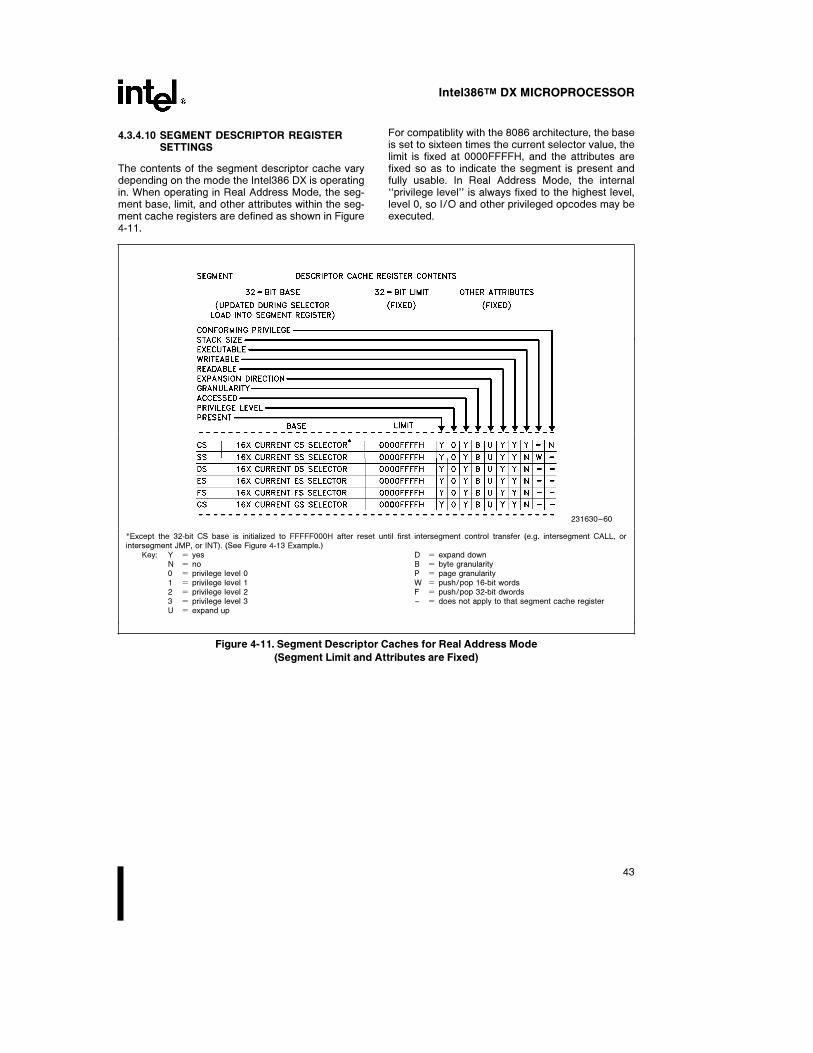
Intel386TM DX MICROPROCESSOR
4.3.4.10 SEGMENT DESCRIPTOR REGISTERSETTINGS
The contents of the segment descriptor cache varydepending on the mode the Intel386 DX is operatingin. When operating in Real Address Mode, the seg-ment base, limit, and other attributes within the seg-ment cache registers are defined as shown in Figure4-11.
For compatiblity with the 8086 architecture, the baseis set to sixteen times the current selector value, thelimit is fixed at 0000FFFFH, and the attributes arefixed so as to indicate the segment is present andfully usable. In Real Address Mode, the internal‘‘privilege level’’ is always fixed to the highest level,level 0, so I/O and other privileged opcodes may beexecuted.
231630–60
*Except the 32-bit CS base is initialized to FFFFF000H after reset until first intersegment control transfer (e.g. intersegment CALL, orintersegment JMP, or INT). (See Figure 4-13 Example.)
Key: Y e yesN e no0 e privilege level 01 e privilege level 12 e privilege level 23 e privilege level 3U e expand up
D e expand downB e byte granularityP e page granularityW e push/pop 16-bit wordsF e push/pop 32-bit dwords– e does not apply to that segment cache register
Figure 4-11. Segment Descriptor Caches for Real Address Mode
(Segment Limit and Attributes are Fixed)
43

Intel386TM DX MICROPROCESSOR
When operating in Protected Mode, the segmentbase, limit, and other attributes within the segmentcache registers are defined as shown in Figure 4-12.In Protected Mode, each of these fields are defined
according to the contents of the segment descriptorindexed by the selector value loaded into the seg-ment register.
231630–61
Key: Y e fixed yesN e fixed nod e per segment descriptorp e per segment descriptor; descriptor must indicate ‘‘present’’ to avoid exception 11
(exception 12 in case of SS)r e per segment descriptor, but descriptor must indicate ‘‘readable’’ to avoid exception 13
(special case for SS)w e per segment descriptor, but descriptor must indicate ‘‘writable’’ to avoid exception 13
(special case for SS)– e does not apply to that segment cache register
Figure 4-12. Segment Descriptor Caches for Protected Mode (Loaded per Descriptor)
44

Intel386TM DX MICROPROCESSOR
When operating in a Virtual 8086 Mode within theProtected Mode, the segment base, limit, and otherattributes within the segment cache registers are de-fined as shown in Figure 4-13. For compatibility withthe 8086 architecture, the base is set to sixteentimes the current selector value, the limit is fixed at
0000FFFFH, and the attributes are fixed so as toindicate the segment is present and fully usable. Thevirtual program executes at lowest privilege level,level 3, to allow trapping of all IOPL-sensitive in-structions and level-0-only instructions.
231630–62
Key: Y e yesN e no0 e privilege level 01 e privilege level 12 e privilege level 23 e privilege level 3U e expand up
D e expand downB e byte granularityP e page granularityW e push/pop 16-bit wordsF e push/pop 32-bit dwords– e does not apply to that segment cache register
Figure 4-13. Segment Descriptor Caches for Virtual 8086 Mode within Protected Mode
(Segment Limit and Attributes are Fixed)
45

Intel386TM DX MICROPROCESSOR
4.4 PROTECTION
4.4.1 Protection Concepts
231630–63
Figure 4-14. Four-Level Hierachical Protection
The Intel386 DX has four levels of protection whichare optimized to support the needs of a multi-taskingoperating system to isolate and protect user pro-grams from each other and the operating system.The privilege levels control the use of privileged in-structions, I/O instructions, and access to segmentsand segment descriptors. Unlike traditional micro-processor-based systems where this protection isachieved only through the use of complex externalhardware and software the Intel386 DX provides theprotection as part of its integrated Memory Manage-ment Unit. The Intel386 DX offers an additional typeof protection on a page basis, when paging is en-abled (See section 4.5.3 Page Level Protection).
The four-level hierarchical privilege system is illus-trated in Figure 4-14. It is an extension of the user/supervisor privilege mode commonly used by mini-computers and, in fact, the user/supervisor mode isfully supported by the Intel386 DX paging mecha-nism. The privilege levels (PL) are numbered 0through 3. Level 0 is the most privileged or trustedlevel.
4.4.2 Rules of Privilege
The Intel386 DX controls access to both data andprocedures between levels of a task, according tothe following rules.
# Data stored in a segment with privilege level p canbe accessed only by code executing at a privilegelevel at least as privileged as p.
# A code segment/procedure with privilege level pcan only be called by a task executing at the sameor a lesser privilege level than p.
4.4.3 Privilege Levels
4.4.3.1 TASK PRIVILEGE
At any point in time, a task on the Intel386 DX al-ways executes at one of the four privilege levels.The Current Privilege Level (CPL) specifies thetask’s privilege level. A task’s CPL may only bechanged by control transfers through gate descrip-tors to a code segment with a different privilege lev-el. (See section 4.4.4 Privilege Level Transfers)Thus, an application program running at PL e 3 maycall an operating system routine at PL e 1 (via agate) which would cause the task’s CPL to be set to1 until the operating system routine was finished.
4.4.3.2 SELECTOR PRIVILEGE (RPL)
The privilege level of a selector is specified by theRPL field. The RPL is the two least significant bits ofthe selector. The selector’s RPL is only used to es-tablish a less trusted privilege level than the currentprivilege level for the use of a segment. This level iscalled the task’s effective privilege level (EPL). TheEPL is defined as being the least privileged (i.e. nu-merically larger) level of a task’s CPL and a selec-tor’s RPL. Thus, if selector’s RPL e 0 then the CPLalways specifies the privilege level for making an ac-cess using the selector. On the other hand if RPL e
3 then a selector can only access segments at level3 regardless of the task’s CPL. The RPL is mostcommonly used to verify that pointers passed to anoperating system procedure do not access data thatis of higher privilege than the procedure that origi-nated the pointer. Since the originator of a selectorcan specify any RPL value, the Adjust RPL (ARPL)instruction is provided to force the RPL bits to theoriginator’s CPL.
4.4.3.3 I/O PRIVILEGE AND I/O PERMISSIONBITMAP
The I/O privilege level (IOPL, a 2-bit field in theEFLAG register) defines the least privileged level atwhich I/O instructions can be unconditionally per-formed. I/O instructions can be unconditionally per-formed when CPL s IOPL. (The I/O instructions areIN, OUT, INS, OUTS, REP INS, and REP OUTS.)When CPL l IOPL, and the current task is associat-ed with a 286 TSS, attempted I/O instructions causean exception 13 fault. When CPL l IOPL, and thecurrent task is associated with an Intel386 DX TSS,the I/O Permission Bitmap (part of an Intel386 DXTSS) is consulted on whether I/O to the port is al-lowed, or an exception 13 fault is to be generated
46
Intel386TM DX MICROPROCESSOR
instead. For diagrams of the I/O Permission Bitmap,refer to Figures 4-15a and 4-15b. For further infor-mation on how the I/O Permission Bitmap is used inProtected Mode or in Virtual 8086 Mode, refer tosection 4.6.4 Protection and I/O Permission Bitmap.
The I/O privilege level (IOPL) also affects whetherseveral other instructions can be executed or causean exception 13 fault instead. These instructions arecalled ‘‘IOPL-sensitive’’ instructions and they areCLI and STI. (Note that the LOCK prefix is not IOPL-sensitive on the Intel386 DX.)
The IOPL also affects whether the IF (interrupts en-able flag) bit can be changed by loading a value intothe EFLAGS register. When CPL s IOPL, then theIF bit can be changed by loading a new value intothe EFLAGS register. When CPL l IOPL, the IF bitcannot be changed by a new value POP’ed into (orotherwise loaded into) the EFLAGS register; the IFbit merely remains unchanged and no exception isgenerated.
Table 4-2. Pointer Test Instructions
Instruction Operands Function
ARPL Selector, Adjust Requested Privi-
Register lege Level: adjusts the
RPL of the selector to the
numeric maximum of
current selector RPL value
and the RPL value in the
register. Set zero flag if
selector RPL was
changed.
VERR Selector VERify for Read: sets the
zero flag if the segment
referred to by the selector
can be read.
VERW Selector VERify for Write: sets the
zero flag if the segment
referred to by the selector
can be written.
LSL Register, Load Segment Limit: reads
Selector the segment limit into the
register if privilege rules
and descriptor type allow.
Set zero flag if successful.
LAR Register, Load Access Rights: reads
Selector the descriptor access
rights byte into the register
if privilege rules allow. Set
zero flag if successful.
4.4.3.4 PRIVILEGE VALIDATION
The Intel386 DX provides several instructions tospeed pointer testing and help maintain system in-tegrity by verifying that the selector value refers toan appropriate segment. Table 4-2 summarizes theselector validation procedures available for the In-tel386 DX.
This pointer verification prevents the common prob-lem of an application at PL e 3 calling a operatingsystems routine at PL e 0 and passing the operat-ing system routine a ‘‘bad’’ pointer which corrupts adata structure belonging to the operating system. Ifthe operating system routine uses the ARPL instruc-tion to ensure that the RPL of the selector has nogreater privilege than that of the caller, then thisproblem can be avoided.
4.4.3.5 DESCRIPTOR ACCESS
There are basically two types of segment accesses:those involving code segments such as controltransfers, and those involving data accesses. Deter-mining the ability of a task to access a segment in-volves the type of segment to be accessed, the in-struction used, the type of descriptor used and CPL,RPL, and DPL as described above.
Any time an instruction loads data segment registers(DS, ES, FS, GS) the Intel386 DX makes protectionvalidation checks. Selectors loaded in the DS, ES,FS, GS registers must refer only to data segments orreadable code segments. The data access rules arespecified in section 4.2.2 Rules of Privilege. Theonly exception to those rules is readable conformingcode segments which can be accessed at any privi-lege level.
Finally the privilege validation checks are performed.The CPL is compared to the EPL and if the EPL ismore privileged than the CPL an exception 13 (gen-eral protection fault) is generated.
The rules regarding the stack segment are slightlydifferent than those involving data segments. In-structions that load selectors into SS must refer todata segment descriptors for writeable data seg-ments. The DPL and RPL must equal the CPL. Allother descriptor types or a privilege level violationwill cause exception 13. A stack not present faultcauses exception 12. Note that an exception 11 isused for a not-present code or data segment.
4.4.4 Privilege Level Transfers
Inter-segment control transfers occur when a selec-tor is loaded in the CS register. For a typical systemmost of these transfers are simply the result of a call
47
Intel386TM DX MICROPROCESSOR
Table 4-3. Descriptor Types Used for Control Transfer
Control Transfer Types Operation TypesDescriptor Descriptor
Referenced Table
Intersegment within the same privilege level JMP, CALL, RET, IRET* Code Segment GDT/LDT
Intersegment to the same or higher privilege level CALL Call Gate GDT/LDT
Interrupt within task may change CPLInterrupt Instruction, Trap or IDT
Exception, External Interrupt
Interrupt Gate
Intersegment to a lower privilege level RET, IRET* Code Segment GDT/LDT
(changes task CPL)
CALL, JMP Task State GDT
Segment
Task SwitchCALL, JMP Task Gate GDT/LDT
IRET** Task Gate IDT
Interrupt Instruction,
Exception, External
Interrupt
*NT (Nested Task bit of flag register) e 0**NT (Nested Task bit of flag register) e 1
or a jump to another routine. There are five types ofcontrol transfers which are summarized in Table 4-3.Many of these transfers result in a privilege leveltransfer. Changing privilege levels is done only viacontrol transfers, by using gates, task switches, andinterrupt or trap gates.
Control transfers can only occur if the operationwhich loaded the selector references the correct de-scriptor type. Any violation of these descriptor usagerules will cause an exception 13 (e.g. JMP through acall gate, or IRET from a normal subroutine call).
In order to provide further system security, all controltransfers are also subject to the privilege rules.
The privilege rules require that:
Ð Privilege level transitions can only occur viagates.
Ð JMPs can be made to a non-conforming codesegment with the same privilege or to a conform-ing code segment with greater or equal privilege.
Ð CALLs can be made to a non-conforming codesegment with the same privilege or via a gate to amore privileged level.
Ð Interrupts handled within the task obey the sameprivilege rules as CALLs.
Ð Conforming Code segments are accessible byprivilege levels which are the same or less privi-leged than the conforming-code segment’s DPL.
Ð Both the requested privilege level (RPL) in theselector pointing to the gate and the task’s CPL
must be of equal or greater privilege than thegate’s DPL.
Ð The code segment selected in the gate must bethe same or more privileged than the task’s CPL.
Ð Return instructions that do not switch tasks canonly return control to a code segment with sameor less privilege.
Ð Task switches can be performed by a CALL,JMP, or INT which references either a task gateor task state segment who’s DPL is less privi-leged or the same privilege as the old task’s CPL.
Any control transfer that changes CPL within a taskcauses a change of stacks as a result of the privi-lege level change. The initial values of SS:ESP forprivilege levels 0, 1, and 2 are retained in the taskstate segment (see section 4.4.6 Task Switching).During a JMP or CALL control transfer, the newstack pointer is loaded into the SS and ESP regis-ters and the previous stack pointer is pushed ontothe new stack.
When RETurning to the original privilege level, useof the lower-privileged stack is restored as part ofthe RET or IRET instruction operation. For subrou-tine calls that pass parameters on the stack andcross privilege levels, a fixed number of words (asspecified in the gate’s word count field) are copiedfrom the previous stack to the current stack. Theinter-segment RET instruction with a stack adjust-ment value will correctly restore the previous stackpointer upon return.
48
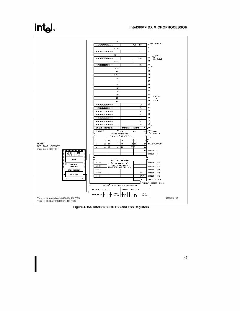
Intel386TM DX MICROPROCESSOR
NOTE:BITÐMAPÐOFFSETmust be s DFFFH
231630–64Type e 9: Available Intel386TM DX TSS,Type e B: Busy Intel386TM DX TSS
Figure 4-15a. Intel386TM DX TSS and TSS Registers
49
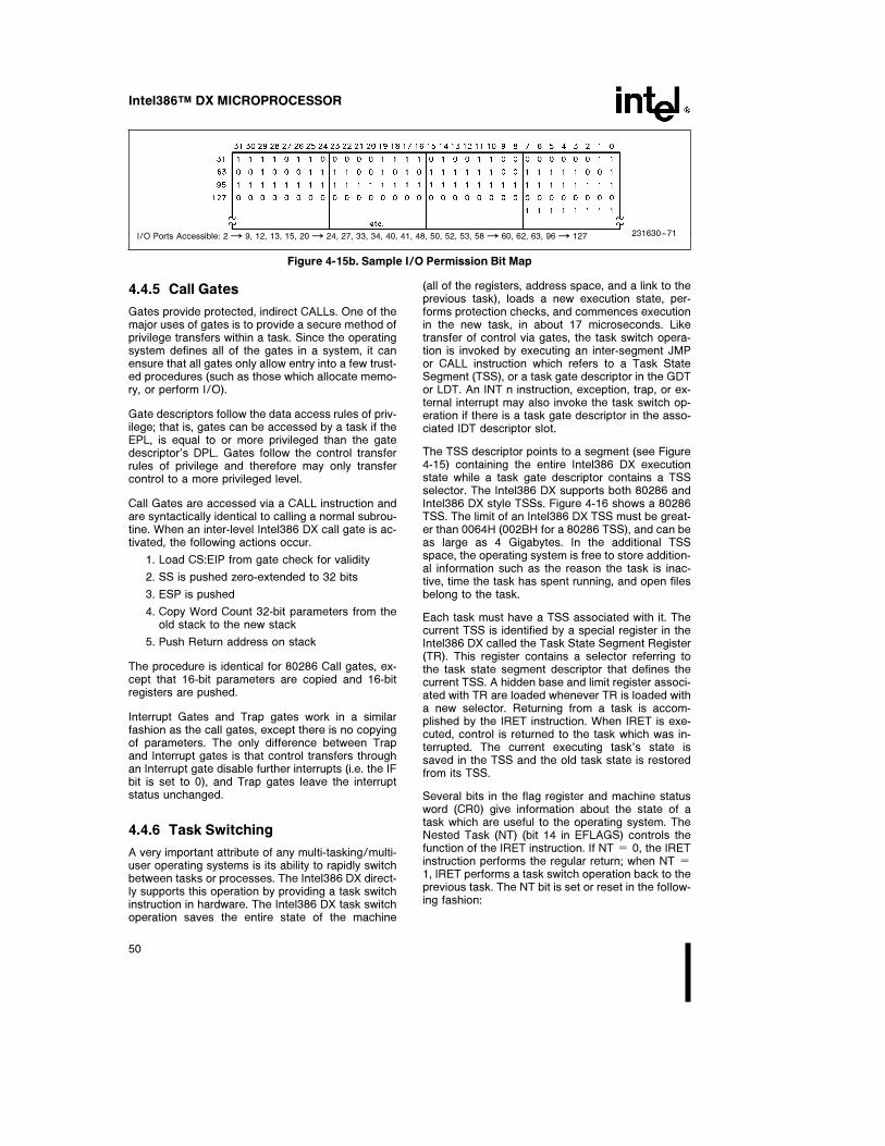
Intel386TM DX MICROPROCESSOR
231630–71I/O Ports Accessible: 2x9, 12, 13, 15, 20x24, 27, 33, 34, 40, 41, 48, 50, 52, 53, 58x60, 62, 63, 96x127
Figure 4-15b. Sample I/O Permission Bit Map
4.4.5 Call Gates
Gates provide protected, indirect CALLs. One of themajor uses of gates is to provide a secure method ofprivilege transfers within a task. Since the operatingsystem defines all of the gates in a system, it canensure that all gates only allow entry into a few trust-ed procedures (such as those which allocate memo-ry, or perform I/O).
Gate descriptors follow the data access rules of priv-ilege; that is, gates can be accessed by a task if theEPL, is equal to or more privileged than the gatedescriptor’s DPL. Gates follow the control transferrules of privilege and therefore may only transfercontrol to a more privileged level.
Call Gates are accessed via a CALL instruction andare syntactically identical to calling a normal subrou-tine. When an inter-level Intel386 DX call gate is ac-tivated, the following actions occur.
1. Load CS:EIP from gate check for validity
2. SS is pushed zero-extended to 32 bits
3. ESP is pushed
4. Copy Word Count 32-bit parameters from theold stack to the new stack
5. Push Return address on stack
The procedure is identical for 80286 Call gates, ex-cept that 16-bit parameters are copied and 16-bitregisters are pushed.
Interrupt Gates and Trap gates work in a similarfashion as the call gates, except there is no copyingof parameters. The only difference between Trapand Interrupt gates is that control transfers throughan Interrupt gate disable further interrupts (i.e. the IFbit is set to 0), and Trap gates leave the interruptstatus unchanged.
4.4.6 Task Switching
A very important attribute of any multi-tasking/multi-user operating systems is its ability to rapidly switchbetween tasks or processes. The Intel386 DX direct-ly supports this operation by providing a task switchinstruction in hardware. The Intel386 DX task switchoperation saves the entire state of the machine
(all of the registers, address space, and a link to theprevious task), loads a new execution state, per-forms protection checks, and commences executionin the new task, in about 17 microseconds. Liketransfer of control via gates, the task switch opera-tion is invoked by executing an inter-segment JMPor CALL instruction which refers to a Task StateSegment (TSS), or a task gate descriptor in the GDTor LDT. An INT n instruction, exception, trap, or ex-ternal interrupt may also invoke the task switch op-eration if there is a task gate descriptor in the asso-ciated IDT descriptor slot.
The TSS descriptor points to a segment (see Figure4-15) containing the entire Intel386 DX executionstate while a task gate descriptor contains a TSSselector. The Intel386 DX supports both 80286 andIntel386 DX style TSSs. Figure 4-16 shows a 80286TSS. The limit of an Intel386 DX TSS must be great-er than 0064H (002BH for a 80286 TSS), and can beas large as 4 Gigabytes. In the additional TSSspace, the operating system is free to store addition-al information such as the reason the task is inac-tive, time the task has spent running, and open filesbelong to the task.
Each task must have a TSS associated with it. Thecurrent TSS is identified by a special register in theIntel386 DX called the Task State Segment Register(TR). This register contains a selector referring tothe task state segment descriptor that defines thecurrent TSS. A hidden base and limit register associ-ated with TR are loaded whenever TR is loaded witha new selector. Returning from a task is accom-plished by the IRET instruction. When IRET is exe-cuted, control is returned to the task which was in-terrupted. The current executing task’s state issaved in the TSS and the old task state is restoredfrom its TSS.
Several bits in the flag register and machine statusword (CR0) give information about the state of atask which are useful to the operating system. TheNested Task (NT) (bit 14 in EFLAGS) controls thefunction of the IRET instruction. If NT e 0, the IRETinstruction performs the regular return; when NT e
1, IRET performs a task switch operation back to theprevious task. The NT bit is set or reset in the follow-ing fashion:
50

Intel386TM DX MICROPROCESSOR
231630–65
Figure 4-16. 80286 TSS
When a CALL or INT instruction initiates a taskswitch, the new TSS will be marked busy and theback link field of the new TSS set to the old TSSselector. The NT bit of the new task is set by CALLor INT initiated task switches. An interrupt that doesnot cause a task switch will clear NT. (The NT bit willbe restored after execution of the interrupt handler)NT may also be set or cleared by POPF or IRETinstructions.
The Intel386 DX task state segment is marked busyby changing the descriptor type field from TYPE 9Hto TYPE BH. An 80286 TSS is marked busy bychanging the descriptor type field from TYPE 1 toTYPE 3. Use of a selector that references a busytask state segment causes an exception 13.
The Virtual Mode (VM) bit 17 is used to indicate if atask, is a virtual 8086 task. If VM e 1, then the taskswill use the Real Mode addressing mechanism. Thevirtual 8086 environment is only entered and exitedvia a task switch (see section 4.6 Virtual Mode).
The coprocessor’s state is not automatically savedwhen a task switch occurs, because the incomingtask may not use the coprocessor. The TaskSwitched (TS) Bit (bit 3 in the CR0) helps deal withthe coprocessor’s state in a multi-tasking environ-
ment. Whenever the Intel386 DX switches tasks, itsets the TS bit. The Intel386 DX detects the first useof a processor extension instruction after a taskswitch and causes the processor extension notavailable exception 7. The exception handler for ex-ception 7 may then decide whether to save the stateof the coprocessor. A processor extension not pres-ent exception (7) will occur when attempting to exe-cute an ESC or WAIT instruction if the TaskSwitched and Monitor coprocessor extension bitsare both set (i.e. TS e 1 and MP e 1).
The T bit in the Intel386 DX TSS indicates that theprocessor should generate a debug exception whenswitching to a task. If T e 1 then upon entry to anew task a debug exception 1 will be generated.
4.4.7 Initialization and Transition toProtected Mode
Since the Intel386 DX begins executing in RealMode immediately after RESET it is necessary toinitialize the system tables and registers with the ap-propriate values.
The GDT and IDT registers must refer to a valid GDTand IDT. The IDT should be at least 256 bytes long,and GDT must contain descriptors for the initialcode, and data segments. Figure 4-17 shows thetables and Figure 4-18 the descriptors needed for asimple Protected Mode Intel386 DX system. It has asingle code and single data/stack segment eachfour gigabytes long and a single privilege level PL e
0.
The actual method of enabling Protected Mode is toload CR0 with the PE bit set, via the MOV CR0, R/Minstruction. This puts the Intel386 DX in ProtectedMode.
After enabling Protected Mode, the next instructionshould execute an intersegment JMP to load the CSregister and flush the instruction decode queue. Thefinal step is to load all of the data segment registerswith the initial selector values.
An alternate approach to entering Protected Modewhich is especially appropriate for multi-tasking op-erating systems, is to use the built in task-switch toload all of the registers. In this case the GDT wouldcontain two TSS descriptors in addition to the codeand data descriptors needed for the first task. Thefirst JMP instruction in Protected Mode would jumpto the TSS causing a task switch and loading all ofthe registers with the values stored in the TSS. TheTask State Segment Register should be initialized topoint to a valid TSS descriptor since a task switchsaves the state of the current task in a task statesegment.
51

Intel386TM DX MICROPROCESSOR
231630–66
Figure 4-17. Simple Protected System
DATA SEGMENT BASE 15 . . . 0 SEGMENT LIMIT 15 . . . 0
DESCRIPTOR 0118 (H) FFFF (H)
BASE 31 . . . 24 G DLIMIT
BASE 23 . . . 16
00 (H) 1 10 0 19.16 1 0 0 1 0 0 1 0
00 (H)F (H)
CODE SEGMENT BASE 15 . . . 0 SEGMENT LIMIT 15 . . . 0
DESCRIPTOR 0118 (H) FFFF (H)
BASE 31 . . . 24 G DLIMIT
BASE 23 . . . 16
00 (H) 1 10 0 19.16 1 0 0 1 1 0 1 0
00 (H)F (H)
NULL DESCRIPTOR
31 24 16 15 8 0
Figure 4-18. GDT Descriptors for Simple System
4.4.8 Tools for Building ProtectedSystems
In order to simplify the design of a protected multi-tasking system, Intel provides a tool which allowsthe system designer an easy method of constructingthe data structures needed for a Protected ModeIntel386 DX system. This tool is the builder BLD-386.BLD-386 lets the operating system writer specify allof the segment descriptors discussed in the previoussections (LDTs, IDTs, GDTs, Gates, and TSSs) in ahigh-level language.
4.5 PAGING
4.5.1 Paging Concepts
Paging is another type of memory management use-ful for virtual memory multitasking operating sys-tems. Unlike segmentation which modularizes pro-grams and data into variable length segments,paging divides programs into multiple uniform sizepages. Pages bear no direct relation to the logical
52

Intel386TM DX MICROPROCESSOR
structure of a program. While segment selectors canbe considered the logical ‘‘name’’ of a programmodule or data structure, a page most likely corre-sponds to only a portion of a module or data struc-ture.
By taking advantage of the locality of reference dis-played by most programs, only a small number ofpages from each active task need be in memory atany one moment.
4.5.2 Paging Organization
4.5.2.1 PAGE MECHANISM
The Intel386 DX uses two levels of tables to trans-late the linear address (from the segmentation unit)into a physical address. There are three compo-nents to the paging mechanism of the Intel386 DX:the page directory, the page tables, and the pageitself (page frame). All memory-resident elements ofthe Intel386 DX paging mechanism are the samesize, namely, 4K bytes. A uniform size for all of theelements simplifies memory allocation and realloca-tion schemes, since there is no problem with memo-ry fragmentation. Figure 4-19 shows how the pagingmechanism works.
4.5.2.2 PAGE DESCRIPTOR BASE REGISTER
CR2 is the Page Fault Linear Address register. Itholds the 32-bit linear address which caused the lastpage fault detected.
CR3 is the Page Directory Physical Base AddressRegister. It contains the physical starting address ofthe Page Directory. The lower 12 bits of CR3 arealways zero to ensure that the Page Directory is al-ways page aligned. Loading it via a MOV CR3, reginstruction causes the Page Table Entry cache to beflushed, as will a task switch through a TSS whichchanges the value of CR0. (See 4.5.4 TranslationLookaside Buffer).
4.5.2.3 PAGE DIRECTORY
The Page Directory is 4K bytes long and allows up to1024 Page Directory Entries. Each Page DirectoryEntry contains the address of the next level of ta-bles, the Page Tables and information about thepage table. The contents of a Page Directory Entryare shown in Figure 4-20. The upper 10 bits of thelinear address (A22–A31) are used as an index toselect the correct Page Directory Entry.
231630–67
Figure 4-19. Paging Mechanism
31 12 11 10 9 8 7 6 5 4 3 2 1 0
OS U R
PAGE TABLE ADDRESS 31..12 RESERVED 0 0 D A 0 0 Ð Ð P
S W
Figure 4-20. Page Directory Entry (Points to Page Table)
53
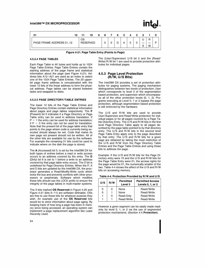
Intel386TM DX MICROPROCESSOR
31 12 11 10 9 8 7 6 5 4 3 2 1 0
OS U RPAGE FRAME ADDRESS 31..12 RESERVED 0 0 D A 0 0 Ð Ð P
S W
Figure 4-21. Page Table Entry (Points to Page)
4.5.2.4 PAGE TABLES
Each Page Table is 4K bytes and holds up to 1024Page Table Entries. Page Table Entries contain thestarting address of the page frame and statisticalinformation about the page (see Figure 4-21). Ad-dress bits A12–A21 are used as an index to selectone of the 1024 Page Table Entries. The 20 upper-bit page frame address is concatenated with thelower 12 bits of the linear address to form the physi-cal address. Page tables can be shared betweentasks and swapped to disks.
4.5.2.5 PAGE DIRECTORY/TABLE ENTRIES
The lower 12 bits of the Page Table Entries andPage Directory Entries contain statistical informationabout pages and page tables respectively. The P(Present) bit 0 indicates if a Page Directory or PageTable entry can be used in address translation. IfP e 1 the entry can be used for address translation;if P e 0 the entry can not be used for translation.Note that the present bit of the page table entry thatpoints to the page where code is currently being ex-ecuted should always be set. Code that marks itsown page not present should not be written. All ofthe other bits are available for use by the software.For example the remaining 31 bits could be used toindicate where on the disk the page is stored.
The A (Accessed) bit 5, is set by the Intel386 DX forboth types of entries before a read or write accessoccurs to an address covered by the entry. The D(Dirty) bit 6 is set to 1 before a write to an addresscovered by that page table entry occurs. The D bit isundefined for Page Directory Entries. When the P, Aand D bits are updated by the Intel386 DX, the proc-essor generates a Read-Modify-Write cycle whichlocks the bus and prevents conflicts with other proc-essors or perpherials. Software which modifiesthese bits should use the LOCK prefix to ensure theintegrity of the page tables in multi-master systems.
The 3 bits marked OS Reserved in Figure 4-20 andFigure 4-21 (bits 9–11) are software definable. OSsare free to use these bits for whatever purpose theywish. An example use of the OS Reserved bitswould be to store information about page aging. Bykeeping track of how long a page has been in mem-ory since being accessed, an operating system canimplement a page replacement algorithm like LeastRecently Used.
The (User/Supervisor) U/S bit 2 and the (Read/Write) R/W bit 1 are used to provide protection attri-butes for individual pages.
4.5.3 Page Level Protection(R/W, U/S Bits)
The Intel386 DX provides a set of protection attri-butes for paging systems. The paging mechanismdistinguishes between two levels of protection: Userwhich corresponds to level 3 of the segmentationbased protection, and supervisor which encompass-es all of the other protection levels (0, 1, 2). Pro-grams executing at Level 0, 1 or 2 bypass the pageprotection, although segmentation based protectionis still enforced by the hardware.
The U/S and R/W bits are used to provideUser/Supervisor and Read/Write protection for indi-vidual pages or for all pages covered by a Page Ta-ble Directory Entry. The U/S and R/W bits in the firstlevel Page Directory Table apply to all pages de-scribed by the page table pointed to by that directoryentry. The U/S and R/W bits in the second levelPage Table Entry apply only to the page describedby that entry. The U/S and R/W bits for a givenpage are obtained by taking the most restrictive ofthe U/S and R/W from the Page Directory TableEntries and the Page Table Entries and using thesebits to address the page.
Example: If the U/S and R/W bits for the Page Di-rectory entry were 10 and the U/S and R/W bits forthe Page Table Entry were 01, the access rights forthe page would be 01, the numerically smaller of thetwo. Table 4-4 shows the affect of the U/S and R/Wbits on accessing memory.
Table 4-4. Protection Provided by R/W and U/S
U/S R/WPermitted Permitted Access
Level 3 Levels 0, 1, or 2
0 0 None Read/Write
0 1 None Read/Write
1 0 Read-Only Read/Write
1 1 Read/Write Read/Write
However a given segment can be easily made read-only for level 0, 1, or 2 via the use of segmentedprotection mechanisms. (Section 4.4 Protection).
54

Intel386TM DX MICROPROCESSOR
4.5.4 Translation Lookaside Buffer
The Intel386 DX paging hardware is designed tosupport demand paged virtual memory systems.However, performance would degrade substantiallyif the processor was required to access two levels oftables for every memory reference. To solve thisproblem, the Intel386 DX keeps a cache of the mostrecently accessed pages, this cache is called theTranslation Lookaside Buffer (TLB). The TLB is afour-way set associative 32-entry page table cache.It automatically keeps the most commonly usedPage Table Entries in the processor. The 32-entryTLB coupled with a 4K page size, results in cover-age of 128K bytes of memory addresses. For manycommon multi-tasking systems, the TLB will have ahit rate of about 98%. This means that the proces-sor will only have to access the two-level page struc-ture on 2% of all memory references. Figure 4-22illustrates how the TLB complements the Intel386DX’s paging mechanism.
4.5.5 Paging Operation
231630–68
Figure 4-22. Translation Lookaside Buffer
The paging hardware operates in the following fash-ion. The paging unit hardware receives a 32-bit lin-ear address from the segmentation unit. The upper20 linear address bits are compared with all 32 en-tries in the TLB to determine if there is a match. Ifthere is a match (i.e. a TLB hit), then the 32-bit phys-ical address is calculated and will be placed on theaddress bus.
However, if the page table entry is not in the TLB,the Intel386 DX will read the appropriate Page Direc-tory Entry. If P e 1 on the Page Directory Entry indi-cating that the page table is in memory, then theIntel386 DX will read the appropriate Page Table En-
try and set the Access bit. If P e 1 on the PageTable Entry indicating that the page is in memory,the Intel386 DX will update the Access and Dirty bitsas needed and fetch the operand. The upper 20 bitsof the linear address, read from the page table, willbe stored in the TLB for future accesses. However, ifP e 0 for either the Page Directory Entry or thePage Table Entry, then the processor will generate apage fault, an Exception 14.
The processor will also generate an exception 14,page fault, if the memory reference violated thepage protection attributes (i.e. U/S or R/W) (e.g. try-ing to write to a read-only page). CR2 will hold thelinear address which caused the page fault. If a sec-ond page fault occurs, while the processor is at-tempting to enter the service routine for the first,then the processor will invoke the page fault (excep-tion 14) handler a second time, rather than the dou-ble fault (exception 8) handler. Since Exception 14 isclassified as a fault, CS: EIP will point to the instruc-tion causing the page fault. The 16-bit error codepushed as part of the page fault handler will containstatus bits which indicate the cause of the pagefault.
The 16-bit error code is used by the operating sys-tem to determine how to handle the page fault Fig-ure 4-23A shows the format of the page-fault errorcode and the interpretation of the bits.
NOTE:Even though the bits in the error code (U/S, W/R,and P) have similar names as the bits in the PageDirectory/Table Entries, the interpretation of the er-ror code bits is different. Figure 4-23B indicateswhat type of access caused the page fault.
15 3 2 1 0
U
U U U U U U U U U U U U U U W P
S R
Figure 4-23A. Page Fault Error Code Format
U/S: The U/S bit indicates whether the accesscausing the fault occurred when the processor wasexecuting in User Mode (U/S e 1) or in Supervisormode (U/S e 0)
W/R: The W/R bit indicates whether the accesscausing the fault was a Read (W/R e 0) or a Write(W/R e 1)
P: The P bit indicates whether a page fault wascaused by a not-present page (P e 0), or by a pagelevel protection violation (P e 1)
U: UNDEFINED
55
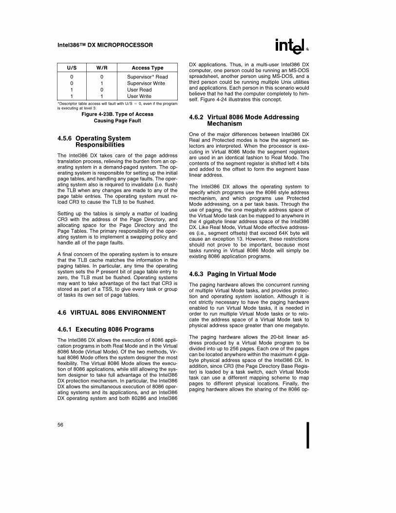
Intel386TM DX MICROPROCESSOR
U/S W/R Access Type
0 0 Supervisor* Read
0 1 Supervisor Write
1 0 User Read
1 1 User Write
*Descriptor table access will fault with U/S e 0, even if the programis executing at level 3.
Figure 4-23B. Type of Access
Causing Page Fault
4.5.6 Operating SystemResponsibilities
The Intel386 DX takes care of the page addresstranslation process, relieving the burden from an op-erating system in a demand-paged system. The op-erating system is responsible for setting up the initialpage tables, and handling any page faults. The oper-ating system also is required to invalidate (i.e. flush)the TLB when any changes are made to any of thepage table entries. The operating system must re-load CR3 to cause the TLB to be flushed.
Setting up the tables is simply a matter of loadingCR3 with the address of the Page Directory, andallocating space for the Page Directory and thePage Tables. The primary responsibility of the oper-ating system is to implement a swapping policy andhandle all of the page faults.
A final concern of the operating system is to ensurethat the TLB cache matches the information in thepaging tables. In particular, any time the operatingsystem sets the P present bit of page table entry tozero, the TLB must be flushed. Operating systemsmay want to take advantage of the fact that CR3 isstored as part of a TSS, to give every task or groupof tasks its own set of page tables.
4.6 VIRTUAL 8086 ENVIRONMENT
4.6.1 Executing 8086 Programs
The Intel386 DX allows the execution of 8086 appli-cation programs in both Real Mode and in the Virtual8086 Mode (Virtual Mode). Of the two methods, Vir-tual 8086 Mode offers the system designer the mostflexibility. The Virtual 8086 Mode allows the execu-tion of 8086 applications, while still allowing the sys-tem designer to take full advantage of the Intel386DX protection mechanism. In particular, the Intel386DX allows the simultaneous execution of 8086 oper-ating systems and its applications, and an Intel386DX operating system and both 80286 and Intel386
DX applications. Thus, in a multi-user Intel386 DXcomputer, one person could be running an MS-DOSspreadsheet, another person using MS-DOS, and athird person could be running multiple Unix utilitiesand applications. Each person in this scenario wouldbelieve that he had the computer completely to him-self. Figure 4-24 illustrates this concept.
4.6.2 Virtual 8086 Mode AddressingMechanism
One of the major differences between Intel386 DXReal and Protected modes is how the segment se-lectors are interpreted. When the processor is exe-cuting in Virtual 8086 Mode the segment registersare used in an identical fashion to Real Mode. Thecontents of the segment register is shifted left 4 bitsand added to the offset to form the segment baselinear address.
The Intel386 DX allows the operating system tospecify which programs use the 8086 style addressmechanism, and which programs use ProtectedMode addressing, on a per task basis. Through theuse of paging, the one megabyte address space ofthe Virtual Mode task can be mapped to anywhere inthe 4 gigabyte linear address space of the Intel386DX. Like Real Mode, Virtual Mode effective address-es (i.e., segment offsets) that exceed 64K byte willcause an exception 13. However, these restrictionsshould not prove to be important, because mosttasks running in Virtual 8086 Mode will simply beexisting 8086 application programs.
4.6.3 Paging In Virtual Mode
The paging hardware allows the concurrent runningof multiple Virtual Mode tasks, and provides protec-tion and operating system isolation. Although it isnot strictly necessary to have the paging hardwareenabled to run Virtual Mode tasks, it is needed inorder to run multiple Virtual Mode tasks or to relo-cate the address space of a Virtual Mode task tophysical address space greater than one megabyte.
The paging hardware allows the 20-bit linear ad-dress produced by a Virtual Mode program to bedivided into up to 256 pages. Each one of the pagescan be located anywhere within the maximum 4 giga-byte physical address space of the Intel386 DX. Inaddition, since CR3 (the Page Directory Base Regis-ter) is loaded by a task switch, each Virtual Modetask can use a different mapping scheme to mappages to different physical locations. Finally, thepaging hardware allows the sharing of the 8086 op-
56

Intel386TM DX MICROPROCESSOR
231630–69
Figure 4-24. Virtual 8086 Environment Memory Management
erating system code between multiple 8086 applica-tions. Figure 4-24 shows how the Intel386 DX paginghardware enables multiple 8086 programs to run un-der a virtual memory demand paged system.
4.6.4 Protection and I/O PermissionBitmap
All Virtual 8086 Mode programs execute at privilegelevel 3, the level of least privilege. As such, Virtual8086 Mode programs are subject to all of the protec-tion checks defined in Protected Mode. (This is dif-ferent from Real Mode which implicitly is executingat privilege level 0, the level of greatest privilege.)Thus, an attempt to execute a privileged instructionwhen in Virtual 8086 Mode will cause an exception13 fault.
The following are privileged instructions, which maybe executed only at Privilege Level 0. Therefore, at-tempting to execute these instructions in Virtual8086 Mode (or anytime CPL l 0) causes an excep-tion 13 fault:
LIDT; MOV DRn,reg; MOV reg,DRn;LGDT; MOV TRn,reg; MOV reg,TRn;
LMSW; MOV CRn,reg; MOV reg,CRn.CLTS;HLT;
Several instructions, particularly those applying tothe multitasking model and protection model, areavailable only in Protected Mode. Therefore, at-tempting to execute the following instructions inReal Mode or in Virtual 8086 Mode generates anexception 6 fault:
LTR; STR;LLDT; SLDT;LAR; VERR;LSL; VERW;ARPL.
The instructions which are IOPL-sensitive in Protect-ed Mode are:
IN; STI;OUT; CLIINS;OUTS;REP INS;REP OUTS;
57

Intel386TM DX MICROPROCESSOR
In Virtual 8086 Mode, a slightly different set of in-structions are made IOPL-sensitive. The following in-structions are IOPL-sensitive in Virtual 8086 Mode:
INT n; STI;PUSHF; CLI;POPF; IRET
The PUSHF, POPF, and IRET instructions are IOPL-sensitive in Virtual 8086 Mode only. This provisionallows the IF flag (interrupt enable flag) to be virtual-ized to the Virtual 8086 Mode program. The INT nsoftware interrupt instruction is also IOPL-sensitivein Virtual 8086 Mode. Note, however, that the INT 3(opcode 0CCH), INTO, and BOUND instructions arenot IOPL-sensitive in Virtual 8086 mode (they aren’tIOPL sensitive in Protected Mode either).
Note that the I/O instructions (IN, OUT, INS, OUTS,REP INS, and REP OUTS) are not IOPL-sensitive inVirtual 8086 mode. Rather, the I/O instructions be-come automatically sensitive to the I/O PermissionBitmap contained in the Intel386 DX Task StateSegment. The I/O Permission Bitmap, automaticallyused by the Intel386 DX in Virtual 8086 Mode, isillustrated by Figures 4.15a and 4-15b.
The I/O Permission Bitmap can be viewed as a 0–64 Kbit bit string, which begins in memory at offsetBitÐMapÐOffset in the current TSS. BitÐMapÐOffset must be s DFFFH so the entire bit map andthe byte FFH which follows the bit map are all atoffsets s FFFFH from the TSS base. The 16-bitpointer BitÐMapÐOffset (15:0) is found in the wordbeginning at offset 66H (102 decimal) from the TSSbase, as shown in Figure 4-15a.
Each bit in the I/O Permission Bitmap correspondsto a single byte-wide I/O port, as illustrated in Figure4-15a. If a bit is 0, I/O to the corresponding byte-wide port can occur without generating an excep-tion. Otherwise the I/O instruction causes an excep-tion 13 fault. Since every byte-wide I/O port must beprotectable, all bits corresponding to a word-wide ordword-wide port must be 0 for the word-wide ordword-wide I/O to be permitted. If all the referencedbits are 0, the I/O will be allowed. If any referencedbits are 1, the attempted I/O will cause an exception13 fault.
Due to the use of a pointer to the base of the I/OPermission Bitmap, the bitmap may be located any-where within the TSS, or may be ignored completelyby pointing the BitÐMapÐOffset (15:0) beyond thelimit of the TSS segment. In the same manner, onlya small portion of the 64K I/O space need have anassociated map bit, by adjusting the TSS limit totruncate the bitmap. This eliminates the commitmentof 8K of memory when a complete bitmap is notrequired, while allowing the fully general case ifdesired.
EXAMPLE OF BITMAP FOR I/O PORTS 0–255:Setting the TSS limit to ÀbitÐMapÐOffset a 31a1**Ó [** see note below] will allow a 32-byte bit-map for the I/O ports Ý0–255, plus a terminatorbyte of all 1’s [** see note below]. This allows theI/O bitmap to control I/O Permission to I/O port 0–255 while causing an exception 13 fault on attempt-ed I/O to any I/O port 80256 through 65,565.
**IMPORTANT IMPLEMENTATION NOTE: Beyondthe last byte of I/O mapping information in the I/OPermission Bitmap must be a byte containing all 1’s.The byte of all 1’s must be within the limit of theIntel386 DX TSS segment (see Figure 4-15a).
4.6.5 Interrupt Handling
In order to fully support the emulation of an 8086machine, interrupts in Virtual 8086 Mode are han-dled in a unique fashion. When running in VirtualMode all interrupts and exceptions involve a privi-lege change back to the host Intel386 DX operatingsystem. The Intel386 DX operating system deter-mines if the interrupt comes from a Protected Modeapplication or from a Virtual Mode program by exam-ining the VM bit in the EFLAGS image stored on thestack.
When a Virtual Mode program is interrupted and ex-ecution passes to the interrupt routine at level 0, theVM bit is cleared. However, the VM bit is still set inthe EFLAG image on the stack.
The Intel386 DX operating system in turn handlesthe exception or interrupt and then returns control tothe 8086 program. The Intel386 DX operating sys-tem may choose to let the 8086 operating systemhandle the interrupt or it may emulate the function ofthe interrupt handler. For example, many 8086 oper-ating system calls are accessed by PUSHing param-eters on the stack, and then executing an INT n in-struction. If the IOPL is set to 0 then all INT n instruc-tions will be intercepted by the Intel386 DX Micro-processor operating system. The Intel386 DX oper-ating system could emulate the 8086 operating sys-tem’s call. Figure 4-25 shows how the Intel386 DXoperating system could intercept an 8086 operatingsystem’s call to ‘‘Open a File’’.
An Intel386 DX operating system can provide a Vir-tual 8086 Environment which is totally transparent tothe application software via intercepting and thenemulating 8086 operating system’s calls, and inter-cepting IN and OUT instructions.
58

Intel386TM DX MICROPROCESSOR
4.6.6 Entering and Leaving Virtual8086 Mode
Virtual 8086 mode is entered by executing an IRETinstruction (at CPLe0), or Task Switch (at any CPL)to an Intel386 DX task whose Intel386 DX TSS has aFLAGS image containing a 1 in the VM bit positionwhile the processor is executing in Protected Mode.That is, one way to enter Virtual 8086 mode is toswitch to a task with an Intel386 DX TSS that has a1 in the VM bit in the EFLAGS image. The other wayis to execute a 32-bit IRET instruction at privilegelevel 0, where the stack has a 1 in the VM bit in theEFLAGS image. POPF does not affect the VM bit,even if the processor is in Protected Mode or level 0,and so cannot be used to enter Virtual 8086 Mode.PUSHF always pushes a 0 in the VM bit, even if theprocessor is in Virtual 8086 Mode, so that a programcannot tell if it is executing in REAL mode, or in Vir-tual 8086 mode.
The VM bit can be set by executing an IRET instruc-tion only at privilege level 0, or by any instruction orInterrupt which causes a task switch in ProtectedMode (with VMe1 in the new FLAGS image), andcan be cleared only by an interrupt or exception inVirtual 8086 Mode. IRET and POPF instructions exe-cuted in REAL mode or Virtual 8086 mode will notchange the value in the VM bit.
The transition out of virtual 8086 mode to Intel386DX protected mode occurs only on receipt of an in-terrupt or exception (such as due to a sensitive in-struction). In Virtual 8086 mode, all interrupts andexceptions vector through the protected mode IDT,and enter an interrupt handler in protected Intel386DX mode. That is, as part of interrupt processing,the VM bit is cleared.
Because the matching IRET must occur from level 0,if an Interrupt or Trap Gate is used to field an inter-rupt or exception out of Virtual 8086 mode, the Gatemust perform an inter-level interrupt only to level 0.Interrupt or Trap Gates through conforming seg-ments, or through segments with DPLl0, will raise aGP fault with the CS selector as the error code.
4.6.6.1 TASK SWITCHES TO/FROM VIRTUAL8086 MODE
Tasks which can execute in virtual 8086 mode mustbe described by a TSS with the new Intel386 DXformat (TYPE 9 or 11 descriptor).
A task switch out of virtual 8086 mode will operateexactly the same as any other task switch out of atask with an Intel386 DX TSS. All of the programmervisible state, including the FLAGS register with theVM bit set to 1, is stored in the TSS. The segment
registers in the TSS will contain 8086 segment basevalues rather than selectors.
A task switch into a task described by an Intel386DX TSS will have an additional check to determine ifthe incoming task should be resumed in virtual 8086mode. Tasks described by 80286 format TSSs can-not be resumed in virtual 8086 mode, so no check isrequired there (the FLAGS image in 80286 formatTSS has only the low order 16 FLAGS bits). Beforeloading the segment register images from an In-tel386 DX TSS, the FLAGS image is loaded, so thatthe segment registers are loaded from the TSS im-age as 8086 segment base values. The task is nowready to resume in virtual 8086 execution mode.
4.6.6.2 TRANSITIONS THROUGH TRAP ANDINTERRUPT GATES, AND IRET
A task switch is one way to enter or exit virtual 8086mode. The other method is to exit through a Trap orInterrupt gate, as part of handling an interrupt, andto enter as part of executing an IRET instruction.The transition out must use an Intel386 DX TrapGate (Type 14), or Intel386 DX Interrupt Gate (Type15), which must point to a non-conforming level 0segment (DPLe0) in order to permit the trap han-dler to IRET back to the Virtual 8086 program. TheGate must point to a non-conforming level 0 seg-ment to perform a level switch to level 0 so that thematching IRET can change the VM bit. Intel386 DXgates must be used, since 80286 gates save onlythe low 16 bits of the FLAGS register, so that the VMbit will not be saved on transitions through the80286 gates. Also, the 16-bit IRET (presumably)used to terminate the 80286 interrupt handler willpop only the lower 16 bits from FLAGS, and will notaffect the VM bit. The action taken for an Intel386DX Trap or Interrupt gate if an interrupt occurs whilethe task is executing in virtual 8086 mode is given bythe following sequence.
(1) Save the FLAGS register in a temp to push later.Turn off the VM and TF bits, and if the interrupt isserviced by an Interrupt Gate, turn off IF also.
(2) Interrupt and Trap gates must perform a levelswitch from 3 (where the VM86 program exe-cutes) to level 0 (so IRET can return). This pro-cess involves a stack switch to the stack given inthe TSS for privilege level 0. Save the Virtual8086 Mode SS and ESP registers to push in alater step. The segment register load of SS willbe done as a Protected Mode segment load,since the VM bit was turned off above.
(3) Push the 8086 segment register values onto thenew stack, in the order: GS, FS, DS, ES. Theseare pushed as 32-bit quantities, with undefinedvalues in the upper 16 bits. Then load these 4registers with null selectors (0).
59

Intel386TM DX MICROPROCESSOR
8086 Application makes ‘‘Open File Call’’ x causes 231630–70General Protection Fault (Arrow Ý1)Virtual 8086 Monitor intercepts call. Calls Intel386TM DX OS (Arrow Ý2)Intel386TM DX OS opens file returns control to 8086 OS (Arrow Ý3)8086 OS returns control to application. (Arrow Ý4)Transparent to Application
Figure 4-25. Virtual 8086 Environment Interrupt and Call Handling
(4) Push the old 8086 stack pointer onto the newstack by pushing the SS register (as 32-bits, highbits undefined), then pushing the 32-bit ESP reg-ister saved above.
(5) Push the 32-bit FLAGS register saved in step 1.
(6) Push the old 8086 instruction pointer onto thenew stack by pushing the CS register (as 32-bits,high bits undefined), then pushing the 32-bit EIPregister.
(7) Load up the new CS:EIP value from the interruptgate, and begin execution of the interrupt routinein protected Intel386 DX mode.
The transition out of virtual 8086 mode performs alevel change and stack switch, in addition to chang-ing back to protected mode. In addition, all of the8086 segment register images are stored on thestack (behind the SS:ESP image), and then loadedwith null (0) selectors before entering the interrupthandler. This will permit the handler to safely saveand restore the DS, ES, FS, and GS registers as80286 selectors. This is needed so that interrupthandlers which don’t care about the mode of theinterrupted program can use the same prolog andepilog code for state saving (i.e. push all registers inprolog, pop all in epilog) regardless of whether or nota ‘‘native’’ mode or Virtual 8086 mode program wasinterrupted. Restoring null selectors to these regis-ters before executing the IRET will not cause a trapin the interrupt handler. Interrupt routines which ex-pect values in the segment registers, or return val-ues in segment registers will have to obtain/returnvalues from the 8086 register images pushed onto
the new stack. They will need to know the mode ofthe interrupted program in order to know where tofind/return segment registers, and also to know howto interpret segment register values.
The IRET instruction will perform the inverse of theabove sequence. Only the extended Intel386 DXsIRET instruction (operand sizee32) can be used,and must be executed at level 0 to change the VMbit to 1.
(1) If the NT bit in the FLAGs register is on, an inter-task return is performed. The current state isstored in the current TSS, and the link field in thecurrent TSS is used to locate the TSS for theinterrupted task which is to be resumed.
Otherwise, continue with the following sequence.
(2) Read the FLAGS image from SS:8[ESP] into theFLAGS register. This will set VM to the value ac-tive in the interrupted routine.
(3) Pop off the instruction pointer CS:EIP. EIP ispopped first, then a 32-bit word is popped whichcontains the CS value in the lower 16 bits. IfVMe0, this CS load is done as a protectedmode segment load. If VMe1, this will be doneas an 8086 segment load.
(4) Increment the ESP register by 4 to bypass theFLAGS image which was ‘‘popped’’ in step 1.
(5) If VMe1, load segment registers ES, DS, FS,and GS from memory locations SS:[ESPa8],SS:[ESPa12], SS:[ESPa16], andSS:[ESPa20], respectively, where the new val-
60

Intel386TM DX MICROPROCESSOR
ue of ESP stored in step 4 is used. Since VMe1,these are done as 8086 segment register loads.
Else if VMe0, check that the selectors in ES,DS, FS, and GS are valid in the interrupted rou-tine. Null out invalid selectors to trap if an at-tempt is made to access through them.
(6) If (RPL(CS) l CPL), pop the stack pointerSS:ESP from the stack. The ESP register ispopped first, followed by 32-bits containing SS inthe lower 16 bits. If VMe0, SS is loaded as aprotected mode segment register load. If VMe1,an 8086 segment register load is used.
(7) Resume execution of the interrupted routine. TheVM bit in the FLAGS register (restored from theinterrupt routine’s stack image in step 1) deter-mines whether the processor resumes the inter-rupted routine in Protected mode of Virtual 8086mode.
5. FUNCTIONAL DATA
5.1 INTRODUCTION
The Intel386 DX features a straightforward function-al interface to the external hardware. The Intel386DX has separate, parallel buses for data and ad-dress. The data bus is 32-bits in width, and bidirec-tional. The address bus outputs 32-bit address val-ues in the most directly usable form for the high-speed local bus: 4 individual byte enable signals,and the 30 upper-order bits as a binary value. Thedata and address buses are interpreted and con-trolled with their associated control signals.
A dynamic data bus sizing feature allows the proc-essor to handle a mix of 32- and 16-bit external bus-es on a cycle-by-cycle basis (see 5.3.4 Data BusSizing). If 16-bit bus size is selected, the Intel386DX automatically makes any adjustment needed,even performing another 16-bit bus cycle to com-plete the transfer if that is necessary. 8-bit peripheraldevices may be connected to 32-bit or 16-bit buseswith no loss of performance. A new address pipe-lining option is provided and applies to 32-bit and16-bit buses for substantially improved memory utili-zation, especially for the most heavily used memoryresources.
The address pipelining option, when selected, typ-ically allows a given memory interface to operatewith one less wait state than would otherwise berequired (see 5.4.2 Address Pipelining). The pipe-lined bus is also well suited to interleaved memorydesigns. When address pipelining is requested bythe external hardware, the Intel386 DX will outputthe address and bus cycle definition of the next buscycle (if it is internally available) even while waitingfor the current cycle to be acknowledged.
Non-pipelined address timing, however, is ideal forexternal cache designs, since the cache memory willtypically be fast enough to allow non-pipelined cy-cles. For maximum design flexibility, the addresspipelining option is selectable on a cycle-by-cyclebasis.
The processor’s bus cycle is the basic mechanismfor information transfer, either from system to proc-essor, or from processor to system. Intel386 DX buscycles perform data transfer in a minimum of onlytwo clock periods. On a 32-bit data bus, the maxi-mum Intel386 DX transfer bandwidth at 20 MHz istherefore 40 MBytes/sec, at 25 MHz bandwidth, is50 Mbytes/sec, and at 33 MHz bandwidth, is66 Mbytes/sec. Any bus cycle will be extended formore than two clock periods, however, if externalhardware withholds acknowledgement of the cycle.At the appropriate time, acknowledgement is sig-nalled by asserting the Intel386 DX READYÝ input.
The Intel386 DX can relinquish control of its localbuses to allow mastership by other devices, such asdirect memory access channels. When relinquished,HLDA is the only output pin driven by the Intel386DX providing near-complete isolation of the proces-sor from its system. The near-complete isolationcharacteristic is ideal when driving the system fromtest equipment, and in fault-tolerant applications.
Functional data covered in this chapter describesthe processor’s hardware interface. First, the set ofsignals available at the processor pins is described(see 5.2 Signal Description). Following that are thesignal waveforms occurring during bus cycles (see5.3 Bus Transfer Mechanism, 5.4 Bus FunctionalDescription and 5.5 Other Functional Descrip-tions).
5.2 SIGNAL DESCRIPTION
5.2.1 Introduction
Ahead is a brief description of the Intel386 DX inputand output signals arranged by functional groups.Note the Ý symbol at the end of a signal name indi-cates the active, or asserted, state occurs when thesignal is at a low voltage. When no Ý is present afterthe signal name, the signal is asserted when at thehigh voltage level.
Example signal: M/IOÝ Ð High voltage indicatesMemory selected
Ð Low voltage indicatesI/O selected
61
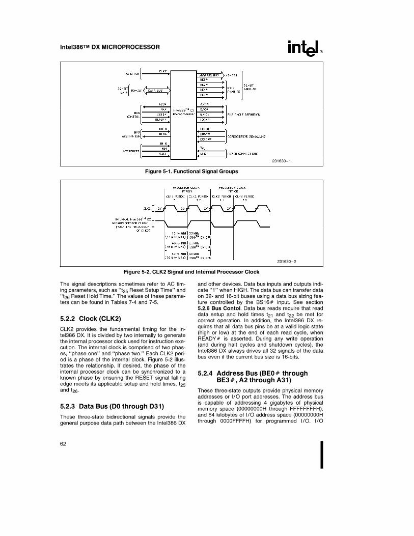
Intel386TM DX MICROPROCESSOR
231630–1
Figure 5-1. Functional Signal Groups
231630–2
Figure 5-2. CLK2 Signal and Internal Processor Clock
The signal descriptions sometimes refer to AC tim-ing parameters, such as ‘‘t25 Reset Setup Time’’ and‘‘t26 Reset Hold Time.’’ The values of these parame-ters can be found in Tables 7-4 and 7-5.
5.2.2 Clock (CLK2)
CLK2 provides the fundamental timing for the In-tel386 DX. It is divided by two internally to generatethe internal processor clock used for instruction exe-cution. The internal clock is comprised of two phas-es, ‘‘phase one’’ and ‘‘phase two.’’ Each CLK2 peri-od is a phase of the internal clock. Figure 5-2 illus-trates the relationship. If desired, the phase of theinternal processor clock can be synchronized to aknown phase by ensuring the RESET signal fallingedge meets its applicable setup and hold times, t25and t26.
5.2.3 Data Bus (D0 through D31)
These three-state bidirectional signals provide thegeneral purpose data path between the Intel386 DX
and other devices. Data bus inputs and outputs indi-cate ‘‘1’’ when HIGH. The data bus can transfer dataon 32- and 16-bit buses using a data bus sizing fea-ture controlled by the BS16Ý input. See section5.2.6 Bus Contol. Data bus reads require that readdata setup and hold times t21 and t22 be met forcorrect operation. In addition, the Intel386 DX re-quires that all data bus pins be at a valid logic state(high or low) at the end of each read cycle, whenREADYÝ is asserted. During any write operation(and during halt cycles and shutdown cycles), theIntel386 DX always drives all 32 signals of the databus even if the current bus size is 16-bits.
5.2.4 Address Bus (BE0Ý throughBE3Ý, A2 through A31)
These three-state outputs provide physical memoryaddresses or I/O port addresses. The address busis capable of addressing 4 gigabytes of physicalmemory space (00000000H through FFFFFFFFH),and 64 kilobytes of I/O address space (00000000Hthrough 0000FFFFH) for programmed I/O. I/O
62

Intel386TM DX MICROPROCESSOR
transfers automatically generated for Intel386 DX-to-coprocessor communication use I/O addresses800000F8H through 800000FFH, so A31 HIGH inconjunction with M/IOÝ LOW allows simple genera-tion of the coprocessor select signal.
The Byte Enable outputs, BE0Ý–BE3Ý, directly in-dicate which bytes of the 32-bit data bus are in-volved with the current transfer. This is most conve-nient for external hardware.
BE0Ý applies to D0–D7BE1Ý applies to D8–D15BE2Ý applies to D16–D23BE3Ý applies to D24–D31
The number of Byte Enables asserted indicates thephysical size of the operand being transferred (1, 2,3, or 4 bytes). Refer to section 5.3.6 Operand Align-ment.
When a memory write cycle or I/O write cycle is inprogress, and the operand being transferred occu-pies only the upper 16 bits of the data bus (D16–D31), duplicate data is simultaneously presented onthe corresponding lower 16-bits of the data bus(D0–D15). This duplication is performed for optimumwrite performance on 16-bit buses. The pattern ofwrite data duplication is a function of the Byte En-ables asserted during the write cycle. Table 5-1 liststhe write data present on D0–D31, as a function ofthe asserted Byte Enable outputs BE0Ý–BE3Ý.
5.2.5 Bus Cycle Definition Signals(W/RÝ, D/CÝ, M/IOÝ, LOCKÝ)
These three-state outputs define the type of bus cy-cle being performed. W/RÝ distinguishes betweenwrite and read cycles. D/CÝ distinguishes betweendata and control cycles. M/IOÝ distinguishes be-tween memory and I/O cycles. LOCKÝ distin-guishes between locked and unlocked bus cycles.
The primary bus cycle definition signals are W/RÝ,D/CÝ and M/IOÝ, since these are the signals driv-en valid as the ADSÝ (Address Status output) isdriven asserted. The LOCKÝ is driven valid at thesame time as the first locked bus cycle begins,which due to address pipelining, could be later thanADSÝ is driven asserted. See 5.4.3.4 Pipelined Ad-dress. The LOCKÝ is negated when the READYÝinput terminates the last bus cycle which waslocked.
Exact bus cycle definitions, as a function of W/RÝ,D/CÝ, and M/IOÝ, are given in Table 5-2. Note onecombination of W/RÝ, D/CÝ and M/IOÝ is nevergiven when ADSÝ is asserted (however, that combi-nation, which is listed as ‘‘does not occur,’’ may oc-cur during idle bus states when ADSÝ is not assert-ed). If M/IOÝ, D/CÝ, and W/RÝ are qualified byADSÝ asserted, then a decoding scheme may besimplified by using this definition of the ‘‘does notoccur’’ combination.
Table 5-1. Write Data Duplication as a Function of BE0Ý–BE3Ý
Intel386TM DX Byte Enables Intel386TM DX Write Data Automatic
BE3Ý BE2Ý BE1Ý BE0Ý D24–D31 D16–D23 D8–D15 D0–D7Duplication?
High High High Low undef undef undef A No
High High Low High undef undef B undef No
High Low High High undef C undef C Yes
Low High High High D undef D undef Yes
High High Low Low undef undef B A No
High Low Low High undef C B undef No
Low Low High High D C D C Yes
High Low Low Low undef C B A No
Low Low Low High D C B undef No
Low Low Low Low D C B A No
Key:
D e logical write data d24–d31
C e logical write data d16–d23
B e logical write data d8–d15
A e logical write data d0–d7
63
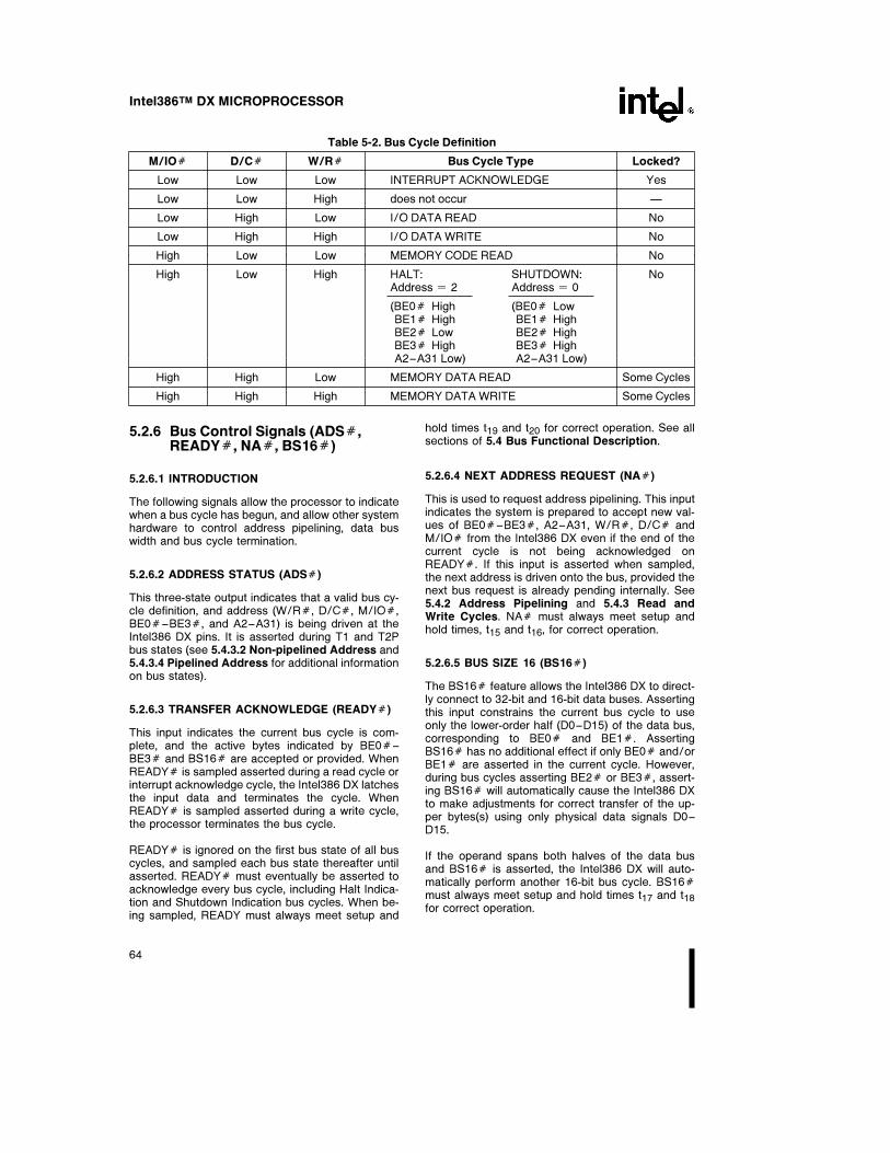
Intel386TM DX MICROPROCESSOR
Table 5-2. Bus Cycle Definition
M/IOÝ D/CÝ W/RÝ Bus Cycle Type Locked?
Low Low Low INTERRUPT ACKNOWLEDGE Yes
Low Low High does not occur Ð
Low High Low I/O DATA READ No
Low High High I/O DATA WRITE No
High Low Low MEMORY CODE READ No
High Low High HALT: SHUTDOWN: NoAddress e 2 Address e 0
(BE0Ý High (BE0Ý LowBE1Ý High BE1Ý HighBE2Ý Low BE2Ý HighBE3Ý High BE3Ý HighA2–A31 Low) A2–A31 Low)
High High Low MEMORY DATA READ Some Cycles
High High High MEMORY DATA WRITE Some Cycles
5.2.6 Bus Control Signals (ADSÝ,READYÝ, NAÝ, BS16Ý)
5.2.6.1 INTRODUCTION
The following signals allow the processor to indicatewhen a bus cycle has begun, and allow other systemhardware to control address pipelining, data buswidth and bus cycle termination.
5.2.6.2 ADDRESS STATUS (ADSÝ)
This three-state output indicates that a valid bus cy-cle definition, and address (W/RÝ, D/CÝ, M/IOÝ,BE0Ý–BE3Ý, and A2–A31) is being driven at theIntel386 DX pins. It is asserted during T1 and T2Pbus states (see 5.4.3.2 Non-pipelined Address and5.4.3.4 Pipelined Address for additional informationon bus states).
5.2.6.3 TRANSFER ACKNOWLEDGE (READYÝ)
This input indicates the current bus cycle is com-plete, and the active bytes indicated by BE0Ý–BE3Ý and BS16Ý are accepted or provided. WhenREADYÝ is sampled asserted during a read cycle orinterrupt acknowledge cycle, the Intel386 DX latchesthe input data and terminates the cycle. WhenREADYÝ is sampled asserted during a write cycle,the processor terminates the bus cycle.
READYÝ is ignored on the first bus state of all buscycles, and sampled each bus state thereafter untilasserted. READYÝ must eventually be asserted toacknowledge every bus cycle, including Halt Indica-tion and Shutdown Indication bus cycles. When be-ing sampled, READY must always meet setup and
hold times t19 and t20 for correct operation. See allsections of 5.4 Bus Functional Description.
5.2.6.4 NEXT ADDRESS REQUEST (NAÝ)
This is used to request address pipelining. This inputindicates the system is prepared to accept new val-ues of BE0Ý–BE3Ý, A2–A31, W/RÝ, D/CÝ andM/IOÝ from the Intel386 DX even if the end of thecurrent cycle is not being acknowledged onREADYÝ. If this input is asserted when sampled,the next address is driven onto the bus, provided thenext bus request is already pending internally. See5.4.2 Address Pipelining and 5.4.3 Read andWrite Cycles. NAÝ must always meet setup andhold times, t15 and t16, for correct operation.
5.2.6.5 BUS SIZE 16 (BS16Ý)
The BS16Ý feature allows the Intel386 DX to direct-ly connect to 32-bit and 16-bit data buses. Assertingthis input constrains the current bus cycle to useonly the lower-order half (D0–D15) of the data bus,corresponding to BE0Ý and BE1Ý. AssertingBS16Ý has no additional effect if only BE0Ý and/orBE1Ý are asserted in the current cycle. However,during bus cycles asserting BE2Ý or BE3Ý, assert-ing BS16Ý will automatically cause the Intel386 DXto make adjustments for correct transfer of the up-per bytes(s) using only physical data signals D0–D15.
If the operand spans both halves of the data busand BS16Ý is asserted, the Intel386 DX will auto-matically perform another 16-bit bus cycle. BS16Ýmust always meet setup and hold times t17 and t18for correct operation.
64

Intel386TM DX MICROPROCESSOR
Intel386 DX I/O cycles are automatically generatedfor coprocessor communication. Since the Intel386DX must transfer 32-bit quantities between itself andthe Intel387 DX, BS16Ý must not be asserted dur-ing Intel387 DX communication cycles.
5.2.7 Bus Arbitration Signals(HOLD, HLDA)
5.2.7.1 INTRODUCTION
This section describes the mechanism by which theprocessor relinquishes control of its local buseswhen requested by another bus master device. See5.5.1 Entering and Exiting Hold Acknowledge foradditional information.
5.2.7.2 BUS HOLD REQUEST (HOLD)
This input indicates some device other than the In-tel386 DX requires bus mastership.
HOLD must remain asserted as long as any otherdevice is a local bus master. HOLD is not recognizedwhile RESET is asserted. If RESET is asserted whileHOLD is asserted, RESET has priority and placesthe bus into an idle state, rather than the hold ac-knowledge (high impedance) state.
HOLD is level-sensitive and is a synchronous input.HOLD signals must always meet setup and holdtimes t23 and t24 for correct operation.
5.2.7.3 BUS HOLD ACKNOWLEDGE (HLDA)
Assertion of this output indicates the Intel386 DXhas relinquished control of its local bus in responseto HOLD asserted, and is in the bus Hold Acknowl-edge state.
The Hold Acknowledge state offers near-completesignal isolation. In the Hold Acknowledge state,HLDA is the only signal being driven by the Intel386DX. The other output signals or bidirectional signals(D0–D31, BE0Ý–BE3Ý, A2–A31, W/RÝ, D/CÝ,M/IOÝ, LOCKÝ and ADSÝ) are in a high-imped-ance state so the requesting bus master may controlthem. Pullup resistors may be desired on several sig-nals to avoid spurious activity when no bus master isdriving them. See 7.2.3 Resistor Recommenda-tions. Also, one rising edge occuring on the NMIinput during Hold Acknowledge is remembered, forprocessing after the HOLD input is negated.
In addition to the normal usage of Hold Acknowl-edge with DMA controllers or master peripherals,
the near-complete isolation has particular attractive-ness during system test when test equipment drivesthe system, and in hardware-fault-tolerant applica-tions.
5.2.8 Coprocessor Interface Signals(PEREQ, BUSYÝ, ERRORÝ)
5.2.8.1 INTRODUCTION
In the following sections are descriptions of signalsdedicated to the numeric coprocessor interface. Inaddition to the data bus, address bus, and bus cycledefinition signals, these following signals controlcommunication between the Intel386 DX and its In-tel387 DX processor extension.
5.2.8.2 COPROCESSOR REQUEST (PEREQ)
When asserted, this input signal indicates a coproc-essor request for a data operand to be transferredto/from memory by the Intel386 DX. In response,the Intel386 DX transfers information between thecoprocessor and memory. Because the Intel386 DXhas internally stored the coprocessor opcode beingexecuted, it performs the requested data transferwith the correct direction and memory address.
PEREQ is level-sensitive and is allowed to be asyn-chronous to the CLK2 signal.
5.2.8.3 COPROCESSOR BUSY (BUSYÝ)
When asserted, this input indicates the coprocessoris still executing an instruction, and is not yet able toaccept another. When the Intel386 DX encountersany coprocessor instruction which operates on thenumeric stack (e.g. load, pop, or arithmetic opera-tion), or the WAIT instruction, this input is first auto-matically sampled until it is seen to be negated. Thissampling of the BUSYÝ input prevents overrunningthe execution of a previous coprocessor instruction.
The FNINIT and FNCLEX coprocessor instructionsare allowed to execute even if BUSYÝ is asserted,since these instructions are used for coprocessorinitialization and exception-clearing.
BUSYÝ is level-sensitive and is allowed to be asyn-chronous to the CLK2 signal.
BUSYÝ serves an additional function. If BUSYÝ issampled LOW at the falling edge of RESET, the In-tel386 DX performs an internal self-test (see 5.5.3Bus Activity During and Following Reset). IfBUSYÝ is sampled HIGH, no self-test is performed.
65

Intel386TM DX MICROPROCESSOR
5.2.8.4 COPROCESSOR ERROR (ERRORÝ)
This input signal indicates that the previous coproc-essor instruction generated a coprocessor error of atype not masked by the coprocessor’s control regis-ter. This input is automatically sampled by the In-tel386 DX when a coprocessor instruction is en-countered, and if asserted, the Intel386 DX gener-ates exception 16 to access the error-handling soft-ware.
Several coprocessor instructions, generally thosewhich clear the numeric error flags in the coproces-sor or save coprocessor state, do execute withoutthe Intel386 DX generating exception 16 even if ER-RORÝ is asserted. These instructions are FNINIT,FNCLEX, FSTSW, FSTSWAX, FSTCW, FSTENV,FSAVE, FESTENV and FESAVE.
ERRORÝ is level-sensitive and is allowed to beasynchronous to the CLK2 signal.
5.2.9 Interrupt Signals (INTR, NMI,RESET)
5.2.9.1 INTRODUCTION
The following descriptions cover inputs that can in-terrupt or suspend execution of the processor’s cur-rent instruction stream.
5.2.9.2 MASKABLE INTERRUPT REQUEST (INTR)
When asserted, this input indicates a request for in-terrupt service, which can be masked by the Intel386DX Flag Register IF bit. When the Intel386 DX re-sponds to the INTR input, it performs two interruptacknowledge bus cycles, and at the end of the sec-ond, latches an 8-bit interrupt vector on D0–D7 toidentify the source of the interrupt.
INTR is level-sensitive and is allowed to be asyn-chronous to the CLK2 signal. To assure recognitionof an INTR request, INTR should remain asserteduntil the first interrupt acknowledge bus cycle be-gins.
5.2.9.3 NON-MASKABLE INTERRUPT REQUEST(NMI)
This input indicates a request for interrupt service,which cannot be masked by software. The non-
maskable interrupt request is always processed ac-cording to the pointer or gate in slot 2 of the interrupttable. Because of the fixed NMI slot assignment, nointerrupt acknowledge cycles are perfomed whenprocessing NMI.
NMI is rising edge-sensitive and is allowed to beasynchronous to the CLK2 signal. To assure recog-nition of NMI, it must be negated for at least eightCLK2 periods, and then be asserted for at leasteight CLK2 periods.
Once NMI processing has begun, no additionalNMI’s are processed until after the next IRET in-struction, which is typically the end of the NMI serv-ice routine. If NMI is re-asserted prior to that time,however, one rising edge on NMI will be remem-bered for processing after executing the next IRETinstruction.
5.2.9.4 RESET (RESET)
This input signal suspends any operation in progressand places the Intel386 DX in a known reset state.The Intel386 DX is reset by asserting RESET for 15or more CLK2 periods (80 or more CLK2 periodsbefore requesting self test). When RESET is assert-ed, all other input pins are ignored, and all other buspins are driven to an idle bus state as shown in Ta-ble 5-3. If RESET and HOLD are both asserted at apoint in time, RESET takes priority even if the In-tel386 DX was in a Hold Acknowledge state prior toRESET asserted.
RESET is level-sensitive and must be synchronousto the CLK2 signal. If desired, the phase of the inter-nal processor clock, and the entire Intel386 DX statecan be completely synchronized to external circuitryby ensuring the RESET signal falling edge meets itsapplicable setup and hold times, t25 and t26.
Table 5-3. Pin State (Bus Idle) During Reset
Pin Name Signal Level During Reset
ADSÝ HighD0–D31 High ImpedanceBE0Ý–BE3Ý LowA2–A31 HighW/RÝ LowD/CÝ HighM/IOÝ LowLOCKÝ HighHLDA Low
66

Intel386TM DX MICROPROCESSOR
5.2.10 Signal Summary
Table 5-4 summarizes the characteristics of all Intel386 DX signals.
Table 5-4. Intel386TM DX Signal Summary
InputOutput
Signal Name Signal FunctionActive Input/ Synch or
High ImpedanceState Output Asynch
During HLDA?to CLK2
CLK2 Clock Ð I Ð Ð
D0–D31 Data Bus High I/O S Yes
BE0Ý–BE3Ý Byte Enables Low O Ð Yes
A2–A31 Address Bus High O Ð Yes
W/RÝ Write-Read Indication High O Ð Yes
D/CÝ Data-Control Indication High O Ð Yes
M/IOÝ Memory-I/O Indication High O Ð Yes
LOCKÝ Bus Lock Indication Low O Ð Yes
ADSÝ Address Status Low O Ð Yes
NAÝ Next Address Request Low I S Ð
BS16Ý Bus Size 16 Low I S Ð
READYÝ Transfer Acknowledge Low I S Ð
HOLD Bus Hold Request High I S Ð
HLDA Bus Hold Acknowledge High O Ð No
PEREQ Coprocessor Request High I A Ð
BUSYÝ Coprocessor Busy Low I A Ð
ERRORÝ Coprocessor Error Low I A Ð
INTR Maskable Interrupt Request High I A Ð
NMI Non-Maskable Intrpt Request High I A Ð
RESET Reset High I S Ð
5.3 BUS TRANSFER MECHANISM
5.3.1 Introduction
All data transfers occur as a result of one or morebus cycles. Logical data operands of byte, word anddouble-word lengths may be transferred without re-strictions on physical address alignment. Any byteboundary may be used, although two or even threephysical bus cycles are performed as required forunaligned operand transfers. See 5.3.4 DynamicData Bus Sizing and 5.3.6 Operand Alignment.
The Intel386 DX address signals are designed tosimplify external system hardware. Higher-order ad-dress bits are provided by A2–A31. Lower-order ad-dress in the form of BE0Ý–BE3Ý directly provideslinear selects for the four bytes of the 32-bit databus. Physical operand size information is thereby im-plicitly provided each bus cycle in the most usableform.
Byte Enable outputs BE0Ý–BE3Ý are assertedwhen their associated data bus bytes are involvedwith the present bus cycle, as listed in Table 5-5.During a bus cycle, any possible pattern of contigu-ous, asserted Byte Enable outputs can occur, butnever patterns having a negated Byte Enable sepa-rating two or three asserted Enables.
67
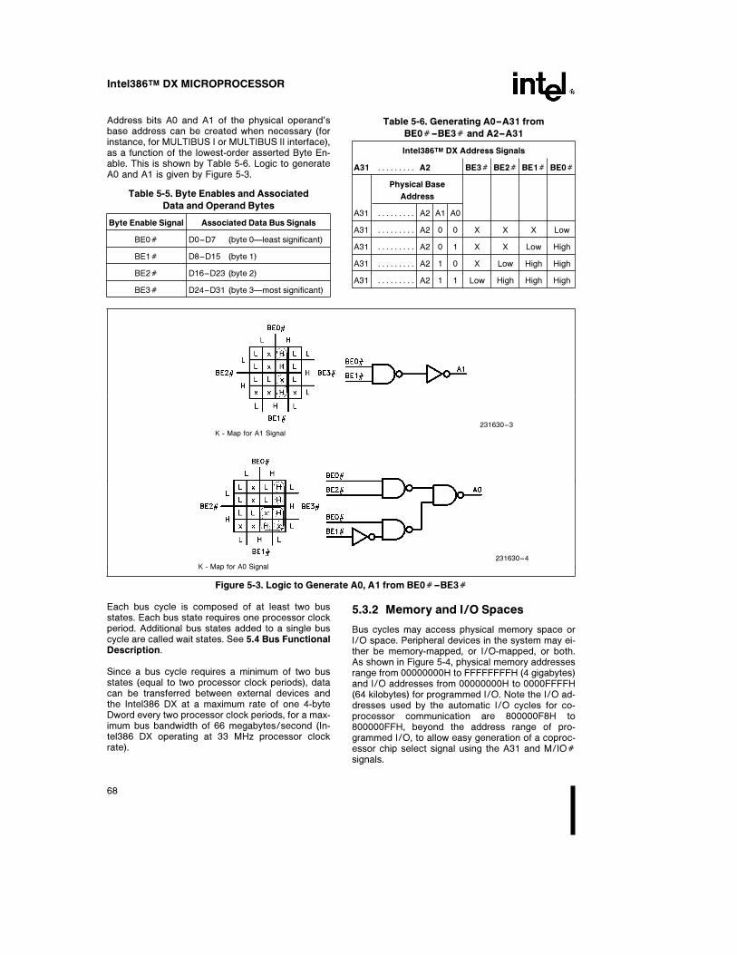
Intel386TM DX MICROPROCESSOR
Address bits A0 and A1 of the physical operand’sbase address can be created when necessary (forinstance, for MULTIBUS I or MULTIBUS II interface),as a function of the lowest-order asserted Byte En-able. This is shown by Table 5-6. Logic to generateA0 and A1 is given by Figure 5-3.
Table 5-5. Byte Enables and Associated
Data and Operand Bytes
Byte Enable Signal Associated Data Bus Signals
BE0Ý D0–D7 (byte 0Ðleast significant)
BE1Ý D8–D15 (byte 1)
BE2Ý D16–D23 (byte 2)
BE3Ý D24–D31 (byte 3Ðmost significant)
Table 5-6. Generating A0–A31 from
BE0Ý–BE3Ý and A2–A31
Intel386TM DX Address Signals
A31 ÀÀÀÀÀÀÀÀÀ A2 BE3Ý BE2Ý BE1Ý BE0Ý
Physical Base
Address
A31 ÀÀÀÀÀÀÀÀÀ A2 A1 A0
A31 ÀÀÀÀÀÀÀÀÀ A2 0 0 X X X Low
A31 ÀÀÀÀÀÀÀÀÀ A2 0 1 X X Low High
A31 ÀÀÀÀÀÀÀÀÀ A2 1 0 X Low High High
A31 ÀÀÀÀÀÀÀÀÀ A2 1 1 Low High High High
231630–3K - Map for A1 Signal
231630–4K - Map for A0 Signal
Figure 5-3. Logic to Generate A0, A1 from BE0Ý–BE3Ý
Each bus cycle is composed of at least two busstates. Each bus state requires one processor clockperiod. Additional bus states added to a single buscycle are called wait states. See 5.4 Bus FunctionalDescription.
Since a bus cycle requires a minimum of two busstates (equal to two processor clock periods), datacan be transferred between external devices andthe Intel386 DX at a maximum rate of one 4-byteDword every two processor clock periods, for a max-imum bus bandwidth of 66 megabytes/second (In-tel386 DX operating at 33 MHz processor clockrate).
5.3.2 Memory and I/O Spaces
Bus cycles may access physical memory space orI/O space. Peripheral devices in the system may ei-ther be memory-mapped, or I/O-mapped, or both.As shown in Figure 5-4, physical memory addressesrange from 00000000H to FFFFFFFFH (4 gigabytes)and I/O addresses from 00000000H to 0000FFFFH(64 kilobytes) for programmed I/O. Note the I/O ad-dresses used by the automatic I/O cycles for co-processor communication are 800000F8H to800000FFH, beyond the address range of pro-grammed I/O, to allow easy generation of a coproc-essor chip select signal using the A31 and M/IOÝsignals.
68

Intel386TM DX MICROPROCESSOR
231630–5Physical Memory Space I/O Space
NOTE:Since A31 is HIGH during automatic communication with coprocessor, A31 HIGH and M/IOÝ LOW can be used toeasily generate a coprocessor select signal.
Figure 5-4. Physical Memory and I/O Spaces
5.3.3 Memory and I/O Organization
The Intel386 DX datapath to memory and I/Ospaces can be 32 bits wide or 16 bits wide. When32-bits wide, memory and I/O spaces are organizednaturally as arrays of physical 32-bit Dwords. Eachmemory or I/O Dword has four individually address-able bytes at consecutive byte addresses. The low-est-addressed byte is associated with data signalsD0–D7; the highest-addressed byte with D24–D31.
The Intel386 DX includes a bus control input,BS16Ý, that also allows direct connection to 16-bitmemory or I/O spaces organized as a sequence of16-bit words. Cycles to 32-bit and 16-bit memory orI/O devices may occur in any sequence, since theBS16Ý control is sampled during each bus cycle.See 5.3.4 Dynamic Data Bus Sizing. The Byte En-able signals, BE0Ý–BE3Ý, allow byte granularitywhen addressing any memory or I/O structure,whether 32 or 16 bits wide.
5.3.4 Dynamic Data Bus Sizing
Dynamic data bus sizing is a feature allowing directprocessor connection to 32-bit or 16-bit data busesfor memory or I/O. A single processor may connectto both size buses. Transfers to or from 32- or 16-bitports are supported by dynamically determining thebus width during each bus cycle. During each buscycle an address decoding circuit or the slave de-
vice itself may assert BS16Ý for 16-bit ports, or ne-gate BS16Ý for 32-bit ports.
With BS16Ý asserted, the processor automaticallyconverts operand transfers larger than 16 bits, ormisaligned 16-bit transfers, into two or three trans-fers as required. All operand transfers physically oc-cur on D0–D15 when BS16Ý is asserted. There-fore, 16-bit memories or I/O devices only connecton data signals D0–D15. No extra transceivers arerequired.
Asserting BS16Ý only affects the processor whenBE2Ý and/or BE3Ý are asserted during the currentcycle. If only D0–D15 are involved with the transfer,asserting BS16Ý has no affect since the transfercan proceed normally over a 16-bit bus whetherBS16Ý is asserted or not. In other words, assertingBS16Ý has no effect when only the lower half of thebus is involved with the current cycle.
There are two types of situations where the proces-sor is affected by asserting BS16Ý, depending onwhich Byte Enables are asserted during the currentbus cycle:
Upper Half Only:Only BE2Ý and/or BE3Ý asserted.
Upper and Lower Half:At least BE1Ý, BE2Ý asserted (and perhapsalso BE0Ý and/or BE3Ý).
69

Intel386TM DX MICROPROCESSOR
Effect of asserting BS16Ý during ‘‘upper half only’’read cycles:
Asserting BS16Ý during ‘‘upper half only’’ readscauses the Intel386 DX to read data on the lower16 bits of the data bus and ignore data on theupper 16 bits of the data bus. Data that wouldhave been read from D16–D31 (as indicated byBE2Ý and BE3Ý) will instead be read from D0–D15 respectively.
Effect of asserting BS16Ý during ‘‘upper half only’’write cycles:
Asserting BS16Ý during ‘‘upper half only’’ writesdoes not affect the Intel386 DX. When only BE2Ýand/or BE3Ý are asserted during a write cyclethe Intel386 DX always duplicates data signalsD16–D31 onto D0–D15 (see Table 5-1). There-fore, no further Intel386 DX action is required toperform these writes on 32-bit or 16-bit buses.
Effect of asserting BS16Ý during ‘‘upper and lowerhalf’’ read cycles:
Asserting BS16Ý during ‘‘upper and lower half’’reads causes the processor to perform two 16-bitread cycles for complete physical operand trans-fer. Bytes 0 and 1 (as indicated by BE0Ý andBE1Ý) are read on the first cycle using D0–D15.Bytes 2 and 3 (as indicated by BE2Ý and BE3Ý)are read during the second cycle, again usingD0–D15. D16–D31 are ignored during both 16-bitcycles. BE0Ý and BE1Ý are always negated dur-ing the second 16-bit cycle (See Figure 5-14, cy-cles 2 and 2a).
Effect of asserting BS16Ý during ‘‘upper and lowerhalf’’ write cycles:
Asserting BS16Ý during ‘‘upper and lower half’’writes causes the Intel386 DX to perform two16-bit write cycles for complete physical operandtransfer. All bytes are available the first write cycleallowing external hardware to receive Bytes 0 and1 (as indicated by BE0Ý and BE1Ý) using D0–D15. On the second cycle the Intel386 DX dupli-cates Bytes 2 and 3 on D0–D15 and Bytes 2 and3 (as indicated by BE2Ý and BE3Ý) are writtenusing D0–D15. BE0Ý and BE1Ý are always neg-ated during the second 16-bit cycle. BS16Ý mustbe asserted during the second 16-bit cycle. SeeFigure 5-14, cycles 1 and 1a.
5.3.5 Interfacing with 32- and 16-BitMemories
In 32-bit-wide physical memories such as Figure 5-5,each physical Dword begins at a byte address that isa multiple of 4. A2–A31 are directly used as a Dwordselect and BE0Ý–BE3Ý as byte selects. BS16Ý isnegated for all bus cycles involving the 32-bit array.
When 16-bit-wide physical arrays are included in thesystem, as in Figure 5-6, each 16-bit physical wordbegins at a address that is a multiple of 2. Note theaddress is decoded, to assert BS16Ý only duringbus cycles involving the 16-bit array. (If desiring to
231630–6
Figure 5-5. Intel386TM DX with 32-Bit Memory
231630–7
Figure 5-6. Intel386TM DX with 32-Bit and 16-Bit Memory
70

Intel386TM DX MICROPROCESSOR
use pipelined address with 16-bit memories thenBE0Ý–BE3Ý and W/RÝ are also decoded to de-termine when BS16Ý should be asserted. See5.4.3.6 Pipelined Address with Dynamic Data BusSizing.)
A2–A31 are directly usable for addressing 32-bitand 16-bit devices. To address 16-bit devices, A1and two byte enable signals are also needed.
To generate an A1 signal and two Byte Enable sig-nals for 16-bit access, BE0Ý–BE3Ý should be de-coded as in Table 5-7. Note certain combinations ofBE0Ý–BE3Ý are never generated by the Intel386DX, leading to ‘‘don’t care’’ conditions in the decod-er. Any BE0Ý–BE3Ý decoder, such as Figure 5-7,may use the non-occurring BE0Ý–BE3Ý combina-tions to its best advantage.
5.3.6 Operand Alignment
With the flexibility of memory addressing on the In-tel386 DX, it is possible to transfer a logical operandthat spans more than one physical Dword or word ofmemory or I/O. Examples are 32-bit Dword
operands beginning at addresses not evenly divisi-ble by 4, or a 16-bit word operand split between twophysical Dwords of the memory array.
Operand alignment and data bus size dictate whenmultiple bus cycles are required. Table 5-8 describesthe transfer cycles generated for all combinations oflogical operand lengths, alignment, and data bus siz-ing. When multiple bus cycles are required to trans-fer a multi-byte logical operand, the highest-orderbytes are transferred first (but if BS16Ý assertedrequires two 16-bit cycles be performed, that part ofthe transfer is low-order first).
5.4 BUS FUNCTIONAL DESCRIPTION
5.4.1 Introduction
The Intel386 DX has separate, parallel buses fordata and address. The data bus is 32-bits in width,and bidirectional. The address bus provides a 32-bitvalue using 30 signals for the 30 upper-order ad-dress bits and 4 Byte Enable signals to directly indi-cate the active bytes. These buses are interpretedand controlled via several associated definition orcontrol signals.
Table 5-7. Generating A1, BHEÝ and BLEÝ for Addressing 16-Bit Devices
Intel386TM DX Signals 16-Bit Bus SignalsComments
BE3Ý BE2Ý BE1Ý BE0Ý A1 BHEÝ BLEÝ (A0)
H* H* H* H* x x x xÐno active bytesH H H L L H LH H L H L L HH H L L L L LH L H H H H LH* L* H* L* x x x xÐnot contiguous bytesH L L H L L HH L L L L L LL H H H H L HL* H* H* L* x x x xÐnot contiguous bytesL* H* L* H* x x x xÐnot contiguous bytesL* H* L* L* x x x xÐnot contiguous bytesL L H H H L LL* L* H* L* x x x xÐnot continguous bytesL L L H L L HL L L L L L L
BLEÝ asserted when D0–D7 of 16-bit bus is active.BHEÝ asserted when D8–D15 of 16-bit bus is active.A1 low for all even words; A1 high for all odd words.
Key:x e don’t careH e high voltage levelL e low voltage level* e a non-occurring pattern of Byte Enables; either none are asserted,
or the pattern has Byte Enables asserted for non-contiguous bytes
71
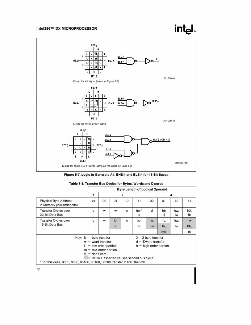
Intel386TM DX MICROPROCESSOR
231630–8K-map for A1 signal (same as Figure 5-3)
231630–9K-map for 16-bit BHEÝ signal
231630–10K-map for 16-bit BLEÝ signal (same as A0 signal in Figure 5-3)
Figure 5-7. Logic to Generate A1, BHEÝ and BLEÝ for 16-Bit Buses
Table 5-8. Transfer Bus Cycles for Bytes, Words and Dwords
Byte-Length of Logical Operand
1 2 4
Physical Byte Address xx 00 01 10 11 00 01 10 11
in Memory (low-order bits)
Transfer Cycles over b w w w hb,* d hb hw, h3,
32-Bit Data Bus lb l3 lw lb
Transfer Cycles over b w lb, w hb, lw, hb, hw, mw,
16-Bit Data Bushb lb hw lb, lw hb,
mw lb
Key: b e byte transfer 3 e3-byte transfer
w e word transfer d e Dword transfer
l e low-order portion h e high-order portion
m e mid-order portion
x e don’t caree BS16Ý asserted causes second bus cycle
*For this case, 8086, 8088, 80186, 80188, 80286 transfer lb first, then hb.
72

Intel386TM DX MICROPROCESSOR
The definition of each bus cycle is given by threedefinition signals: M/IOÝ, W/RÝ and D/CÝ. At thesame time, a valid address is present on the byteenable signals BE0Ý–BE3Ý and other address sig-nals A2–A31. A status signal, ADSÝ, indicateswhen the Intel386 DX issues a new bus cycle defini-tion and address.
Collectively, the address bus, data bus and all asso-ciated control signals are referred to simply as ‘‘thebus’’.
When active, the bus performs one of the bus cyclesbelow:
1) read from memory space
2) locked read from memory space
3) write to memory space
4) locked write to memory space
5) read from I/O space (or coprocessor)
6) write to I/O space (or coprocessor)
7) interrupt acknowledge
8) indicate halt, or indicate shutdown
Table 5-2 shows the encoding of the bus cycle defi-nition signals for each bus cycle. See section 5.2.5Bus Cycle Definition.
The data bus has a dynamic sizing feature support-ing 32- and 16-bit bus size. Data bus size is indicatedto the Intel386 DX using its Bus Size 16 (BS16Ý)input. All bus functions can be performed with eitherdata bus size.
When the Intel386 DX bus is not performing one ofthe activities listed above, it is either Idle or in theHold Acknowledge state, which may be detected byexternal circuitry. The idle state can be identified bythe Intel386 DX giving no further assertions on itsaddress strobe output (ADSÝ) since the beginningof its most recent bus cycle, and the most recentbus cycle has been terminated. The hold acknowl-edge state is identified by the Intel386 DX assertingits hold acknowledge (HLDA) output.
The shortest time unit of bus activity is a bus state. Abus state is one processor clock period (two CLK2periods) in duration. A complete data transfer occursduring a bus cycle, composed of two or more busstates.
231630–11Fastest non-pipelined bus cycles consist of T1 and T2
Figure 5-8. Fastest Read Cycles with Non-Pipelined Address Timing
73
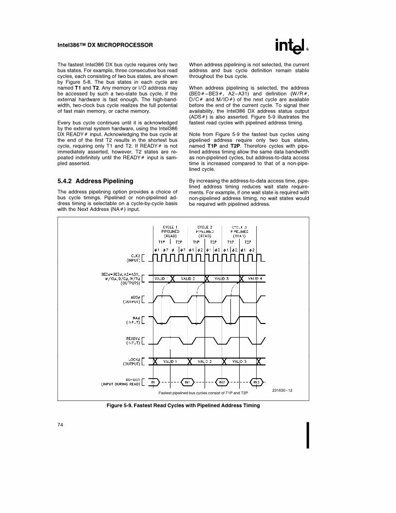
Intel386TM DX MICROPROCESSOR
The fastest Intel386 DX bus cycle requires only twobus states. For example, three consecutive bus readcycles, each consisting of two bus states, are shownby Figure 5-8. The bus states in each cycle arenamed T1 and T2. Any memory or I/O address maybe accessed by such a two-state bus cycle, if theexternal hardware is fast enough. The high-band-width, two-clock bus cycle realizes the full potentialof fast main memory, or cache memory.
Every bus cycle continues until it is acknowledgedby the external system hardware, using the Intel386DX READYÝ input. Acknowledging the bus cycle atthe end of the first T2 results in the shortest buscycle, requiring only T1 and T2. If READYÝ is notimmediately asserted, however, T2 states are re-peated indefinitely until the READYÝ input is sam-pled asserted.
5.4.2 Address Pipelining
The address pipelining option provides a choice ofbus cycle timings. Pipelined or non-pipelined ad-dress timing is selectable on a cycle-by-cycle basiswith the Next Address (NAÝ) input.
When address pipelining is not selected, the currentaddress and bus cycle definition remain stablethroughout the bus cycle.
When address pipelining is selected, the address(BE0Ý–BE3Ý, A2–A31) and definition (W/RÝ,D/CÝ and M/IOÝ) of the next cycle are availablebefore the end of the current cycle. To signal theiravailability, the Intel386 DX address status output(ADSÝ) is also asserted. Figure 5-9 illustrates thefastest read cycles with pipelined address timing.
Note from Figure 5-9 the fastest bus cycles usingpipelined address require only two bus states,named T1P and T2P. Therefore cycles with pipe-lined address timing allow the same data bandwidthas non-pipelined cycles, but address-to-data accesstime is increased compared to that of a non-pipe-lined cycle.
By increasing the address-to-data access time, pipe-lined address timing reduces wait state require-ments. For example, if one wait state is required withnon-pipelined address timing, no wait states wouldbe required with pipelined address.
231630–12Fastest pipelined bus cycles consist of T1P and T2P
Figure 5-9. Fastest Read Cycles with Pipelined Address Timing
74

Intel386TM DX MICROPROCESSOR
Pipelined address timing is useful in typical systemshaving address latches. In those systems, once anaddress has been latched, pipelined availability ofthe next address allows decoding circuitry to gener-ate chip selects (and other necessary select signals)in advance, so selected devices are accessed im-mediately when the next cycle begins. In otherwords, the decode time for the next cycle can beoverlapped with the end of the current cycle.
If a system contains a memory structure of two ormore interleaved memory banks, pipelined addresstiming potentially allows even more overlap of activi-ty. This is true when the interleaved memory control-ler is designed to allow the next memory operation
to begin in one memory bank while the current buscycle is still activating another memory bank. Figure5-10 shows the general structure of the Intel386 DXwith 2-bank and 4-bank interleaved memory. Noteeach memory bank of the interleaved memory hasfull data bus width (32-bit data width typically, unless16-bit bus size is selected).
Further details of pipelined address timing are givenin 5.4.3.4 Pipelined Address, 5.4.3.5 Initiating andMaintaining Pipelined Address, 5.4.3.6 PipelinedAddress with Dynamic Bus Sizing, and 5.4.3.7Maximum Pipelined Address Usage with 16-BitBus Size.
TWO-BANK INTERLEAVED MEMORY
a) Address signal A2 selects bank
b) 32-bit datapath to each bank
231630–13
FOUR-BANK INTERLEAVED MEMORY
a) Address signals A3 and A2 select bank
b) 32-bit datapath to each bank
231630–14
Figure 5-10. 2-Bank and 4-Bank Interleaved Memory Structure
75
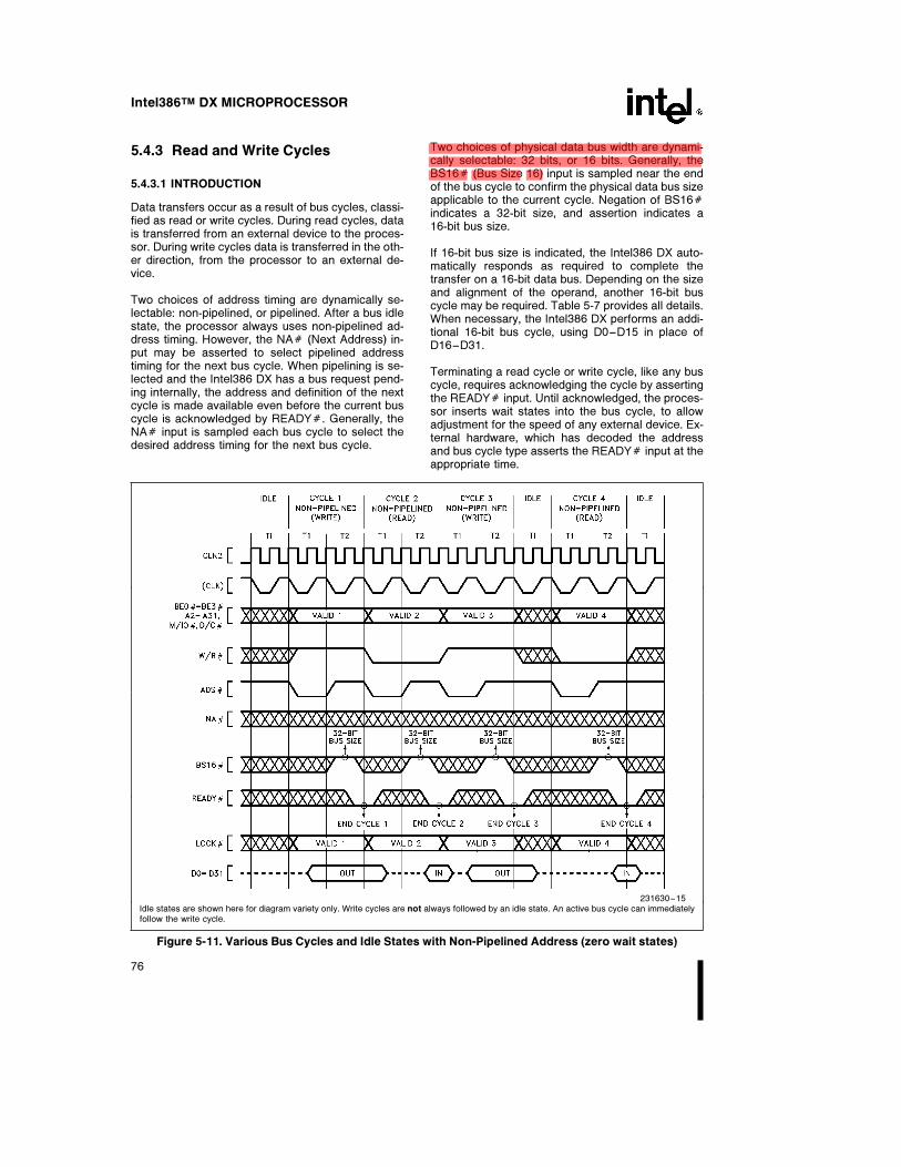
Intel386TM DX MICROPROCESSOR
5.4.3 Read and Write Cycles
5.4.3.1 INTRODUCTION
Data transfers occur as a result of bus cycles, classi-fied as read or write cycles. During read cycles, datais transferred from an external device to the proces-sor. During write cycles data is transferred in the oth-er direction, from the processor to an external de-vice.
Two choices of address timing are dynamically se-lectable: non-pipelined, or pipelined. After a bus idlestate, the processor always uses non-pipelined ad-dress timing. However, the NAÝ (Next Address) in-put may be asserted to select pipelined addresstiming for the next bus cycle. When pipelining is se-lected and the Intel386 DX has a bus request pend-ing internally, the address and definition of the nextcycle is made available even before the current buscycle is acknowledged by READYÝ. Generally, theNAÝ input is sampled each bus cycle to select thedesired address timing for the next bus cycle.
Two choices of physical data bus width are dynami-cally selectable: 32 bits, or 16 bits. Generally, theBS16Ý (Bus Size 16) input is sampled near the endof the bus cycle to confirm the physical data bus sizeapplicable to the current cycle. Negation of BS16Ýindicates a 32-bit size, and assertion indicates a16-bit bus size.
If 16-bit bus size is indicated, the Intel386 DX auto-matically responds as required to complete thetransfer on a 16-bit data bus. Depending on the sizeand alignment of the operand, another 16-bit buscycle may be required. Table 5-7 provides all details.When necessary, the Intel386 DX performs an addi-tional 16-bit bus cycle, using D0–D15 in place ofD16–D31.
Terminating a read cycle or write cycle, like any buscycle, requires acknowledging the cycle by assertingthe READYÝ input. Until acknowledged, the proces-sor inserts wait states into the bus cycle, to allowadjustment for the speed of any external device. Ex-ternal hardware, which has decoded the addressand bus cycle type asserts the READYÝ input at theappropriate time.
231630–15Idle states are shown here for diagram variety only. Write cycles are not always followed by an idle state. An active bus cycle can immediatelyfollow the write cycle.
Figure 5-11. Various Bus Cycles and Idle States with Non-Pipelined Address (zero wait states)
76

Intel386TM DX MICROPROCESSOR
At the end of the second bus state within the buscycle, READYÝ is sampled. At that time, if externalhardware acknowledges the bus cycle by assertingREADYÝ, the bus cycle terminates as shown in Fig-ure 5-11. If READYÝ is negated as in Figure 5-12,the cycle continues another bus state (a wait state)and READYÝ is sampled again at the end of thatstate. This continues indefinitely until the cycle is ac-knowledged by READYÝ asserted.
When the current cycle is acknowledged, the In-tel386 DX terminates it. When a read cycle is ac-knowledged, the Intel386 DX latches the informationpresent at its data pins. When a write cycle is ac-knowledged, the Intel386 DX write data remains val-id throughout phase one of the next bus state, toprovide write data hold time.
5.4.3.2 NON-PIPELINED ADDRESS
Any bus cycle may be performed with non-pipelinedaddress timing. For example, Figure 5-11 shows amixture of read and write cycles with non-pipelinedaddress timing. Figure 5-11 shows the fastest possi-
ble cycles with non-pipelined address have two busstates per bus cycle. The states are named T1 andT2. In phase one of the T1, the address signals andbus cycle definition signals are driven valid, and tosignal their availability, address status (ADSÝ) issimultaneously asserted.
During read or write cycles, the data bus behaves asfollows. If the cycle is a read, the Intel386 DX floatsits data signals to allow driving by the external de-vice being addressed. The Intel386 DX requiresthat all data bus pins be at a valid logic state(high or low) at the end of each read cycle, whenREADYÝ is asserted, even if all byte enables arenot asserted. The system MUST be designed tomeet this requirement. If the cycle is a write, datasignals are driven by the Intel386 DX beginning inphase two of T1 until phase one of the bus statefollowing cycle acknowledgment.
Figure 5-12 illustrates non-pipelined bus cycles withone wait added to cycles 2 and 3. READYÝ is sam-pled negated at the end of the first T2 in cycles 2and 3. Therefore cycles 2 and 3 have T2 repeated.At the end of the second T2, READYÝ is sampledasserted.
231630–16Idle states are shown here for diagram variety only. Write cycles are not always followed by an idle state. An active bus cycle can immediatelyfollow the write cycle.
Figure 5-12. Various Bus Cycles and Idle States with Non-Pipelined Address
(various number of wait states)
77
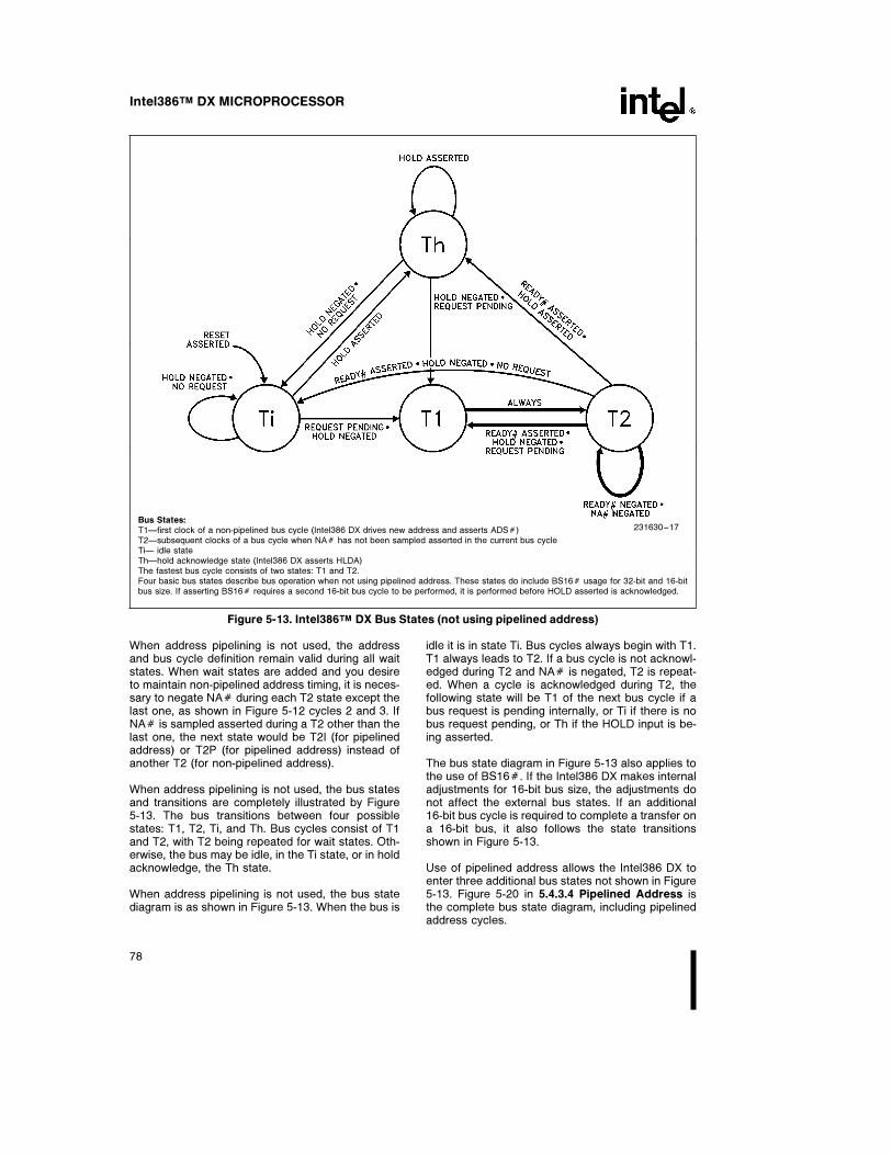
Intel386TM DX MICROPROCESSOR
Bus States:231630–17T1Ðfirst clock of a non-pipelined bus cycle (Intel386 DX drives new address and asserts ADSÝ)
T2Ðsubsequent clocks of a bus cycle when NAÝ has not been sampled asserted in the current bus cycleTiÐ idle stateThÐhold acknowledge state (Intel386 DX asserts HLDA)The fastest bus cycle consists of two states: T1 and T2.Four basic bus states describe bus operation when not using pipelined address. These states do include BS16Ý usage for 32-bit and 16-bitbus size. If asserting BS16Ý requires a second 16-bit bus cycle to be performed, it is performed before HOLD asserted is acknowledged.
Figure 5-13. Intel386TM DX Bus States (not using pipelined address)
When address pipelining is not used, the addressand bus cycle definition remain valid during all waitstates. When wait states are added and you desireto maintain non-pipelined address timing, it is neces-sary to negate NAÝ during each T2 state except thelast one, as shown in Figure 5-12 cycles 2 and 3. IfNAÝ is sampled asserted during a T2 other than thelast one, the next state would be T2I (for pipelinedaddress) or T2P (for pipelined address) instead ofanother T2 (for non-pipelined address).
When address pipelining is not used, the bus statesand transitions are completely illustrated by Figure5-13. The bus transitions between four possiblestates: T1, T2, Ti, and Th. Bus cycles consist of T1and T2, with T2 being repeated for wait states. Oth-erwise, the bus may be idle, in the Ti state, or in holdacknowledge, the Th state.
When address pipelining is not used, the bus statediagram is as shown in Figure 5-13. When the bus is
idle it is in state Ti. Bus cycles always begin with T1.T1 always leads to T2. If a bus cycle is not acknowl-edged during T2 and NAÝ is negated, T2 is repeat-ed. When a cycle is acknowledged during T2, thefollowing state will be T1 of the next bus cycle if abus request is pending internally, or Ti if there is nobus request pending, or Th if the HOLD input is be-ing asserted.
The bus state diagram in Figure 5-13 also applies tothe use of BS16Ý. If the Intel386 DX makes internaladjustments for 16-bit bus size, the adjustments donot affect the external bus states. If an additional16-bit bus cycle is required to complete a transfer ona 16-bit bus, it also follows the state transitionsshown in Figure 5-13.
Use of pipelined address allows the Intel386 DX toenter three additional bus states not shown in Figure5-13. Figure 5-20 in 5.4.3.4 Pipelined Address isthe complete bus state diagram, including pipelinedaddress cycles.
78

Intel386TM DX MICROPROCESSOR
5.4.3.3 NON-PIPELINED ADDRESS WITHDYNAMIC DATA BUS SIZING
The physical data bus width for any non-pipelinedbus cycle can be either 32-bits or 16-bits. At thebeginning of the bus cycle, the processor behavesas if the data bus is 32-bits wide. When the bus cy-cle is acknowledged, by asserting READYÝ at theend of a T2 state, the most recent sampling ofBS16Ý determines the data bus size for the cyclebeing acknowledged. If BS16Ý was most recentlynegated, the physical data bus size is defined as
32 bits. If BS16Ý was most recently asserted, thesize is defined as 16 bits.
When BS16Ý is asserted and two 16-bit bus cyclesare required to complete the transfer, BS16Ý mustbe asserted during the second cycle; 16-bit bus sizeis not assumed. Like any bus cycle, the second16-bit cycle must be acknowledged by assertingREADYÝ.
When a second 16-bit bus cycle is required to com-plete the transfer over a 16-bit bus, the addresses
Key: Dn e physical data pin n 231630–18dn e logical data bit n
Figure 5-14. Asserting BS16Ý (zero wait states, non-pipelined address)
79

Intel386TM DX MICROPROCESSOR
Key: Dn e physical data pin n 231630–19dn e logical data bit n
Figure 5-15. Asserting BS16Ý (one wait state, non-pipelined address)
generated for the two 16-bit bus cycles are closelyrelated to each other. The addresses are the sameexcept BE0Ý and BE1Ý are always negated for thesecond cycle. This is because data on D0–D15 wasalready transferred during the first 16-bit cycle.
Figures 5-14 and 5-15 show cases where assertionof BS16Ý requires a second 16-bit cycle for com-plete operand transfer. Figure 5-14 illustrates cycleswithout wait states. Figure 5-15 illustrates cycleswith one wait state. In Figure 5-15 cycle 1, the bus
cycle during which BS16Ý is asserted, note thatNAÝ must be negated in the T2 state(s) prior to thelast T2 state. This is to allow the recognition ofBS16Ý asserted in the final T2 state. Also note thatduring this state BS16Ý must be stable (defined byt17 and t18, BS16Ý setup and hold timings), in orderto prevent potential data corruption during split cyclereads. The logic state of BS16Ý during this time isnot important. The relation of NAÝ and BS16Ý isgiven fully in 5.4.3.4 Pipelined Address, but Figure5-15 illustrates these precautions you need to knowwhen using BS16Ý with non-pipelined address.
80
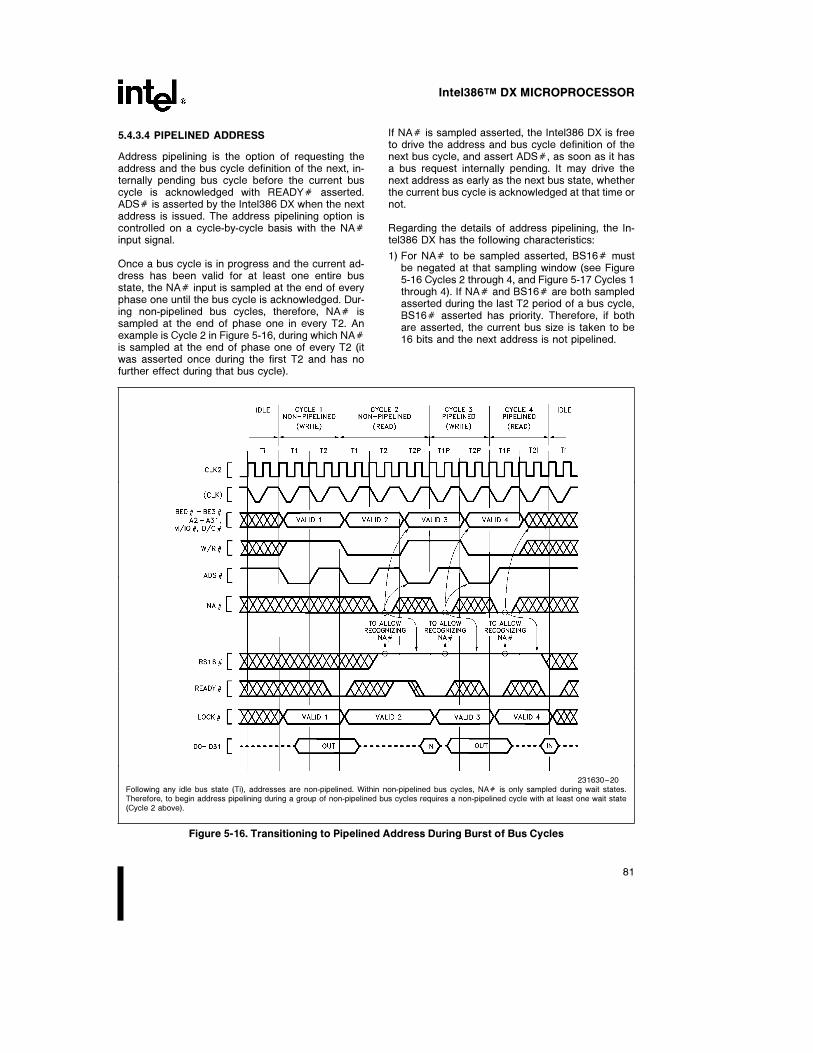
Intel386TM DX MICROPROCESSOR
5.4.3.4 PIPELINED ADDRESS
Address pipelining is the option of requesting theaddress and the bus cycle definition of the next, in-ternally pending bus cycle before the current buscycle is acknowledged with READYÝ asserted.ADSÝ is asserted by the Intel386 DX when the nextaddress is issued. The address pipelining option iscontrolled on a cycle-by-cycle basis with the NAÝinput signal.
Once a bus cycle is in progress and the current ad-dress has been valid for at least one entire busstate, the NAÝ input is sampled at the end of everyphase one until the bus cycle is acknowledged. Dur-ing non-pipelined bus cycles, therefore, NAÝ issampled at the end of phase one in every T2. Anexample is Cycle 2 in Figure 5-16, during which NAÝis sampled at the end of phase one of every T2 (itwas asserted once during the first T2 and has nofurther effect during that bus cycle).
If NAÝ is sampled asserted, the Intel386 DX is freeto drive the address and bus cycle definition of thenext bus cycle, and assert ADSÝ, as soon as it hasa bus request internally pending. It may drive thenext address as early as the next bus state, whetherthe current bus cycle is acknowledged at that time ornot.
Regarding the details of address pipelining, the In-tel386 DX has the following characteristics:
1) For NAÝ to be sampled asserted, BS16Ý mustbe negated at that sampling window (see Figure5-16 Cycles 2 through 4, and Figure 5-17 Cycles 1through 4). If NAÝ and BS16Ý are both sampledasserted during the last T2 period of a bus cycle,BS16Ý asserted has priority. Therefore, if bothare asserted, the current bus size is taken to be16 bits and the next address is not pipelined.
231630–20Following any idle bus state (Ti), addresses are non-pipelined. Within non-pipelined bus cycles, NAÝ is only sampled during wait states.Therefore, to begin address pipelining during a group of non-pipelined bus cycles requires a non-pipelined cycle with at least one wait state(Cycle 2 above).
Figure 5-16. Transitioning to Pipelined Address During Burst of Bus Cycles
81
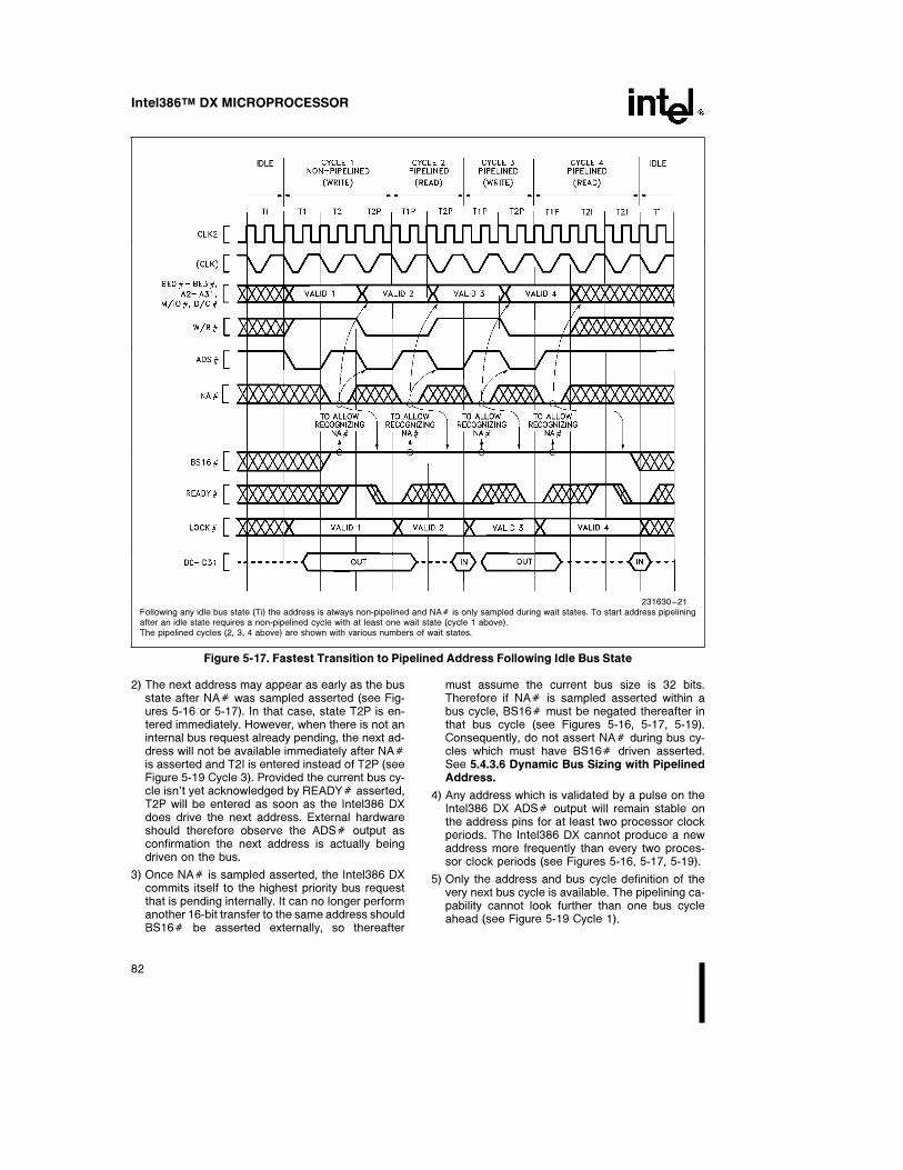
Intel386TM DX MICROPROCESSOR
231630–21Following any idle bus state (Ti) the address is always non-pipelined and NAÝ is only sampled during wait states. To start address pipeliningafter an idle state requires a non-pipelined cycle with at least one wait state (cycle 1 above).The pipelined cycles (2, 3, 4 above) are shown with various numbers of wait states.
Figure 5-17. Fastest Transition to Pipelined Address Following Idle Bus State
2) The next address may appear as early as the busstate after NAÝ was sampled asserted (see Fig-ures 5-16 or 5-17). In that case, state T2P is en-tered immediately. However, when there is not aninternal bus request already pending, the next ad-dress will not be available immediately after NAÝis asserted and T2I is entered instead of T2P (seeFigure 5-19 Cycle 3). Provided the current bus cy-cle isn’t yet acknowledged by READYÝ asserted,T2P will be entered as soon as the Intel386 DXdoes drive the next address. External hardwareshould therefore observe the ADSÝ output asconfirmation the next address is actually beingdriven on the bus.
3) Once NAÝ is sampled asserted, the Intel386 DXcommits itself to the highest priority bus requestthat is pending internally. It can no longer performanother 16-bit transfer to the same address shouldBS16Ý be asserted externally, so thereafter
must assume the current bus size is 32 bits.Therefore if NAÝ is sampled asserted within abus cycle, BS16Ý must be negated thereafter inthat bus cycle (see Figures 5-16, 5-17, 5-19).Consequently, do not assert NAÝ during bus cy-cles which must have BS16Ý driven asserted.See 5.4.3.6 Dynamic Bus Sizing with PipelinedAddress.
4) Any address which is validated by a pulse on theIntel386 DX ADSÝ output will remain stable onthe address pins for at least two processor clockperiods. The Intel386 DX cannot produce a newaddress more frequently than every two proces-sor clock periods (see Figures 5-16, 5-17, 5-19).
5) Only the address and bus cycle definition of thevery next bus cycle is available. The pipelining ca-pability cannot look further than one bus cycleahead (see Figure 5-19 Cycle 1).
82

Intel386TM DX MICROPROCESSOR
The complete bus state transition diagram, includingoperation with pipelined address is given by 5-20.Note it is a superset of the diagram for non-pipelinedaddress only, and the three additional bus states forpipelined address are drawn in bold.
The fastest bus cycle with pipelined address con-sists of just two bus states, T1P and T2P (recall fornon-pipelined address it is T1 and T2). T1P is thefirst bus state of a pipelined cycle.
5.4.3.5 INITIATING AND MAINTAININGPIPELINED ADDRESS
Using the state diagram Figure 5-20, observe thetransitions from an idle state, Ti, to the beginning ofa pipelined bus cycle, T1P. From an idle state Ti, thefirst bus cycle must begin with T1, and is therefore anon-pipelined bus cycle. The next bus cycle will bepipelined, however, provided NAÝ is asserted andthe first bus cycle ends in a T2P state (the addressfor the next bus cycle is driven during T2P). The fast-est path from an idle state to a bus cycle with pipe-lined address is shown in bold below:
Ti, Ti, Ti T1 - T2 - T2P, T1P - T2P,X ä Y X ä Y X ä Yidle non-pipelined pipelined
states cycle cycle
T1-T2-T2P are the states of the bus cycle that es-tablishes address pipelining for the next bus cycle,which begins with T1P. The same is true after a bushold state, shown below:
Th, Th, Th, T1 - T2 - T2P, T1P - T2P,X ä YX ä Y X ä Yhold non-pipelined pipelined
acknowledge cycle cyclestates
The transition to pipelined address is shown func-tionally by Figure 5-17 Cycle 1. Note that Cycle 1 isused to transition into pipelined address timing forthe subsequent Cycles 2, 3 and 4, which are pipe-lined. The NAÝ input is asserted at the appropriatetime to select address pipelining for Cycles 2, 3and 4.
Once a bus cycle is in progress and the current ad-dress has become valid, the NAÝ input is sampledat the end of every phase one, beginning with thenext bus state, until the bus cycle is acknowledged.During Figure 5-17 Cycle 1 therefore, sampling be-gins in T2. Once NAÝ is sampled asserted duringthe current cycle, the Intel386 DX is free to drive anew address and bus cycle definition on the bus asearly as the next bus state. In Figure 5-16 Cycle 1 forexample, the next address is driven during stateT2P. Thus Cycle 1 makes the transition to pipelinedaddress timing, since it begins with T1 but ends withT2P. Because the address for Cycle 2 is availablebefore Cycle 2 begins, Cycle 2 is called a pipelinedbus cycle, and it begins with T1P. Cycle 2 begins assoon as READYÝ asserted terminates Cycle 1.
Example transition bus cycles are Figure 5-17 Cycle1 and Figure 5-16 Cycle 2. Figure 5-17 shows tran-sition during the very first cycle after an idle busstate, which is the fastest possible transition into ad-dress pipelining. Figure 5-16 Cycle 2 shows a tran-sition cycle occurring during a burst of bus cycles. Inany case, a transition cycle is the same whenever itoccurs: it consists at least of T1, T2 (you assertNAÝ at that time), and T2P (provided the Intel386DX has an internal bus request already pending,which it almost always has). T2P states are repeatedif wait states are added to the cycle.
Note three states (T1, T2 and T2P) are only requiredin a bus cycle performing a transition from non-pipelined address into pipelined address timing, forexample Figure 5-17 Cycle 1. Figure 5-17 Cycles 2,3 and 4 show that address pipelining can be main-tained with two-state bus cycles consisting only ofT1P and T2P.
Once a pipelined bus cycle is in progress, pipelinedtiming is maintained for the next cycle by assertingNAÝ and detecting that the Intel386 DX enters T2Pduring the current bus cycle. The current bus cyclemust end in state T2P for pipelining to be maintainedin the next cycle. T2P is identified by the assertion ofADSÝ. Figures 5-16 and 5-17 however, each showpipelining ending after Cycle 4 because Cycle 4ends in T2I. This indicates the Intel386 DX didn’thave an internal bus request prior to the acknowl-edgement of Cycle 4. If a cycle ends with a T2 orT2I, the next cycle will not be pipelined.
83

Intel386TM DX MICROPROCESSOR
231630–23
Figure 5-19. Details of Address Pipelining During Cycles with Wait States
84
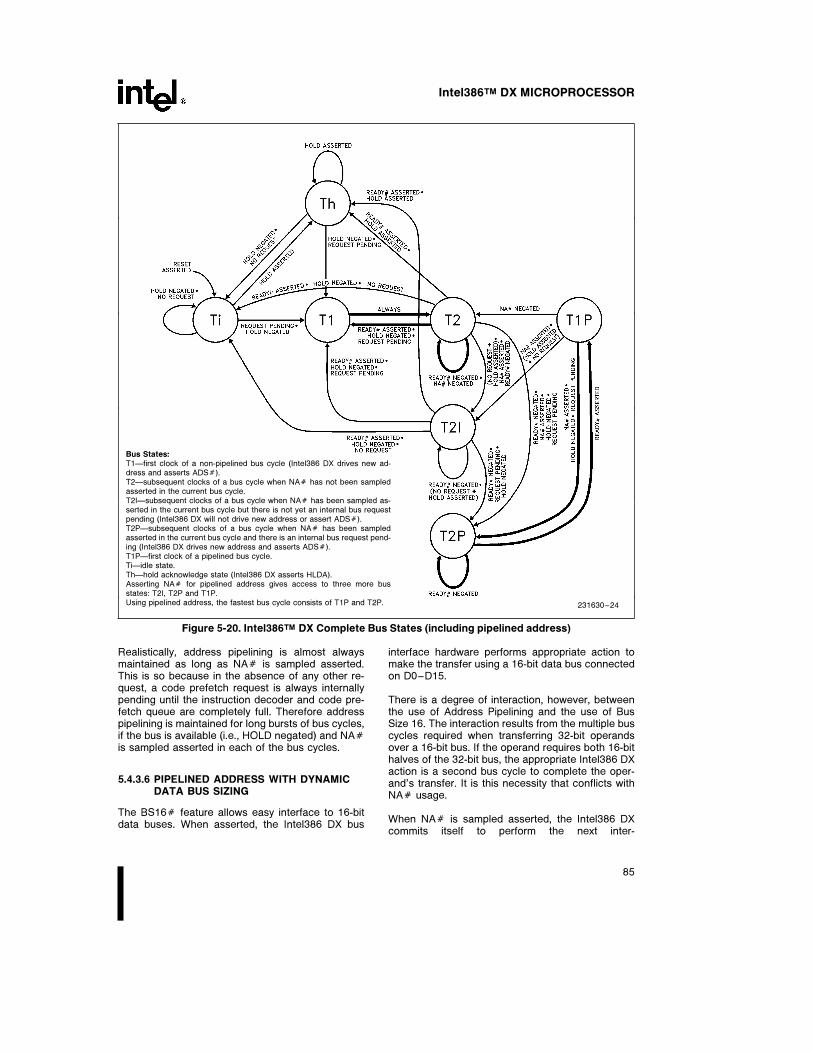
Intel386TM DX MICROPROCESSOR
Bus States:T1Ðfirst clock of a non-pipelined bus cycle (Intel386 DX drives new ad-dress and asserts ADSÝ).T2Ðsubsequent clocks of a bus cycle when NAÝ has not been sampledasserted in the current bus cycle.T2IÐsubsequent clocks of a bus cycle when NAÝ has been sampled as-serted in the current bus cycle but there is not yet an internal bus requestpending (Intel386 DX will not drive new address or assert ADSÝ).T2PÐsubsequent clocks of a bus cycle when NAÝ has been sampledasserted in the current bus cycle and there is an internal bus request pend-ing (Intel386 DX drives new address and asserts ADSÝ).T1PÐfirst clock of a pipelined bus cycle.TiÐidle state.ThÐhold acknowledge state (Intel386 DX asserts HLDA).Asserting NAÝ for pipelined address gives access to three more busstates: T2I, T2P and T1P.Using pipelined address, the fastest bus cycle consists of T1P and T2P. 231630–24
Figure 5-20. Intel386TM DX Complete Bus States (including pipelined address)
Realistically, address pipelining is almost alwaysmaintained as long as NAÝ is sampled asserted.This is so because in the absence of any other re-quest, a code prefetch request is always internallypending until the instruction decoder and code pre-fetch queue are completely full. Therefore addresspipelining is maintained for long bursts of bus cycles,if the bus is available (i.e., HOLD negated) and NAÝis sampled asserted in each of the bus cycles.
5.4.3.6 PIPELINED ADDRESS WITH DYNAMICDATA BUS SIZING
The BS16Ý feature allows easy interface to 16-bitdata buses. When asserted, the Intel386 DX bus
interface hardware performs appropriate action tomake the transfer using a 16-bit data bus connectedon D0–D15.
There is a degree of interaction, however, betweenthe use of Address Pipelining and the use of BusSize 16. The interaction results from the multiple buscycles required when transferring 32-bit operandsover a 16-bit bus. If the operand requires both 16-bithalves of the 32-bit bus, the appropriate Intel386 DXaction is a second bus cycle to complete the oper-and’s transfer. It is this necessity that conflicts withNAÝ usage.
When NAÝ is sampled asserted, the Intel386 DXcommits itself to perform the next inter-
85
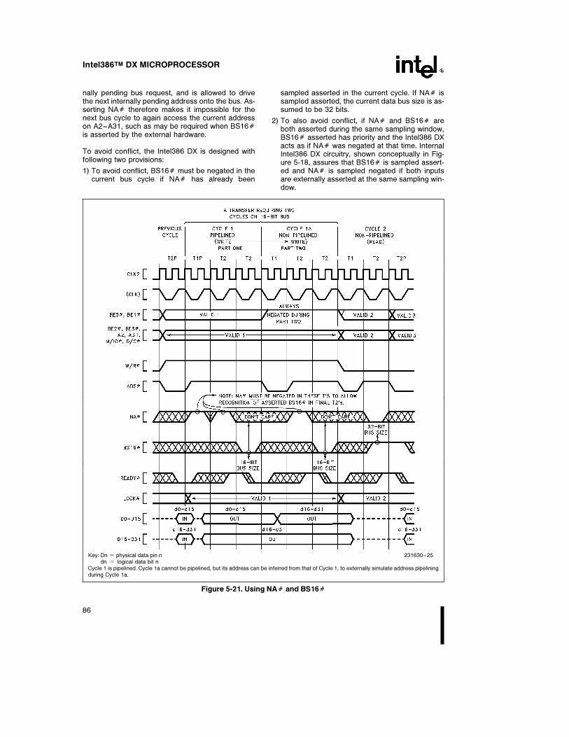
Intel386TM DX MICROPROCESSOR
nally pending bus request, and is allowed to drivethe next internally pending address onto the bus. As-serting NAÝ therefore makes it impossible for thenext bus cycle to again access the current addresson A2–A31, such as may be required when BS16Ýis asserted by the external hardware.
To avoid conflict, the Intel386 DX is designed withfollowing two provisions:
1) To avoid conflict, BS16Ý must be negated in thecurrent bus cycle if NAÝ has already been
sampled asserted in the current cycle. If NAÝ issampled asserted, the current data bus size is as-sumed to be 32 bits.
2) To also avoid conflict, if NAÝ and BS16Ý areboth asserted during the same sampling window,BS16Ý asserted has priority and the Intel386 DXacts as if NAÝ was negated at that time. InternalIntel386 DX circuitry, shown conceptually in Fig-ure 5-18, assures that BS16Ý is sampled assert-ed and NAÝ is sampled negated if both inputsare externally asserted at the same sampling win-dow.
Key: Dn e physical data pin n 231630–25dn e logical data bit n
Cycle 1 is pipelined. Cycle 1a cannot be pipelined, but its address can be inferred from that of Cycle 1, to externally simulate address pipeliningduring Cycle 1a.
Figure 5-21. Using NAÝ and BS16Ý
86

Intel386TM DX MICROPROCESSOR
Certain types of 16-bit or 8-bit operands require noadjustment for correct transfer on a 16-bit bus.Those are read or write operands using only the low-er half of the data bus, and write operands usingonly the upper half of the bus since the Intel386 DXsimultaneously duplicates the write data on the low-er half of the data bus. For these patterns of ByteEnables and the R/WÝ signals, BS16Ý need not beasserted at the Intel386 DX allowing NAÝ to be as-serted during the bus cycle if desired.
5.4.4 Interrupt Acknowledge (INTA)Cycles
In response to an interrupt request on the INTR in-put when interrupts are enabled, the Intel386 DX
performs two interrupt acknowledge cycles. Thesebus cycles are similar to read cycles in that bus defi-nition signals define the type of bus activity takingplace, and each cycle continues until acknowledgedby READYÝ sampled asserted.
The state of A2 distinguishes the first and secondinterrupt acknowledge cycles. The byte addressdriven during the first interrupt acknowledge cycle is4 (A31–A3 low, A2 high, BE3Ý–BE1Ý high, andBE0Ý low). The address driven during the secondinterrupt acknowledge cycle is 0 (A31–A2 low,BE3Ý–BE1Ý high, BE0Ý low).
231630–26
Interrupt Vector (0–255) is read on D0–D7 at end of second Interrupt Acknowledge bus cycle.Because each Interrupt Acknowledge bus cycle is followed by idle bus states, asserting NAÝ has no practical effect. Choose the approachwhich is simplest for your system hardware design.
Figure 5-22. Interrupt Acknowledge Cycles
87

Intel386TM DX MICROPROCESSOR
231630–27
Figure 5-23. Halt Indication Cycle
The LOCKÝ output is asserted from the beginningof the first interrupt acknowledge cycle until the endof the second interrupt acknowledge cycle. Four idlebus states, Ti, are inserted by the Intel386 DX be-tween the two interrupt acknowledge cycles, allow-ing for compatibility with spec TRHRL of the 8259AInterrupt Controller.
During both interrupt acknowledge cycles, D0–D31float. No data is read at the end of the first interruptacknowledge cycle. At the end of the second inter-rupt acknowledge cycle, the Intel386 DX will read anexternal interrupt vector from D0–D7 of the databus. The vector indicates the specific interrupt num-ber (from 0–255) requiring service.
5.4.5 Halt Indication Cycle
The Intel386 DX halts as a result of executing aHALT instruction. Signaling its entrance into the haltstate, a halt indication cycle is performed. The haltindication cycle is identified by the state of the busdefinition signals shown in 5.2.5 Bus Cycle Defini-tion and a byte address of 2. BE0Ý and BE2Ý arethe only signals distinguishing halt indication fromshutdown indication, which drives an address of 0.During the halt cycle undefined data is driven onD0–D31. The halt indication cycle must be acknowl-edged by READYÝ asserted.
A halted Intel386 DX resumes execution when INTR(if interrupts are enabled) or NMI or RESET is as-serted.
88
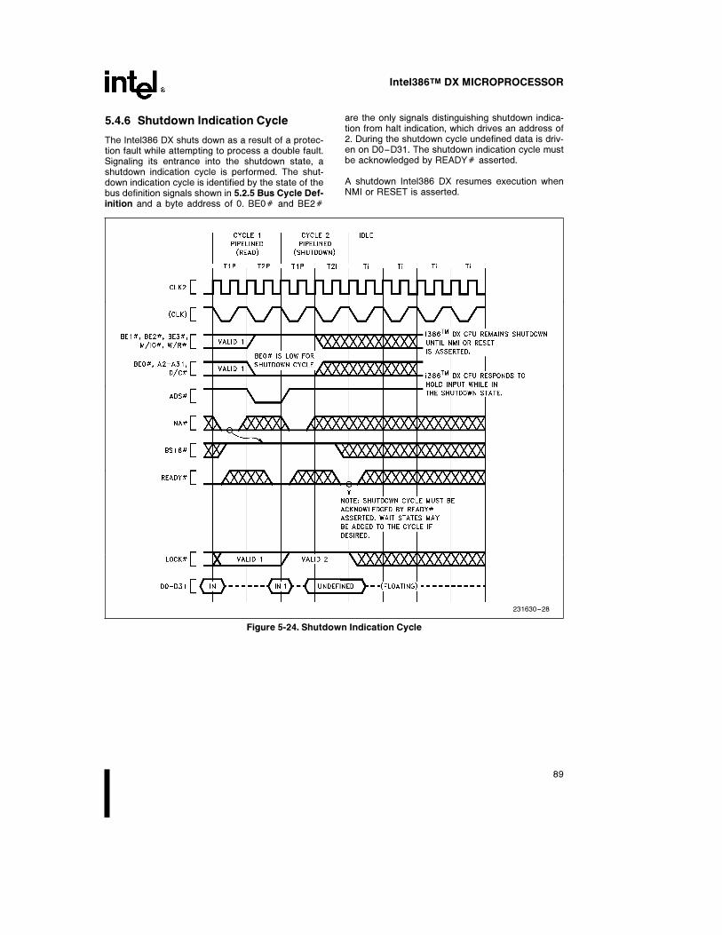
Intel386TM DX MICROPROCESSOR
5.4.6 Shutdown Indication Cycle
The Intel386 DX shuts down as a result of a protec-tion fault while attempting to process a double fault.Signaling its entrance into the shutdown state, ashutdown indication cycle is performed. The shut-down indication cycle is identified by the state of thebus definition signals shown in 5.2.5 Bus Cycle Def-inition and a byte address of 0. BE0Ý and BE2Ý
are the only signals distinguishing shutdown indica-tion from halt indication, which drives an address of2. During the shutdown cycle undefined data is driv-en on D0–D31. The shutdown indication cycle mustbe acknowledged by READYÝ asserted.
A shutdown Intel386 DX resumes execution whenNMI or RESET is asserted.
231630–28
Figure 5-24. Shutdown Indication Cycle
89
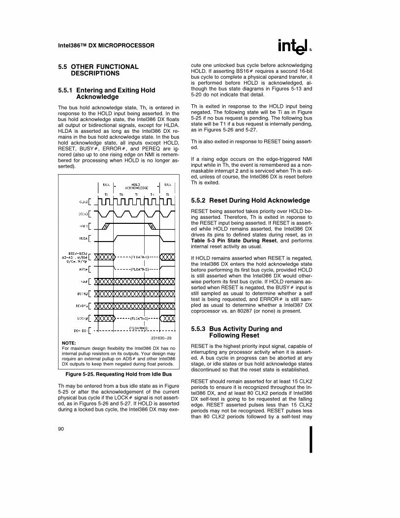
Intel386TM DX MICROPROCESSOR
5.5 OTHER FUNCTIONALDESCRIPTIONS
5.5.1 Entering and Exiting HoldAcknowledge
The bus hold acknowledge state, Th, is entered inresponse to the HOLD input being asserted. In thebus hold acknowledge state, the Intel386 DX floatsall output or bidirectional signals, except for HLDA.HLDA is asserted as long as the Intel386 DX re-mains in the bus hold acknowledge state. In the bushold acknowledge state, all inputs except HOLD,RESET, BUSYÝ, ERRORÝ, and PEREQ are ig-nored (also up to one rising edge on NMI is remem-bered for processing when HOLD is no longer as-serted).
231630–29
NOTE:For maximum design flexibility the Intel386 DX has nointernal pullup resistors on its outputs. Your design mayrequire an external pullup on ADSÝ and other Intel386DX outputs to keep them negated during float periods.
Figure 5-25. Requesting Hold from Idle Bus
Th may be entered from a bus idle state as in Figure5-25 or after the acknowledgement of the currentphysical bus cycle if the LOCKÝ signal is not assert-ed, as in Figures 5-26 and 5-27. If HOLD is assertedduring a locked bus cycle, the Intel386 DX may exe-
cute one unlocked bus cycle before acknowledgingHOLD. If asserting BS16Ý requires a second 16-bitbus cycle to complete a physical operand transfer, itis performed before HOLD is acknowledged, al-though the bus state diagrams in Figures 5-13 and5-20 do not indicate that detail.
Th is exited in response to the HOLD input beingnegated. The following state will be Ti as in Figure5-25 if no bus request is pending. The following busstate will be T1 if a bus request is internally pending,as in Figures 5-26 and 5-27.
Th is also exited in response to RESET being assert-ed.
If a rising edge occurs on the edge-triggered NMIinput while in Th, the event is remembered as a non-maskable interrupt 2 and is serviced when Th is exit-ed, unless of course, the Intel386 DX is reset beforeTh is exited.
5.5.2 Reset During Hold Acknowledge
RESET being asserted takes priority over HOLD be-ing asserted. Therefore, Th is exited in reponse tothe RESET input being asserted. If RESET is assert-ed while HOLD remains asserted, the Intel386 DXdrives its pins to defined states during reset, as inTable 5-3 Pin State During Reset, and performsinternal reset activity as usual.
If HOLD remains asserted when RESET is negated,the Intel386 DX enters the hold acknowledge statebefore performing its first bus cycle, provided HOLDis still asserted when the Intel386 DX would other-wise perform its first bus cycle. If HOLD remains as-serted when RESET is negated, the BUSYÝ input isstill sampled as usual to determine whether a selftest is being requested, and ERRORÝ is still sam-pled as usual to determine whether a Intel387 DXcoprocessor vs. an 80287 (or none) is present.
5.5.3 Bus Activity During andFollowing Reset
RESET is the highest priority input signal, capable ofinterrupting any processor activity when it is assert-ed. A bus cycle in progress can be aborted at anystage, or idle states or bus hold acknowledge statesdiscontinued so that the reset state is established.
RESET should remain asserted for at least 15 CLK2periods to ensure it is recognized throughout the In-tel386 DX, and at least 80 CLK2 periods if Intel386DX self-test is going to be requested at the fallingedge. RESET asserted pulses less than 15 CLK2periods may not be recognized. RESET pulses lessthan 80 CLK2 periods followed by a self-test may
90
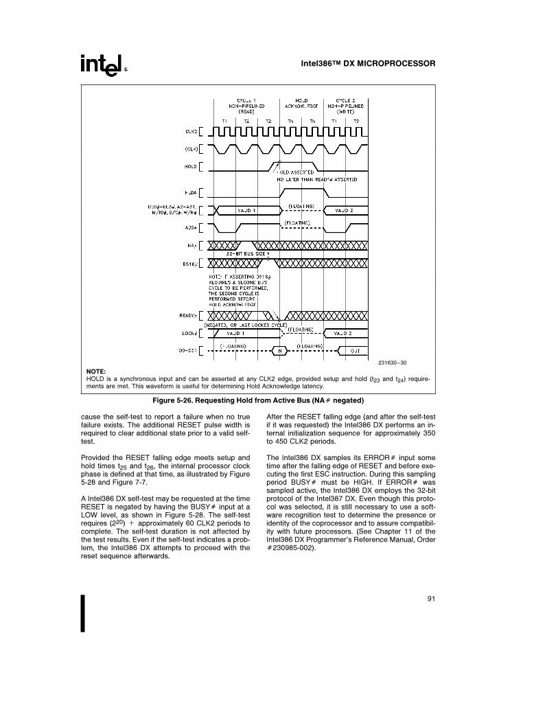
Intel386TM DX MICROPROCESSOR
231630–30
NOTE:HOLD is a synchronous input and can be asserted at any CLK2 edge, provided setup and hold (t23 and t24) require-ments are met. This waveform is useful for determining Hold Acknowledge latency.
Figure 5-26. Requesting Hold from Active Bus (NAÝ negated)
cause the self-test to report a failure when no truefailure exists. The additional RESET pulse width isrequired to clear additional state prior to a valid self-test.
Provided the RESET falling edge meets setup andhold times t25 and t26, the internal processor clockphase is defined at that time, as illustrated by Figure5-28 and Figure 7-7.
A Intel386 DX self-test may be requested at the timeRESET is negated by having the BUSYÝ input at aLOW level, as shown in Figure 5-28. The self-testrequires (220) a approximately 60 CLK2 periods tocomplete. The self-test duration is not affected bythe test results. Even if the self-test indicates a prob-lem, the Intel386 DX attempts to proceed with thereset sequence afterwards.
After the RESET falling edge (and after the self-testif it was requested) the Intel386 DX performs an in-ternal initialization sequence for approximately 350to 450 CLK2 periods.
The Intel386 DX samples its ERRORÝ input sometime after the falling edge of RESET and before exe-cuting the first ESC instruction. During this samplingperiod BUSYÝ must be HIGH. If ERRORÝ wassampled active, the Intel386 DX employs the 32-bitprotocol of the Intel387 DX. Even though this proto-col was selected, it is still necessary to use a soft-ware recognition test to determine the presence oridentity of the coprocessor and to assure compatibil-ity with future processors. (See Chapter 11 of theIntel386 DX Programmer’s Reference Manual, OrderÝ230985-002).
91

Intel386TM DX MICROPROCESSOR
231630–31
NOTE:HOLD is a synchronous input and can be asserted at any CLK2 edge, provided setup and hold (t23 and t24) require-ments are met. This waveform is useful for determining Hold Acknowledge latency.
Figure 5-27. Requesting Hold from Active Bus (NAÝ asserted)
5.6 SELF-TEST SIGNATURE
Upon completion of self-test, (if self-test was re-quested by holding BUSYÝ LOW at least eightCLK2 periods before and after the falling edge ofRESET), the EAX register will contain a signature of00000000h indicating the Intel386 DX passed itsself-test of microcode and major PLA contents withno problems detected. The passing signature inEAX, 00000000h, applies to all Intel386 DX revisionlevels. Any non-zero signature indicates the Intel386DX unit is faulty.
5.7 COMPONENT AND REVISIONIDENTIFIERS
To assist Intel386 DX users, the Intel386 DX afterreset holds a component identifier and a revision
identifier in its DX register. The upper 8 bits of DXhold 03h as identification of the Intel386 DX compo-nent. The lower 8 bits of DX hold an 8-bit unsignedbinary number related to the component revisionlevel. The revision identifier begins chronologicallywith a value zero and is subject to change (typicallyit will be incremented) with component steppings in-tended to have certain improvements or distinctionsfrom previous steppings.
These features are intended to assist Intel386 DXusers to a practical extent. However, the revisionidentifier value is not guaranteed to change with ev-ery stepping revision, or to follow a completely uni-form numerical sequence, depending on the type orintention of revision, or manufacturing materials re-quired to be changed. Intel has sole discretion overthese characteristics of the component.
92

Intel386TM DX MICROPROCESSOR
231630–32
NOTES:1. BUSYÝ should be held stable for 8 CLK2 periods before and after the CLK2 period in which RESET falling edgeoccurs.2. If self-test is requested, the Intel386 DX outputs remain in their reset state as shown here and in Table 5-3.
Figure 5-28. Bus Activity from Reset Until First Code Fetch
Table 5-10. Component and Revision Identifier History
Intel386TM DXComponent Revision
Intel386 DXComponent Revision
SteppingIdentifier Identifier
SteppingIdentifier Identifier
Name Name
B0 03 03 D0 03 05
B1 03 03 D1 03 08
93
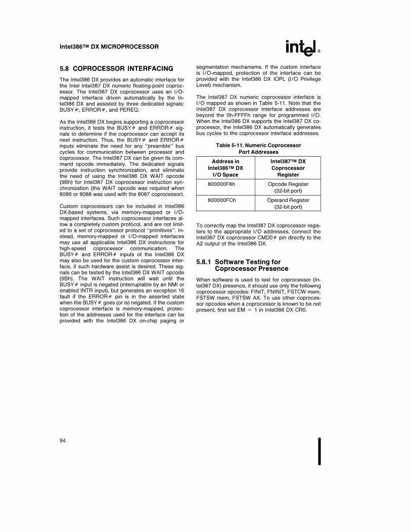
Intel386TM DX MICROPROCESSOR
5.8 COPROCESSOR INTERFACING
The Intel386 DX provides an automatic interface forthe Intel Intel387 DX numeric floating-point coproc-essor. The Intel387 DX coprocessor uses an I/O-mapped interface driven automatically by the In-tel386 DX and assisted by three dedicated signals:BUSYÝ, ERRORÝ, and PEREQ.
As the Intel386 DX begins supporting a coprocessorinstruction, it tests the BUSYÝ and ERRORÝ sig-nals to determine if the coprocessor can accept itsnext instruction. Thus, the BUSYÝ and ERRORÝinputs eliminate the need for any ‘‘preamble’’ buscycles for communication between processor andcoprocessor. The Intel387 DX can be given its com-mand opcode immediately. The dedicated signalsprovide instruction synchronization, and eliminatethe need of using the Intel386 DX WAIT opcode(9Bh) for Intel387 DX coprocessor instruction syn-chronization (the WAIT opcode was required when8086 or 8088 was used with the 8087 coprocessor).
Custom coprocessors can be included in Intel386DX-based systems, via memory-mapped or I/O-mapped interfaces. Such coprocessor interfaces al-low a completely custom protocol, and are not limit-ed to a set of coprocessor protocol ‘‘primitives’’. In-stead, memory-mapped or I/O-mapped interfacesmay use all applicable Intel386 DX instructions forhigh-speed coprocessor communication. TheBUSYÝ and ERRORÝ inputs of the Intel386 DXmay also be used for the custom coprocessor inter-face, if such hardware assist is desired. These sig-nals can be tested by the Intel386 DX WAIT opcode(9Bh). The WAIT instruction will wait until theBUSYÝ input is negated (interruptable by an NMI orenabled INTR input), but generates an exception 16fault if the ERRORÝ pin is in the asserted statewhen the BUSYÝ goes (or is) negated. If the customcoprocessor interface is memory-mapped, protec-tion of the addresses used for the interface can beprovided with the Intel386 DX on-chip paging or
segmentation mechanisms. If the custom interfaceis I/O-mapped, protection of the interface can beprovided with the Intel386 DX IOPL (I/O PrivilegeLevel) mechanism.
The Intel387 DX numeric coprocessor interface isI/O mapped as shown in Table 5-11. Note that theIntel387 DX coprocessor interface addresses arebeyond the 0h-FFFFh range for programmed I/O.When the Intel386 DX supports the Intel387 DX co-processor, the Intel386 DX automatically generatesbus cycles to the coprocessor interface addresses.
Table 5-11. Numeric Coprocessor
Port Addresses
Address in Intel387TM DX
Intel386TM DX Coprocessor
I/O Space Register
800000F8h Opcode Register
(32-bit port)
800000FCh Operand Register
(32-bit port)
To correctly map the Intel387 DX coprocessor regis-ters to the appropriate I/O addresses, connect theIntel387 DX coprocessor CMD0Ý pin directly to theA2 output of the Intel386 DX.
5.8.1 Software Testing forCoprocessor Presence
When software is used to test for coprocessor (In-tel387 DX) presence, it should use only the followingcoprocessor opcodes: FINIT, FNINIT, FSTCW mem,FSTSW mem, FSTSW AX. To use other coproces-sor opcodes when a coprocessor is known to be notpresent, first set EM e 1 in Intel386 DX CR0.
94

Intel386TM DX MICROPROCESSOR
6. INSTRUCTION SET
This section describes the Intel386 DX instructionset. A table lists all instructions along with instructionencoding diagrams and clock counts. Further detailsof the instruction encoding are then provided in thefollowing sections, which completely describe theencoding structure and the definition of all fields oc-curring within Intel386 DX instructions.
6.1 Intel386TM DX INSTRUCTIONENCODING AND CLOCK COUNTSUMMARY
To calculate elapsed time for an instruction, multiplythe instruction clock count, as listed in Table 6-1below, by the processor clock period (e.g. 50 ns fora 20 MHz Intel386 DX, 40 ns for a 25 MHz Intel386DX, and 30 ns for a 33 MHz Intel386 DX).
For more detailed information on the encodings ofinstructions refer to section 6.2 Instruction Encod-ings. Section 6.2 explains the general structure ofinstruction encodings, and defines exactly the en-codings of all fields contained within the instruction.
Instruction Clock Count Assumptions
1. The instruction has been prefetched, decoded,and is ready for execution.
2. Bus cycles do not require wait states.
3. There are no local bus HOLD requests delayingprocessor access to the bus.
4. No exceptions are detected during instruction ex-ecution.
5. If an effective address is calculated, it does notuse two general register components. One regis-ter, scaling and displacement can be used withinthe clock counts shown. However, if the effectiveaddress calculation uses two general registercomponents, add 1 clock to the clock countshown.
Instruction Clock Count Notation
1. If two clock counts are given, the smaller refers toa register operand and the larger refers to a mem-ory operand.
2. n e number of times repeated.
3. m e number of components in the next instruc-tion executed, where the entire displacement (ifany) counts as one component, the entire imme-diate data (if any) counts as one component, andeach of the other bytes of the instruction and pre-fix(es) each count as one component.
Wait States
Add 1 clock per wait state to instruction executionfor each data access.
95
Intel386TM DX MICROPROCESSOR
Table 6-1. Intel386TM DX Instruction Set Clock Count Summary
CLOCK COUNT NOTES
Real RealINSTRUCTION FORMAT Address Protected Address Protected
Mode or Virtual Mode or VirtualVirtual Address Virtual Address8086 Mode 8086 ModeMode Mode
GENERAL DATA TRANSFER
MOV e Move:
Register to Register/Memory 1 0 0 0 1 0 0 w mod reg r/m 2/2 2/2 b h
Register/Memory to Register 1 0 0 0 1 0 1 w mod reg r/m 2/4 2/4 b h
Immediate to Register/Memory 1 1 0 0 0 1 1 w mod 0 0 0 r/m immediate data 2/2 2/2 b h
Immediate to Register (short form) 1 0 1 1 w reg immediate data 2 2
Memory to Accumulator (short form) 1 0 1 0 0 0 0 w full displacement 4 4 b h
Accumulator to Memory (short form) 1 0 1 0 0 0 1 w full displacement 2 2 b h
Register Memory to Segment Register 1 0 0 0 1 1 1 0 mod sreg3 r/m 2/5 18/19 b h, i, j
Segment Register to Register/Memory 1 0 0 0 1 1 0 0 mod sreg3 r/m 2/2 2/2 b h
MOVSX e Move With Sign Extension
Register From Register/Memory 0 0 0 0 1 1 1 1 1 0 1 1 1 1 1 w mod reg r/m 3/6 3/6 b h
MOVZX e Move With Zero Extension
Register From Register/Memory 0 0 0 0 1 1 1 1 1 0 1 1 0 1 1 w mod reg r/m 3/6 3/6 b h
PUSH e Push:
Register/Memory 1 1 1 1 1 1 1 1 mod 1 1 0 r/m 5 5 b h
Register (short form) 0 1 0 1 0 reg 2 2 b h
Segment Register (ES, CS, SS or DS)0 0 0 sreg2 1 1 0 2 2 b h
Segment Register (FS or GS)0 0 0 0 1 1 1 1 1 0 sreg3 0 0 0 2 2 b h
Immediate 0 1 1 0 1 0 s 0 immediate data 2 2 b h
PUSHA e Push All 0 1 1 0 0 0 0 0 18 18 b h
POP e Pop
Register/Memory 1 0 0 0 1 1 1 1 mod 0 0 0 r/m 5 5 b h
Register (short form) 0 1 0 1 1 reg 4 4 b h
Segment Register (ES, SS or DS)0 0 0 sreg 2 1 1 1 7 21 b h, i, j
Segment Register (FS or GS)0 0 0 0 1 1 1 1 1 0 sreg 3 0 0 1 7 21 b h, i, j
POPA e Pop All 0 1 1 0 0 0 0 1 24 24 b h
XCHG e Exchange
Register/Memory With Register 1 0 0 0 0 1 1 w mod reg r/m 3/5 3/5 b, f f, h
Register With Accumulator (short form) 1 0 0 1 0 reg
8086 Mode
Clk CountVirtual
3 3
IN e Input from:
Fixed Port 1 1 1 0 0 1 0 w port number ²26 12 6*/26** m
Variable Port 1 1 1 0 1 1 0 w ²27 13 7*/27** m
OUT e Output to:
Fixed Port 1 1 1 0 0 1 1 w port number ²24 10 4*/24** m
Variable Port 1 1 1 0 1 1 1 w ²25 11 5*/25** m
LEA e Load EA to Register 1 0 0 0 1 1 0 1 mod reg r/m 2 2
* If CPL s IOPL ** If CPL l IOPL
96

Intel386TM DX MICROPROCESSOR
Table 6-1. Intel386TM DX Instruction Set Clock Count Summary (Continued)
CLOCK COUNT NOTES
Real RealINSTRUCTION FORMAT Address Protected Address Protected
Mode or Virtual Mode or VirtualVirtual Address Virtual Address8086 Mode 8086 ModeMode Mode
SEGMENT CONTROL
LDS e Load Pointer to DS 1 1 0 0 0 1 0 1 mod reg r/m 7 22 b h, i, j
LES e Load Pointer to ES 1 1 0 0 0 1 0 0 mod reg r/m 7 22 b h, i, j
LFS e Load Pointer to FS 0 0 0 0 1 1 1 1 1 0 1 1 0 1 0 0 mod reg r/m 7 25 b h, i, j
LGS e Load Pointer to GS 0 0 0 0 1 1 1 1 1 0 1 1 0 1 0 1 mod reg r/m 7 25 b h, i, j
LSS e Load Pointer to SS 0 0 0 0 1 1 1 1 1 0 1 1 0 0 1 0 mod reg r/m 7 22 b h, i, j
FLAG CONTROL
CLC e Clear Carry Flag 1 1 1 1 1 0 0 0 2 2
CLD e Clear Direction Flag 1 1 1 1 1 1 0 0 2 2
CLI e Clear Interrupt Enable Flag 1 1 1 1 1 0 1 0 8 8 m
CLTS e Clear Task Switched Flag 0 0 0 0 1 1 1 1 0 0 0 0 0 1 1 0 6 6 c l
CMC e Complement Carry Flag 1 1 1 1 0 1 0 1 2 2
LAHF e Load AH into Flag 1 0 0 1 1 1 1 1 2 2
POPF e Pop Flags 1 0 0 1 1 1 0 1 5 5 b h, n
PUSHF e Push Flags 1 0 0 1 1 1 0 0 4 4 b h
SAHF e Store AH into Flags 1 0 0 1 1 1 1 0 3 3
STC e Set Carry Flag 1 1 1 1 1 0 0 1 2 2
STD e Set Direction Flag 1 1 1 1 1 1 0 1 2 2
STI e Set Interrupt Enable Flag 1 1 1 1 1 0 1 1 8 8 m
ARITHMETIC
ADD e Add
Register to Register 0 0 0 0 0 0 d w mod reg r/m 2 2
Register to Memory 0 0 0 0 0 0 0 w mod reg r/m 7 7 b h
Memory to Register 0 0 0 0 0 0 1 w mod reg r/m 6 6 b h
Immediate to Register/Memory 1 0 0 0 0 0 s w mod 0 0 0 r/m immediate data 2/7 2/7 b h
Immediate to Accumulator (short form) 0 0 0 0 0 1 0 w immediate data 2 2
ADC e Add With Carry
Register to Register 0 0 0 1 0 0 d w mod reg r/m 2 2
Register to Memory 0 0 0 1 0 0 0 w mod reg r/m 7 7 b h
Memory to Register 0 0 0 1 0 0 1 w mod reg r/m 6 6 b h
Immediate to Register/Memory 1 0 0 0 0 0 s w mod 0 1 0 r/m immediate data 2/7 2/7 b h
Immediate to Accumulator (short form) 0 0 0 1 0 1 0 w immediate data 2 2
INC e Increment
Register/Memory 1 1 1 1 1 1 1 w mod 0 0 0 r/m 2/6 2/6 b h
Register (short form) 0 1 0 0 0 reg 2 2
SUB e Subtract
Register from Register 0 0 1 0 1 0 d w mod reg r/m 2 2
97

Intel386TM DX MICROPROCESSOR
Table 6-1. Intel386TM DX Instruction Set Clock Count Summary (Continued)
CLOCK COUNT NOTES
Real RealINSTRUCTION FORMAT Address Protected Address Protected
Mode or Virtual Mode or VirtualVirtual Address Virtual Address8086 Mode 8086 ModeMode Mode
ARITHMETIC (Continued)
Register from Memory 0 0 1 0 1 0 0 w mod reg r/m 7 7 b h
Memory from Register 0 0 1 0 1 0 1 w mod reg r/m 6 6 b h
Immediate from Register/Memory 1 0 0 0 0 0 s w mod 1 0 1 r/m immediate data 2/7 2/7 b h
Immediate from Accumulator (short form) 0 0 1 0 1 1 0 w immediate data 2 2
SBB e Subtract with Borrow
Register from Register 0 0 0 1 1 0 d w mod reg r/m 2 2
Register from Memory 0 0 0 1 1 0 0 w mod reg r/m 7 7 b h
Memory from Register 0 0 0 1 1 0 1 w mod reg r/m 6 6 b h
Immediate from Register/Memory 1 0 0 0 0 0 s w mod 0 1 1 r/m immediate data 2/7 2/7 b h
Immediate from Accumulator (short form) 0 0 0 1 1 1 0 w immediate data 2 2
DEC e Decrement
Register/Memory 1 1 1 1 1 1 1 w reg 0 0 1 r/m 2/6 2/6 b h
Register (short form) 0 1 0 0 1 reg 2 2
CMP e Compare
Register with Register 0 0 1 1 1 0 d w mod reg r/m 2 2
Memory with Register 0 0 1 1 1 0 0 w mod reg r/m 5 5 b h
Register with Memory 0 0 1 1 1 0 1 w mod reg r/m 6 6 b h
Immediate with Register/Memory 1 0 0 0 0 0 s w mod 1 1 1 r/m immediate data 2/5 2/5 b h
Immediate with Accumulator (short form) 0 0 1 1 1 1 0 w immediate data 2 2
NEG e Change Sign 1 1 1 1 0 1 1 w mod 0 1 1 r/m 2/6 2/6 b h
AAA e ASCII Adjust for Add 0 0 1 1 0 1 1 1 4 4
AAS e ASCII Adjust for Subtract 0 0 1 1 1 1 1 1 4 4
DAA e Decimal Adjust for Add 0 0 1 0 0 1 1 1 4 4
DAS e Decimal Adjust for Subtract 0 0 1 0 1 1 1 1 4 4
MUL e Multiply (unsigned)
Accumulator with Register/Memory 1 1 1 1 0 1 1 w mod 1 0 0 r/m
Multiplier-Byte 12–17/15-20 12–17/15–20 b, d d, h
-Word 12–25/15-28 12–25/15–28 b, d d, h
-Doubleword 12–41/15-44 12–41/15–44 b, d d, h
IMUL e Integer Multiply (signed)
Accumulator with Register/Memory 1 1 1 1 0 1 1 w mod 1 0 1 r/m
Multiplier-Byte 12–17/15-20 12–17/15–20 b, d d, h
-Word 12–25/15-28 12–25/15–28 b, d d, h
-Doubleword 12–41/15-44 12–41/15–44 b, d d, h
Register with Register/Memory 0 0 0 0 1 1 1 1 1 0 1 0 1 1 1 1 mod reg r/m
Multiplier-Byte 12–17/15-20 12–17/15–20 b, d d, h
-Word 12–25/15-28 12–25/15–28 b, d d, h
-Doubleword 12–41/15-44 12–41/15–44 b, d d, h
Register/Memory with Immediate to Register 0 1 1 0 1 0 s 1 mod reg r/m immediate data
-Word 13–26/14-27 13–26/14–27 b, d d, h
-Doubleword 13–42/14-43 13–42/14–43 b, d d, h
98

Intel386TM DX MICROPROCESSOR
Table 6-1. Intel386TM DX Instruction Set Clock Count Summary (Continued)
CLOCK COUNT NOTES
Real RealINSTRUCTION FORMAT Address Protected Address Protected
Mode or Virtual Mode or VirtualVirtual Address Virtual Address8086 Mode 8086 ModeMode Mode
ARITHMETIC (Continued)
DIV e Divide (Unsigned)
Accumulator by Register/Memory 1 1 1 1 0 1 1 w mod 1 1 0 r/m
DivisorÐByte 14/17 14/17 b,e e,h
ÐWord 22/25 22/25 b,e e,h
ÐDoubleword 38/41 38/41 b,e e,h
IDIV e Integer Divide (Signed)
Accumulator By Register/Memory 1 1 1 1 0 1 1 w mod 1 1 1 r/m
DivisorÐByte 19/22 19/22 b,e e,h
ÐWord 27/30 27/30 b,e e,h
ÐDoubleword 43/46 43/46 b,e e,h
AAD e ASCII Adjust for Divide 1 1 0 1 0 1 0 1 0 0 0 0 1 0 1 0 19 19
AAM e ASCII Adjust for Multiply 1 1 0 1 0 1 0 0 0 0 0 0 1 0 1 0 17 17
CBW e Convert Byte to Word 1 0 0 1 1 0 0 0 3 3
CWD e Convert Word to Double Word 1 0 0 1 1 0 0 1 2 2
LOGIC
Shift Rotate Instructions
Not Through Carry (ROL, ROR, SAL, SAR, SHL, and SHR)
Register/Memory by 1 1 1 0 1 0 0 0 w mod TTT r/m 3/7 3/7 b h
Register/Memory by CL 1 1 0 1 0 0 1 w mod TTT r/m 3/7 3/7 b h
Register/Memory by Immediate Count 1 1 0 0 0 0 0 w mod TTT r/m immed 8-bit data 3/7 3/7 b h
Through Carry (RCL and RCR)
Register/Memory by 1 1 1 0 1 0 0 0 w mod TTT r/m 9/10 9/10 b h
Register/Memory by CL 1 1 0 1 0 0 1 w mod TTT r/m 9/10 9/10 b h
Register/Memory by Immediate Count 1 1 0 0 0 0 0 w mod TTT r/m immed 8-bit data 9/10 9/10 b h
T T T Instruction
0 0 0 ROL
0 0 1 ROR
0 1 0 RCL
0 1 1 RCR
1 0 0 SHL/SAL
1 0 1 SHR
1 1 1 SAR
SHLD e Shift Left Double
Register/Memory by Immediate 0 0 0 0 1 1 1 1 1 0 1 0 0 1 0 0 mod reg r/m immed 8-bit data 3/7 3/7
Register/Memory by CL 0 0 0 0 1 1 1 1 1 0 1 0 0 1 0 1 mod reg r/m 3/7 3/7
SHRD e Shift Right Double
Register/Memory by Immediate 0 0 0 0 1 1 1 1 1 0 1 0 1 1 0 0 mod reg r/m immed 8-bit data 3/7 3/7
Register/Memory by CL 0 0 0 0 1 1 1 1 1 0 1 0 1 1 0 1 mod reg r/m 3/7 3/7
AND e And
Register to Register 0 0 1 0 0 0 d w mod reg r/m 2 2
99
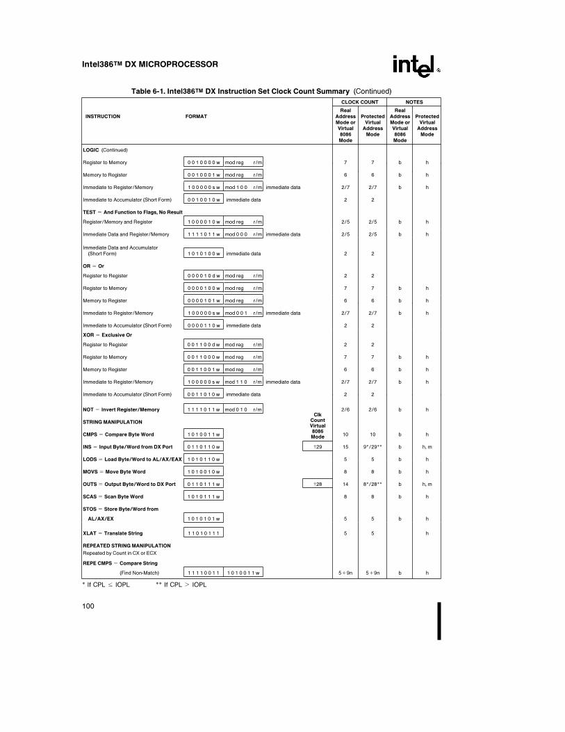
Intel386TM DX MICROPROCESSOR
Table 6-1. Intel386TM DX Instruction Set Clock Count Summary (Continued)
CLOCK COUNT NOTES
Real RealINSTRUCTION FORMAT Address Protected Address Protected
Mode or Virtual Mode or VirtualVirtual Address Virtual Address8086 Mode 8086 ModeMode Mode
LOGIC (Continued)
Register to Memory 0 0 1 0 0 0 0 w mod reg r/m 7 7 b h
Memory to Register 0 0 1 0 0 0 1 w mod reg r/m 6 6 b h
Immediate to Register/Memory 1 0 0 0 0 0 s w mod 1 0 0 r/m immediate data 2/7 2/7 b h
Immediate to Accumulator (Short Form) 0 0 1 0 0 1 0 w immediate data 2 2
TEST e And Function to Flags, No Result
Register/Memory and Register 1 0 0 0 0 1 0 w mod reg r/m 2/5 2/5 b h
Immediate Data and Register/Memory 1 1 1 1 0 1 1 w mod 0 0 0 r/m immediate data 2/5 2/5 b h
Immediate Data and Accumulator(Short Form) 1 0 1 0 1 0 0 w immediate data 2 2
OR e Or
Register to Register 0 0 0 0 1 0 d w mod reg r/m 2 2
Register to Memory 0 0 0 0 1 0 0 w mod reg r/m 7 7 b h
Memory to Register 0 0 0 0 1 0 1 w mod reg r/m 6 6 b h
Immediate to Register/Memory 1 0 0 0 0 0 s w mod 0 0 1 r/m immediate data 2/7 2/7 b h
Immediate to Accumulator (Short Form) 0 0 0 0 1 1 0 w immediate data 2 2
XOR e Exclusive Or
Register to Register 0 0 1 1 0 0 d w mod reg r/m 2 2
Register to Memory 0 0 1 1 0 0 0 w mod reg r/m 7 7 b h
Memory to Register 0 0 1 1 0 0 1 w mod reg r/m 6 6 b h
Immediate to Register/Memory 1 0 0 0 0 0 s w mod 1 1 0 r/m immediate data 2/7 2/7 b h
Immediate to Accumulator (Short Form) 0 0 1 1 0 1 0 w immediate data 2 2
NOT e Invert Register/Memory 1 1 1 1 0 1 1 w mod 0 1 0 r/m 2/6 2/6 b h
STRING MANIPULATION
CMPS e Compare Byte Word 1 0 1 0 0 1 1 w
VirtualCount
Mode8086
Clk
10 10 b h
INS e Input Byte/Word from DX Port 0 1 1 0 1 1 0 w ²29 15 9*/29** b h, m
LODS e Load Byte/Word to AL/AX/EAX 1 0 1 0 1 1 0 w 5 5 b h
MOVS e Move Byte Word 1 0 1 0 0 1 0 w 8 8 b h
OUTS e Output Byte/Word to DX Port 0 1 1 0 1 1 1 w ²28 14 8*/28** b h, m
SCAS e Scan Byte Word 1 0 1 0 1 1 1 w 8 8 b h
STOS e Store Byte/Word from
AL/AX/EX 1 0 1 0 1 0 1 w 5 5 b h
XLAT e Translate String 1 1 0 1 0 1 1 1 5 5 h
REPEATED STRING MANIPULATION
Repeated by Count in CX or ECX
REPE CMPS e Compare String
(Find Non-Match) 1 1 1 1 0 0 1 1 1 0 1 0 0 1 1 w 5a9n 5a9n b h
* If CPL s IOPL ** If CPL l IOPL
100
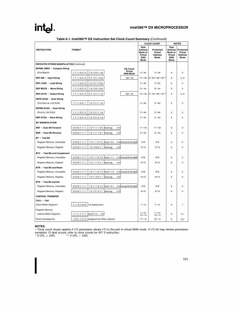
Intel386TM DX MICROPROCESSOR
Table 6-1. Intel386TM DX Instruction Set Clock Count Summary (Continued)
CLOCK COUNT NOTES
Real RealINSTRUCTION FORMAT Address Protected Address Protected
Mode or Virtual Mode or VirtualVirtual Address Virtual Address8086 Mode 8086 ModeMode Mode
REPEATED STRING MANIPULATION (Continued)
REPNE CMPS e Compare String
(Find Match) 1 1 1 1 0 0 1 0 1 0 1 0 0 1 1 w 8086 Mode
Clk CountVirtual
5a9n 5a9n b h
REP INS e Input String 1 1 1 1 0 0 1 0 0 1 1 0 1 1 0 w ²28a6n 14a6n 8a6n*/28a6n** b h, m
REP LODS e Load String 1 1 1 1 0 0 1 0 1 0 1 0 1 1 0 w 5a6n 5a6n b h
REP MOVS e Move String 1 1 1 1 0 0 1 0 1 0 1 0 0 1 0 w 8a4n 8a4n b h
REP OUTS e Output String 1 1 1 1 0 0 1 0 0 1 1 0 1 1 1 w ²26a5n 12a5n 6a5n*/26a5n** b h, m
REPE SCAS e Scan String
(Find Non-AL/AX/EAX) 1 1 1 1 0 0 1 1 1 0 1 0 1 1 1 w 5a8n 5a8n b h
REPNE SCAS e Scan String
(Find AL/AX/EAX) 1 1 1 1 0 0 1 0 1 0 1 0 1 1 1 w 5a8n 5a8n b h
REP STOS e Store String 1 1 1 1 0 0 1 0 1 0 1 0 1 0 1 w 5a5n 5a5n b h
BIT MANIPULATION
BSF e Scan Bit Forward 0 0 0 0 1 1 1 1 1 0 1 1 1 1 0 0 mod reg r/m 11a3n 11a3n b h
BSR e Scan Bit Reverse 0 0 0 0 1 1 1 1 1 0 1 1 1 1 0 1 mod reg r/m 9a3n 9a3n b h
BT e Test Bit
Register/Memory, Immediate 0 0 0 0 1 1 1 1 1 0 1 1 1 0 1 0 mod 1 0 0 r/m immed 8-bit data 3/6 3/6 b h
Register/Memory, Register 0 0 0 0 1 1 1 1 1 0 1 0 0 0 1 1 mod reg r/m 3/12 3/12 b h
BTC e Test Bit and Complement
Register/Memory, Immediate 0 0 0 0 1 1 1 1 1 0 1 1 1 0 1 0 mod 1 1 1 r/m immed 8-bit data 6/8 6/8 b h
Register/Memory, Register 0 0 0 0 1 1 1 1 1 0 1 1 1 0 1 1 mod reg r/m 6/13 6/13 b h
BTR e Test Bit and Reset
Register/Memory, Immediate 0 0 0 0 1 1 1 1 1 0 1 1 1 0 1 0 mod 1 1 0 r/m immed 8-bit data 6/8 6/8 b h
Register/Memory, Register 0 0 0 0 1 1 1 1 1 0 1 1 0 0 1 1 mod reg r/m 6/13 6/13 b h
BTS e Test Bit and Set
Register/Memory, Immediate 0 0 0 0 1 1 1 1 1 0 1 1 1 0 1 0 mod 1 0 1 r/m immed 8-bit data 6/8 6/8 b h
Register/Memory, Register 0 0 0 0 1 1 1 1 1 0 1 0 1 0 1 1 mod reg r/m 6/13 6/13 b h
CONTROL TRANSFER
CALL e Call
Direct Within Segment 1 1 1 0 1 0 0 0 full displacement 7am 7am b r
Register/Memory
Indirect Within Segment 1 1 1 1 1 1 1 1 mod 0 1 0 r/m10am7am/
10am7am/
b h, r
Direct Intersegment 1 0 0 1 1 0 1 0 unsigned full offset, selector 17am 34am b j,k,r
NOTES:² Clock count shown applies if I/O permission allows I/O to the port in virtual 8086 mode. If I/O bit map denies permissionexception 13 fault occurs; refer to clock counts for INT 3 instruction.* If CPL s IOPL ** If CPL l IOPL
101
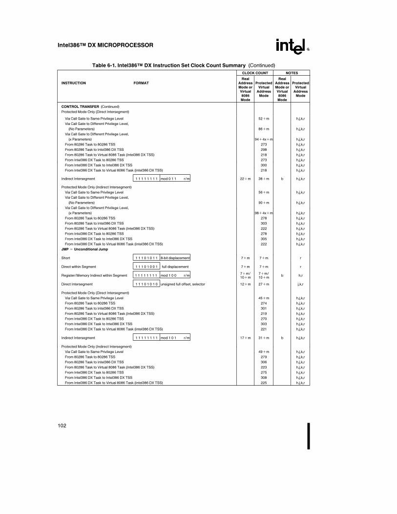
Intel386TM DX MICROPROCESSOR
Table 6-1. Intel386TM DX Instruction Set Clock Count Summary (Continued)
CLOCK COUNT NOTES
Real RealINSTRUCTION FORMAT Address Protected Address Protected
Mode or Virtual Mode or VirtualVirtual Address Virtual Address8086 Mode 8086 ModeMode Mode
CONTROL TRANSFER (Continued)
Protected Mode Only (Direct Intersegment)
Via Call Gate to Same Privilege Level 52am h,j,k,r
Via Call Gate to Different Privilege Level,
(No Parameters) 86am h,j,k,r
Via Call Gate to Different Privilege Level,
(x Parameters) 94a4xam h,j,k,r
From 80286 Task to 80286 TSS 273 h,j,k,r
From 80286 Task to Intel386 DX TSS 298 h,j,k,r
From 80286 Task to Virtual 8086 Task (Intel386 DX TSS) 218 h,j,k,r
From Intel386 DX Task to 80286 TSS 273 h,j,k,r
From Intel386 DX Task to Intel386 DX TSS 300 h,j,k,r
From Intel386 DX Task to Virtual 8086 Task (Intel386 DX TSS) 218 h,j,k,r
Indirect Intersegment 1 1 1 1 1 1 1 1 mod 0 1 1 r/m 22am 38am b h,j,k,r
Protected Mode Only (Indirect Intersegment)
Via Call Gate to Same Privilege Level 56am h,j,k,r
Via Call Gate to Different Privilege Level,
(No Parameters) 90am h,j,k,r
Via Call Gate to Different Privilege Level,
(x Parameters) 98a4xam h,j,k,r
From 80286 Task to 80286 TSS 278 h,j,k,r
From 80286 Task to Intel386 DX TSS 303 h,j,k,r
From 80286 Task to Virtual 8086 Task (Intel386 DX TSS) 222 h,j,k,r
From Intel386 DX Task to 80286 TSS 278 h,j,k,r
From Intel386 DX Task to Intel386 DX TSS 305 h,j,k,r
From Intel386 DX Task to Virtual 8086 Task (Intel386 DX TSS) 222 h,j,k,r
JMP e Unconditional Jump
Short 1 1 1 0 1 0 1 1 8-bit displacement 7am 7am r
Direct within Segment 1 1 1 0 1 0 0 1 full displacement 7am 7am r
Register/Memory Indirect within Segment 1 1 1 1 1 1 1 1 mod 1 0 0 r/m10am7am/
10am7am/
b h,r
Direct Intersegment 1 1 1 0 1 0 1 0 unsigned full offset, selector 12am 27am j,k,r
Protected Mode Only (Direct Intersegment)
Via Call Gate to Same Privilege Level 45am h,j,k,r
From 80286 Task to 80286 TSS 274 h,j,k,r
From 80286 Task to Intel386 DX TSS 301 h,j,k,r
From 80286 Task to Virtual 8086 Task (Intel386 DX TSS) 219 h,j,k,r
From Intel386 DX Task to 80286 TSS 270 h,j,k,r
From Intel386 DX Task to Intel386 DX TSS 303 h,j,k,r
From Intel386 DX Task to Virtual 8086 Task (Intel386 DX TSS) 221 h,j,k,r
Indirect Intersegment 1 1 1 1 1 1 1 1 mod 1 0 1 r/m 17am 31am b h,j,k,r
Protected Mode Only (Indirect Intersegment)
Via Call Gate to Same Privilege Level 49am h,j,k,r
From 80286 Task to 80286 TSS 279 h,j,k,r
From 80286 Task to Intel386 DX TSS 306 h,j,k,r
From 80286 Task to Virtual 8086 Task (Intel386 DX TSS) 223 h,j,k,r
From Intel386 DX Task to 80286 TSS 275 h,j,k,r
From Intel386 DX Task to Intel386 DX TSS 308 h,j,k,r
From Intel386 DX Task to Virtual 8086 Task (Intel386 DX TSS) 225 h,j,k,r
102
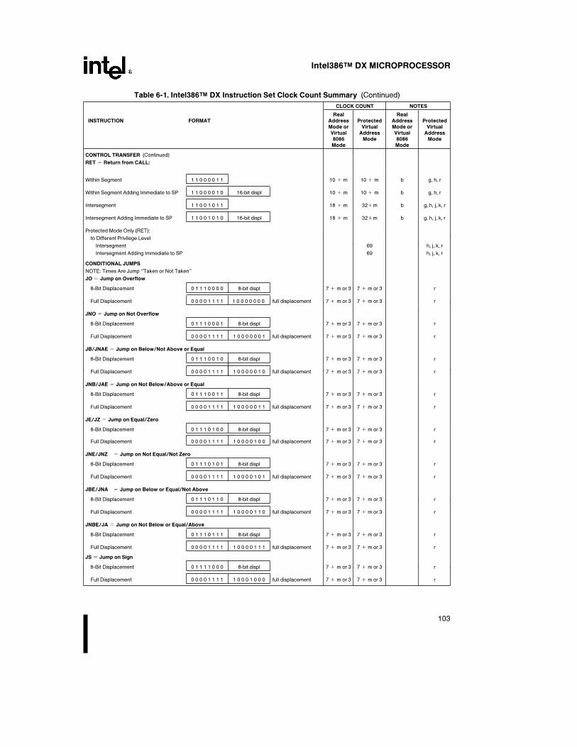
Intel386TM DX MICROPROCESSOR
Table 6-1. Intel386TM DX Instruction Set Clock Count Summary (Continued)
CLOCK COUNT NOTES
Real RealINSTRUCTION FORMAT Address Protected Address Protected
Mode or Virtual Mode or VirtualVirtual Address Virtual Address8086 Mode 8086 ModeMode Mode
CONTROL TRANSFER (Continued)
RET e Return from CALL:
Within Segment 1 1 0 0 0 0 1 1 10 a m 10 a m b g, h, r
Within Segment Adding Immediate to SP 1 1 0 0 0 0 1 0 16-bit displ 10 a m 10 a m b g, h, r
Intersegment 1 1 0 0 1 0 1 1 18 a m 32am b g, h, j, k, r
Intersegment Adding Immediate to SP 1 1 0 0 1 0 1 0 16-bit displ 18 a m 32am b g, h, j, k, r
Protected Mode Only (RET):
to Different Privilege Level
Intersegment 69 h, j, k, r
Intersegment Adding Immediate to SP 69 h, j, k, r
CONDITIONAL JUMPS
NOTE: Times Are Jump ‘‘Taken or Not Taken’’
JO e Jump on Overflow
8-Bit Displacement 0 1 1 1 0 0 0 0 8-bit displ 7 a m or 3 7 a m or 3 r
Full Displacement 0 0 0 0 1 1 1 1 1 0 0 0 0 0 0 0 full displacement 7 a m or 3 7 a m or 3 r
JNO e Jump on Not Overflow
8-Bit Displacement 0 1 1 1 0 0 0 1 8-bit displ 7 a m or 3 7 a m or 3 r
Full Displacement 0 0 0 0 1 1 1 1 1 0 0 0 0 0 0 1 full displacement 7 a m or 3 7 a m or 3 r
JB/JNAE e Jump on Below/Not Above or Equal
8-Bit Displacement 0 1 1 1 0 0 1 0 8-bit displ 7 a m or 3 7 a m or 3 r
Full Displacement 0 0 0 0 1 1 1 1 1 0 0 0 0 0 1 0 full displacement 7 a m or 3 7 a m or 3 r
JNB/JAE e Jump on Not Below/Above or Equal
8-Bit Displacement 0 1 1 1 0 0 1 1 8-bit displ 7 a m or 3 7 a m or 3 r
Full Displacement 0 0 0 0 1 1 1 1 1 0 0 0 0 0 1 1 full displacement 7 a m or 3 7 a m or 3 r
JE/JZ e Jump on Equal/Zero
8-Bit Displacement 0 1 1 1 0 1 0 0 8-bit displ 7 a m or 3 7 a m or 3 r
Full Displacement 0 0 0 0 1 1 1 1 1 0 0 0 0 1 0 0 full displacement 7 a m or 3 7 a m or 3 r
JNE/JNZ e Jump on Not Equal/Not Zero
8-Bit Displacement 0 1 1 1 0 1 0 1 8-bit displ 7 a m or 3 7 a m or 3 r
Full Displacement 0 0 0 0 1 1 1 1 1 0 0 0 0 1 0 1 full displacement 7 a m or 3 7 a m or 3 r
JBE/JNA e Jump on Below or Equal/Not Above
8-Bit Displacement 0 1 1 1 0 1 1 0 8-bit displ 7 a m or 3 7 a m or 3 r
Full Displacement 0 0 0 0 1 1 1 1 1 0 0 0 0 1 1 0 full displacement 7 a m or 3 7 a m or 3 r
JNBE/JA e Jump on Not Below or Equal/Above
8-Bit Displacement 0 1 1 1 0 1 1 1 8-bit displ 7 a m or 3 7 a m or 3 r
Full Displacement 0 0 0 0 1 1 1 1 1 0 0 0 0 1 1 1 full displacement 7 a m or 3 7 a m or 3 r
JS e Jump on Sign
8-Bit Displacement 0 1 1 1 1 0 0 0 8-bit displ 7 a m or 3 7 a m or 3 r
Full Displacement 0 0 0 0 1 1 1 1 1 0 0 0 1 0 0 0 full displacement 7 a m or 3 7 a m or 3 r
103

Intel386TM DX MICROPROCESSOR
Table 6-1. Intel386TM DX Instruction Set Clock Count Summary (Continued)
CLOCK COUNT NOTES
Real RealINSTRUCTION FORMAT Address Protected Address Protected
Mode or Virtual Mode or VirtualVirtual Address Virtual Address8086 Mode 8086 ModeMode Mode
CONDITIONAL JUMPS (Continued)
JNS e Jump on Not Sign
8-Bit Displacement 0 1 1 1 1 0 0 1 8-bit displ 7 a m or 3 7 a m or 3 r
Full Displacement 0 0 0 0 1 1 1 1 1 0 0 0 1 0 0 1 full displacement 7 a m or 3 7 a m or 3 r
JP/JPE e Jump on Parity/Parity Even
8-Bit Displacement 0 1 1 1 1 0 1 0 8-bit displ 7 a m or 3 7 a m or 3 r
Full Displacement 0 0 0 0 1 1 1 1 1 0 0 0 1 0 1 0 full displacement 7 a m or 3 7 a m or 3 r
JNP/JPO e Jump on Not Parity/Parity Odd
8-Bit Displacement 0 1 1 1 1 0 1 1 8-bit displ 7 a m or 3 7 a m or 3 r
Full Displacement 0 0 0 0 1 1 1 1 1 0 0 0 1 0 1 1 full displacement 7 a m or 3 7 a m or 3 r
JL/JNGE e Jump on Less/Not Greater or Equal
8-Bit Displacement 0 1 1 1 1 1 0 0 8-bit displ 7 a m or 3 7 a m or 3 r
Full Displacement 0 0 0 0 1 1 1 1 1 0 0 0 1 1 0 0 full displacement 7 a m or 3 7 a m or 3 r
JNL/JGE e Jump on Not Less/Greater or Equal
8-Bit Displacement 0 1 1 1 1 1 0 1 8-bit displ 7 a m or 3 7 a m or 3 r
Full Displacement 0 0 0 0 1 1 1 1 1 0 0 0 1 1 0 1 full displacement 7 a m or 3 7 a m or 3 r
JLE/JNG e Jump on Less or Equal/Not Greater
8-Bit Displacement 0 1 1 1 1 1 1 0 8-bit displ 7 a m or 3 7 a m or 3 r
Full Displacement 0 0 0 0 1 1 1 1 1 0 0 0 1 1 1 0 full displacement 7 a m or 3 7 a m or 3 r
JNLE/JG e Jump on Not Less or Equal/Greater
8-Bit Displacement 0 1 1 1 1 1 1 1 8-bit displ 7 a m or 3 7 a m or 3 r
Full Displacement 0 0 0 0 1 1 1 1 1 0 0 0 1 1 1 1 full displacement 7 a m or 3 7 a m or 3 r
JCXZ e Jump on CX Zero 1 1 1 0 0 0 1 1 8-bit displ 9 a m or 5 9 a m or 5 r
JECXZ e Jump on ECX Zero 1 1 1 0 0 0 1 1 8-bit displ 9 a m or 5 9 a m or 5 r
(Address Size Prefix Differentiates JCXZ from JECXZ)
LOOP e Loop CX Times 1 1 1 0 0 0 1 0 8-bit displ 11 a m 11 a m r
LOOPZ/LOOPE e Loop withZero/Equal 1 1 1 0 0 0 0 1 8-bit displ 11 a m 11 a m r
LOOPNZ/LOOPNE e Loop WhileNot Zero 1 1 1 0 0 0 0 0 8-bit displ 11 a m 11 a m r
CONDITIONAL BYTE SET
NOTE: Times Are Register/Memory
SETO e Set Byte on Overflow
To Register/Memory 0 0 0 0 1 1 1 1 1 0 0 1 0 0 0 0 mod 0 0 0 r/m 4/5 4/5 h
SETNO e Set Byte on Not Overflow
To Register/Memory 0 0 0 0 1 1 1 1 1 0 0 1 0 0 0 1 mod 0 0 0 r/m 4/5 4/5 h
SETB/SETNAE e Set Byte on Below/Not Above or Equal
To Register/Memory 0 0 0 0 1 1 1 1 1 0 0 1 0 0 1 0 mod 0 0 0 r/m 4/5 4/5 h
104
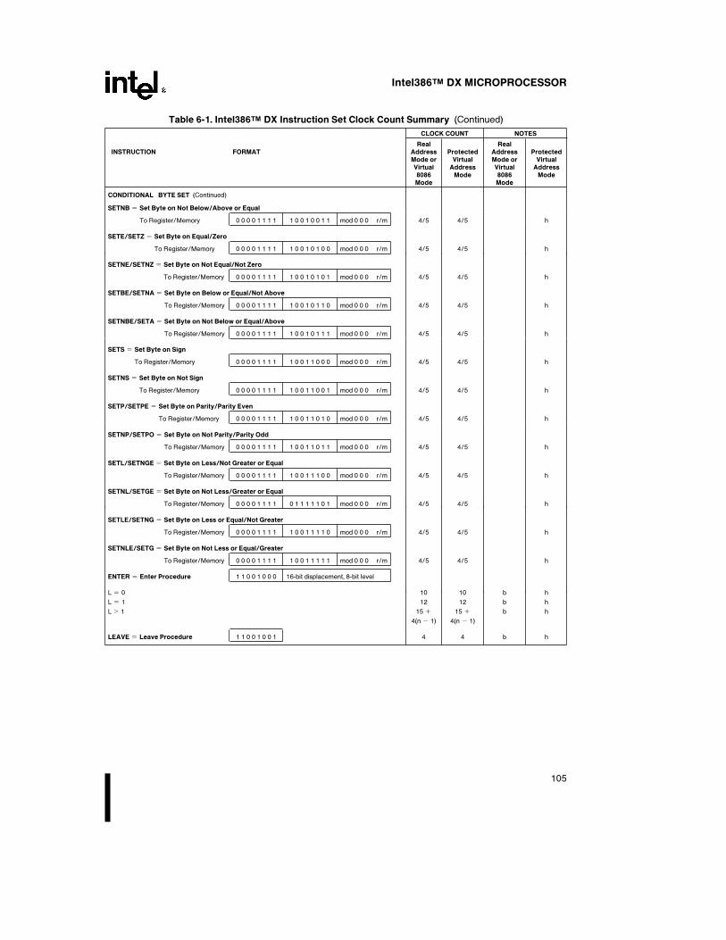
Intel386TM DX MICROPROCESSOR
Table 6-1. Intel386TM DX Instruction Set Clock Count Summary (Continued)
CLOCK COUNT NOTES
Real RealINSTRUCTION FORMAT Address Protected Address Protected
Mode or Virtual Mode or VirtualVirtual Address Virtual Address8086 Mode 8086 ModeMode Mode
CONDITIONAL BYTE SET (Continued)
SETNB e Set Byte on Not Below/Above or Equal
To Register/Memory 0 0 0 0 1 1 1 1 1 0 0 1 0 0 1 1 mod 0 0 0 r/m 4/5 4/5 h
SETE/SETZ e Set Byte on Equal/Zero
To Register/Memory 0 0 0 0 1 1 1 1 1 0 0 1 0 1 0 0 mod 0 0 0 r/m 4/5 4/5 h
SETNE/SETNZ e Set Byte on Not Equal/Not Zero
To Register/Memory 0 0 0 0 1 1 1 1 1 0 0 1 0 1 0 1 mod 0 0 0 r/m 4/5 4/5 h
SETBE/SETNA e Set Byte on Below or Equal/Not Above
To Register/Memory 0 0 0 0 1 1 1 1 1 0 0 1 0 1 1 0 mod 0 0 0 r/m 4/5 4/5 h
SETNBE/SETA e Set Byte on Not Below or Equal/Above
To Register/Memory 0 0 0 0 1 1 1 1 1 0 0 1 0 1 1 1 mod 0 0 0 r/m 4/5 4/5 h
SETS e Set Byte on Sign
To Register/Memory 0 0 0 0 1 1 1 1 1 0 0 1 1 0 0 0 mod 0 0 0 r/m 4/5 4/5 h
SETNS e Set Byte on Not Sign
To Register/Memory 0 0 0 0 1 1 1 1 1 0 0 1 1 0 0 1 mod 0 0 0 r/m 4/5 4/5 h
SETP/SETPE e Set Byte on Parity/Parity Even
To Register/Memory 0 0 0 0 1 1 1 1 1 0 0 1 1 0 1 0 mod 0 0 0 r/m 4/5 4/5 h
SETNP/SETPO e Set Byte on Not Parity/Parity Odd
To Register/Memory 0 0 0 0 1 1 1 1 1 0 0 1 1 0 1 1 mod 0 0 0 r/m 4/5 4/5 h
SETL/SETNGE e Set Byte on Less/Not Greater or Equal
To Register/Memory 0 0 0 0 1 1 1 1 1 0 0 1 1 1 0 0 mod 0 0 0 r/m 4/5 4/5 h
SETNL/SETGE e Set Byte on Not Less/Greater or Equal
To Register/Memory 0 0 0 0 1 1 1 1 0 1 1 1 1 1 0 1 mod 0 0 0 r/m 4/5 4/5 h
SETLE/SETNG e Set Byte on Less or Equal/Not Greater
To Register/Memory 0 0 0 0 1 1 1 1 1 0 0 1 1 1 1 0 mod 0 0 0 r/m 4/5 4/5 h
SETNLE/SETG e Set Byte on Not Less or Equal/Greater
To Register/Memory 0 0 0 0 1 1 1 1 1 0 0 1 1 1 1 1 mod 0 0 0 r/m 4/5 4/5 h
ENTER e Enter Procedure 1 1 0 0 1 0 0 0 16-bit displacement, 8-bit level
L e 0 10 10 b h
L e 1 12 12 b h
L l 1 15 a 15 a b h
4(n b 1) 4(n b 1)
LEAVE e Leave Procedure 1 1 0 0 1 0 0 1 4 4 b h
105
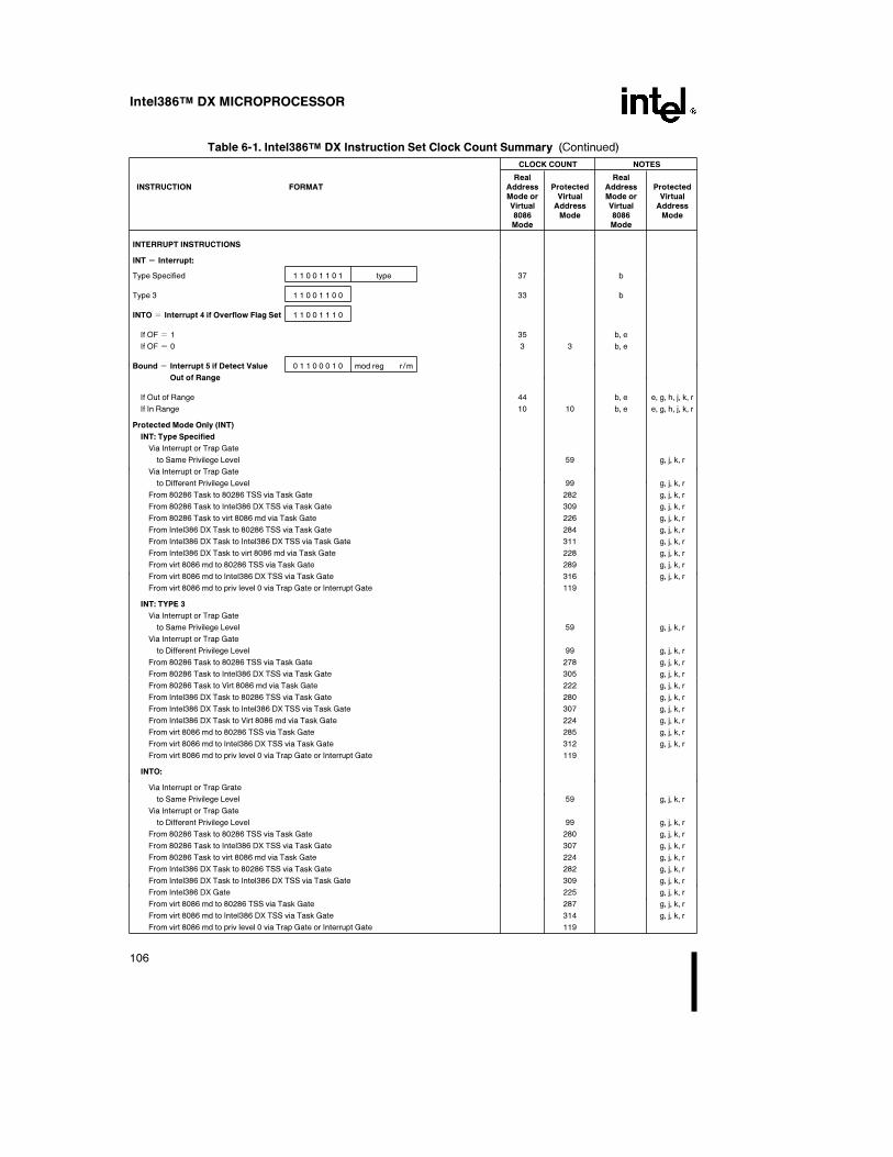
Intel386TM DX MICROPROCESSOR
Table 6-1. Intel386TM DX Instruction Set Clock Count Summary (Continued)
CLOCK COUNT NOTES
Real RealINSTRUCTION FORMAT Address Protected Address Protected
Mode or Virtual Mode or VirtualVirtual Address Virtual Address8086 Mode 8086 ModeMode Mode
INTERRUPT INSTRUCTIONS
INT e Interrupt:
Type Specified 1 1 0 0 1 1 0 1 type 37 b
Type 3 1 1 0 0 1 1 0 0 33 b
INTO e Interrupt 4 if Overflow Flag Set 1 1 0 0 1 1 1 0
If OF e 1 35 b, e
If OF e 0 3 3 b, e
Bound e Interrupt 5 if Detect Value 0 1 1 0 0 0 1 0 mod reg r/m
Out of Range
If Out of Range 44 b, e e, g, h, j, k, r
If In Range 10 10 b, e e, g, h, j, k, r
Protected Mode Only (INT)
INT: Type Specified
Via Interrupt or Trap Gate
to Same Privilege Level 59 g, j, k, r
Via Interrupt or Trap Gate
to Different Privilege Level 99 g, j, k, r
From 80286 Task to 80286 TSS via Task Gate 282 g, j, k, r
From 80286 Task to Intel386 DX TSS via Task Gate 309 g, j, k, r
From 80286 Task to virt 8086 md via Task Gate 226 g, j, k, r
From Intel386 DX Task to 80286 TSS via Task Gate 284 g, j, k, r
From Intel386 DX Task to Intel386 DX TSS via Task Gate 311 g, j, k, r
From Intel386 DX Task to virt 8086 md via Task Gate 228 g, j, k, r
From virt 8086 md to 80286 TSS via Task Gate 289 g, j, k, r
From virt 8086 md to Intel386 DX TSS via Task Gate 316 g, j, k, r
From virt 8086 md to priv level 0 via Trap Gate or Interrupt Gate 119
INT: TYPE 3
Via Interrupt or Trap Gate
to Same Privilege Level 59 g, j, k, r
Via Interrupt or Trap Gate
to Different Privilege Level 99 g, j, k, r
From 80286 Task to 80286 TSS via Task Gate 278 g, j, k, r
From 80286 Task to Intel386 DX TSS via Task Gate 305 g, j, k, r
From 80286 Task to Virt 8086 md via Task Gate 222 g, j, k, r
From Intel386 DX Task to 80286 TSS via Task Gate 280 g, j, k, r
From Intel386 DX Task to Intel386 DX TSS via Task Gate 307 g, j, k, r
From Intel386 DX Task to Virt 8086 md via Task Gate 224 g, j, k, r
From virt 8086 md to 80286 TSS via Task Gate 285 g, j, k, r
From virt 8086 md to Intel386 DX TSS via Task Gate 312 g, j, k, r
From virt 8086 md to priv level 0 via Trap Gate or Interrupt Gate 119
INTO:
Via Interrupt or Trap Grate
to Same Privilege Level 59 g, j, k, r
Via Interrupt or Trap Gate
to Different Privilege Level 99 g, j, k, r
From 80286 Task to 80286 TSS via Task Gate 280 g, j, k, r
From 80286 Task to Intel386 DX TSS via Task Gate 307 g, j, k, r
From 80286 Task to virt 8086 md via Task Gate 224 g, j, k, r
From Intel386 DX Task to 80286 TSS via Task Gate 282 g, j, k, r
From Intel386 DX Task to Intel386 DX TSS via Task Gate 309 g, j, k, r
From Intel386 DX Gate 225 g, j, k, r
From virt 8086 md to 80286 TSS via Task Gate 287 g, j, k, r
From virt 8086 md to Intel386 DX TSS via Task Gate 314 g, j, k, r
From virt 8086 md to priv level 0 via Trap Gate or Interrupt Gate 119
106

Intel386TM DX MICROPROCESSOR
Table 6-1. Intel386TM DX Instruction Set Clock Count Summary (Continued)
CLOCK COUNT NOTES
Real RealINSTRUCTION FORMAT Address Protected Address Protected
Mode or Virtual Mode or VirtualVirtual Address Virtual Address8086 Mode 8086 ModeMode Mode
INTERRUPT INSTRUCTIONS (Continued)
BOUND:
Via Interrupt or Trap Gate
to Same Privilege Level 59 g, j, k, r
Via Interrupt or Trap Gate
to Different Privilege Level 99 g, j, k, r
From 80286 Task to 80286 TSS via Task Gate 254 g, j, k, r
From 80286 Task to Intel386 DX TSS via Task Gate 284 g, j, k, r
From 80268 Task to virt 8086 Mode via Task Gate 231 g, j, k, r
From Intel386 DX Task to 80286 TSS via Task Gate 264 g, j, k, r
From Intel386 DX Task to Intel386 DX TSS via Task Gate 294 g, j, k, r
From 80368 Task to virt 8086 Mode via Task Gate 243 g, j, k, r,
From virt 8086 Mode to 80286 TSS via Task Gate 264 g, j, k, r
From virt 8086 Mode to Intel386 DX TSS via Task Gate 294 g, j, k, r
From virt 8086 md to priv level 0 via Trap Gate or Interrupt Gate 119
INTERRUPT RETURN
IRET e Interrupt Return 1 1 0 0 1 1 1 1 22 g, h, j, k, r
Protected Mode Only (IRET)
To the Same Privilege Level (within task) 38 g, h, j, k, r
To Different Privilege Level (within task) 82 g, h, j, k, r
From 80286 Task to 80286 TSS 232 h, j, k, r
From 80286 Task to Intel386 DX TSS 265 h, j, k, r
From 80286 Task to Virtual 8086 Task 213 h, j, k, r
From 80286 Task to Virtual 8086 Mode (within task) 60
From Intel386 DX Task to 80286 TSS 271 h, j, k, r
From Intel386 DX Task to Intel386 DX TSS 275 h, j, k, r
From Intel386 DX Task to Virtual 8086 Task 223 h, j, k, r
From Intel386 DX Task to Virtual 8086 Mode (within task) 60
PROCESSOR CONTROL
HLT e HALT 1 1 1 1 0 1 0 0 5 5 l
MOV e Move to and From Control/Debug/Test Registers
CR0/CR2/CR3 from register 0 0 0 0 1 1 1 1 0 0 1 0 0 0 1 0 1 1 eee reg 11/4/5 11/4/5 l
Register From CR0–3 0 0 0 0 1 1 1 1 0 0 1 0 0 0 0 0 1 1 eee reg 6 6 l
DR0–3 From Register 0 0 0 0 1 1 1 1 0 0 1 0 0 0 1 1 1 1 eee reg 22 22 l
DR6–7 From Register 0 0 0 0 1 1 1 1 0 0 1 0 0 0 1 1 1 1 eee reg 16 16 l
Register from DR6–7 0 0 0 0 1 1 1 1 0 0 1 0 0 0 0 1 1 1 eee reg 14 14 l
Register from DR0–3 0 0 0 0 1 1 1 1 0 0 1 0 0 0 0 1 1 1 eee reg 22 22 l
TR6–7 from Register 0 0 0 0 1 1 1 1 0 0 1 0 0 1 1 0 1 1 eee reg 12 12 l
Register from TR6–7 0 0 0 0 1 1 1 1 0 0 1 0 0 1 0 0 1 1 eee reg 12 12 l
NOP e No Operation 1 0 0 1 0 0 0 0 3 3
WAITeWait until BUSYÝ pin is negated 1 0 0 1 1 0 1 1 7 7
107
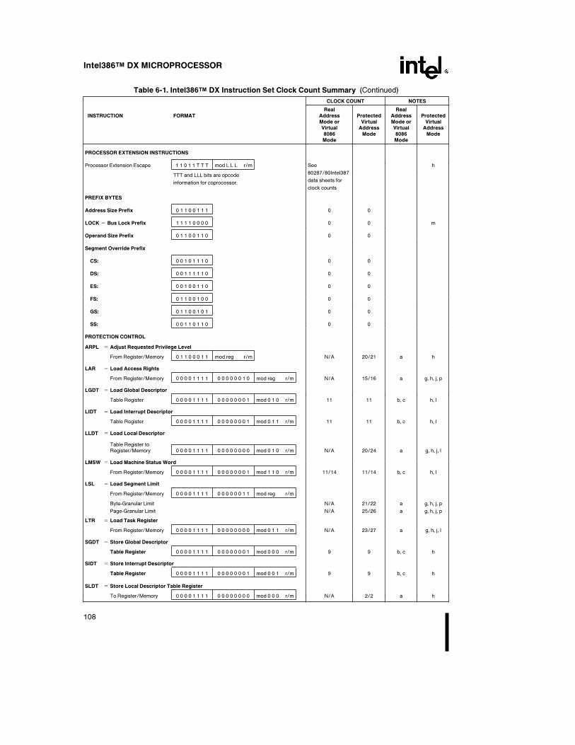
Intel386TM DX MICROPROCESSOR
Table 6-1. Intel386TM DX Instruction Set Clock Count Summary (Continued)
CLOCK COUNT NOTES
Real RealINSTRUCTION FORMAT Address Protected Address Protected
Mode or Virtual Mode or VirtualVirtual Address Virtual Address8086 Mode 8086 ModeMode Mode
PROCESSOR EXTENSION INSTRUCTIONS
Processor Extension Escape 1 1 0 1 1 T T T mod L L L r/m See h
TTT and LLL bits are opcode 80287/80Intel387
information for coprocessor. data sheets for
clock counts
PREFIX BYTES
Address Size Prefix 0 1 1 0 0 1 1 1 0 0
LOCK e Bus Lock Prefix 1 1 1 1 0 0 0 0 0 0 m
Operand Size Prefix 0 1 1 0 0 1 1 0 0 0
Segment Override Prefix
CS: 0 0 1 0 1 1 1 0 0 0
DS: 0 0 1 1 1 1 1 0 0 0
ES: 0 0 1 0 0 1 1 0 0 0
FS: 0 1 1 0 0 1 0 0 0 0
GS: 0 1 1 0 0 1 0 1 0 0
SS: 0 0 1 1 0 1 1 0 0 0
PROTECTION CONTROL
ARPL e Adjust Requested Privilege Level
From Register/Memory 0 1 1 0 0 0 1 1 mod reg r/m N/A 20/21 a h
LAR e Load Access Rights
From Register/Memory 0 0 0 0 1 1 1 1 0 0 0 0 0 0 1 0 mod reg r/m N/A 15/16 a g, h, j, p
LGDT e Load Global Descriptor
Table Register 0 0 0 0 1 1 1 1 0 0 0 0 0 0 0 1 mod 0 1 0 r/m 11 11 b, c h, l
LIDT e Load Interrupt Descriptor
Table Register 0 0 0 0 1 1 1 1 0 0 0 0 0 0 0 1 mod 0 1 1 r/m 11 11 b, c h, l
LLDT e Load Local Descriptor
Table Register toRegister/Memory 0 0 0 0 1 1 1 1 0 0 0 0 0 0 0 0 mod 0 1 0 r/m N/A 20/24 a g, h, j, l
LMSW e Load Machine Status Word
From Register/Memory 0 0 0 0 1 1 1 1 0 0 0 0 0 0 0 1 mod 1 1 0 r/m 11/14 11/14 b, c h, l
LSL e Load Segment Limit
From Register/Memory 0 0 0 0 1 1 1 1 0 0 0 0 0 0 1 1 mod reg r/m
Byte-Granular Limit N/A 21/22 a g, h, j, p
Page-Granular Limit N/A 25/26 a g, h, j, p
LTR e Load Task Register
From Register/Memory 0 0 0 0 1 1 1 1 0 0 0 0 0 0 0 0 mod 0 1 1 r/m N/A 23/27 a g, h, j, l
SGDT e Store Global Descriptor
Table Register 0 0 0 0 1 1 1 1 0 0 0 0 0 0 0 1 mod 0 0 0 r/m 9 9 b, c h
SIDT e Store Interrupt Descriptor
Table Register 0 0 0 0 1 1 1 1 0 0 0 0 0 0 0 1 mod 0 0 1 r/m 9 9 b, c h
SLDT e Store Local Descriptor Table Register
To Register/Memory 0 0 0 0 1 1 1 1 0 0 0 0 0 0 0 0 mod 0 0 0 r/m N/A 2/2 a h
108

Intel386TM DX MICROPROCESSOR
Table 6-1. Intel386TM DX Instruction Set Clock Count Summary (Continued)
CLOCK COUNT NOTES
Real RealINSTRUCTION FORMAT Address Protected Address Protected
Mode or Virtual Mode or VirtualVirtual Address Virtual Address8086 Mode 8086 ModeMode Mode
SMSW eStore MachineStatus Word 0 0 0 0 1 1 1 1 0 0 0 0 0 0 0 1 mod 1 0 0 r/m 2/2 2/2 b, c h, l
STR eStore Task Register
To Register/Memory 0 0 0 0 1 1 1 1 0 0 0 0 0 0 0 0 mod 0 0 1 r/m N/A 2/2 a h
VERR eVerify Read Accesss
Register/Memory 0 0 0 0 1 1 1 1 0 0 0 0 0 0 0 0 mod 1 0 0 r/m N/A 10/11 a g, h, j, p
VERW e Verify Write Accesss 0 0 0 0 1 1 1 1 0 0 0 0 0 0 0 0 mod 1 0 1 r/m N/A 15/16 a g, h, j, p
INSTRUCTION NOTES FOR TABLE 6-1
Notes a through c apply to Intel386 DX Real Address Mode only:a. This is a Protected Mode instruction. Attempted execution in Real Mode will result in exception 6 (invalid opcode).b. Exception 13 fault (general protection) will occur in Real Mode if an operand reference is made that partially or fullyextends beyond the maximum CS, DS, ES, FS or GS limit, FFFFH. Exception 12 fault (stack segment limit violation or notpresent) will occur in Real Mode if an operand reference is made that partially or fully extends beyond the maximum SS limit.c. This instruction may be executed in Real Mode. In Real Mode, its purpose is primarily to initialize the CPU for ProtectedMode.
Notes d through g apply to Intel386 DX Real Address Mode and Intel386 DX Protected Virtual Address Mode:d. The Intel386 DX uses an early-out multiply algorithm. The actual number of clocks depends on the position of the mostsignificant bit in the operand (multiplier).
Clock counts given are minimum to maximum. To calculate actual clocks use the following formula:Actual Clock e if m k l 0 then max ([log2 lml], 3) a b clocks:
if m e 0 then 3ab clocksIn this formula, m is the multiplier, andb e 9 for register to register,b e 12 for memory to register,b e 10 for register with immediate to register,b e 11 for memory with immediate to register.
e. An exception may occur, depending on the value of the operand.f. LOCKÝ is automatically asserted, regardless of the presence or absence of the LOCKÝ prefix.g. LOCKÝ is asserted during descriptor table accesses.
Notes h through r apply to Intel386 DX Protected Virtual Address Mode only:h. Exception 13 fault (general protection violation) will occur if the memory operand in CS, DS, ES, FS or GS cannot be useddue to either a segment limit violation or access rights violation. If a stack limit is violated, an exception 12 (stack segmentlimit violation or not present) occurs.i. For segment load operations, the CPL, RPL, and DPL must agree with the privilege rules to avoid an exception 13 fault(general protection violation). The segment’s descriptor must indicate ‘‘present’’ or exception 11 (CS, DS, ES, FS, GS notpresent). If the SS register is loaded and a stack segment not present is detected, an exception 12 (stack segment limitviolation or not present) occurs.j. All segment descriptor accesses in the GDT or LDT made by this instruction will automatically assert LOCKÝ to maintaindescriptor integrity in multiprocessor systems.k. JMP, CALL, INT, RET and IRET instructions referring to another code segment will cause an exception 13 (generalprotection violation) if an applicable privilege rule is violated.l. An exception 13 fault occurs if CPL is greater than 0 (0 is the most privileged level).m. An exception 13 fault occurs if CPL is greater than IOPL.n. The IF bit of the flag register is not updated if CPL is greater than IOPL. The IOPL and VM fields of the flag register areupdated only if CPL e 0.o. The PE bit of the MSW (CR0) cannot be reset by this instruction. Use MOV into CR0 if desiring to reset the PE bit.p. Any violation of privilege rules as applied to the selector operand does not cause a protection exception; rather, the zeroflag is cleared.q. If the coprocessor’s memory operand violates a segment limit or segment access rights, an exception 13 fault (generalprotection exception) will occur before the ESC instruction is executed. An exception 12 fault (stack segment limit violationor not present) will occur if the stack limit is violated by the operand’s starting address.r. The destination of a JMP, CALL, INT, RET or IRET must be in the defined limit of a code segment or an exception 13 fault(general protection violation) will occur.
109

Intel386TM DX MICROPROCESSOR
6.2 INSTRUCTION ENCODING
6.2.1 Overview
All instruction encodings are subsets of the generalinstruction format shown in Figure 6-1. Instructionsconsist of one or two primary opcode bytes, possiblyan address specifier consisting of the ‘‘mod r/m’’byte and ‘‘scaled index’’ byte, a displacement if re-quired, and an immediate data field if required.
Within the primary opcode or opcodes, smaller en-coding fields may be defined. These fields vary ac-cording to the class of operation. The fields definesuch information as direction of the operation, sizeof the displacements, register encoding, or sign ex-tension.
Almost all instructions referring to an operand inmemory have an addressing mode byte followingthe primary opcode byte(s). This byte, the mod r/mbyte, specifies the address mode to be used. Certain
encodings of the mod r/m byte indicate a secondaddressing byte, the scale-index-base byte, followsthe mod r/m byte to fully specify the addressingmode.
Addressing modes can include a displacement im-mediately following the mod r/m byte, or scaled in-dex byte. If a displacement is present, the possiblesizes are 8, 16 or 32 bits.
If the instruction specifies an immediate operand,the immediate operand follows any displacementbytes. The immediate operand, if specified, is alwaysthe last field of the instruction.
Figure 6-1 illustrates several of the fields that canappear in an instruction, such as the mod field andthe r/m field, but the Figure does not show all fields.Several smaller fields also appear in certain instruc-tions, sometimes within the opcode bytes them-selves. Table 6-2 is a complete list of all fields ap-pearing in the Intel386 DX instruction set. Furtherahead, following Table 6-2, are detailed tables foreach field.
T T T T T T T T T T T T T T T T mod T T T r/m ss index base d32 l 16 l 8 l none data32 l 16 l 8 l none
7 0 7 0 7 6 5 3 2 0 7 6 5 3 2 0X ä Y X ä Y X ä YX ä Y X ä Yopcode ‘‘mod r/m’’ ‘‘s-i-b’’ address immediate
(one or two bytes) byte byte displacement dataX ä Y(T represents an (4, 2, 1 bytes (4, 2, 1 bytes
opcode bit.) register and address or none) or none)
mode specifier
Figure 6-1. General Instruction Format
Table 6-2. Fields within Intel386TM DX Instructions
Field Name Description Number of Bits
w Specifies if Data is Byte or Full Size (Full Size is either 16 or 32 Bits 1
d Specifies Direction of Data Operation 1
s Specifies if an Immediate Data Field Must be Sign-Extended 1
reg General Register Specifier 3
mod r/m Address Mode Specifier (Effective Address can be a General Register) 2 for mod;
3 for r/m
ss Scale Factor for Scaled Index Address Mode 2
index General Register to be used as Index Register 3
base General Register to be used as Base Register 3
sreg2 Segment Register Specifier for CS, SS, DS, ES 2
sreg3 Segment Register Specifier for CS, SS, DS, ES, FS, GS 3
tttn For Conditional Instructions, Specifies a Condition Asserted
or a Condition Negated 4
Note: Table 6-1 shows encoding of individual instructions.
110

Intel386TM DX MICROPROCESSOR
6.2.2 32-Bit Extensions of theInstruction Set
With the Intel386 DX, the 8086/80186/80286 in-struction set is extended in two orthogonal direc-tions: 32-bit forms of all 16-bit instructions are addedto support the 32-bit data types, and 32-bit address-ing modes are made available for all instructions ref-erencing memory. This orthogonal instruction set ex-tension is accomplished having a Default (D) bit inthe code segment descriptor, and by having 2 prefix-es to the instruction set.
Whether the instruction defaults to operations of 16bits or 32 bits depends on the setting of the D bit inthe code segment descriptor, which gives the de-fault length (either 32 bits or 16 bits) for both oper-ands and effective addresses when executing thatcode segment. In the Real Address Mode or Virtual8086 Mode, no code segment descriptors are used,but a D value of 0 is assumed internally by the In-tel386 DX when operating in those modes (for 16-bitdefault sizes compatible with the 8086/80186/80286).
Two prefixes, the Operand Size Prefix and the Effec-tive Address Size Prefix, allow overriding individuallythe Default selection of operand size and effectiveaddress size. These prefixes may precede any op-code bytes and affect only the instruction they pre-cede. If necessary, one or both of the prefixes maybe placed before the opcode bytes. The presence ofthe Operand Size Prefix and the Effective AddressPrefix will toggle the operand size or the effectiveaddress size, respectively, to the value ‘‘opposite’’from the Default setting. For example, if the defaultoperand size is for 32-bit data operations, then pres-ence of the Operand Size Prefix toggles the instruc-tion to 16-bit data operation. As another example, ifthe default effective address size is 16 bits, pres-ence of the Effective Address Size prefix toggles theinstruction to use 32-bit effective address computa-tions.
These 32-bit extensions are available in all Intel386DX modes, including the Real Address Mode or theVirtual 8086 Mode. In these modes the default isalways 16 bits, so prefixes are needed to specify32-bit operands or addresses. For instructions withmore than one prefix, the order of prefixes is unim-portant.
Unless specified otherwise, instructions with 8-bitand 16-bit operands do not affect the contents ofthe high-order bits of the extended registers.
6.2.3 Encoding of Instruction Fields
Within the instruction are several fields indicatingregister selection, addressing mode and so on. Theexact encodings of these fields are defined immedi-ately ahead.
6.2.3.1 ENCODING OF OPERAND LENGTH (w)FIELD
For any given instruction performing a data opera-tion, the instruction is executing as a 32-bit operationor a 16-bit operation. Within the constraints of theoperation size, the w field encodes the operand sizeas either one byte or the full operation size, asshown in the table below.
Operand Size Operand Size
w Field During 16-Bit During 32-Bit
Data Operations Data Operations
0 8 Bits 8 Bits
1 16 Bits 32 Bits
6.2.3.2 ENCODING OF THE GENERALREGISTER (reg) FIELD
The general register is specified by the reg field,which may appear in the primary opcode bytes, or asthe reg field of the ‘‘mod r/m’’ byte, or as the r/mfield of the ‘‘mod r/m’’ byte.
Encoding of reg Field When w Field
is not Present in Instruction
Register Selected Register Selected
reg Field During 16-Bit During 32-Bit
Data Operations Data Operations
000 AX EAX
001 CX ECX
010 DX EDX
011 BX EBX
100 SP ESP
101 BP EBP
110 SI ESI
111 DI EDI
Encoding of reg Field When w Field
is Present in Instruction
Register Specified by reg Field
During 16-Bit Data Operations:
regFunction of w Field
(when w e 0) (when w e 1)
000 AL AX
001 CL CX
010 DL DX
011 BL BX
100 AH SP
101 CH BP
110 DH SI
111 BH DI
111
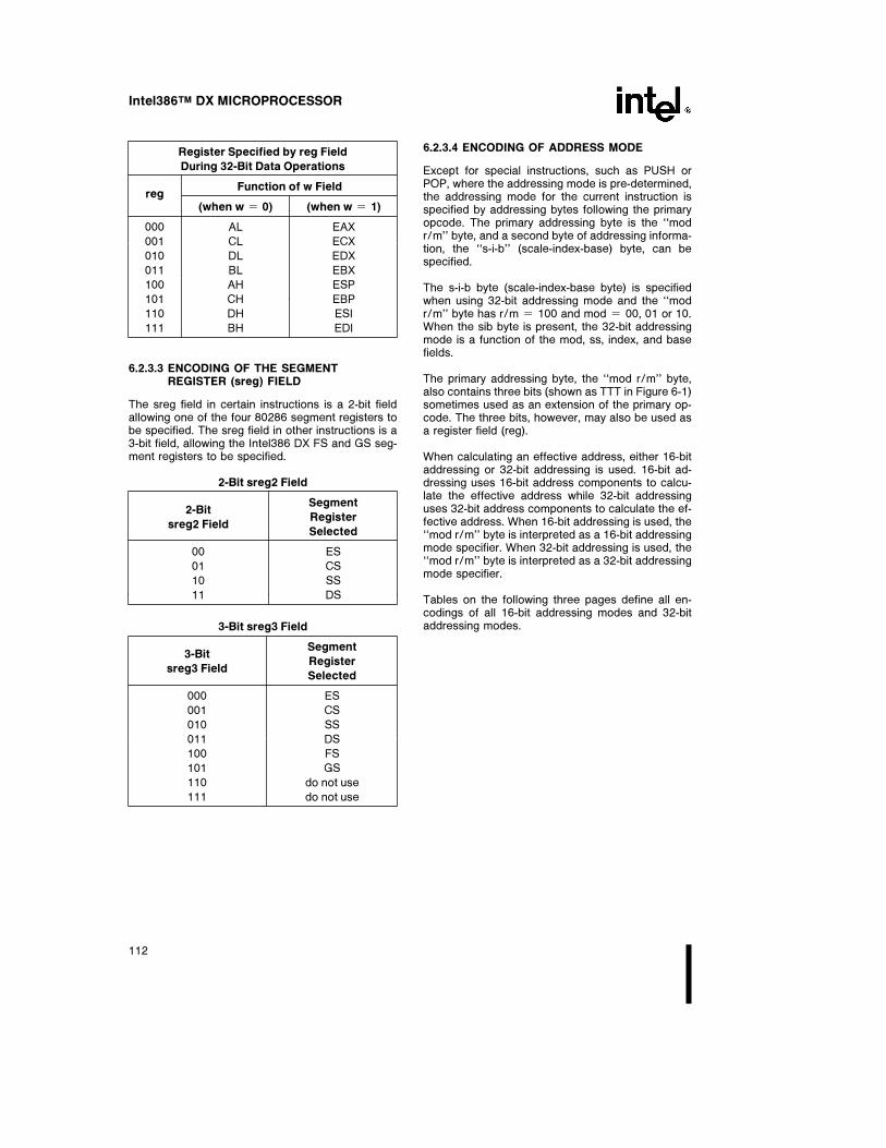
Intel386TM DX MICROPROCESSOR
Register Specified by reg Field
During 32-Bit Data Operations
regFunction of w Field
(when w e 0) (when w e 1)
000 AL EAX
001 CL ECX
010 DL EDX
011 BL EBX
100 AH ESP
101 CH EBP
110 DH ESI
111 BH EDI
6.2.3.3 ENCODING OF THE SEGMENTREGISTER (sreg) FIELD
The sreg field in certain instructions is a 2-bit fieldallowing one of the four 80286 segment registers tobe specified. The sreg field in other instructions is a3-bit field, allowing the Intel386 DX FS and GS seg-ment registers to be specified.
2-Bit sreg2 Field
2-BitSegment
sreg2 FieldRegister
Selected
00 ES
01 CS
10 SS
11 DS
3-Bit sreg3 Field
3-BitSegment
sreg3 FieldRegister
Selected
000 ES
001 CS
010 SS
011 DS
100 FS
101 GS
110 do not use
111 do not use
6.2.3.4 ENCODING OF ADDRESS MODE
Except for special instructions, such as PUSH orPOP, where the addressing mode is pre-determined,the addressing mode for the current instruction isspecified by addressing bytes following the primaryopcode. The primary addressing byte is the ‘‘modr/m’’ byte, and a second byte of addressing informa-tion, the ‘‘s-i-b’’ (scale-index-base) byte, can bespecified.
The s-i-b byte (scale-index-base byte) is specifiedwhen using 32-bit addressing mode and the ‘‘modr/m’’ byte has r/m e 100 and mod e 00, 01 or 10.When the sib byte is present, the 32-bit addressingmode is a function of the mod, ss, index, and basefields.
The primary addressing byte, the ‘‘mod r/m’’ byte,also contains three bits (shown as TTT in Figure 6-1)sometimes used as an extension of the primary op-code. The three bits, however, may also be used asa register field (reg).
When calculating an effective address, either 16-bitaddressing or 32-bit addressing is used. 16-bit ad-dressing uses 16-bit address components to calcu-late the effective address while 32-bit addressinguses 32-bit address components to calculate the ef-fective address. When 16-bit addressing is used, the‘‘mod r/m’’ byte is interpreted as a 16-bit addressingmode specifier. When 32-bit addressing is used, the‘‘mod r/m’’ byte is interpreted as a 32-bit addressingmode specifier.
Tables on the following three pages define all en-codings of all 16-bit addressing modes and 32-bitaddressing modes.
112

Intel386TM DX MICROPROCESSOR
Encoding of 16-bit Address Mode with ‘‘mod r/m’’ Byte
mod r/m Effective Address
00 000 DS:[BXaSI]00 001 DS:[BXaDI]00 010 SS:[BPaSI]00 011 SS:[BPaDI]00 100 DS:[SI]00 101 DS:[DI]00 110 DS:d16
00 111 DS:[BX]
01 000 DS:[BXaSIad8]01 001 DS:[BXaDIad8]01 010 SS:[BPaSIad8]01 011 SS:[BPaDIad8]01 100 DS:[SIad8]01 101 DS:[DIad8]01 110 SS:[BPad8]01 111 DS:[BXad8]
mod r/m Effective Address
10 000 DS:[BXaSIad16]10 001 DS:[BXaDIad16]10 010 SS:[BPaSIad16]10 011 SS:[BPaDIad16]10 100 DS:[SIad16]10 101 DS:[DIad16]10 110 SS:[BPad16]10 111 DS:[BXad16]
11 000 registerÐsee below
11 001 registerÐsee below
11 010 registerÐsee below
11 011 registerÐsee below
11 100 registerÐsee below
11 101 registerÐsee below
11 110 registerÐsee below
11 111 registerÐsee below
Register Specified by r/m
During 16-Bit Data Operations
mod r/mFunction of w Field
(when we0) (when w e1)
11 000 AL AX
11 001 CL CX
11 010 DL DX
11 011 BL BX
11 100 AH SP
11 101 CH BP
11 110 DH SI
11 111 BH DI
Register Specified by r/m
During 32-Bit Data Operations
mod r/mFunction of w Field
(when we0) (when w e1)
11 000 AL EAX
11 001 CL ECX
11 010 DL EDX
11 011 BL EBX
11 100 AH ESP
11 101 CH EBP
11 110 DH ESI
11 111 BH EDI
113

Intel386TM DX MICROPROCESSOR
Encoding of 32-bit Address Mode with ‘‘mod r/m’’ byte (no ‘‘s-i-b’’ byte present):
mod r/m Effective Address
00 000 DS:[EAX]00 001 DS:[ECX]00 010 DS:[EDX]00 011 DS:[EBX]00 100 s-i-b is present
00 101 DS:d32
00 110 DS:[ESI]00 111 DS:[EDI]
01 000 DS:[EAXad8]01 001 DS:[ECXad8]01 010 DS:[EDXad8]01 011 DS:[EBXad8]01 100 s-i-b is present
01 101 SS:[EBPad8]01 110 DS:[ESIad8]01 111 DS:[EDIad8]
mod r/m Effective Address
10 000 DS:[EAXad32]10 001 DS:[ECXad32]10 010 DS:[EDXad32]10 011 DS:[EBXad32]10 100 s-i-b is present
10 101 SS:[EBPad32]10 110 DS:[ESIad32]10 111 DS:[EDIad32]
11 000 registerÐsee below
11 001 registerÐsee below
11 010 registerÐsee below
11 011 registerÐsee below
11 100 registerÐsee below
11 101 registerÐsee below
11 110 registerÐsee below
11 111 registerÐsee below
Register Specified by reg or r/m
during 16-Bit Data Operations:
mod r/mfunction of w field
(when we0) (when we1)
11 000 AL AX
11 001 CL CX
11 010 DL DX
11 011 BL BX
11 100 AH SP
11 101 CH BP
11 110 DH SI
11 111 BH DI
Register Specified by reg or r/m
during 32-Bit Data Operations:
mod r/mfunction of w field
(when we0) (when we1)
11 000 AL EAX
11 001 CL ECX
11 010 DL EDX
11 011 BL EBX
11 100 AH ESP
11 101 CH EBP
11 110 DH ESI
11 111 BH EDI
114

Intel386TM DX MICROPROCESSOR
Encoding of 32-bit Address Mode (‘‘mod r/m’’ byte and ‘‘s-i-b’’ byte present):
mod base Effective Address
00 000 DS:[EAX a (scaled index)]00 001 DS:[ECX a (scaled index)]00 010 DS:[EDX a (scaled index)]00 011 DS:[EBX a (scaled index)]00 100 SS:[ESP a (scaled index)]00 101 DS:[d32 a (scaled index)]00 110 DS:[ESI a (scaled index)]00 111 DS:[EDI a (scaled index)]
01 000 DS:[EAX a (scaled index) a d8]01 001 DS:[ECX a (scaled index) a d8]01 010 DS:[EDX a (scaled index) a d8]01 011 DS:[EBX a (scaled index) a d8]01 100 SS:[ESP a (scaled index) a d8]01 101 SS:[EBP a (scaled index) a d8]01 110 DS:[ESI a (scaled index) a d8]01 111 DS:[EDI a (scaled index) a d8]
10 000 DS:[EAX a (scaled index) a d32]10 001 DS:[ECX a (scaled index) a d32]10 010 DS:[EDX a (scaled index) a d32]10 011 DS:[EBX a (scaled index) a d32]10 100 SS:[ESP a (scaled index) a d32]10 101 SS:[EBP a (scaled index) a d32]10 110 DS:[ESI a (scaled index) a d32]10 111 DS:[EDI a (scaled index) a d32]
NOTE:Mod field in ‘‘mod r/m’’ byte; ss, index, base fields in‘‘s-i-b’’ byte.
ss Scale Factor
00 x1
01 x2
10 x4
11 x8
index Index Register
000 EAX
001 ECX
010 EDX
011 EBX
100 no index reg**101 EBP
110 ESI
111 EDI
**IMPORTANT NOTE:When index field is 100, indicating ‘‘no index register,’’ thenss field MUST equal 00. If index is 100 and ss does notequal 00, the effective address is undefined.
115

Intel386TM DX MICROPROCESSOR
6.2.3.5 ENCODING OF OPERATION DIRECTION(d) FIELD
In many two-operand instructions the d field is pres-ent to indicate which operand is considered thesource and which is the destination.
d Direction of Operation
0 Register/Memory k- - Register‘‘reg’’ Field Indicates Source Operand;‘‘mod r/m’’ or ‘‘mod ss index base’’ IndicatesDestination Operand
1 Register k- - Register/Memory‘‘reg’’ Field Indicates Destination Operand;‘‘mod r/m’’ or ‘‘mod ss index base’’ IndicatesSource Operand
6.2.3.6 ENCODING OF SIGN-EXTEND (s) FIELD
The s field occurs primarily to instructions with im-mediate data fields. The s field has an effect only ifthe size of the immediate data is 8 bits and is beingplaced in a 16-bit or 32-bit destination.
sEffect on Effect on
Immediate Data8 Immediate Data 16l32
0 None None
1 Sign-Extend Data8 to Fill None16-Bit or 32-Bit Destination
6.2.3.7 ENCODING OF CONDITIONAL TEST(tttn) FIELD
For the conditional instructions (conditional jumpsand set on condition), tttn is encoded with n indicat-ing to use the condition (ne0) or its negation (ne1),and ttt giving the condition to test.
Mnemonic Condition tttn
O Overflow 0000NO No Overflow 0001B/NAE Below/Not Above or Equal 0010NB/AE Not Below/Above or Equal 0011E/Z Equal/Zero 0100NE/NZ Not Equal/Not Zero 0101BE/NA Below or Equal/Not Above 0110NBE/A Not Below or Equal/Above 0111S Sign 1000NS Not Sign 1001P/PE Parity/Parity Even 1010NP/PO Not Parity/Parity Odd 1011L/NGE Less Than/Not Greater or Equal 1100NL/GE Not Less Than/Greater or Equal 1101LE/NG Less Than or Equal/Greater Than 1110NLE/G Not Less or Equal/Greater Than 1111
6.2.3.8 ENCODING OF CONTROL OR DEBUGOR TEST REGISTER (eee) FIELD
For the loading and storing of the Control, Debugand Test registers.
When Interpreted as Control Register Field
eee Code Reg Name
000 CR0010 CR2011 CR3
Do not use any other encoding
When Interpreted as Debug Register Field
eee Code Reg Name
000 DR0001 DR1010 DR2011 DR3110 DR6111 DR7
Do not use any other encoding
When Interpreted as Test Register Field
eee Code Reg Name
110 TR6111 TR7
Do not use any other encoding
116

Intel386TM DX MICROPROCESSOR
231630–84
Figure 7-1. Processor Module Dimensions
7. DESIGNING FOR ICETM-Intel386DX EMULATOR USE
The Intel386 DX in-circuit emulator products areICE-Intel386 DX 25 MHz or 33 MHz (both referred toas ICE-Intel386 DX emulator). The ICE-Intel386 DXemulator probe module has several electrical andmechanical characteristics that should be taken intoconsideration when designing the hardware.
Capacitive loading: The ICE-Intel386 DX emulatoradds up to 25 pF to each line.
Drive requirement: The ICE-Intel386 DX emulatoradds one standard TTL load on the CLK2 line, up toone advanced low-power Schottky TTL load percontrol signal line, and one advanced low-powerSchottky TTL load per address, byte enable, anddata line. These loads are within the probe moduleand are driven by the probe’s Intel386 DX compo-nent, which has standard drive and loading capabili-ty listed in the A.C. and D.C. Specification Tables inSections 9.4 and 9.5.
Power requirement: For noise immunity the ICE-In-tel386 DX emulator probe is powered by the usersystem. This high-speed probe circuitry draws up to1.5A plus the maximum ICC from the user Intel386DX component socket.
Intel386 DX location and orientation: The ICE-In-tel386 DX processor module, target-adaptor cable(which does not exist for the ICE-Intel386 DX33 MHz emulator), and the isolation board used forextra electrical buffering of the emulator initially, re-quire clearance as illustrated in Figures 7-1 and 7-2.
Interface Board and CLK2 speed reduction:When the ICE-Intel386 DX emulator probe is firstattached to an unverified user system, the interfaceboard helps the ICE-Intel386 DX emulator functionin user systems with bus faults (shorted signals,etc.). After electrical verification it may be removed.Only when the interface board is installed, the usersystem must have a reduced CLK2 frequency of25 MHz maximum.
Cache coherence: The ICE-Intel386 DX emulatorloads user memory by performing Intel386 DX com-ponent write cycles. Note that if the user system isnot designed to update or invalidate its cache (if ithas a cache) upon processor writes to memory, thecache could contain stale instruction code and/ordata. For best use of the ICE-Intel386 DX emulator,the user should consider designing the cache (if any)to update itself automatically when processor writesoccur, or find another method of maintaining cachedata coherence with main user memory.
117

Intel386TM DX MICROPROCESSOR
231630–85
Figure 7-2. Processor Module, Target-Adapter Cable, and Isolation Board Dimensions
118

Intel386TM DX MICROPROCESSOR
8. MECHANICAL DATA
8.1 INTRODUCTION
In this section, the physical packaging and its con-nections are described in detail.
8.2 PACKAGE DIMENSIONS ANDMOUNTING
The initial Intel386 DX package is a 132-pin ceramicpin grid array (PGA). Pins of this package are ar-ranged 0.100 inch (2.54mm) center-to-center, in a14 x 14 matrix, three rows around.
A wide variety of available sockets allow low inser-tion force or zero insertion force mountings, and achoice of terminals such as soldertail, surfacemount, or wire wrap. Several applicable sockets arelisted in Table 8.1.
231630–35
Figure 8.1. 132-Pin Ceramic PGA Package Dimensions
119

Intel386TM DX MICROPROCESSOR
Table 8.1. Several Socket Options for 132-Pin PGA
* Low insertion force (LIF) soldertail55274-1
* Amp tests indicate 50% reduction in insertionforce compared to machined sockets
Other socket options* Zero insertion force (ZIF) soldertail
55583-1* Zero insertion force (ZIF) Burn-in version
55573-2
Amp Incorporated(Harrisburg, PA 17105 U.S.A.Phone 717-564-0100)
231630–45Cam handle locks in low profile position when substrate is installed (handle UP foropen and DOWN for closed positions)
courtesy Amp Incorporated
Peel-A-Way Mylar and KaptonSocket Terminal Carriers
* Low insertion force surfacemount CS132-37TG
* Low insertion force soldertailCS132-01TG
* Low insertion force wire-wrapCS132-02TG (two level)CS132-03TG (three-level)
* Low insertion force press-fitCS132-05TG
Advanced Interconnections(5 Division StreetWarwick, RI 02818 U.S.A.Phone 401-885-0485)
Peel-A-Way Carrier No. 132:Kapton Carrier is KS132Mylar Carrier is MS132
Molded Plastic Body KS132is shown below:
231630–46
231630–47courtesy Advanced Interconnections
(Peel-A-Way Terminal CarriersU.S. Patent No. 4442938)
120

Intel386TM DX MICROPROCESSOR
Table 8.1. Several Socket Options for 132-Pin PGA (Continued)
PIN GRID ARRAYDECOUPLING SOCKETS
* Low insertion force soldertail0.125 length PGD-005-1A1Finish: Term/Contact Tin-Lead/Gold
* Low insertion force soldertail0.180 length PGD-005-1B1Finish: Term/Contact: Tin-Lead/Gold
* Low insertion 3 level Wire/Wrap PGD-005-1C1 Finish:Term/Contact Tin-Lead/Gold
Includes 0.10 mF & 1.0 mFDecoupling Capacitors
AUGAT INC.33 Perry Ave., P.O. Box 779 Attleboro, MA 02703TECHNICAL INFORMATION: (508) 222-2202CUSTOMER SERVICE: (508) 699-9800
VisinPak Kapton Carrier
PKC Series
Pin Grid Array
PGM (Plastic) or PPS(Glass Epoxy) Series
231630–86
* Low insertion force socket soldertail(for production use)2XX-6576-00-3308 (new style)2XX-6003-00-3302 (older style)
* Zero insertion force soldertail(for test and burn-in use)2XX-6568-00-3302
Textool ProductsElectronic Products Division/3M
(1410 West Pioneer DriveIrving, Texas 75601 U.S.A.Phone 214-259-2676)
courtesy Textool Products/3M 231630–48
121

Intel386TM DX MICROPROCESSOR
8.3 PACKAGE THERMALSPECIFICATION
The Intel386 DX is specified for operation whencase temperature is within the range of 0§C–85§C.The case temperature may be measured in any envi-ronment, to determine whether the Intel386 DX iswithin specified operating range.
The PGA case temperature should be measured atthe center of the top surface opposite the pins, as inFigure 8.2.
231630–36
Figure 8.2. Measuring Intel386TM DX PGA Case Temperature
Table 8.2. Intel386TM DX PGA Package Thermal Characteristics
Thermal Resistance Ð §C/Watt
Airflow Ð ft./min (m/sec)
Parameter 0 50 100 200 400 600 800(0) (0.25) (0.50) (1.01) (2.03) (3.04) (4.06)
i Junction-to-Case 2 2 2 2 2 2 2(case measuredas Fig. 8-2)
i Case-to-Ambient 19 18 17 15 12 10 9(no heatsink)
i Case-to-Ambient 16 15 14 12 9 7 6(with omnidirectionalheatsink)
i Case-to-Ambient 15 14 13 11 8 6 5(with unidirectionalheatsink)
NOTES:1. Table 8.2 applies to Intel386TM DX PGAplugged into socket or soldered directlyinto board.2. iJA e iJC a iCA.
3. iJ-CAP e 4§C/w (approx.)iJ-PIN e 4§C/w (inner pins) (approx.)iJ-PIN e 8§C/w (outer pins) (approx.)
4. TA e TC b P * iCA (ambient temperature)
231630–72
122
Intel386TM DX MICROPROCESSOR
9. ELECTRICAL DATA
9.1 INTRODUCTION
The following sections describe recommended elec-trical connections for the Intel386 DX, and its electri-cal specifications.
9.2 POWER AND GROUNDING
9.2.1 Power Connections
The Intel386 DX is implemented in CHMOS III andCHMOS IV technology and has modest power re-quirements. However, its high clock frequency and72 output buffers (address, data, control, and HLDA)can cause power surges as multiple output buffersdrive new signal levels simultaneously. For clean on-chip power distribution at high frequency, 20 VCCand 21 VSS pins separately feed functional units ofthe Intel386 DX.
Power and ground connections must be made to allexternal VCC and GND pins of the Intel386 DX. Onthe circuit board, all VCC pins must be connected ona VCC plane. All VSS pins must be likewise connect-ed on a GND plane.
9.2.2 Power DecouplingRecommendations
Liberal decoupling capacitance should be placednear the Intel386 DX. The Intel386 DX driving its32-bit parallel address and data buses at high fre-quencies can cause transient power surges, particu-larly when driving large capacitive loads.
Low inductance capacitors and interconnects arerecommended for best high frequency electrical per-formance. Inductance can be reduced by shorteningcircuit board traces between the Intel386 DX and
decoupling capacitors as much as possible. Capaci-tors specifically for PGA packages are also commer-cially available, for the lowest possible inductance.
9.2.3 Resistor Recommendations
The ERRORÝ and BUSYÝ inputs have resistor pull-ups of approximately 20 KX built-in to the Intel386DX to keep these signals negated when no Intel387DX coprocessor is present in the system (or tempo-rarily removed from its socket). The BS16Ý inputalso has an internal pullup resistor of approximately20 KX, and the PEREQ input has an internal pull-down resistor of approximately 20 KX.
In typical designs, the external pullup resistorsshown in Table 9-1 are recommended. However, aparticular design may have reason to adjust the re-sistor values recommended here, or alter the use ofpullup resistors in other ways.
9.2.4 Other ConnectionRecommendations
For reliable operation, always connect unused in-puts to an appropriate signal level. N.C. pins shouldalways remain unconnected.
Particularly when not using interrupts or bus hold,(as when first prototyping, perhaps) prevent anychance of spurious activity by connecting these as-sociated inputs to GND:
Pin Signal
B7 INTRB8 NMID14 HOLD
If not using address pipelining, pullup D13 NAÝ toVCC.
If not using 16-bit bus size, pullup C14 BS16Ý toVCC.
Pullups in the range of 20 KX are recommended.
Table 9-1. Recommended Resistor Pullups to VCC
Pin and Signal Pullup Value Purpose
E14 ADSÝ 20 KX g10% Lightly Pull ADSÝ Negated
During Intel386 DX Hold
Acknowledge States
C10 LOCKÝ 20 KX g10% Lightly Pull LOCKÝ Negated
During Intel386 DX Hold
Acknowledge States
123
Intel386TM DX MICROPROCESSOR
9.3 MAXIMUM RATINGS
Table 9-2. Maximum Ratings
Intel386TM DX
Parameter 20, 25, 33 MHz
Maximum Rating
Storage Temperature b65§C to a150§CCase Temperature Under Bias b65§C to a110§CSupply Voltage with Respect to VSS b0.5V to a6.5V
Voltage on Other Pins b0.5V to VCC a 0.5V
Table 9-2 is a stress rating only, and functional oper-ation at the maximums is not guaranteed. Functionaloperating conditions are given in 9.4 D.C. Specifica-tions and 9.5 A.C. Specifications.
Extended exposure to the Maximum Ratings may af-fect device reliability. Furthermore, although the In-tel386 DX contains protective circuitry to resist dam-age from static electric discharge, always take pre-cautions to avoid high static voltages or electricfields.
9.4 D.C. SPECIFICATIONSFunctional Operating Range: VCC e 5V g5%; TCASE e 0§C to 85§C
Table 9-3. Intel386TM DX D.C. Characteristics
Intel386TM DX
Symbol Parameter20 MHz, 25 MHz,
UnitTest
33 MHz Conditions
Min Max
VIL Input Low Voltage b0.3 0.8 V (Note 1)
VIH Input High Voltage 2.0 VCC a 0.3 V
VILC CLK2 Input Low Voltage b0.3 0.8 V (Note 1)
VIHC CLK2 Input High Voltage20 MHz VCC b 0.8 VCC a 0.3 V25 MHz and 33 MHz 3.7 VCC a 0.3 V
VOL Output Low VoltageIOL e 4 mA: A2–A31, D0–D31 0.45 VIOL e 5 mA: BE0Ý–BE3Ý, W/RÝ, 0.45 V
D/CÝ, M/IOÝ, LOCKÝ, ADSÝ, HLDA
VOH Output High VoltageIOH e 1 mA: A2–A31, D0–D31 2.4 VIOH e 0.9 mA: BE0Ý–BE3Ý, W/RÝ, 2.4 V
D/CÝ, M/IOÝ, LOCKÝ, ADSÝ, HLDA
ILI Input Leakage Current g15 mA 0V s VIN s VCC(For All Pins except BS16Ý, PEREQ, BUSYÝ,and ERRORÝ)
IIH Input Leakage Current 200 mA VIH e 2.4V (Note 2)(PEREQ Pin)
IIL Input Leakage Current b400 mA VIL e 0.45 (Note 3)(BS16Ý, BUSYÝ, and ERRORÝ Pins)
ILO Output Leakage Current g15 mA 0.45V s VOUT s VCC
ICC Supply Current (Note 4)CLK2 e 40 MHz: with 20 MHz Intel386TM DX 260 mA ICC Typ. e 200 mACLK2 e 50 MHz: with 25 MHz Intel386TM DX 320 mA ICC Typ. e 240 mACLK2 e 66 MHz: with 33 MHz Intel386TM DX 390 mA ICC Typ. e 300 mA
CIN Input or I/O Capacitance 10 pF FC e 1 MHz
COUT Output Capacitance 12 pF FC e 1 MHz
CCLK CLK2 Capacitance 20 pF FC e 1 MHz
NOTES:1. The min value, b0.3, is not 100% tested.2. PEREQ input has an internal pulldown resistor.3. BS16Ý, BUSYÝ and ERRORÝ inputs each have an internal pullup resistor.4. CHMOS IV Technology (CHMOS III Max ICC at 20 MHz, 25 MHz e 500 mA, 550 mA).
124
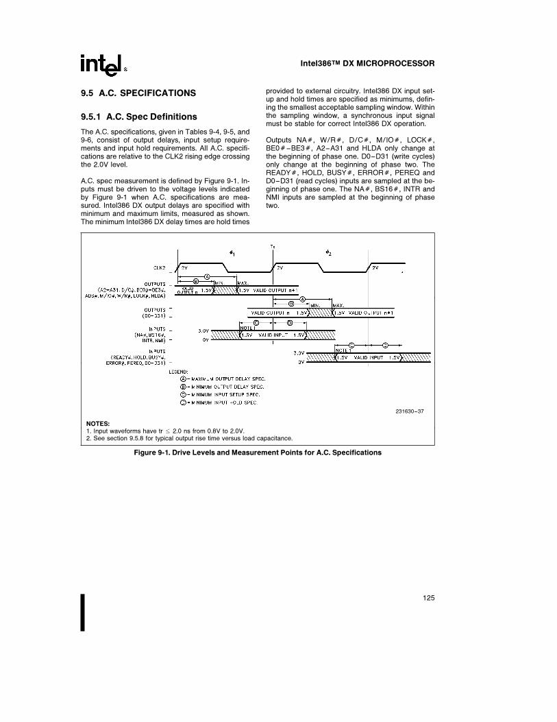
Intel386TM DX MICROPROCESSOR
9.5 A.C. SPECIFICATIONS
9.5.1 A.C. Spec Definitions
The A.C. specifications, given in Tables 9-4, 9-5, and9-6, consist of output delays, input setup require-ments and input hold requirements. All A.C. specifi-cations are relative to the CLK2 rising edge crossingthe 2.0V level.
A.C. spec measurement is defined by Figure 9-1. In-puts must be driven to the voltage levels indicatedby Figure 9-1 when A.C. specifications are mea-sured. Intel386 DX output delays are specified withminimum and maximum limits, measured as shown.The minimum Intel386 DX delay times are hold times
provided to external circuitry. Intel386 DX input set-up and hold times are specified as minimums, defin-ing the smallest acceptable sampling window. Withinthe sampling window, a synchronous input signalmust be stable for correct Intel386 DX operation.
Outputs NAÝ, W/RÝ, D/CÝ, M/IOÝ, LOCKÝ,BE0Ý–BE3Ý, A2–A31 and HLDA only change atthe beginning of phase one. D0–D31 (write cycles)only change at the beginning of phase two. TheREADYÝ, HOLD, BUSYÝ, ERRORÝ, PEREQ andD0–D31 (read cycles) inputs are sampled at the be-ginning of phase one. The NAÝ, BS16Ý, INTR andNMI inputs are sampled at the beginning of phasetwo.
231630–37
NOTES:1. Input waveforms have tr s 2.0 ns from 0.8V to 2.0V.2. See section 9.5.8 for typical output rise time versus load capacitance.
Figure 9-1. Drive Levels and Measurement Points for A.C. Specifications
125
Intel386TM DX MICROPROCESSOR
9.5.2 A.C. Specification TablesFunctional Operating Range: VCC e 5V g5%; TCASE e 0§C to a85§C
Table 9-4. 33 MHz Intel386TM DX A.C. Characteristics
33 MHzRef.
Symbol Parameter Intel386TM DX UnitFig.
Notes
Min Max
Operating Frequency 8 33.3 MHz Half of CLK2 Frequency
t1 CLK2 Period 15.0 62.5 ns 9-3
t2a CLK2 High Time 6.25 ns 9-3 at 2V
t2b CLK2 High Time 4.5 ns 9-3 at 3.7V
t3a CLK2 Low Time 6.25 ns 9-3 at 2V
t3b CLK2 Low Time 4.5 ns 9-3 at 0.8V
t4 CLK2 Fall Time 4 ns 9-3 3.7V to 0.8V (Note 3)
t5 CLK2 Rise Time 4 ns 9-3 0.8V to 3.7V (Note 3)
t6 A2–A31 Valid Delay 4 15 ns 9-5 CL e 50 pF
t7 A2–A31 Float Delay 4 20 ns 9-6 (Note 1)
t8 BE0Ý–BE3Ý, LOCKÝ Valid Delay 4 15 ns 9-5 CL e 50 pF
t9 BE0Ý–BE3Ý, LOCKÝ Float Delay 4 20 ns 9-6 (Note 1)
t10 W/RÝ, M/IOÝ, D/CÝ, Valid Delay 4 15 ns 9-5 CL e 50 pF
t10a ADSÝ Valid Delay 4 14.5 ns 9-5 CL e 50 pF
t11 W/RÝ, M/IOÝ, D/CÝ, ADSÝ Float Delay 4 20 ns 9-6 (Note 1)
t12 D0–D31 Write Data Valid Delay 7 24 ns 9-5a CL e 50 pF, (Note 4)
t12a D0–D31 Write Data Hold Time 2 9-5b CL e 50 pF
t13 D0–D31 Float Delay 4 17 ns 9-6 (Note 1)
t14 HLDA Valid Delay 4 20 ns 9-6 CL e 50 pF
t15 NAÝ Setup Time 5 ns 9-4
t16 NAÝ Hold Time 2 ns 9-4
t17 BS16Ý Setup Time 5 ns 9-4
t18 BS16Ý Hold Time 2 ns 9-4
t19 READYÝ Setup Time 7 ns 9-4
t20 READYÝ Hold Time 4 ns 9-4
126
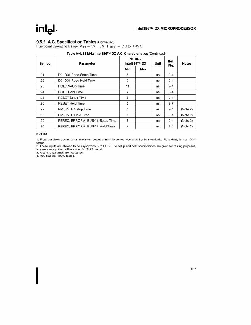
Intel386TM DX MICROPROCESSOR
9.5.2 A.C. Specification Tables (Continued)
Functional Operating Range: VCC e 5V g5%; TCASE e 0§C to a85§C
Table 9-4. 33 MHz Intel386TM DX A.C. Characteristics (Continued)
33 MHzRef.
Symbol Parameter Intel386TM DX UnitFig.
Notes
Min Max
t21 D0–D31 Read Setup Time 5 ns 9-4
t22 D0–D31 Read Hold Time 3 ns 9-4
t23 HOLD Setup Time 11 ns 9-4
t24 HOLD Hold Time 2 ns 9-4
t25 RESET Setup Time 5 ns 9-7
t26 RESET Hold Time 2 ns 9-7
t27 NMI, INTR Setup Time 5 ns 9-4 (Note 2)
t28 NMI, INTR Hold Time 5 ns 9-4 (Note 2)
t29 PEREQ, ERRORÝ, BUSYÝ Setup Time 5 ns 9-4 (Note 2)
t30 PEREQ, ERRORÝ, BUSYÝ Hold Time 4 ns 9-4 (Note 2)
NOTES:
1. Float condition occurs when maximum output current becomes less than ILO in magnitude. Float delay is not 100%tested.2. These inputs are allowed to be asynchronous to CLK2. The setup and hold specifications are given for testing purposes,to assure recognition within a specific CLK2 period.3. Rise and fall times are not tested.4. Min. time not 100% tested.
127

Intel386TM DX MICROPROCESSOR
9.5.2 A.C. Specification Tables (Continued)
Functional Operating Range: VCC e 5V g5%; TCASE e 0§C to a85§C
Table 9-5. 25 MHz Intel386TM DX A.C. Characteristics
25 MHzRef.
Symbol Parameter Intel386TM DX UnitFig.
Notes
Min Max
Operating Frequency 4 25 MHz Half of CLK2 Frequency
t1 CLK2 Period 20 125 ns 9-3
t2a CLK2 High Time 7 ns 9-3 at 2V
t2b CLK2 High Time 4 ns 9-3 at 3.7V
t3a CLK2 Low Time 7 ns 9-3 at 2V
t3b CLK2 Low Time 5 ns 9-3 at 0.8V
t4 CLK2 Fall Time 7 ns 9-3 3.7V to 0.8V
t5 CLK2 Rise Time 7 ns 9-3 0.8V to 3.7V
t6 A2–A31 Valid Delay 4 21 ns 9-5 CL e 50 pF
t7 A2–A31 Float Delay 4 30 ns 9-6 (Note 1)
t8 BE0Ý–BE3Ý Valid Delay 4 24 ns 9-5 CL e 50 pF
t8a LOCKÝ Valid Delay 4 21 ns 9-5 CL e 50 pF
t9 BE0Ý–BE3Ý, LOCKÝ Float Delay 4 30 ns 9-6 (Note 1)
t10 W/RÝ, M/IOÝ, D/CÝ, ADSÝ Valid Delay 4 21 ns 9-5 CL e 50 pF
t11 W/RÝ, M/IOÝ, D/CÝ, ADSÝ Float Delay 4 30 ns 9-6 (Note 1)
t12 D0–D31 Write Data Valid Delay 7 27 ns 9-5a CL e 50 pF
t12a D0–D31 Write Data Hold Time 2 9-5b CL e 50 pF
t13 D0–D31 Float Delay 4 22 ns 9-6 (Note 1)
t14 HLDA Valid Delay 4 22 ns 9-6 CL e 50 pF
t15 NAÝ Setup Time 7 ns 9-4
t16 NAÝ Hold Time 3 ns 9-4
t17 BS16Ý Setup Time 7 ns 9-4
t18 BS16Ý Hold Time 3 ns 9-4
t19 READYÝ Setup Time 9 ns 9-4
t20 READYÝ Hold Time 4 ns 9-4
128

Intel386TM DX MICROPROCESSOR
9.5.2 A.C. Specification Tables (Continued)
Functional Operating Range: VCC e 5V g5%; TCASE e 0§C to a85§C
Table 9-5. 25 MHz Intel386TM DX A.C. Characteristics (Continued)
25 MHzRef.
Symbol Parameter Intel386TM DX UnitFig.
Notes
Min Max
t21 D0–D31 Read Setup Time 7 ns 9-4
t22 D0–D31 Read Hold Time 5 ns 9-4
t23 HOLD Setup Time 15 ns 9-4
t24 HOLD Hold Time 3 ns 9-4
t25 RESET Setup Time 10 ns 9-7
t26 RESET Hold Time 3 ns 9-7
t27 NMI, INTR Setup Time 6 ns 9-4 (Note 2)
t28 NMI, INTR Hold Time 6 ns 9-4 (Note 2)
t29 PEREQ, ERRORÝ, BUSYÝ Setup Time 6 ns 9-4 (Note 2)
t30 PEREQ, ERRORÝ, BUSYÝ Hold Time 5 ns 9-4 (Notes 2, 3)
NOTES:
1. Float condition occurs when maximum output current becomes less than ILO in magnitude. Float delay is not 100%tested.2. These inputs are allowed to be asynchronous to CLK2. The setup and hold specifications are given for testing purposes,to assure recognition within a specific CLK2 period.3. Symbol Parameter Min
TC e 0§C t30 PEREQ, ERRORÝ, BUSYÝ Hold Time 4TC e a85§C t30 PEREQ, ERRORÝ, BUSYÝ Hold Time 5
129
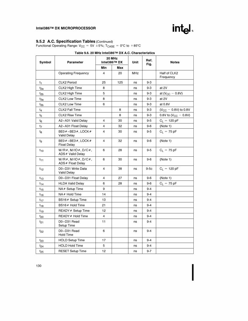
Intel386TM DX MICROPROCESSOR
9.5.2 A.C. Specification Tables (Continued)
Functional Operating Range: VCC e 5V g5%; TCASE e 0§C to a85§C
Table 9.6. 20 MHz Intel386TM DX A.C. Characteristics
20 MHzRef.
Symbol Parameter Intel386TM DX UnitFig.
Notes
Min Max
Operating Frequency 4 20 MHz Half of CLK2Frequency
t1 CLK2 Period 25 125 ns 9-3
t2a CLK2 High Time 8 ns 9-3 at 2V
t2b CLK2 High Time 5 ns 9-3 at (VCC b 0.8V)
t3a CLK2 Low Time 8 ns 9-3 at 2V
t3b CLK2 Low Time 6 ns 9-3 at 0.8V
t4 CLK2 Fall Time 8 ns 9-3 (VCC b 0.8V) to 0.8V
t5 CLK2 Rise Time 8 ns 9-3 0.8V to (VCC b 0.8V)
t6 A2–A31 Valid Delay 4 30 ns 9-5 CL e 120 pF
t7 A2–A31 Float Delay 4 32 ns 9-6 (Note 1)
t8 BE0Ý–BE3Ý, LOCKÝ 4 30 ns 9-5 CL e 75 pFValid Delay
t9 BE0Ý–BE3Ý, LOCKÝ 4 32 ns 9-6 (Note 1)Float Delay
t10 W/RÝ, M/IOÝ, D/CÝ, 6 28 ns 9-5 CL e 75 pFADSÝ Valid Delay
t11 W/RÝ, M/IOÝ, D/CÝ, 6 30 ns 9-6 (Note 1)ADSÝ Float Delay
t12 D0–D31 Write Data 4 38 ns 9-5c CL e 120 pFValid Delay
t13 D0–D31 Float Delay 4 27 ns 9-6 (Note 1)
t14 HLDA Valid Delay 6 28 ns 9-6 CL e 75 pF
t15 NAÝ Setup Time 9 ns 9-4
t16 NAÝ Hold Time 14 ns 9-4
t17 BS16Ý Setup Time 13 ns 9-4
t18 BS16Ý Hold Time 21 ns 9-4
t19 READYÝ Setup Time 12 ns 9-4
t20 READYÝ Hold Time 4 ns 9-4
t21 D0–D31 Read 11 ns 9-4Setup Time
t22 D0–D31 Read 6 ns 9-4Hold Time
t23 HOLD Setup Time 17 ns 9-4
t24 HOLD Hold Time 5 ns 9-4
t25 RESET Setup Time 12 ns 9-7
130
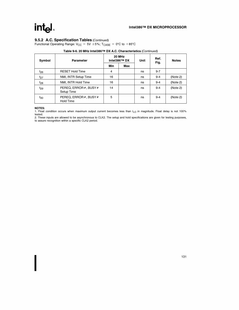
Intel386TM DX MICROPROCESSOR
9.5.2 A.C. Specification Tables (Continued)
Functional Operating Range: VCC e 5V g5%; TCASE e 0§C to a85§C
Table 9-6. 20 MHz Intel386TM DX A.C. Characteristics (Continued)
20 MHzRef.
Symbol Parameter Intel386TM DX UnitFig.
Notes
Min Max
t26 RESET Hold Time 4 ns 9-7
t27 NMI, INTR Setup Time 16 ns 9-4 (Note 2)
t28 NMI, INTR Hold Time 16 ns 9-4 (Note 2)
t29 PEREQ, ERRORÝ, BUSYÝ 14 ns 9-4 (Note 2)
Setup Time
t30 PEREQ, ERRORÝ, BUSYÝ 5 ns 9-4 (Note 2)
Hold Time
NOTES:1. Float condition occurs when maximum output current becomes less than ILO in magnitude. Float delay is not 100%tested.2. These inputs are allowed to be asynchronous to CLK2. The setup and hold specifications are given for testing purposes,to assure recognition within a specific CLK2 period.
131

Intel386TM DX MICROPROCESSOR
9.5.3 A.C. Test Loads
231630–38
CL e 120 pF on A2–A31, D0–D31CL e 75 pF on BE0Ý–BE3Ý, W/RÝ , M/IOÝ , D/CÝ , ADSÝ,LOCKÝ, HLDACL includes all parasitic capacitances.
Figure 9-2. A.C. Test Load
9.5.4 A.C. Timing Waveforms
231630–39
Figure 9-3. CLK2 Timing
231630–40
Figure 9-4. Input Setup and Hold Timing
132
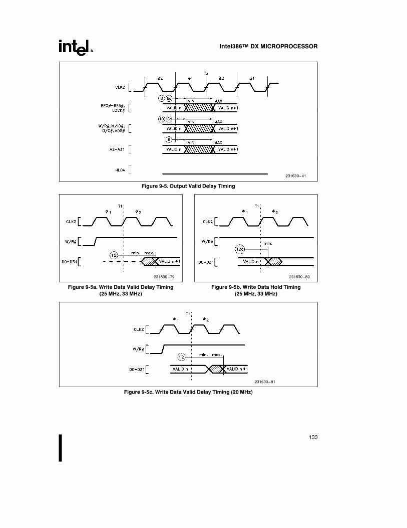
Intel386TM DX MICROPROCESSOR
231630–41
Figure 9-5. Output Valid Delay Timing
231630–79 231630–80
Figure 9-5a. Write Data Valid Delay Timing
(25 MHz, 33 MHz)
Figure 9-5b. Write Data Hold Timing
(25 MHz, 33 MHz)
231630–81
Figure 9-5c. Write Data Valid Delay Timing (20 MHz)
133

Intel386TM DX MICROPROCESSOR
9.5.5 Typical Output Valid Delay Versus Load Capacitanceat Maximum Operating Temperature (CL e 120 pF)
231630–77
NOTE:This graph will not be linear outside of the CL range shown.
9.5.6 Typical Output Valid Delay Versus Load Capacitanceat Maximum Operating Temperature (CL e 75 pF)
231630–82
NOTE:This graph will not be linear outside of the CL range shown.
134
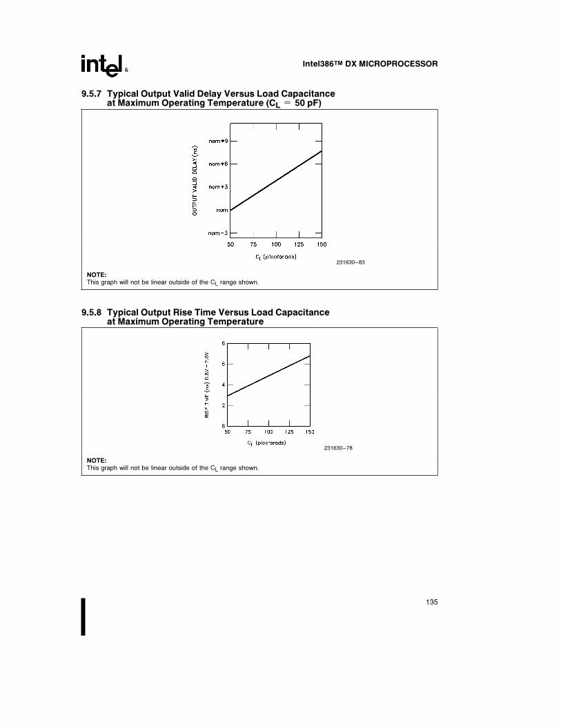
Intel386TM DX MICROPROCESSOR
9.5.7 Typical Output Valid Delay Versus Load Capacitanceat Maximum Operating Temperature (CL e 50 pF)
231630–83
NOTE:This graph will not be linear outside of the CL range shown.
9.5.8 Typical Output Rise Time Versus Load Capacitanceat Maximum Operating Temperature
231630–78
NOTE:This graph will not be linear outside of the CL range shown.
135
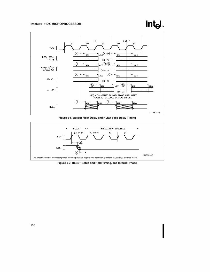
Intel386TM DX MICROPROCESSOR
231630–42
Figure 9-6. Output Float Delay and HLDA Valid Delay Timing
231630–43The second internal processor phase following RESET high-to-low transition (provided t25 and t26 are met) is w2.
Figure 9-7. RESET Setup and Hold Timing, and Internal Phase
136

Intel386TM DX MICROPROCESSOR
10. REVISION HISTORY
This Intel386 DX data sheet, version -005, contains updates and improvements to previous versions. A revi-sion summary is listed here for your convenience.
The sections significantly revised since version -001 are:
2.9.6 Sequence of exception checking table added.
2.9.7 Instruction restart revised.
2.11.2 TLB testing revised.
2.12 Debugging support revised.
3.1 LOCK prefix restricted to certain instructions.
4.4.3.3 I/O privilege level and I/O permission bitmap added.
Figures 4-15a, 4-15b I/O permission bitmap added.
4.6.4 Protection and I/O permission bitmap revised.
4.6.6 Entering and leaving virtual 8086 mode through task switches, trap and interruptgates, and IRET explained.
5.6 Self-test signature stored in EAX.
5.8 Coprocessor interface description added.
5.8.1 Software testing for coprocessor presence added.
Table 6-3 PGA package thermal characteristics added.
7. Designing for ICE-Intel386 revised.
Figures 7-8, 7-9, 7-10 ICE-Intel386 clearance requirements added.
6.2.3.4 Encoding of 32-bit address mode with no ‘‘sib’’ byte corrected.
The sections significantly revised since version -002 are:
Table 2-5 Interrupt vector assignments updated.
Figure 4-15a BitÐmapÐoffset must be less than or equal to DFFFH.
Figure 5-28 Intel386 DX outputs remain in their reset state during self-test.
5.7 Component and revision identifier history updated.
9.4 20 MHz D.C. specifications added.
9.5 16 MHz A.C. specifications updated. 20 MHz A.C. specifications added.
Table 6-1 Clock counts updated.
The sections significantly revised since version -003 are:
Table 2-6b Interrupt priorities 2 and 3 interchanged.
2.9.8 Double page faults do not raise double fault exception.
Figure 4-5 Maximum-sized segments must have segments Base11..0 e 0.
5.4.3.4 BS16Ý timing corrected.
Figures 5-16, 5-17, BS16Ý timing corrected. BS16Ý must not be asserted once NAÝ has been
5-19, 5-22 sampled asserted in the current bus cycle.
9.5 16 MHz and 20 MHz A.C. specifications revised. All timing parameters are nowguaranteed at 1.5V test levels. The timing parameters have been adjusted toremain compatible with previous 0.8V/2.0V specifications.
137

Intel386TM DX MICROPROCESSOR
The sections significantly revised since version -004 are:
Chapter 4 25 MHz Clock data included.
Table 2-4 Segment Register Selection Rules updated.
5.4.4 Interrupt Acknowledge Cycles discussion corrected.
Table 5-10 Additional Stepping Information added.
Table 9-3 ICC values updated.
9.5.2 Table for 25 MHz A.C. Characteristics added. A.C. Characteristics tables reor-dered.
Figure 9-5 Output Valid Delay Timing Figure reconfigured. Partial data now provided in addi-tional Figures 9-5a and 9-5b.
Table 6-1 Clock counts updated and formats corrected.
The sections significantly revised since version -005 are:
Table of Contents Simplified.
Chapter 1 Pin Assignment.
2.3.6 Control Register 0.
Table 2-4 Segment override prefixes possible.
Figure 4-6 Note added.
Figure 4-7 Note added.
5.2.3 Data bus state at end of cycle.
5.2.8.4 Coprocessor error.
5.5.3 Bus activity during and following reset.
Figure 5-28 ERRORÝ.
Chapter 6 Moved forward in datasheet.
Chapter 7 Moved forward in datasheet.
Chapter 8 Upgraded to chapter.
Table 9-3 25 MHz ICC Typ. value corrected.
Table 9-3 33 MHz D.C. Specifications added.
Table 9-4 33 MHz A.C. Specifications added.
Figure 9-5 t8a and t10a added.
Figure 9-5c Added.
9.5.6 Added derating for CL e 75 pF.
9.5.7 Added derating for CL e 50 pF.
Figure 9.6 t8a and t10a added.
The sections significantly revised since version -006 are:
2.3.4 Alignment of maximum sized segments.
2.9.8 Double page faults do not raise double fault exception.
5.5.3 ERRORÝ and BUSYÝ sampling after RESET.
Figure 5-21 BS16Ý timing altered.
Figure 5-26 READYÝ timing altered.
Figure 5-28 ERRORÝ timing corrected.
6.2.3.1 Corrected Encoding of Register Field Chart.
Chapter 7 Updated ICE-Intel386 DX information.
9.5.2 Remove preliminary stamp on 25 MHz A.C. Specifications.
9.5.2 Remove preliminary stamp on 33 MHz A.C. Specifications.
138

Intel386TM DX MICROPROCESSOR
The sections significantly revised since version -007 are:
Table of Contents Page numbers revised.
Figure 5-15 BS16Ý timing altered.
Figure 5-22 Previous cycle, T2 changed to Idle cycle, Ti.
6.1 Note about wait states added.
Table 6-1 Opcodes for AND, OR, and XOR instructions corrected.
Table 6-1 Bits 3, 4, and 5 of the ‘‘mod r/m’’ byte corrected for the LTR instruction.
Table 8-2 Reference to Figure 6-4 should be reference Figure 8-2.
Table 8-2 Note Ý4 added.
The sections significantly revised since version -008 are:
Table 9-3 20, 25, 33 MHz ICC specifications updated.
139